Embed Size (px)
Citation preview
Feature article
54 Renewable Energy Focus July/August 2007
Cost: the big issue
One of the main challenges the
PV industry faces is to make solar
electricity cost eff ective across a
wider range of scenarios.
“One of the biggest hurdles that the
total solar industry has to overcome
is how we can bring down the cost,”
Kyocera general manager Hidehito
Hisa told us. “Right now solar
power is one of most expensive
technologies you can buy. Some day
the power generated by solar has to
be equal or below the conventional
grid energy source.”
In the last three decades,
significant research has been
carried out to reduce the cost,
and the price of solar modules
has gone down from US$21/watt
in 1984 to about US$3/watt in
2006.
Today, if you live away from the main grid, and the choice of obtaining electricity is from
diesel power or PV, solar cells
are already cost-effective.
Many countries already offer
incentives to encourage the use
of PV systems, and the market
has been growing annually at
more than 20%, with a total
revenue exceeding US$10 billion
in 2006 (see FIT for purpose, page
60).
PV: where are we now?RENEWABLE ENERGY FOCUS TAKES A SNAPSHOT OF CURRENT
DEVELOPMENTS IN PV, AND INVESTIGATES TO WHAT EXTENT CRYSTALLINE
TECHNOLOGY WILL CONTINUE TO BE THE MAINSTAY OF THE INDUSTRY. David Hopwood
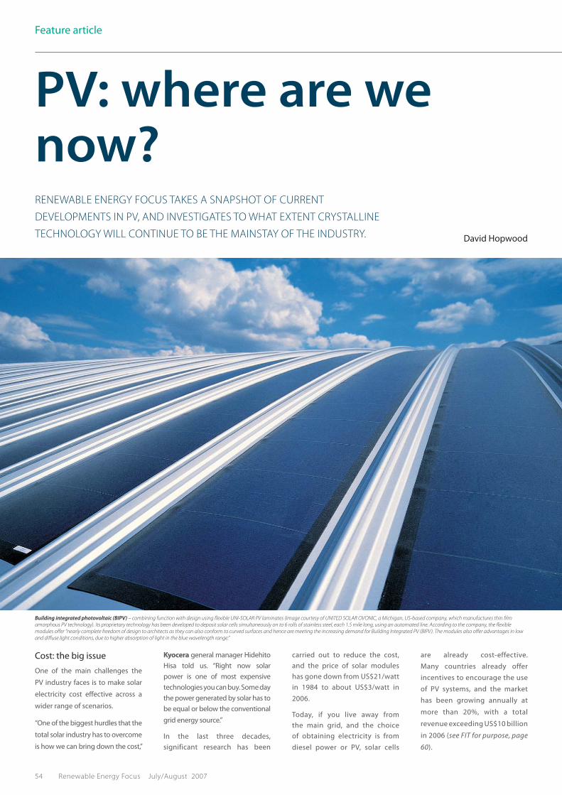
Building integrated photovoltaic (BIPV) – combining function with design using fl exible UNI-SOLAR PV laminates (Image courtesy of UNITED SOLAR OVONIC, a Michigan, US-based company, which manufactures thin fi lm amorphous PV technology). Its proprietary technology has been developed to deposit solar cells simultaneously on to 6 rolls of stainless steel, each 1.5 mile long, using an automated line. According to the company, the fl exible modules off er “nearly complete freedom of design to architects as they can also conform to curved surfaces and hence are meeting the increasing demand for Building Integrated PV (BIPV). The modules also off er advantages in low and diff use light conditions, due to higher absorption of light in the blue wavelength range.”
ref_0804_pg54_59.indd 54ref_0804_pg54_59.indd 54 25/07/2007 15:18:0225/07/2007 15:18:02
Sub_Electricity (PV)/Cat_Solar
Renewable Energy Focus July/August 2007 55
Material challenges – is less more?
The fi rst solar cells used were
crystalline silicon wafers, and the
workhorse of the industry is still
single crystal or polycrystalline
silicon-based solar cells. The
manufacturing process is,
however, energy-intensive, and
there are many steps involved that
make the product expensive. The
modules have glass covers that
are fragile, and need expensive
support structures to install.
There are many ways in which
companies are trying to reduce
the cost of PV technology, such as
reducing the amount of material
per module.
Companies like CSG Solar have
designed technology that allows
the production of solar modules
using less than 2µm thick crystalline
silicon – placed on a textured sheet
of glass. This enables CSG modules
to capture the established strengths
of crystalline silicon, in a much
thinner and cost-eff ective form. “All
other thin fi lm contenders use more
exotic semiconductor materials and
so miss out on the proven durability
and/or environmental benignness
of silicon,” says CSG’s Joanna Ziegler.
“Just about everything in CSG’s
technology is innovative, from the
method of texturing the glass before
the silicon is deposited (enabling
light to eff ectively get trapped in
the thin silicon) to the use of inkjet
printing in the production of the
electrical contacts enabling power
to be extracted from the silicon.”
Thin Film (TFT)
Go to any PV conference though, and
the talk is of thin fi lm technology;
many companies are working on
diff erent thin fi lm technologies,
namely amorphous silicon, copper-
indium-di-selenide and cadmium-
telluride, because they can reduce
the cost of modules substantially.
But compared to crystalline solar
cells the challenge for thin fi lm
technologies lies in increasing the
effi ciency level achieved under
laboratory conditions to mass
production settings. While overall
system costs are already lower using
thin fi lm technologies, increasing
the effi ciency will reduce the larger
area currently required to generate
the same output as crystalline
modules, and assist in reducing the
costs for solar energy.
Whether, and to what extent, thin
fi lm and other novel technologies
will replace crystalline technology is
the subject of intense debate in the
industry. This has been highlighted
by the well-documented silicon
supply problems of the past few
years. According to Professor Eicke
Weber, director of the Fraunhofer
Institute for Solar Energy Systems
ISE in Germany, about 90% of the
market demand is for crystalline
silicon solar cells – with effi ciencies
ranging from 14% to 20% – and
this has created supply problems as
the PV industry competes with the
semiconductor industry for silicon
feedstocks: “there has not been
enough high-purity silicon available
to fulfi l capacities of the production
lines which have been built,” he
says, “and some production lines
are working at only 60% capacity
because of shortages.”
This shortage of material has been a
factor in the price of the PV modules
not coming down as the industry
would have hoped, and this has
been a further catalyst for the
development of newer technologies
such as thin fi lm that allow modules
to be produced at lower cost (it is
easier to deposit these materials on
large areas). “Most of the materials
– even Amorphous silicon – are very
independent from the supply of the
normal high purity silicon from the
crystalline silicon market, so they
are less expensive and they have
more access to the market,” Weber
explains.
But the downside is that these
technologies lack effi ciencies; “for
amorphous silicon you cannot
really buy anything above 8% of
long term stable effi ciency, and
other thin fi lm technologies have a
magic limit near 10%-11%”, he says,
well below what has been achieved
for crystalline technology.
And Weber, who admits that
Fraunhofer doesn’t concentrate
on developing thin fi lm
technologies, believes we need
to be cautious and realistic about
claims that the effi ciency of thin
fi lm will increase dramatically:
“I always read business plans
which predict optimistic jumps
in effi ciency. But just look at the
situation with amorphous silicon
– this is a material which has
been developed in the last 20
years with enormous amounts
of government support; more
government support has been
given to thin fi lm and amorphous
materials than for crystalline
silicon research, but this 20 years’
of research has not done anything
to substantially increase the
effi ciency – increasing effi ciency is
simply constrained by the physics
and the properties of thin solar
cells.”
Market niches for diff erent applications
Of course, he says, that’s not to
say that the thin fi lm technologies
don’t have their place in the
market, or even an important role
to play in keeping a lid on the price
of crystalline silicon PV systems. It’s
all to do with the diff erent needs of
the end user; a trade off between
whether high price/higher
effi ciency is your main concern or
lower price/lower effi ciency will do
the job:
“Right now thin fi lm solar cells
cost around �1-�2/watt, whereas
crystalline silicon solar cells cost
something like �3.50/watt. If you
are in the Sahara desert making a
power plant, for example, you don’t
care too much about the effi ciency
because you have enough area and
you can use the least US$/watt. On
the other hand if you have a house
and a roof, and you live in Northern
Europe, then you have a choice
whether you want to have 1.5Kw or
3Kw PV on your roof. Especially in
places like Germany with its Feed-in
Tariff – where you get paid per Kw/
hour per produced PV power – it
makes sense to pay for the higher
effi ciency.”
Do those involved in the production
of thin fi lm agree with this?
At this year’s Intersolar show, Schott
introduced a new framed version of
its ASI F-90 thin-fi lm module, with
an effi ciency of around 6% [10% at
an R&D scale] which the company
says produces nearly three times as
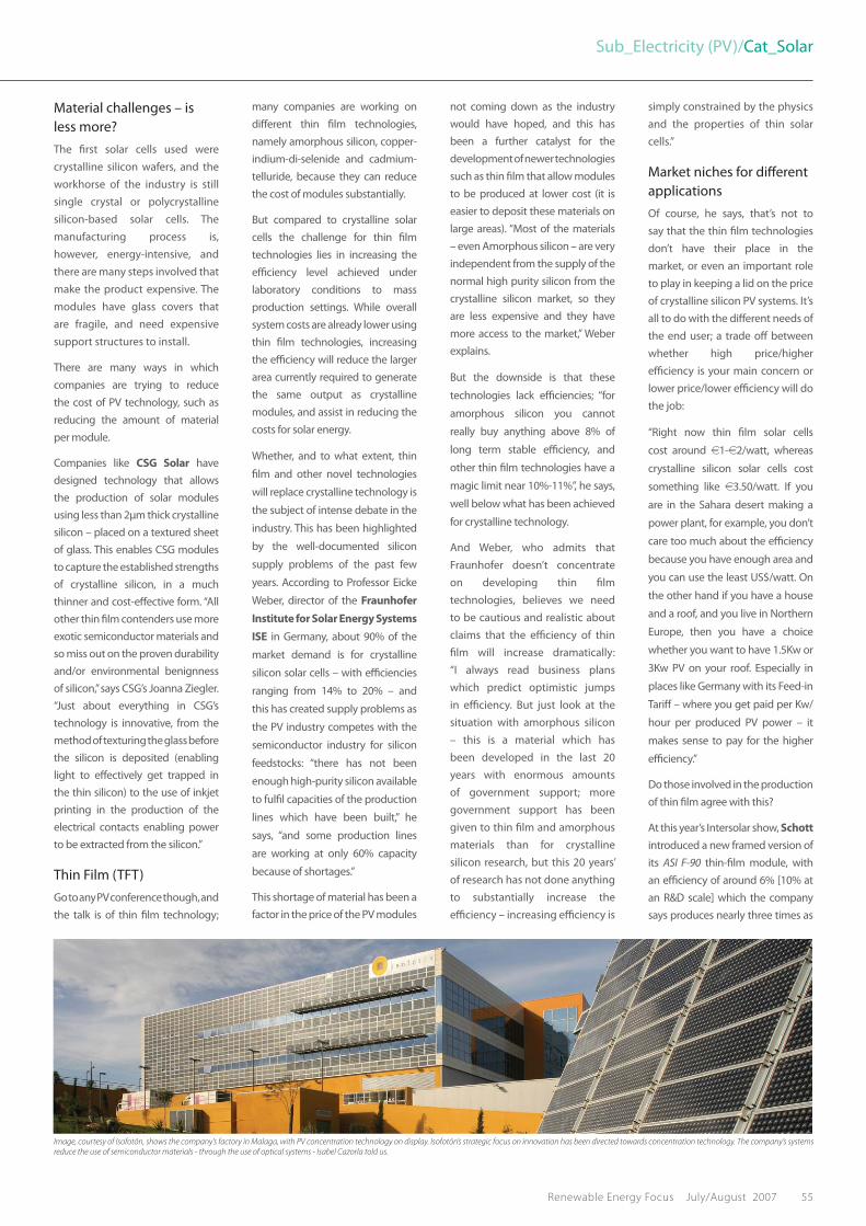
Image, courtesy of Isofotón, shows the company’s factory in Malaga, with PV concentration technology on display. Isofotón’s strategic focus on innovation has been directed towards concentration technology. The company’s systems reduce the use of semiconductor materials - through the use of optical systems - Isabel Cazorla told us.
ref_0804_pg54_59.indd 55ref_0804_pg54_59.indd 55 25/07/2007 15:18:1425/07/2007 15:18:14
Sub_Electricity (PV)/Cat_Solar
56 Renewable Energy Focus July/August 2007
much output as earlier models. The
company points to the use of thin
fi lm where, for example, roofs do
not face exactly the right direction
or off er the perfect angle, or when
temperatures rise signifi cantly
(independent studies reportedly
show that ASI modules can deliver
as much as 10% more power per
watt than crystalline modules),
claims Schott.
Lars Waldmann of Schott adds,
“thin fi lm does have applications
in areas like Building Integrated
PV, because the modules can be
integrated into the building quite
easily, and is more cost effi cient
in terms of price per m2 (and per
watt/peak in the future). Other
applications would be where you
need to keep the costs down in
rural electrifi cation, or in places
where solar radiation is good;
where you might have large
heat loads and the crystalline
PV is going down; and maybe
where you have diff used light
in the jungle or in Asian regions
– in these areas thin fi lm is a good
approach.”
Waldmann also points to larger-
scale ground mounted PV systems
as another application where thin
fi lm would fi t the bill.
Sharp Corp says that it has
successfully developed mass-
production technology for
stacked triple-junction thin-
film solar cells by turning a
conventional two-active-layer
structure (amorphous silicon
plus microcrystalline silicon) into
a triple-junction structure with
amorphous silicon (two active
layers) and microcrystalline
silicon (single active layer).
“This new architecture boosts
cell conversion efficiency
from 11%-13% and module
conversion efficiency from 8.6%-
10%. Creating two amorphous
silicon active layers significantly
increases voltage levels, and
structuring the cell to have three
active layers in combination with
microcrystalline silicon decreases
light-induced degradation (drop
in conversion efficiency)” a
source said.
On how much opportunity there
will be for thin film in coming
years, Weber of Fraunhofer
ISE adds, “I think there will
be enough space for the thin
film manufacturers and the
crystalline silicon manufacturers,
but my expectation is that the
market share of thin film will
never come above 10%-20%. It
will always stay a small segment,
and the biggest growth in the PV
market will be crystalline silicon.
In the next five years, I will be
very happy if thin film PV keeps
the lid on the price of silicon PV
– when the price differential to
silicon modules gets bigger it
will exert very healthy pressure
on the price of silicon modules.”
Waldmann agrees that there is no
way one technology will “replace”
the other. “For the retrofit market
– rooftop mounted PV – this is a
completely different market, and
you find the technology that
works for a certain situation, and
that’s why Schott is engaged in
both of these businesses.”
Purifi ed metallurgical silicon
Both Schott and Fraunhofer point to
other areas of development for PV,
away from the headline-grabbing
thin fi lm technologies.
Fraunhofer continues to push
the effi ciency of high effi ciency
crystalline silicon solar cells (“because
it still makes a diff erence if you can
get 20%, 22% or 24% effi ciency with
reasonably low cost production”).
Additionally, Weber has brought
research that he pioneered at the
University of California, Berkely,
into the Institute. Namely, what
he describes as “PV with unlimited
silicon resources,” or “crystalline
silicon PV based not on the high
purity silicon that the semiconductor
industry is using, but based on dirty
silicon, or purifi ed metallurgical
silicon.
He explains that what is actually in
short supply is the semiconductor
grade silicon, because of the market
shared between the IT and PV
industry.
Using intelligent defect engineering,
it is possible to produce solar cells of
essentially the same (or marginally
lower effi ciency), out of a material
that is practically in unlimited
supply. It also has other advantages;
low cost of production, and it needs
much less energy for production,
something that is important for an
industry that has thus far survived
on the back of its green credentials.
“Of course there is still the energy
required for making modules and
contacts etc, but the silicon part of
the total energy equation can be
substantially decreased by using
the purifi ed metallurgical silicon
concept,” Weber says.
Many would argue that we don’t
need this purifi ed metallurgical
silicon because the production
of semiconductor grade silicon
is currently being ramped up.
Weber’s response is that “if the
semiconductor grade silicon
comes down from the current price
(US$100-US$200/kg) to US$50/
kg (maybe a long-term price for
semiconductor silicon) and the
purifi ed metallurgical silicon can be
made for US$10-US$20 per kg there
is still a substantial diff erence.”
Organics
As part of Schott’s strategy, the
company is one of the few companies
looking into organic PV – together
with large companies like Bosch
and BASF. Organic PV is the term
used to describe solar cells based on
organic semi-conductive materials
that can generate electricity from
light. This means that, in the future,
they could replace the silicon that is
used today. The aim is to use new
materials, production processes and
installation technologies to make
the organic solar cells more effi cient
and cost-eff ective in the long term.
Furthermore, the new technology
will pave the way for sustainable
energy production and make solar
power more competitive.
ref_0804_pg54_59.indd 56ref_0804_pg54_59.indd 56 25/07/2007 15:18:2025/07/2007 15:18:20
Sub_Electricity (PV)/Cat_Solar
58 Renewable Energy Focus July/August 2007
Organic solar cells are fl exible and
as thin as a clear plastic folder.
They are both light and colour
tunable, which enables them, for
example, to be used in foldable
cell phone chargers, or on car
roofs.
From 2015 onwards, their main area
of application is expected to be in
the construction industry, where
the cells will be used in the form
of a thin layer of plastic on roofs,
windows or facades.
Tracking devices
Another important exploratory
focus lies in light concentrator
technology. Sharp Solar for
example, has developed a solution
that is not based on silicon. The
light is gathered by a fresnel-lense
and concentrated 700 times upon
a III-V compound solar-cell. The cell
itself is very small and reaches an
effi ciency of more than 37% under
concentration. A light-gathering
system already in operation
consists of 270 cells and a two-
axis tracking device. So especially
for the regions where large DNI
is available, the concentrator
represents an interesting
alternative to crystalline modules,
the company reports.
And Conergy’s Thorsten
Vespermann says that Conergy
has developed the SolarOptimus
tracking system, where, in sunny
regions, tracking systems can
“increase electricity output by up
to 35%.”
PV R&D roundup
Although the PV solar market
is dominated by mono/
multicrystalline silicon,
alternatives such as dye-
sensitised; polymer and
thin-fi lm amorphous; CdTe;
CIGS; CIS; and GaAs have not
abandoned the fi ght. Fuji
Keizai USA Inc predicts an
annual average growth of
43.1% for new technologies
over the next decade – to 13%
of the Mw market capacity;
Two newcomers on the block
are California’s Stion (US$15m
in series B funding) and UK’s
Imperial College, London
spin-off Quantasol (US$2.7m
seed funding). Formerly
NStructures, Stion uses TFT; it
is not using Si or CdTe, and is
thought to be taking a quantum
dot approach. Quantasol is
take a GaAs quantum well with
a tandem cell approach (fewer
junctions than the traditional
■
■
triple-junction cell) and
optimised spectral output for
its concentrator system;
Another newcomer is US
R&D fi rm Illuminex, which
has attracted more than
US$2m funding for nanowire
applications, among them PV
thread from Si nanowires and
conducting polymers;
In the US Prime Solar received
DOE funds of US$3m for 18
months work, to scale up
NREL’s record 16.5% CdTe cells
to “dramatically lower the
cost of PV energy generation.”
Simultaneously First Solar
scored fi ve agreements
for the manufacture and
supply of its CdTe modules,
totalling 485Mw sales of some
US$1.28bn. Agreements
include EDF Energies Nouvelles,
Sechilienne-Sidec, the Juwi
Group, SunEdison, and RIO
Energie GmbH. First Solar has
also approved an investment of
US$150m in the construction of
additional manufacturing plants
in Malaysia, rated for 120Mw
and scheduled to be on-line in
late 2009;
On the CIGS front, Arizona-
based Global Solar Energy
won MIL STD-810E ruggedised
■
■
■
certifi cation, claiming no other
fl exible solar product has yet
obtained this. Colorado-based
Ascent Solar, using TF CIGS on
plastic substrate, raised US$20m
from warrant conversions, and is
testing its R2R rapid prototyping
tools prior to operating its
1.5Mw pilot plant by year end,
and starting construction of the
fi rst of four 25Mw large volume
lines;
Solo Power, raising US$30m,
also uses CIGS with an
electrochemical process it
claims is more cost eff ective
than CIGS and Si, being built
on fl exible foil substrates;
Nano Solar with CIGS QDs
and nanoparticle ink and fast
roll printing has production
scheduled by year-end.
Plants in San Jose, California
and Berlin, Germany give it
647,000ft2 for cell and panel
manufacture, as well as R&D;
GaAs fares well, with Emcore’s
PV division awarded US$2m by
NASA’s Jet Propulsion Lab for
the Mars Cruise Stage spacecraft
solar panels, for delivery mid
2008; Aixtron AG has received
an order from Taiwanese WIN
Semiconductors for an ajAIX
2600G3 IC epitaxy reactor to
■
■
■
The magic numbers
What order of effi ciencies might be possible for PV technologies?
Sharp’s new thin fi lm cells consist of three cell layers: two amorphous and
one microcrystalline silicon layer, which convert greater portions of the light
spectrum and further boost effi ciency in comparison with microamorphous
tandem cells (with the cell thickness of just two microns being the same). “The
previous module effi ciency of 8.6% for tandem cells has now been increased
to up to 10% for triple cells”, reports a company source;
Lars Waldmann of Schott says that some companies have achieved
laboratory efficiencies of 21% for Monocrystalline technology [NB: Schott
itself doesn’t manufacture monocrystalline]. And he adds, “for polycrystalline
technology, we stand at 15%-17% on average – in the next five years we
will approach 16%-19%. I see a physical borderline at about 25%, and once
the industry has achieved this I think 36% may be possible, but only in
a 15-20 year R&D timescale. For thin film – cadmium telluride efficiency
is already at 10%. 13% could be achievable, but we don’t see that there
would be any possibility to increase efficiency any further. The next step in
thin film amorphous silicon we predict will be 10%-13%, and this will be a
combination of amorphous silicon, microcrystalline and a special dopine;
At the laboratory level, Kyocera recently reported that it had achieved
the world record in cell effi ciency, 18.5% (measured by Kyocera), with
150mmx155mm multicrystalline silicon.
■
■
■
ref_0804_pg54_59.indd 58ref_0804_pg54_59.indd 58 25/07/2007 15:18:3425/07/2007 15:18:34
Sub_Electricity (PV)/Cat_Solar
Renewable Energy Focus July/August 2007 59
allow WIN to diversify into
solar cell manufacture of triple
junction solar cells;
Solar Millenium AG
(specialising in parabolic
troughs and solar ‘chimneys’)
has begun phase two of its
project near Granada – a solar
thermal facility covering 195ha;
A new test facility at Almeria
in Southern Spain worked by
Fraunhofer Institute for Solar
Energy System is to develop the
100 metre linear Fresnel refl ector
(low cost alternative to parabolic
mirrors) to focus sunlight onto
steel absorber tubes, in which
water is heated to 450oc driving
electricity producing turbines.
This not only improves on
parabolic trough weaknesses,
but is predicted as the route
to provide about 10% of world
electricity by 2050;
Not to be left out of new
developments, PV Powered
has produced a new,
commercial inverter PP30kw
that achieves a 94% CEC
effi ciency rating. The inverter
off ers remote performance
monitoring, night time
disconnect for reduced tare
losses, and a soft start circuit.
Using plastics for solar energy
has increased effi ciency by
6.5% thanks to a discovery at
the Center for Polymers and
Organic Solids (University
of California, Santa Barbara).
Nobel Laureate Alan Heeger
– professor of physics at UC
Santa Barbara, working with
Kwanghee Lee of Korea – has
created a new ‘tandem’ organic
solar cell of two multi-layered
parts working together to
gather a wider range of the
solar radiation spectrum at both
shorter and longer wavelengths.
Heeger is confi dent “we can
make improvements that will
yield effi ciencies suffi ciently
high for commercial products,”
and expects the technology
to be on the market in about
three years. Key element is TiOx,
transparent titanium oxide
which binds and separates the
cells, transporting electrons,
being a collecting layer for the
fi rst cell. As a stable foundation
■
■
■
■
it allows the fabrication of the
second cell to complete the
tandem architecture;
Conergy is investing around
�250 million in what it says is
the world’s fi rst and only fully-
integrated mass production of
wafers, cells and modules. The
fi rst modules, with total output
exceeding 50 megawatt, will
start rolling off the production
lines by the second half of 2007.
By 2008, a production capacity
of 300 Mw for wafers, 275 Mw
for cells and 250 Mw for solar
■
modules will have been reached.
The production process will
begin with a cell thickness of
200 µm but is designed for a
reduction to 160 µm;
Applied Materials focuses the
majority of its eff orts in crystalline
and thin fi lm silicon, although
it is conducting investigations
in other technologies. David
Miller explains, “in crystalline, we
see opportunities for improved
effi ciency driven by the
performance of process tools.
We expect a similar result in thin
■
fi lm silicon because our tools
will provide output that is more
uniform and consistent. This
combined benefi t will produce
more, higher value modules.
This will be true for both the
high throughput (3,300-5,500
uph) crystalline deposition
machine and on the large area
TF production line.”
Thanks to Andrea Bodenhagen
of United Solar Ovonic, and Gail
Purvis who both provided editorial
contributions for this article.
ref_0804_pg54_59.indd 59ref_0804_pg54_59.indd 59 25/07/2007 15:18:4125/07/2007 15:18:41