Embed Size (px)
Citation preview

PWM Control Techniques for Single-Phase
Multilevel Inverter Based Controlled DC Cells
Mahmoud A. Sayed1, Mahrous Ahmed
2,3, Maha G. Elsheikh
2 and Mohamed Orabi
2
1 Electrical Engineering Dept., Faculty of Engineering, South Valley University, Qena, EGYPT.
2 APEARC, Faculty of Engineering, Aswan University, Aswan, EGYPT.
3 Electrical Engineering Department, Faculty of Engineering, Taif University, Taif, KSA.
Abstract
This paper presents a single-phase five-level inverter controlled by two novel Pulse Width Modulation (PWM) switching
techniques. The proposed PWM techniques have been designed based on minimum switching power loss and minimum Total
Harmonic Distortion (THD). In a single-phase five-level inverter employing six switches, the first PWM proposed technique
requires four switches operate at switching frequency and the other two switches at line frequency, whereas the second PWM
proposed technique requires only two switches operate at switching frequency and the others operate at line frequency. Compared
with conventional PWM techniques for single-phase five-level inverter, both of the proposed PWM techniques have the merits of
high efficiency and low harmonic components in the output voltage. The validity of the proposed PWM switching techniques for
controlling the single-phase five-level inverter to regulate load voltage have been verified experimentally using laboratory
prototype based 100V, 500W controlled by dspace-1103.
Key words: Multilevel inverter, single-phase inverter, PWM, voltage control.
I. INTRODUCTION
Recently, the applications of power electronics inverters are
becoming increasingly important. PWM inverters have the
ability to control their output voltage and frequency,
simultaneously. Therefore PWM inverters are considered
power candidate in the industrial applications such as
renewable energy sources, electrical machine drives,
uninterruptible power supplies, and power conversion
applications. Since high efficiency and low harmonic contents
are becoming increasingly important, they introduce new
requirements for the PWM inverters switching techniques and
circuit topologies. The most important issues raised in these
studies are the output voltage levels and the limitation of
switching devices [1], [2].
Multilevel inverters are increasingly being considered for
power electronics applications due to their ability to operate
higher output voltage while producing lower levels of
harmonic components in the switched output voltage since it
has a greater availability of voltage levels [3]–[9]. Also, the
output voltages can be filtered using smaller reactive
components. Moreover, the switching frequencies of the
devices can be reduced and more sinusoidal shaped output
voltage waves can be obtained [10], [11]. Multilevel inverters
is now preferred in high power medium voltage applications
due to the reduced voltage stresses on the devices. Neutral
Point Clamped (NPC) [12], [13], Flying capacitors [14]–[16],
and cascaded H-bridge inverters [17]–[19] are considered the
most famous topologies of the multilevel inverters. However,
the most particular disadvantages of these multilevel inverter
topologies are the large number of the required power
semiconductor switches resulting in high switching power loss.
Although low voltage rate switches can be utilized in a
multilevel inverter, each switch requires a gate drive circuit.
This may cause the overall system to be more expensive and
complex. So, in practical implementation, reducing the number
of switches and hence gate driver circuits have become an
essential research topic [20].
Recently, many topologies of the single-phase multilevel
inverter and its PWM switching techniques have been
published. In [20], combinations of series and parallel switches
have been used to implement the multilevel inverter. However,
this topology uses large number of power switches. In [21], the
multilevel inverter is implemented by using two switches and
two power diodes with the H-bridge single phase inverter.
Those two systems can generate only five levels in the output
voltage. In [22], the conventional single-phase inverter is
converted to a single-phase five level inverter by adding one
switch and four power diodes to the conventional H-bridge
single phase inverter. In [23], a modular inverter that can
produce any required voltage levels has been presented. In
[24], single-phase five-level inverter has been proposed using
only six power switches in addition two coupled inductors and
only one dc supply. However, the size of the coupled inductors
is large. In [25], the idea of single-phase five-level inverter has
been presented using only six power switches in addition to
two floating dc power supplies. However, its control scheme
has been designed based on lookup table. In [26], the idea of a
new topology of a single-phase five-level inverter has been

presented based on minimum number of power switches. It
adopts full-bridge configuration by employing single pulse
control technique based switching angles calculation method.
The harmonic components of the output voltage are determined
by the load inductance in addition to the filter. Therefore, their
harmonic reduction is limited to a certain degree. Furthermore,
the technique of switching angles calculation method requires
off-line calculations of the switching angles and a lookup table.
The same technique has been modified in [27] by using
bidirectional switches, which increases the number of power
switches used in the cascaded controlled dc cells. In [28], the
same technique has been used to obtain a single-phase
multilevel inverter using conventional power switches.
However, each dc supply has been controlled by two switches.
To overcome these limitations, in [29], the authors have
proposed a new PWM switching technique for controlling the
single-phase five-level inverter based on high efficiency and
low harmonics.
Motivated by the aforementioned issues, this paper presents
two novel control PWM switching techniques for controlling a
stand-alone single-phase five-level inverter. The structure of
the inverter uses two power switches controlling the dc input
voltage of a conventional H-bridge inverter. In both control
schemes, some switches operate at high switching frequency
and the others operate at fundamental line frequency in order to
reduce the switching power loss. Proportional-Integral (PI)
controller is used to achieve load voltage to be same as the
reference one. Theoretical analysis, numerical simulation and
laboratory prototype with several experimental results are
presented in order to investigate the capability of the proposed
PWM switching schemes in controlling the load voltage in
addition to confirm the characteristics of the proposed inverter.
II. CONFIGURATION AND OPERATIONAL
PRINCIPLE OF THE PROPOSED INVERTER
The proposed structure of the single-phase multilevel
inverter is shown in Fig. 1. It consists of n-cells connected in
series, one cell is a dc supply whereas the other cells have dc
supply controlled by two switches ( , ), where (
). The switch ( ) is connected in series with the dc
voltage source and the other switch ( ) is connected in
parallel with both the dc voltage source and the series switch
( ). According to the proposed configuration shown in Fig.
1, each cell controlled by two switches has two output voltage
states; zero voltage and the dc voltage source associated with
the considered cell. Since cell-n has only dc voltage source, it
has only one state voltage which is the value of its dc supply.
Therefore, the dc bus voltage has (n) states based on the
values of ( ), as shown in Fig. 2. It is cleared that
the dc bus shown in Fig. 1 has no zero state voltage.
Therefore, cell-n is the basic cell that must be included at any
multilevel inverter based on the proposed topology.
Fig. 1. Configuration of single-phase multilevel inverter.
Fig. 2. Voltage levels of the dc bus.
Conventional H-bridge inverter is connected at the dc bus
terminals to convert the dc voltage to switched bipolar voltage
limited by the value of dc voltage at the dc bus. The H-bridge
inverter consists of four switches ( ), as
shown in Fig.1. The main function of the H-bridge inverter is
to obtain the zero state voltage on the ac load by considering
the switches and or and to be on, simultaneously,
in addition to obtaining the positive half-cycle by considering
the switches and to be on and the negative half-cycle by
considering the switches and to be on. Obviously, this
structure can reduce the number of switches compared to the
conventional topologies used in single-phase multilevel
inverter without affecting the inverter performances, since the
zero state voltage can be generated using either the upper or
lower switches of the H-bridge inverter.
III. PROPOSED SINGLE-PHASE FIVE-LEVEL
INVERTER
In order to generate five levels of the proposed inverter
shown in Fig. 1, the number of the required cascaded cell is
two; (n = 2). One cell has a dc supply controlled by two
switches and the other cell has only a dc supply.
Load
Q1
Q4
Q3
Q2
S11
S12
S22
S21
S(n-1)1
S(n-1)2
V1
V2
V(n-1)
Vn
Cell-1
Cell-2
a b
DC BusVab
Cell-(n-1)
Cell-n
V1
V1+V2
V1+V2+V3
V1+V2+..+V(n-1)+Vn
V1+V2+..+V(n-1)
Vdc
0 V
0 T/2 T

Fig. 3. Model of single-phase five-level inverter.
TABLE I
SWITCHING STATES OF THE SINGLE-PHASE FIVE-LEVEL INVERTER
States ON switches
a
b
c
d
e
f
g
h
i
j
, and
, and
, and
, and
and or and
and or and
, and
, and
, and
, and
Fig. 3 shows the configuration of the proposed single-phase
five-level inverter. Two switches are added to the
conventional single-phase H-bridge inverter in order to
perform a single- phase five-level inverter. In order to achieve
a balanced output voltage levels, the dc voltage sources in
both cells are typical; . The dc bus voltage
will have two states; ( ). The load output voltage
will have five states; ( ).
The load voltage zero state can be generated either by
switching simultaneously the upper switches or the lower
switches of the H-bridge inverter. The other four states can be
generated from the DC Bus voltage .
Since the load current is bi-directional regardless of the load
voltage, operation of the proposed single-phase five- level
inverter has 10 switching states, as illustrated in Fig. 4 and
Table I. The switching patterns of the proposed inverter are
shown in Fig. 4, whereas the load current directions at each
load voltage level state according to switch ON-OFF
conditions are shown in Table I. The conventional
freewheeling states (zero voltage states) are shown in Fig. 4
(e) and (f). The other output voltage levels even + or − can be
achieved by switching the conventional H-bridge inverter with
the control of cell-1 switches ( and ). PWM switching
technique is required to control the single-phase five-level
inverter to achieve the reference load voltage based on the 10
switching patterns shown in Fig. 4 and Table I.
IV. SWITCHING ALGORITHMS FOR THE PROPOSED
PWM SWITCHING TECHNIQUES
Switching frequency and ON-OFF terminal voltage of
power semiconductor devices are the main factors affecting
the inverter power loss and harmonic contents. Motivated
by that, two PWM switching techniques are proposed to
control the single-phase five-level inverter. Switching loss
and harmonic distortion have been considered in both
techniques by operating some switches at high frequency
and the others at fundamental line frequency.
A. Technique-I
The first proposed PWM switching technique for the
single- phase five-level inverter is basically depending on
generating gate signals by comparing rectified reference
waveform with two in-phase triangle carriers having same
frequency, same peak-to-peak, but different offset voltages.
Fig. 5 shows the switching patterns of the single-phase five-
level inverter using PWM Technique-I. The intersection
points between carrier A and carrier B with the reference
waveform decide the inverter output voltage level. The first
level of the inverter output voltage is generated at the
intersection points of the reference voltage waveform and the
lower carrier signal (carrier A), whereas the second level of
the output voltage is generated at the intersection
points of the reference voltage waveform and the upper
carrier signal (carrier B). The positive half-cycle of the
reference voltage waveform is responsible for generating the
positive dc voltage levels ( and ) in the output
voltage, whereas the rectified half-cycle is responsible for
generating the negative dc voltage levels ( and ).
According to the reference voltage, the intersection with the
carrier may happen with the lower carrier only resulting in
modulation index between zero and 0.5, or with both carrier
signals resulting in modulation index between 0.5 and 1.
Therefore, if the modulation index is less than or equals 0.5,
the output voltage of the inverter will have only three levels
( , , and ). On the other hand, if the modulation
index is more than 0.5, the output voltage of the inverter will
have five levels ( , , , , and ). According
to the amplitude of the reference voltage, its period can be
divided into five intervals based on four modes (Mode A,
Mode B, Mode C, and Mode D). Based on the related
displacement phase angles ( ), shown in Fig.
5, the operational modes can be defined as follows:
(1)
The modulation index ( ) of the proposed single-phase
five-level inverter is defined as follows:
Load
Q1
Q4
Q3
Q2
S11
S12
V1
V2
a bDC Bus
Vab
Cell-1
Cell-2
(2)
where is the peak value of the reference modulating
waveform, and is the peak-to-peak value of the carrier.
Also, the frequency ratio ( ) is defined as follows:
(3)
where is the frequency of the carrier signals, and is the
frequency of the modulating signal.
Fig. 5 shows that the displacement phase angles
( ) are affected by the modulation index
( ), If the modulation index is less than or equal 0.5, the
displacement phase angles will be defined as follows:
(4)
If the modulation index is greater than 0.5, the
displacement phase angles will be defined as follows:
(
)
(5)
According to the intersections between the modulation
waveform and the carrier signals, the period of the
reference voltage ( ) is divided into six time intervals
defined as ( ), as shown in Fig. 5.
The signals and , shown in Fig. 5 result from
comparing the modulation waveform with the lower and
upper triangle carriers, respectively. The gate signals of the
proposed inverter switches can be calculated based on the
resultant signals and in addition to the six time
intervals ( ). The resultant gate signals
of the inverter six switches can be formulated as follows:
(( ) ) (( ) )
(( ) ) (( ) )
((( ) ( )) ) (( ) )
( )
(6)
It is cleared from (6) and Fig. 5 that the inverter power
switches ( ) are complementary switches operating
at the fundamental line frequency (i.e. 50 Hz). Also, the
power switches ( ) cannot switching ON
simultaneously. However, their switching signals are decided
based on (6) and operating at switching frequency. Moreover,
the power switches ( ) are complementary switches
operating at switching frequency.
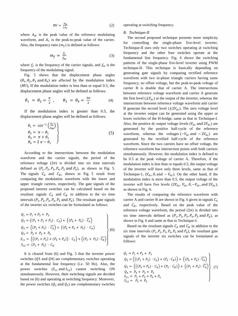
B. Technique-II
The second proposed technique presents more simplicity
for controlling the single-phase five-level inverter.
Technique-II uses only two switches operating at switching
frequency and the other four switches operate at the
fundamental line frequency. Fig. 6 shows the switching
patterns of the single-phase five-level inverter using PWM
technique-II. This technique is basically depending on
generating gate signals by comparing rectified reference
waveform with two in-phase triangle carriers having same
frequency, no offset voltage, but the peak-to-peak voltage of
carrier B is double that of carrier A. The intersections
between reference voltage waveform and carrier A generate
the first level ( ) at the output of the inverter, whereas the
intersections between reference voltage waveform and carrier
B generate the second level ( ). The zero voltage level
at the inverter output can be generated using the upper or
lower switches of the H-bridge, same as that in Technique-I.
Also, the positive dc output voltage levels ( ) are
generated by the positive half-cycle of the reference
waveform, whereas the voltages ( ) are
generated by the rectified half-cycle of the reference
waveform. Since the two carriers have no offset voltage, the
reference waveform has intersection points with both carriers
simultaneously. However, the modulation index is defined to
be 0.5 at the peak voltage of carrier A. Therefore, if the
modulation index is less than or equals 0.5, the output voltage
of the inverter will have only three levels, same as that of
Technique-1, ( ). On the other hand, if the
modulation index is more than 0.5, the output voltage of the
inverter will have five levels ( ),
as shown in Fig. 6.
The results of comparing the reference waveform with
carrier A and carrier B are shown in Fig. 6 given in signals
and , respectively. Based on the peak value of the
reference voltage waveform, the period ( ) is divided into
six time intervals defined as ( ), as
shown in Fig. 6 and same as that in Technique-I.
Based on the resultant signals and in addition to the
six time intervals ( ), the resultant gate
signals of the inverter six switches can be formulated as
follows:
((( ) ) ( )) (( ) )
((( ) ) ( )) (( ) )
(7)

Fig. 4. Operational switching states of the proposed single-phase five-level inverter and the direction of load current.
S11
Load
Q1
Q4
Q3
Q2S12
Vdc
Vdc
a bVbus
+ -ov
oiLoad
Q1
Q4
Q3
Q2
S11
S12
Vdc
Vdc
a bVbus
+ -
oi
ov
Load
Q1
Q4
Q3
Q2
S11
S12
Vdc
Vdc
a bVbus
+ -
oi
ovS11
Load
Q1
Q4
Q3
Q2S12
Vdc
Vdc
a bVbus
+ -
oi
ov
Load
Q1
Q4
Q3
Q2
S11
S12
Vdc
Vdc
a bVbus
+ -
oi
ov
Load
Q1
Q4
Q3
Q2
S11
S12
Vdc
Vdc
a bVbus
-+
oi
ov
Load
Q1
Q4
Q3
Q2
S11
S12
Vdc
Vdc
a bVbus
+ -
oi
ov
Load
Q1
Q4
Q3
Q2
S11
S12
Vdc
Vdc
a bVbus
-+
oi
ov
Load
Q1
Q4
Q3
Q2
S11
S12
Vdc
Vdc
a bVbus
+ -oi
ov
Load
Q1
Q4
Q3
Q2
S11
S12
Vdc
Vdc
a bVbus
+ -
oi
ov
( ) 2 , ( )o dc oa v V i
( ) , ( )o dc oc v V i
( ) 0 , ( )o oe v i
( ) , ( )o dc og v V i
( ) 2 , ( )o dc oi v V i
( ) 2 , ( )o dc ob v V i
( ) , ( )o dc od v V i
( ) 0 , ( )o of v i
( ) , ( )o dc oh v V i
( ) 2 , ( )o dc oj v V i

Fig. 5. Switching pattern of the PWM technique-I for the
proposed single- phase five-level inverter.
It is cleared from the switching pattern of Technique-II,
shown in Fig. 6, that the cell switches controller ( )
are complement to avoid short circuit on the dc voltage
supply and operate at the double line frequency. Also, two
switches of the H-bridge inverter ( ) operate
complementary at the line frequency. Therefore, Technique-II
provides PWM switching for six power switches with only
two of them operate at high frequency.
Therefore, both of the proposed PWM techniques provide
an output voltage that has five levels. The voltage difference
during switching of any power switch in Technique-I is at
any time. On the other hand, the inverter output voltage in
Technique-I changes from zero to at the time interval
period , or from zero to at the period , providing
switching at higher voltage than that given by Technique-I.
This in turn results in higher switching loss and harmonics
compared with that in Technique-I.
V. HARMONIC ANALYSIS OF THE PROPOSED PWM
PATTERNS
The harmonic components and Total Harmonic Distortion
(THD) of output voltages in the proposed two techniques are
presented here. Fig. 5 indicates that the output voltage
waveforms of both techniques are odd quarter-wave
symmetry ( ).
Fig. 6. Switching pattern of the PWM technique-II for the
proposed single- phase five-level inverter.
Therefore the Fourier series of these waveforms in
technique-I and technique-II, respectively, can be expressed
in the following subsections based on these assumptions:
• and are the number of pulses resulting from
intersection of modulating signal with carrier A and B,
respectively.
• and , ( ) are the angles of start and
end for pulses and , respectively.
A. THD of Technique-I
The Fourier series of the inverter output voltage waveform
based on Technique-I can be expressed as follows:
( )
∑ ∑ ( )
( ) ( )
∑ ∑ ( ) ( )
( ) (8)
where:
The fundamental frequency amplitude at n = 1 is
formulated as follows:
∑ ( ) ( )
∑ ( ) ( )
(9)
Carrier B
Carrier A
2 dcV
dcV
2 dcV
dcV
0
CA
CB
P1 P2 P3 P4 P5 P6
1Q
2Q
3Q
4Q
11S
12S
1 2 3 4
Time (Sec)0.01 0.020
Carrier B
Carrier A
2 dcV
dcV
2 dcV
dcV
0
CA
CB
P1 P2 P3 P4 P5 P6
1Q
2Q
3Q
4Q
11S
12S
1 2 3 4
Time (Sec)0.01 0.020
Therefore, the THD of the output voltage waveform can be
formulated as follows:
(∑ (
) [∑ ( )
( )
∑ ( ) ( )]
)
(10)
where n is odd orders (n=3, 5,. . . ).
B. THD of Technique-II
The Fourier series of the inverter output voltage
waveform based on Technique-II can be expressed as
follows:
( )
[ ∑ ∑ ( )
( ) ( )
∑ ∑ ( ) ( )
( )] (11)
The fundamental frequency amplitude at n = 1 is
formulated as follows:
∑ ( )
∑ ( )
(12)
where:
Therefore, the THD of the output voltage waveform can
be formulated as follows:
(∑ (
) [∑ ( )
( )
∑ ( ) ( )]
)
(13)
where n is odd orders (n=3, 5,. . . )
By using (10) and (13), the THD of the proposed PWM
techniques is calculated and it will be compared with
simulation and experimental in the following section.
Fig. 7. Proposed control technique of the single-phase five-level
inverter.
VI. CONTROL SCHEME
The single-phase five-level inverter employing LC filter is
applied to control the voltage at a resistive load. Fig. 7 shows
the control scheme of the single-phase five level inverter for
regulating the resistive load voltage ( ). A simple LC filter
is used to obtain a sinusoidal voltage waveform at the load.
Since the inverter output voltage has five levels, the
parameters of the LC filter are small compared with that used
in conventional three-level inverters.
The implemented control scheme shown in Fig. 7 is used
to investigate the ability of the proposed PWM techniques
(Technique-I and Technique-II) to drive the single-phase
five-level inverter. Conventional Proportional-Integral (PI)
controller is used to regulate the load voltage to be same as
the sinusoidal reference one ( ), as shown in Fig. 7.
Therefore, the actual load voltage ( ) is compared with the
reference voltage ( ) and the error is minimized using the PI
controller. The modulation index ( ) is the output of the PI
controller. The is compared with the two carriers in each
technique to generate pulses ( ).
Then, Equs. (6) and (7) are used to generate inverter switches
pulses for technique-I and -II, respectively.
Therefore, the actual load voltage ( ) is compared with
the reference voltage ( ) and the error is minimized using
the PI controller. The modulation index ( ) is the output of
the PI controller. The is compared with the two carriers in
each technique to generate pulses
( ). Then, Equs. (6) and (7) are
used to generate inverter switches pulses for technique-I and -
II, respectively.
VII. SIMULATION RESULTS
The single-phase five-level inverter and its two proposed
PWM switching techniques have been carried out using
Matlab/Simulink in order to verify the validity of the
topology. The simulated system is controlled using
conventional PI controller as shown in Fig. 7. Ideal power
switches have been used to simulate the inverter circuit. The
parameters of the simulated system are shown in Table II.
Based on the modulation index, the inverter output voltage
can be three or five levels. Both low and high modulation
index is used to verify the validity of the proposed two PWM
techniques in controlling the load voltage. The reference load
voltage ( ) is set as 43 V (RMS) with a modulation index
about 0.4 to investigate the three-level output voltage,
whereas ( ) is set as 100 V (RMS) with a modulation index
about 0.9 to investigate the five-level output voltage.
A. Simulation results using Technique-I
Fig. 8 shows the simulation results of the inverter output
voltage ( ), actual and reference load voltage ( , ), and
the load current ( ) during three-level output voltage control.
*
LvGate
Drivers
11S12S 1Q 4Q
PIMI~ P6P1
CA CB,
~ P6P1
CA CB,Eq. (7)
Eq. (6)
Tech-I
Tech-II +
_
Load
Q1
Q4
Q3
Q2
S11
S12
Vdc
Vdc
Vbus
fL
fCLvLR

It is cleared that the inverter output voltage has only three
levels of (0, 80). Also, the reference and actual load voltage
coincide well. Moreover, the load voltage and current are
sinusoidal waveforms with low ripples. On the other hand,
the simulation results of the five-level output voltage is
shown in Fig. 9 during controlling the output voltage to be
equal 141 V (RMS). It is cleared that the inverter output
voltage has five levels of (0, 80, and 160), and the
reference and actual load voltage looks identical. Moreover,
the ripples in the sinusoidal waveforms of the load voltages
and currents are reduced, since the inverter output voltage
levels are increased.
Fig. 8. Simulation results of the single-phase five-level inverter
at (RMS) using PWM technique-I.
Fig. 9. Simulation results of the single-phase five-level inverter
at (RMS) using PWM technique-I.
Fig. 10. Simulation results of the single-phase five-level inverter
at (RMS) using PWM technique-II.
Fig. 11. Simulation results of the single-phase five-level inverter
at (RMS) using PWM technique-II.
Fig. 12. Experimental system configuration.
LoadQ1
Q4
Q3
Q2
S11
S12
Vdc
Vdc
Vbus
fL
fC
LvLR
*
Lv voltage
detectordspace 1103
controller
Li
invv
gate
signals

B. Simulation results using Technique-II
Fig. 10 and Fig. 11 show the simulation results of the
system when the reference load voltage is set as 43 V (RMS)
and 100 V (RMS), respectively, using PWM technique-II. In
both figures, the reference and actual load voltages agree well
and the sinusoidal waveforms of the load voltage and current
have low ripples. Also, the inverter output voltage shown in
Fig. 10 has only three levels of (0, 80) since the modulation
index in less than (0.5), whereas the inverter output voltage in
Fig. 11 has only five levels of (0, 80, and 160) since the
modulation index is higher than (0.5).
The three-level output voltage obtained using PWM
technique-II is similar to that obtained using PWM technique-
I, since the power switches are ideal. However, the ripples of
the load voltage and currents in Fig. 11 are higher than that
obtained from the other cases, since the five levels, obtained
by PWM technique-II, are always step from zero, which in
turn increases the load voltage harmonics and the voltage
stress on power switches.
VIII.EXPERIMENTAL RESULTS
Laboratory prototype systems have been carried out in order
to demonstrate the effectiveness of the single-phase five-level
inverter for controlling the load voltage. The proposed two
PWM techniques have been used to confirm their capabilities
in driving the inverter. Experimental waveforms of the load
current, load voltage, and inverter output voltage in both
techniques have been captured. Harmonic components and
THD in both techniques have been measured and compared
with the theoretical values in order to demonstrate the
accuracy of the experimental system and the proposed control
schemes.
A. Experimental system configuration
Fig. 12 shows the laboratory prototype of the single-phase
five-level inverter with its two dc supplies in the input, LC
filter at the output, resistive load, and the digital controller.
Fig. 13 shows the laboratory prototype system photograph.
The dspace 1103 is selected as the controller for the single-
phase five-level inverters. This inverter has been built with
MOSFET IRFP31N50L as the power device. The switching
frequency for inverters is 10 kHz. The parameters of the
whole system are listed in Table II. The captured experimental
waveforms of the inverter output voltage in addition to the
load voltage and current has been measured using Tektronic
MSO2000 Oscilloscope. Efficiency of the inverter and
inverter harmonic components of its output have been
measured using Yokogawa digital power analyzer WT1800.
The main function of the single-phase five-level inverter
employing LC filter is to control the load voltage ( ) to be
same as the reference sinusoidal one ( ) using conventional
PI control technique. Therefore, only one voltage sensor is
needed to detect the actual load voltage that is compared with
the reference one inside the controller to obtain all switches
gate signals based on the generated modulation index and the
two carriers.
Fig. 13. Experimental system prototype.
TABLE II
SIMULATION AND EXPERIMENTAL SYSTEM
PARAMETERS
Source voltage
Load
Filter
Switching time
Main PI gains ,
80 V
23 Ω
1.0 mH
470 µF
100 µS
0.01 A/V, 0.005 A/V.sec
Both of the proposed PWM techniques, Technique-I and
Technique-II, have been used to control the single-phase five-
level inverter in order to demonstrate their effectiveness in
controlling the load voltage in addition to investigate their
power quality. In each technique, two different voltage levels
have been confirmed in order to examine the inverter behavior
at different modulation indices. Reference load voltage has
been adjusted to be 43 V (RMS) and 100 V (RMS) with a
modulation index of 0.4 and 0.9, respectively. At the
modulation index of 0.4 (less than 0.5), the behavior of the
inverter is similar to the conventional full-bridge three-level
inverter, whereas at the modulation index of 0.8 (greater than
0.5), the inverter output voltage has five levels.
B. Load voltage control using Technique-I
The laboratory prototype shown in Fig. 12 has been carried
out using the PWM technique-I in order to control the single-
phase five-level inverter supplying an AC resistive load. Fig.
14 shows the experimental results of the system in case of
load reference voltage equal to 43 V (RMS) with a modulation
index about 0.4 and the inverter output voltage has three
levels. Fig. 14 (a) shows the inverter output voltage ( ),
reference and actual load voltage ( , ), and load current
( ). It is cleared that the reference and actual load voltage
looks identical.
dspace-1103
DC supply
DC supply
Load
Inverter
WT1800

Fig. 14. Experimental results of the single-phase five-level
inverter at (RMS) using PWM technique-I.
Fig. 14 (b) and (c) show the inverter output voltage and load
voltage after the LC filter with their FFT showing their
harmonic contents. It is cleared that the LC filter has removed
the harmonics of the inverter output voltage and provides the
load with sinusoidal voltage waveform. THD of the inverter
output voltage and the load voltage are 75.1% and 5.9%,
respectively. Fig. 14(d) shows the power analyzer results of
the load voltage, current, and inverter voltage in addition to
the system efficiency. The efficiency of the system is 77.9%.
Fig. 15 shows the experimental results of the system in case of
load reference voltage equal to 100V (RMS) with a
modulation index about 0.9 and the inverter output voltage has
five levels.
Fig. 15. Experimental results of the single-phase five-level
inverter at (RMS) using PWM technique-I.
It is cleared that the actual load voltage coincides with the
reference one. The harmonic components of inverter output
voltage shown in Fig. 15 (b) is less than that shown in Fig. 14
(b) due to the increase in the output voltage levels (target
operation). THD of the inverter output voltage and the load
voltage are 39.6% and 3%, respectively. Moreover, the
efficiency of the system operating at the five-level mode is
higher than that operating in the three-level mode due to the
harmonic reduction. The measured efficiency of the system is
90.7%.
C. Load voltage control using Technique-II
The laboratory prototype has been carried out in order to
investigate the effectiveness of the proposed PWM
(a) Inverter voltage, reference and actual load voltage, and load current
invv
*
Lv Lv
Li
(b) Inverter voltage and harmonic distortion FFT
(c) Load voltage and harmonic distortion FFT
(d) Inverter and load waveforms with system efficiency
(a) Inverter voltage, reference and actual load voltage, and load current
(b) Inverter voltage and harmonic distortion FFT
(c) Load voltage and harmonic distortion FFT
(d) Inverter and load waveforms with system efficiency
invv
*
LvLv
Li

Technique-II under the same conditions of Technique-I.
Fig. 16. Experimental results of the single-phase five-level
inverter at (RMS) using PWM technique-II.
The reference voltage is adjusted using the same two
voltage used in Technique-I (43 V and 100 V) in order to
compare the power quality of the proposed two techniques.
Fig. 16 shows the experimental results of the single-phase
five-level inverter controlled with PWM Technique-II in order
to control the AC load voltage to be equal to 43 V (RMS) with
a modulation index less than (0.5). The reference and actual
load voltage, shown in Fig. 16 (a), coincides well. The
harmonic contents of the inverter output voltage and load
voltage using FFT are shown in Fig. 16 (b) and (c). THD of
the inverter output voltage and the load voltage are 74.4% and
5.6%, respectively. The system efficiency has been measured
using digital power analyzer as shown in Fig. 16 (d). The
efficiency of the system is 78.5%.
Fig. 17. Experimental results of the single-phase five-level
inverter at (RMS) using PWM technique-II.
Fig. 17 shows the experimental results of the system
using PWM Technique-II in case of load reference voltage
equal to 100 V (RMS) with a modulation index (
). It is cleared that the actual load voltage coincides
with the reference one. The inverter voltage has been changed
from 0 level to during the intersection between the
modulation waveform and carrier A and from 0 level to
during the intersection with carrier B. Since the
voltage levels have been increased to five, the harmonic
components of inverter output voltage shown in Fig. 17(b) is
less than that shown in Fig. 16(b). The load voltage
harmonics is shown in Fig. 17(c). THD of the inverter output
(a) Inverter voltage, reference and actual load voltage, and load current
(b) Inverter voltage and harmonic distortion FFT
(c) Load voltage and harmonic distortion FFT
(d) Inverter and load waveforms with system efficiency
invv
*
Lv Lv
Li
(a) Inverter voltage, reference and actual load voltage, and load current
(b) Inverter voltage and harmonic distortion FFT
(c) Load voltage and harmonic distortion FFT
(d) Inverter and load waveforms with system efficiency
invv
*
LvLv
Li

voltage and the load voltage are 52% and 3.6%, respectively.
Moreover, the efficiency of the system is higher than that of
the three-level mode due to the harmonic reduction. The
efficiency of the system is 88.3%.
Fig. 18 shows a comparison between the simulation and
experimental results of the Total Harmonic Distortion (THD)
of the inverter output voltage controlled by PWM
Technique-I with the variation of modulation index.
Fig. 19 shows the same comparison of the THD using
PWM Technique-II. It is cleared that both techniques have
nearly same THD when the modulation index is less than 0.5
( ) since the inverter output voltage is almost
same, having conventional three levels. However, when the
modulation index is higher than 0.5 ( ), THD in the
inverter output voltage controlled by PWM technique-I is less
than that obtained by using PWM Technique-II. This is due
to the change in inverter voltage controlled by Technique-II
during switching process is always from 0 V to or
, whereas in Technique-I the inverter voltage changes
from 0 V to and from to .
Fig. 20 shows a comparison between the system efficiency
using the proposed two PWM techniques. It is cleared that
the efficiency of the system controlled by Technique-II is
slightly higher than that obtained by using Technique-I
when the modulation index is less than 0.5 ( )
since the high frequency switches is only two in technique-II,
whereas technique-I uses four switches operate at high
frequency. The difference in efficiency is not high due to the
small current flowing in the switches. However, the
difference in efficiency of both technique is noticeable when
the modulation index is higher than 0.5 ( ) due to the
high current flowing in the switches. It is cleared that the
efficiency of the system controlled by Technique-I is higher
than that obtained by using Technique-II when the
modulation index is higher than 0.5 ( ), although
Technique-II uses only two high frequency switches. This is
because the reduction in switching loss in Technique-II due
to less number of used high frequency switches is less than
the increase in switching loss caused by the switching at high
voltage difference (from 0 V to ) in addition to the
losses due to increased harmonics. Based on the experimental
results of the efficiency and THD in the single-phase five-
level inverter system, using PWM technique-II is better than
using PWM technique-I if the
modulation index is ( ), whereas using PWM
technique-I is better than using PWM technique-II if the
modulation index is ( ).
IX. CONCLUSION
This paper has presented two control schemes for con-
trolling a single-phase five-level DC-AC inverter. The
inverter THD and efficiency are the key-point in designing
the PWM switching techniques. PWM Technique-I uses only
four switches operating at switching frequency and the other
two switches operating at the fundamental line frequency.
PWM technique-II uses only two switches operating at
switching frequency, two switches operate at double line
frequency, and the others operate at line frequency.
Fig. 18. Comparison between simulation and experimental
results of the inverter Total Harmonic Distortion (THD) using
PWM technique-I.
Fig. 19. Comparison between simulation and experimental
results of the inverter Total Harmonic Distortion (THD) using
PWM technique-II.
Fig. 20. Efficiency of the system using both PWM techniques.
0.2 0.4 0.6 0.8 1.0
0
40
80
120
160
Tota
l Har
mon
ic Di
stor
tion
(THD
)
Modulation Index (MI)
Simulation ResultsExperimental Results
Calculation Results
0.2 0.4 0.6 0.8 1.0
0
40
80
120
160
Tota
l Har
mon
ic Di
stor
tion
(THD
)
Modulation Index (MI)
Simulation ResultsExperimental Results
Calculation Results
0.2 0.4 0.6 0.8 1.0
40
50
60
70
80
90
100
Effic
ienc
y
Modulation Index (MI)
PWM Tech-IPWM Tech-II

The effectiveness of the proposed PWM techniques has been
verified theoretically and experimentally using laboratory
prototype. Experimental results prove that both techniques
have the ability to control the inverter output voltage to
follow reference one. Experimental results of THD have
shown coincidence with the theoretical results. Inverter
efficiency and its output voltage THD varies with the
modulation index, depending on the reference output voltage.
Technique-II is better whenever the modulation index is
( ) due to its high efficiency, whereas PWM
Technique-I is better whenever the modulation index is
( ) due to its high efficiency and low THD.
ACKNOWLEDGMENT
This work is sponsored in part by the Egyptian Science and
Technology Development Funds (STDF). Any opinions,
findings, and conclusions or recommendations expressed in
this material are those of the author(s) and do not necessarily
reflect the views of the funding agencies.
REFERENCES
[1] P. Chan, H.-H. Chung, and S. Hui, “A generalized theory
of boundary control for a single-phase multilevel inverter
using second-order switching surface,” IEEE Trans. on
Power Electronics, vol. 24, no. 10, pp. 2298–2313, 2009.
[2] Y.-H. Liao and C.-M. Lai, “Newly-constructed simplified
single-phase multistring multilevel inverter topology for
distributed energy resources,” IEEE Trans. on Power
Electronics, vol. 26, no. 9, pp. 2386–2392, 2011.
[3] J. Rodriguez, J.-S. Lai, and F. Z. Peng, “Multilevel
inverters: a survey of topologies, controls, and
applications,” IEEE Trans. on Industrial Electronics, vol.
49, no. 4, pp. 724–738, 2002.
[4] J. Wen and K. Smedley, “Synthesis of multilevel
convertersbased on single- and/or three-phase converter
building blocks,” IEEE Trans. on Power Electronics, vol.
23, no. 3, pp. 1247–1256, 2008. [5] I. Pharne and Y. Bhosale, “A review on multilevel inverter
topology,” in International Conference on Power, Energy
and Control (ICPEC), pp. 700–703.
[6] J.-S. Lai and F. Z. Peng, “Multilevel converters-a new
breed of power converters,” in IEEE Thirtieth IAS Annual
Meeting, IAS ’95., vol.3.pp. 2348– 2356.
[7] S. Sirisukprasert, J.-S. Lai, and T.-H. Liu, “Optimum
harmonic reduction with a wide range of modulation
indexes for multilevel converters,” IEEE Trans. on
Industrial Electronics, vol. 49, no. 4, pp. 875–881, 2002.
[8] P. Rodriguez, M. Bellar, R. Munoz-Aguilar, S. Busquets-
Monge, and F. Blaabjerg, “Multilevel-clamped multilevel
converters (mlc2),” IEEE Trans. on Power Electronics, vol.
27, no. 3, pp. 1055–1060, 2012. [9] F. Zare and G. Ledwich, “A hysteresis current control for
single-phase multilevel voltage source inverters: Pld
implementation,” IEEE Trans. on Power Electronics, vol.
17, no. 5, pp. 731–738, 2002.
[10] X. Zhang and J. Spencer, “Study of multisampled
multilevel inverters to improve control performance,” IEEE
Trans. on Power Electronics, vol. 27, no. 11, pp. 4409–
4416, 2012.
[11] J. Salmon, A. Knight, and J. Ewanchuk, “Single-phase
multilevel pwm inverter topologies using coupled
inductors,” IEEE Trans. on Power Electronics, vol. 24, no.
5, pp. 1259–1266, 2009.
[12] A. Nabae, I. Takahashi, and H. Akagi, “A new neutral-
point-clamped pwm inverter,” IEEE Trans. on Industry
Applications, vol. IA-17, no. 5, pp. 518–523, 1981.
[13] B. McGrath and D. Holmes, “Multicarrier pwm strategies
for multilevel inverters,” IEEE Trans. on Industrial
Electronics, vol. 49, no. 4, pp. 858– 867, 2002.
[14] S. Priyan and K. Ramani, “Implementation of closed loop
system for flying capacitor multilevel inverter with stand-
alone photovoltaic input,” in International Conference on
Power, Energy and Control (ICPEC), pp. 281–286.
[15] K. Corzine and X. Kou, “Capacitor voltage balancing in
full binary combination schema flying capacitor multilevel
inverters,” IEEE Power Electronics Letters, vol. 1, no. 1,
pp. 2–5, 2003.
[16] X. Kou, K. Corzine, and Y. Familiant, “A unique fault-
tolerant design for flying capacitor multilevel inverter,”
IEEE Trans. on Power Electronics, vol. 19, no. 4, pp. 979–
987, 2004.
[17] H. Liu, L. Tolbert, S. Khomfoi, B. Ozpineci, and Z. Du,
“Hybrid cascaded multilevel inverter with pwm control
method,” in IEEE Power Electronics Specialists
Conference, PESC 2008, pp. 162–166.
[18] E. Villanueva, P. Correa, J. Rodriguez, and M. Pacas,
“Control of a single-phase cascaded h-bridge multilevel
inverter for grid-connected photovoltaic systems,” IEEE
Trans. on Industrial Electronics, vol. 56, no. 11, pp. 4399–
4406, 2009.
[19] S. Mekhilef and M. Kadir, “Novel vector control method
for three- stage hybrid cascaded multilevel inverter,” IEEE
Trans. on Industrial Electronics, vol. 58, no. 4, pp. 1339–
1349, 2011.
[20] Y. Hinago and H. Koizumi, “A single-phase multilevel
inverter using switched series/parallel dc voltage sources,”
IEEE Trans. on Industrial Electronics, vol. 57, no. 8, pp.
2643–2650, 2010.
[21] V. Agelidis, D. Baker, W. Lawrance, and C. V. Nayar, “A
multilevel pwm inverter topology for photovoltaic
applications,” in IEEE International Symposium on
Industrial Electronics, ISIE ’97., vol.2, pp. 589–594.
[22] S.-J. Park, F.-S. Kang, M. H. Lee, and C.-U. Kim, “A new
single-phase five-level pwm inverter employing a
deadbeat control scheme,” IEEE Trans. on Power
Electronics, vol. 18, no. 3, pp. 831–843, 2003.
[23] G.-J. Su, “Multilevel dc-link inverter,” IEEE Trans. on
Industry Applications, vol. 41, no. 3, pp. 848–854, 2005.
[24] Z. Li, P. Wang, Y. Li, and F. Gao, “A novel single-phase
five-level inverter with coupled inductors,” IEEE Trans.
on Power Electronics, vol. 27, no. 6, pp. 2716–2725, 2012.
[25] K. Gupta and S. Jain, “Multilevel inverter topology based
on series connected switched sources,” IET Power
Electronics, vol. 6, no. 1, pp. 164–174, 2013.
[26] E. Beser, B. Arifoglu, S. Camur, and E. Beser, “A novel
topology for single-phase five-level inverter,” in 5th
WSEAS/IASME conference on electric power systems,
pp. 314–319.
[27] E. Babaei, “A cascade multilevel converter topology with
reduced number of switches,” IEEE Trans. on Power
Electronics, vol. 23, pp. 2657– 2664, Nov 2008.
[28] M. Kangarlu and E. Babaei, “A generalized cascaded

multilevel inverter using series connection of
submultilevel inverters,” IEEE Trans. on Power
Electronics, vol. 28, pp. 625–636, Feb 2013.
[29] M. Ahmed, M. Elsheikh, M. Sayed, and M. Orabi,
“Single-phase five-level inverter with less number of
power elements for grid connection,” in Twenty-Seventh
Annual IEEE Applied Power Electronics Conference and
Exposition (APEC), pp. 1521–1527, 2012.
Mahmoud A. Sayed was born in Qena
Prefecture, Egypt, in 1974. He received the
B.Sc. and M.Sc. degrees in electrical
engineering from Minia University, El-
Minia, Egypt, in 1997 and 2001,
respectively, and the Ph.D. degree from the
Nagoya Institute of Technology, Nagoya,
Japan, in 2010. Since 1999, he has been with the Department of
Electrical Engineering, Faculty of Energy Engineering, Aswan
University, Aswan, Egypt, first as an Administrator and since
2001 as a Research Assistant. Currently, he is an Associate
Professor in the Department of Electrical Engineering, Faculty of
Engineering, South Valley University, Qena, Egypt. His research
interests include series and shunt compensation of electrical
distribution systems for voltage regulation and loss reduction
using series and shunt PWM converters, PWM switching
techniques of the direct ac-ac matrix converter for three-phase
and multiphase applications, in addition to renewable energy
applications and machine drives. Dr. Sayed is a member of the
IEEE Power Electronics Society.
Mahrous Ahmed was born in Sohag,
Egypt. He received the B.S. and M.Sc.
degrees in electrical engineering from Assiut
University, Assiut, Egypt, in 1996 and 2000,
respectively, and the Ph.D. degree in
electrical engineering from University of
Malaya, Kuala Lumpur, Malaysia, in 2007.
Since 2007, he has been an assistant professor with the Aswan
Faculty of Engineering, Aswan University, Aswan, Egypt. In
2008, he joined Aswan Power Electronics applications research
center and he has incorporated in five research projects in power
electronic and renewable energy applications. Currently, he is an
associate professor at faculty of engineering, Taif University,
KSA. His research interests are power conversion techniques and
real time control systems.
Maha G. Elsheikh was born in Aswan,
Egypt. She received her B.S. and M.S.
degrees in Electrical Engineering from
Aswan University. She is currently works an
assistant researcher at Aswan Power
Electronics Applications Research Center
(APEARC), Aswan University. Eng. Maha
has several publications in international conferences. Her
research interest includes power electronics, Multilevel Inverter,
PWM techniques, control of power converters, and renewable
energy applications.
Mohamed Orabi received the Ph.D.
degree from Kyushu University, Fukuoka,
Japan, in 2004. He is currently a Professor
at the Department of Electrical Engineering,
Faculty of Engineering, Aswan University,
Aswan, Egypt. He is the Founder and the
Director of the Aswan Power Electronics
Application Research Center (APEARC),
Aswan University. Also, he was with Enpirion Inc. and Altera
Corp. for several years (June 2011 – July 2014) where he was the
Senior Manager of Altera-Egypt Technology Center.
His research interest includes power electronics applications,
including switched power supply dc–dc and ac–dc power-factor-
correction converters, integrated power management, the
modeling and analysis of nonlinear circuits and power converter
design and analysis for renewable energy applications. Dr. Orabi
is an Associate Editor of IET Power Electronics Journal. Also,
He is an Editorial Board Member of the “Electric Power
Components and Systems Journal (EPCE), Taylor & Francis”, an
Editorial Board Member of the “Advances in Power Electronics
Journal,” and served as an Editorial Board Member of the
“International Journal on Advanced Electrical Engineering”. Dr.
Orabi was the recipient of the 2002 Excellent Student Award of
the IEEE Fukuoka Section, the Best Paper Award of the 28th
Annual Conference of the IEEE IES (2002), the IEEE-IES
Student Grant from the 2003 IEEE International Symposium on
Industrial Electronics, and the Best Young Research Award from
the IEICE Society, Japan, in 2004. Also, Dr. Orabi has received
the South Valley University Encouragement Award for 2009 and
the National Encouragement Award in 2010 for his great
achievements in the Engineering Science.