Embed Size (px)
Citation preview

PXIe-1209
Dual 100 MHz Pulse Generator User Manual
Publication No. 981050 REV. A
Astronics Test Systems Inc. 4 Goodyear, Irvine, CA 92618
Tel: (800) 722-2528, (949) 859-8999; Fax: (949) 859-7139
[email protected] [email protected] [email protected] http://www.astronicstestsystems.com
Copyright 2017 by Astronics Test Systems Inc. Printed in the United States of America. All rights reserved. This book or parts thereof may not be reproduced in any form without written permission of the publisher.

THANK YOU FOR PURCHASING THIS ASTRONICS TEST SYSTEMS PRODUCT
For this product, or any other Astronics Test Systems product that incorporates software drivers, you may access our web site to verify and/or download the latest driver versions. The web address for driver downloads is:
http://www.astronicstestsystems.com/support/downloads
If you have any questions about software driver downloads or our privacy policy, please contact us at:
WARRANTY STATEMENT
All Astronics Test Systems products are designed to exacting standards and manufactured in full compliance to our AS9100 Quality Management System processes.
This warranty does not apply to defects resulting from any modification(s) of any product or part without Astronics Test Systems express written consent, or misuse of any product or part. The warranty also does not apply to fuses, software, non-rechargeable batteries, damage from battery leakage, or problems arising from normal wear, such as mechanical relay life, or failure to follow instructions.
This warranty is in lieu of all other warranties, expressed or implied, including any implied warranty of merchantability or fitness for a particular use. The remedies provided herein are buyer’s sole and exclusive remedies.
For the specific terms of your standard warranty, contact Customer Support. Please have the following information available to facilitate service.
1. Product serial number 2. Product model number 3. Your company and contact information
You may contact Customer Support by:
E-Mail: [email protected]
Telephone: +1 800 722 3262 (USA)
Fax: +1 949 859 7139 (USA)
RETURN OF PRODUCT
Authorization is required from Astronics Test Systems before you send us your product or sub-assembly for service or calibration. Call or contact Customer Support at 1-800-722-3262 or 1-949-859-8999 or via fax at 1-949-859-7139. We can also be reached at: [email protected].
If the original packing material is unavailable, ship the product or sub-assembly in an ESD shielding bag and use appropriate packing materials to surround and protect the product.
PROPRIETARY NOTICE
This document and the technical data herein disclosed, are proprietary to Astronics Test Systems, and shall not, without express written permission of Astronics Test Systems, be used in whole or in part to solicit quotations from a competitive source or used for manufacture by anyone other than Astronics Test Systems. The information herein has been developed at private expense, and may only be used for operation and maintenance reference purposes or for purposes of engineering evaluation and incorporation into technical specifications and other documents which specify procurement of products from Astronics Test Systems.
TRADEMARKS AND SERVICE MARKS
All trademarks and service marks used in this document are the property of their respective owners.
Racal Instruments, Talon Instruments, Trig-Tek, ActivATE, Adapt-A-Switch, N-GEN, and PAWS are trademarks of Astronics Test Systems in the United States.
DISCLAIMER
Buyer acknowledges and agrees that it is responsible for the operation of the goods purchased and should ensure that they are used properly and in accordance with this document and any other instructions provided by Seller. Astronics Test Systems products are not specifically designed, manufactured or intended to be used as parts, assemblies or components in planning, construction, maintenance or operation of a nuclear facility, or in life support or safety critical applications in which the failure of the Astronics Test Systems product could create a situation where personal injury or death could occur. Should Buyer purchase Astronics Test Systems product for such unintended application, Buyer shall indemnify and hold Astronics Test Systems, its officers, employees, subsidiaries, affiliates and distributors harmless against all claims arising out of a claim for personal injury or death associated with such unintended use.

FOR YOUR SAFETY
Before undertaking any troubleshooting, maintenance or exploratory procedure, read carefully the WARNINGS and CAUTION notices.
This equipment contains voltage hazardous to human life and safety, and is capable of inflicting personal injury.
If this instrument is to be powered from the AC line (mains) through an autotransformer, ensure the common connector is connected to the neutral (earth pole) of the power supply.
Before operating the unit, ensure the conductor (green wire) is connected to the ground (earth) conductor of the power outlet. Do not use a two-conductor extension cord or a three-prong/two-prong adapter. This will defeat the protective feature of the third conductor in the power cord.
Maintenance and calibration procedures sometimes call for operation of the unit with power applied and protective covers removed. Read the procedures and heed warnings to avoid “live” circuit points.
Before operating this instrument:
1. Ensure the proper fuse is in place for the power source to operate.
2. Ensure all other devices connected to or in proximity to this instrument are properly grounded or connected to the protective third-wire earth ground.
If the instrument:
- fails to operate satisfactorily - shows visible damage - has been stored under unfavorable conditions - has sustained stress
Do not operate until performance is checked by qualified personnel.
Publication No. 981050 REV. A PXIe-1209 User Manual
Astronics Test Systems i
Table of Contents
Chapter 1 ........................................................................................................................... 1-1
Overview and Features ..................................................................................................... 1-1 Functional Description .................................................................................................................... 1-2
PXIe Interface ............................................................................................................................ 1-3
Pulse and Timing Control Logic ................................................................................................. 1-3
Microcontroller ............................................................................................................................ 1-3
Direct Digital Synthesizer (DDS) ................................................................................................ 1-3
VCXO ......................................................................................................................................... 1-4
Pin Drivers .................................................................................................................................. 1-4
Front Panel Input Signals ........................................................................................................... 1-4
Backplane Trigger Signals ..................................................................................................... 1-4
Operational Modes ..................................................................................................................... 1-4
Frequency (Pulse Repetition Rate) ............................................................................................ 1-5
Pulse Width ................................................................................................................................ 1-5
Pulse Delay and Double Pulse Spacing .................................................................................... 1-5
Single Pulse or Double Pulse .................................................................................................... 1-5
Run Modes ................................................................................................................................. 1-5
Pulse Output .............................................................................................................................. 1-6
Sync Out .................................................................................................................................... 1-6
External Trigger .......................................................................................................................... 1-6
External Gate ............................................................................................................................. 1-6
External Reference Clock .......................................................................................................... 1-6
Hardware Configuration ................................................................................................................. 1-6
Front Panel Signals A & B Input Impedance ............................................................................. 1-7
Sync Out Level ........................................................................................................................... 1-7
Mode .......................................................................................................................................... 1-8
Input/Output Signals ....................................................................................................................... 1-8
Chapter 2 ........................................................................................................................... 2-1
Specifications .................................................................................................................... 2-1 Maximum Ratings Per Module ............................................................................................... 2-1
AC Characteristics Per Channel ............................................................................................ 2-1
Mechanical ............................................................................................................................. 2-3
Bus Compliance ..................................................................................................................... 2-3
Environmental ........................................................................................................................ 2-3
Mechanical ............................................................................................................................. 2-4
Chapter 3 ........................................................................................................................... 3-1
Installation ......................................................................................................................... 3-1 Unpacking and Inspection .............................................................................................................. 3-1
Installing the Module into a PXIe Chassis ...................................................................................... 3-1

PXIe-1209 User Manual Publication No. 981050 REV. A
ii Astronics Test Systems
Software Installation ...................................................................................................................... 3-1
Installing the VISA driver ........................................................................................................... 3-1
Installing the PXI device driver .................................................................................................. 3-2
Installing the LabVIEW instrument driver .................................................................................. 3-2
Installing the LabWindows/CVI instrument driver ...................................................................... 3-3
Chapter 4 ........................................................................................................................... 4-1
Operation .......................................................................................................................... 4-1 Programming ................................................................................................................................. 4-1
Writing Register Values ............................................................................................................. 4-1
Pulse Programming ................................................................................................................... 4-1
Pulse Delay ............................................................................................................................ 4-1
Sync Out ................................................................................................................................ 4-2
Frequency (Internal Pulse Repetition Rate) .......................................................................... 4-2
Single Pulse vs. Double Pulse ................................................................................................... 4-2
Single, Continuous, and Burst Modes ....................................................................................... 4-3
Follow Trigger Mode .................................................................................................................. 4-3
Pulse Gating .............................................................................................................................. 4-3
Calibration ...................................................................................................................................... 4-3
Reference Disciplining ................................................................................................................... 4-4
Interrupts ........................................................................................................................................ 4-4
Chapter 5 ........................................................................................................................... 5-1
Software Operation .......................................................................................................... 5-1 Using the Soft Front Panel ............................................................................................................. 5-1
Starting the Soft Front Panel ..................................................................................................... 5-1
Using the LabWindows / CVI Driver .............................................................................................. 5-9
Using the LabVIEW Driver ........................................................................................................... 5-11
Chapter 6 ........................................................................................................................... 6-1
Identification and Configuration Registers .................................................................... 6-1 I/O Registers .................................................................................................................................. 6-1
Control Status ............................................................................................................................ 6-2
Interrupt Control ......................................................................................................................... 6-3
Trigger/Gate Control .................................................................................................................. 6-4
Version Info* .............................................................................................................................. 6-4
DDS Frequency - Low ............................................................................................................... 6-5
DDS Frequency - High .............................................................................................................. 6-5
Frequency Divider – Low ........................................................................................................... 6-5
Frequency Divider – High .......................................................................................................... 6-5
Pulse Width - Low ...................................................................................................................... 6-6
Pulse Width - Mid ....................................................................................................................... 6-6
Pulse Width - High ..................................................................................................................... 6-6
Pulse Delay - Low ...................................................................................................................... 6-7
Pulse Delay - Mid ....................................................................................................................... 6-7
Pulse Delay - High ..................................................................................................................... 6-7

Publication No. 981050 REV. A PXIe-1209 User Manual
Astronics Test Systems iii
Double Pulse Spacing - Low ...................................................................................................... 6-8
Double Pulse Spacing - Mid ....................................................................................................... 6-8
Double Pulse Spacing - High ..................................................................................................... 6-8
Burst Count - Low ...................................................................................................................... 6-9
Burst Count - High ...................................................................................................................... 6-9
Output Amplitude – Low Level ................................................................................................... 6-9
Output Amplitude – Low Level ................................................................................................... 6-9
Slew Rate ................................................................................................................................. 6-10
Input Threshold Level .............................................................................................................. 6-10
Calibration Control ................................................................................................................... 6-10
Reference Count - Low ............................................................................................................ 6-11
Reference Count - High ........................................................................................................... 6-11

PXIe-1209 User Manual Publication No. 981050 REV. A
iv Astronics Test Systems
The page was left intentionally blank.
Publication No. 981050 REV. A PXIe-1209 User Manual
Astronics Test Systems v
List of Figures
Figure 1-1, PXIe-1209 ....................................................................................................................... 1-2
Figure 1-2, PXIe-1209 Functional Block Diagram ............................................................................ 1-3
Figure 1-3, Pulse Terms and Relationships ...................................................................................... 1-5
Figure 1-4, PXIe-1209 Hardware Configuration Switches ................................................................ 1-7
Figure 1-5, Front Panel ..................................................................................................................... 1-8
Figure 5-1, Starting Soft Front Panel ................................................................................................ 5-1
Figure 5-2, RI1209e Main Panel ....................................................................................................... 5-2
Figure 5-3, Instrument Menu ............................................................................................................. 5-3
Figure 5-4, Configure Menu .............................................................................................................. 5-3
Figure 5-5, Pulse Output Configuration Window .............................................................................. 5-4
Figure 5-6, Sync Output Configuration Window ............................................................................... 5-4
Figure 5-7, Gate & Trigger Configuration Window ............................................................................ 5-5
Figure 5-8, M-Triggers Routing Window ........................................................................................... 5-5
Figure 5-9, Gate and Trigger Subwindow ......................................................................................... 5-7
Figure 5-10, External Reference Configuration Window .................................................................. 5-8
Figure 5-11, Front Panel Inputs Configuration Window .................................................................... 5-9
PXIe-1209 User Manual Publication No. 981050 REV. A
vi Astronics Test Systems
The page was left intentionally blank.
Publication No. 981050 REV. A PXIe-1209 User Manual
Astronics Test Systems vii
List of Tables
Table 6-1, I/O Address Map/Command Summary ............................................................................ 6-1
PXIe-1209 User Manual Publication No. 981050 REV. A
viii Astronics Test Systems
DOCUMENT CHANGE HISTORY
Revision Date Description of Change
Initial Astronics Test Systems release
Publication No. 981050 REV. A PXIe-1209 User Manual
Astronics Test Systems Overview and Features 1-1
Chapter 1
Overview and Features
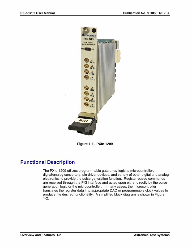
The PXIe-1209 (Figure 1-1) is a fully programmable, dual independent pulse generator that allows the generation of precisely-timed pulses of programmable frequency, pulse width, delay, and amplitude in two channels simultaneously. Each channel offers operational modes which include single, continuous, burst, and follow trigger functions. Single, double, and inverted pulses are supported. Extensive trigger and gating logic provide comprehensive control of pulse timing independently. Within each channel, the internal base clock can be disciplined to an external reference clock for long-term stability.
The PXIe-1209 can be used in a wide variety of applications including functional verification of digital systems, signal simulation, design verification, and research and development.
Key Features:
Dual Independent Channels
0.1 Hz – 100 MHz
Programmable Pulse Width, Pulse Delay, and Double Pulse Spacing
-1.5 V to +6.5 V Programmable Pulse Output
Programmable Rise/Fall Time
Single Pulse or Continuous Pulsing
Single Pulse, Double Pulse, and Inverted Pulse Modes
Burst Mode (1 to >2B pulses output on command or trigger)
Follow Trigger Mode
External Triggering
Asynchronous or Synchronous Gating Modes
On-board can be disciplined to 1 PPS, 100 PPS, or 10 MHz external clock for long-term stability
PXIe-1209 User Manual Publication No. 981050 REV. A
Overview and Features 1-2 Astronics Test Systems
Figure 1-1, PXIe-1209
Functional Description
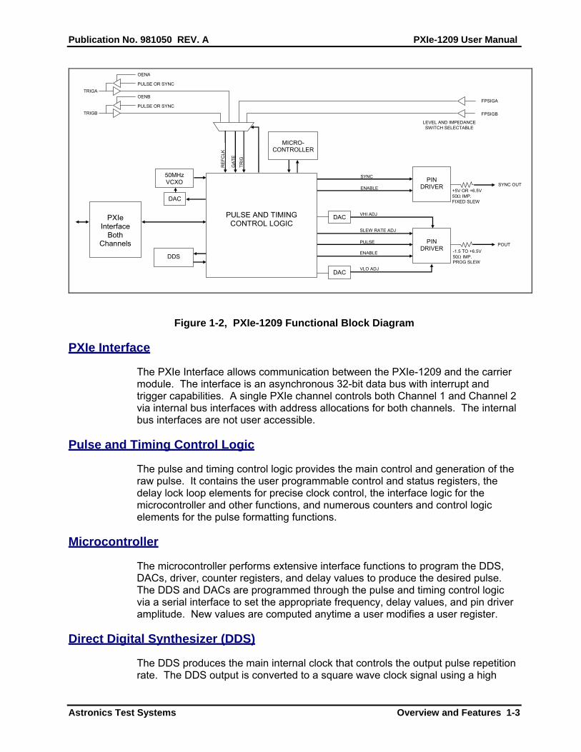
The PXIe-1209 utilizes programmable gate array logic, a microcontroller, digital/analog converters, pin driver devices, and variety of other digital and analog electronics to provide the pulse generation function. Register-based commands are received through the PXI interface and acted upon either directly by the pulse generation logic or the microcontroller. In many cases, the microcontroller translates the register data into appropriate DAC or programmable clock values to produce the desired functionality. A simplified block diagram is shown in Figure 1-2.
Publication No. 981050 REV. A PXIe-1209 User Manual
Astronics Test Systems Overview and Features 1-3
PULSE
ENABLE
SLEW RATE ADJ
VHI ADJ
VLO ADJ
SYNC OUT
PXIe
Interface Both
Channels
FPSIGB
FPSIGA
POUT
LEVEL AND IMPEDANCE SWITCH SELECTABLE
50MHz VCXO
DDS
PIN
DRIVER -1.5 TO +6.5V 50 IMP. PROG SLEW
+5V OR +6.5V 50 IMP. FIXED SLEW
TRIGA
TRIGB
GA
TE
TR
IG
ENABLE
SYNC
DAC
DAC
MICRO-CONTROLLER
DAC
PULSE OR SYNC
OENA
PULSE OR SYNC
OENB
PIN
DRIVER
PULSE AND TIMING CONTROL LOGIC
RE
FC
LK
Figure 1-2, PXIe-1209 Functional Block Diagram
PXIe Interface
The PXIe Interface allows communication between the PXIe-1209 and the carrier module. The interface is an asynchronous 32-bit data bus with interrupt and trigger capabilities. A single PXIe channel controls both Channel 1 and Channel 2 via internal bus interfaces with address allocations for both channels. The internal bus interfaces are not user accessible.
Pulse and Timing Control Logic
The pulse and timing control logic provides the main control and generation of the raw pulse. It contains the user programmable control and status registers, the delay lock loop elements for precise clock control, the interface logic for the microcontroller and other functions, and numerous counters and control logic elements for the pulse formatting functions.
Microcontroller
The microcontroller performs extensive interface functions to program the DDS, DACs, driver, counter registers, and delay values to produce the desired pulse. The DDS and DACs are programmed through the pulse and timing control logic via a serial interface to set the appropriate frequency, delay values, and pin driver amplitude. New values are computed anytime a user modifies a user register.
Direct Digital Synthesizer (DDS)
The DDS produces the main internal clock that controls the output pulse repetition rate. The DDS output is converted to a square wave clock signal using a high

PXIe-1209 User Manual Publication No. 981050 REV. A
Overview and Features 1-4 Astronics Test Systems
speed comparator.
VCXO
The voltage controlled oscillator (VCXO) provides the base clock for the module. Even though the internal VCXO is fairly accurate and stable on its own, it can also be disciplined to a high precision 1 PPS, 100 PPS, or 10 MHz external clock, if one is available.
Pin Drivers
The pin driver provides the output voltage, current, and slew rate of the output pulse and Sync Out signals. The output impedance of both pulses is fixed at 50 Ω.
Front Panel Input Signals
Two front panel trigger signals are provided for trigger, gate, or clock reference control from an external source. The inputs have switch selectable input impedance and threshold level control.
Backplane Trigger Signals
Four backplane PXI trigger signals are provided via trigger bus allocation via DLL drivers. As inputs, these signals can be used for external control of the trigger, gate, or clock reference. As outputs, they can be used to output the pulse and Sync Out signals. To utilize this feature, the PXI carrier must support triggers (third row on PXI interface). Trigger operation differs depending on the carrier; see your carrier’s documentation for details.
Operational Modes
The PXIe-1209 can be configured for many different operating modes. In order to fully understand the operation, it is important to have a clear understanding of the terminology used and relationship of the various signals as shown in Figure 1-3.

Publication No. 981050 REV. A PXIe-1209 User Manual
Astronics Test Systems Overview and Features 1-5
Figure 1-3, Pulse Terms and Relationships
Frequency (Pulse Repetition Rate)
The frequency of the output pulse can be controlled internally using the frequency value and mode registers or externally using an external trigger signal.
Pulse Width
The width of the output pulse can be controlled internally using the pulse width register or externally using an external trigger signal.
Pulse Delay and Double Pulse Spacing
The time from the Sync Out signal to the first output pulse and the space between the first pulse and second pulse, if Double Pulse is enabled, is programmable using the pulse delay and double pulse spacing registers.
Single Pulse or Double Pulse
The output pulse can be either a single or a double pulse. In Double Pulse mode, the widths of both pulses are the same.
Run Modes
There are four run modes: single, continuous, burst, and follow trigger. In all cases, except follow trigger, the output pulse can be a single pulse or a double pulse. The run event can be initiated by software or an external trigger. Single pulse mode produces one pulse (or a double pulse) for each software or trigger signal. Continuous mode continues pulsing until software disables the run. Burst mode allows a preset number of pulses to be produced. In the follow trigger mode, the output pulse follows both the pulse width and period of the trigger input.
PXIe-1209 User Manual Publication No. 981050 REV. A
Overview and Features 1-6 Astronics Test Systems
Pulse Output
The amplitude of the output pulse is programmable using the high and low level amplitude registers. The high level of the pulse and the low level of the pulse are controlled separately. The output can be enabled or disabled (placed in a high-impedance state) and the polarity (active-high or active-low) and slew rate are programmable. The output impedance is fixed at 50 Ω.
Sync Out
The Sync Out signal indicates the start (T0) of the pulse generation internal timing. The signal output can be enabled or disabled (placed in a high-impedance state) and its polarity (active-high or active-low) is programmable. The output level is switch selectable for 5.0 V or 6.5 V. The output impedance is fixed at 50 Ω.
External Trigger
An external signal can be used to control the pulse repetition rate, instead of the internal counter. Either the positive going or negative going transition can be used. Additionally, the output pulse can follow the pulse width and period of the trigger input signal.
External Gate
The module can be configured to enable pulsing only during the presence of an external signal. The gate operation can be asynchronous or synchronous (see Pulse Gating in Chapter 4 for details). The external gate can be active-high or active-low.
External Reference Clock
An external 1 PPS, 100 PPS, or 10 MHz signal can be used to discipline the internal clock. After an initial 10-minute module warm-up period, the internal clock will discipline in typically 30 seconds to within one decade of the external reference, up to the specified stability. Software register bits allow enabling the disciplining operation and provide status of the state of the reference and the internal clock.
Hardware Configuration
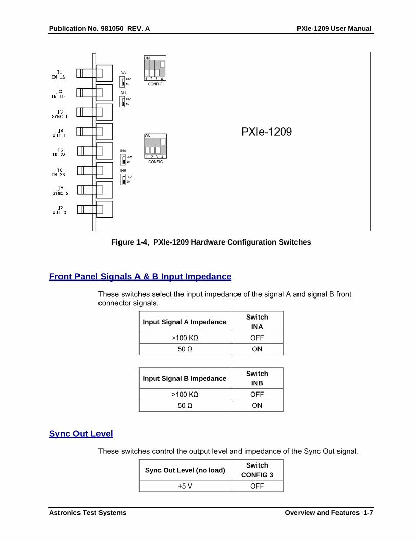
The PXIe-1209 contains three sets of four switches that select the input impedance of the FPSIGA and FPSIGB front panel inputs, the mode of operation for the pulse generation logic, and the Sync Out level and impedance. The switches are located as shown in Figure 1-4. The switches are only accessible with the module removed from the carrier.
Publication No. 981050 REV. A PXIe-1209 User Manual
Astronics Test Systems Overview and Features 1-7
Figure 1-4, PXIe-1209 Hardware Configuration Switches
Front Panel Signals A & B Input Impedance
These switches select the input impedance of the signal A and signal B front connector signals.
Input Signal A Impedance Switch
INA
>100 KΩ OFF
50 Ω ON
Input Signal B Impedance Switch
INB
>100 KΩ OFF
50 Ω ON
Sync Out Level
These switches control the output level and impedance of the Sync Out signal.
Sync Out Level (no load) Switch
CONFIG 3
+5 V OFF
PXIe-1209 User Manual Publication No. 981050 REV. A
Overview and Features 1-8 Astronics Test Systems
+6.5 V ON
Mode
These switches control special modes of operation. These modes are undefined at this time, but are available for future implementations with special purpose modes.
Special Mode 1 Switch
CONFIG 1
Normal OFF
Factory Debug Mode* ON
Special Mode 2 Switch
CONFIG 2
Undefined OFF
Undefined ON
CONFIG Switch 4 is not used.
Input/Output Signals
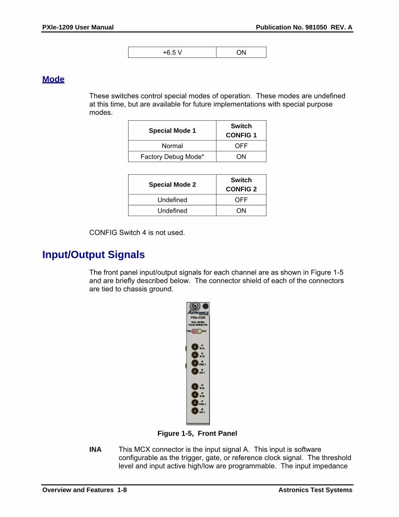
The front panel input/output signals for each channel are as shown in Figure 1-5 and are briefly described below. The connector shield of each of the connectors are tied to chassis ground.
Figure 1-5, Front Panel
INA This MCX connector is the input signal A. This input is software configurable as the trigger, gate, or reference clock signal. The threshold level and input active high/low are programmable. The input impedance
Publication No. 981050 REV. A PXIe-1209 User Manual
Astronics Test Systems Overview and Features 1-9
is switch selectable.
INB This MCX connector is the input signal B. This input is software configurable as the trigger, gate, or reference clock signal. The threshold level and input active high/low are programmable. The input impedance is switch selectable.
SYNC This MCX connector is the output Sync Out signal. The output level is switch selectable.
OUT This MCX connector is the output Pulse signal. The high and low levels are programmable.

Publication No. 981050 REV. A PXIe-1209 User Manual
Astronics Test Systems Specifications 2-1
Chapter 2
Specifications
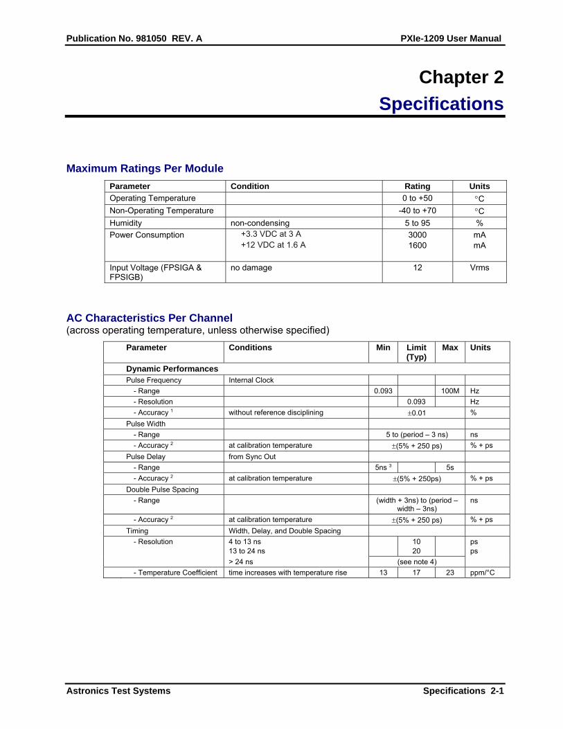
Maximum Ratings Per Module
Parameter Condition Rating Units
Operating Temperature 0 to +50 C
Non-Operating Temperature -40 to +70 C
Humidity non-condensing 5 to 95 %
Power Consumption +3.3 VDC at 3 A +12 VDC at 1.6 A
3000 1600
mA mA
Input Voltage (FPSIGA & FPSIGB)
no damage 12 Vrms
AC Characteristics Per Channel (across operating temperature, unless otherwise specified)
Parameter Conditions Min Limit (Typ)
Max Units
Dynamic Performances Pulse Frequency Internal Clock
- Range 0.093 100M Hz
- Resolution 0.093 Hz
- Accuracy 1 without reference disciplining 0.01 %
Pulse Width
- Range 5 to (period – 3 ns) ns
- Accuracy 2 at calibration temperature (5% + 250 ps) % + ps
Pulse Delay from Sync Out
- Range 5ns 3 5s
- Accuracy 2 at calibration temperature (5% + 250ps) % + ps
Double Pulse Spacing
- Range (width + 3ns) to (period – width – 3ns)
ns
- Accuracy 2 at calibration temperature (5% + 250 ps) % + ps
Timing Width, Delay, and Double Spacing
- Resolution 4 to 13 ns 13 to 24 ns
10 20
ps ps
> 24 ns (see note 4)
- Temperature Coefficient time increases with temperature rise 13 17 23 ppm/°C
PXIe-1209 User Manual Publication No. 981050 REV. A
Specifications 2-2 Astronics Test Systems
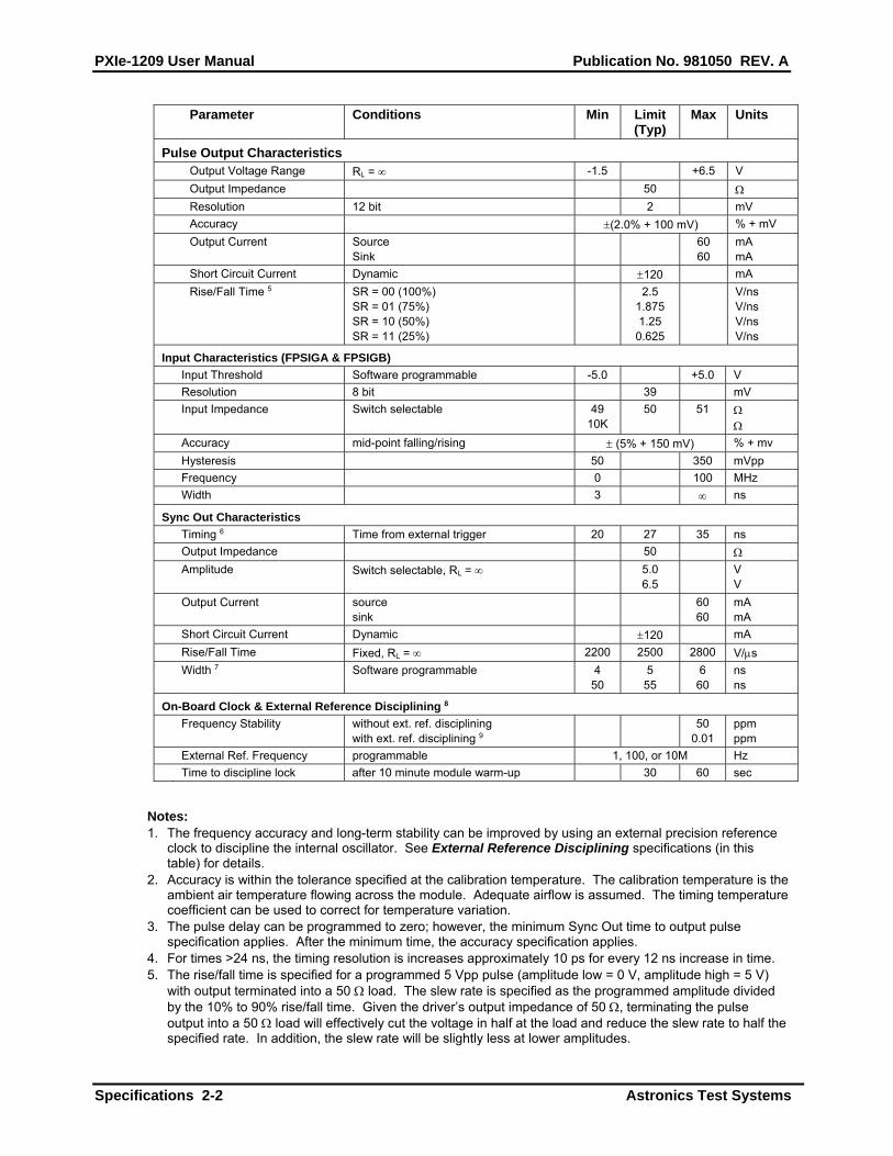
Parameter Conditions Min Limit (Typ)
Max Units
Pulse Output Characteristics Output Voltage Range RL = -1.5 +6.5 V
Output Impedance 50
Resolution 12 bit 2 mV
Accuracy (2.0% + 100 mV) % + mV
Output Current Source Sink
60 60
mA mA
Short Circuit Current Dynamic 120 mA
Rise/Fall Time 5
SR = 00 (100%) SR = 01 (75%) SR = 10 (50%) SR = 11 (25%)
2.5 1.875 1.25
0.625
V/ns V/ns V/ns V/ns
Input Characteristics (FPSIGA & FPSIGB)
Input Threshold Software programmable -5.0 +5.0 V
Resolution 8 bit 39 mV
Input Impedance Switch selectable
49 10K
50 51
Accuracy mid-point falling/rising (5% + 150 mV) % + mv
Hysteresis 50 350 mVpp
Frequency 0 100 MHz
Width 3 ns
Sync Out Characteristics
Timing 6 Time from external trigger 20 27 35 ns
Output Impedance 50
Amplitude Switch selectable, RL =
5.0 6.5
V V
Output Current source sink
60 60
mA mA
Short Circuit Current Dynamic 120 mA
Rise/Fall Time Fixed, RL = 2200 2500 2800 V/s
Width 7 Software programmable 4 50
5 55
6 60
ns ns
On-Board Clock & External Reference Disciplining 8
Frequency Stability without ext. ref. disciplining with ext. ref. disciplining 9
50 0.01
ppm ppm
External Ref. Frequency programmable 1, 100, or 10M Hz
Time to discipline lock after 10 minute module warm-up 30 60 sec
Notes: 1. The frequency accuracy and long-term stability can be improved by using an external precision reference
clock to discipline the internal oscillator. See External Reference Disciplining specifications (in this table) for details.
2. Accuracy is within the tolerance specified at the calibration temperature. The calibration temperature is the ambient air temperature flowing across the module. Adequate airflow is assumed. The timing temperature coefficient can be used to correct for temperature variation.
3. The pulse delay can be programmed to zero; however, the minimum Sync Out time to output pulse specification applies. After the minimum time, the accuracy specification applies.
4. For times >24 ns, the timing resolution is increases approximately 10 ps for every 12 ns increase in time. 5. The rise/fall time is specified for a programmed 5 Vpp pulse (amplitude low = 0 V, amplitude high = 5 V)
with output terminated into a 50 load. The slew rate is specified as the programmed amplitude divided by the 10% to 90% rise/fall time. Given the driver’s output impedance of 50 , terminating the pulse output into a 50 load will effectively cut the voltage in half at the load and reduce the slew rate to half the specified rate. In addition, the slew rate will be slightly less at lower amplitudes.
Publication No. 981050 REV. A PXIe-1209 User Manual
Astronics Test Systems Specifications 2-3
6. The Sync Out time specified is from the external front panel input to the external front panel Sync Out. Backplane triggering and Sync Out will vary depending on the carrier used.
7. When using long Sync Out, only the leading edge should be used to ensure low jitter to Pulse Out. The falling edge and hence the width of Sync Out varies up to 10 ns.
8. The on-board oscillator will discipline to within one decade of the external reference, up to the specified stability.
Mechanical
The mechanical dimensions of the module are in conformance with PXI Industry Standard per PXI Systems Alliance. The nominal dimensions are 160 mm long by 100 mm wide.
Bus Compliance
The module complies with the PXI Express Hardware Specification Revision 1.0.
Module Type: PXIe
Addressing: 32-bit
Data: D32
Interrupts Both Channels: INTA, INTB, INTC, and INTD
DMA: not supported
Triggers Per Channel: Input/Output Trig A and Trig B
Device ID: 120916
Vendor ID: 1D5D16
Class Code: 11000024
Revision ID 0A8
Sub System ID: 000116
SubSystem Vendor ID: 1D5D16
Environmental
Temperature/Altitude
Operating: 0° C to 55° C/10,000 ft
Storage: -40° C to 75° C/15,000 ft
Relative Humidity
5 to 95%, non–condensing <30° C
5 to 75%, non–condensing <40° C
Mechanical
Shock: 30 g, 11 ms, ½ sinewave
Vibration: 0.013 in (pk-pk), 5 to 55 Hz
Bench Handling: 4-inch drop at 45°
PXIe-1209 User Manual Publication No. 981050 REV. A
Specifications 2-4 Astronics Test Systems
CE Certifications
Emissions/Immunity: EN61326: 1997 + A1: 1998, Class A
Safety: EN61010-1: 1993 + A2: 1995
MTBF (MIL-HDBK-217 FN2, GB GC, 25°
379878 hrs
Mechanical
Weight
1.26 lbs (0.567 kg)
Dimensions
1 Slot Width PXI Express Module
Publication No. 981050 REV. A PXIe-1209 User Manual
Astronics Test Systems Installation 3-1
Chapter 3
Installation
Unpacking and Inspection
Verify that there has been no damage to the shipping container. If damage exists then the container should be retained, as it will provide evidence of carrier caused problems. Such problems should be reported to the shipping courier immediately, as well as to our Customer Support department. If there is no damage to the shipping container, carefully remove the module from its box and inspect for any signs of physical damage. If damage exists, report immediately to Astronics Customer Support.
Installing the Module into a PXIe Chassis
WARNING The PXIe-1209 module is NOT hot-swappable. The power to the PXIe chassis must be turned off before installing a PXIe-1209. Plugging the module in before the power is off may result in damage to the electronics.
The PXIe-1209 should be installed in any PXIe chassis hybrid or PXIe slot.
When inserting the module into the chassis, it should be gently rocked back and forth to seat the connectors into the backplane receptacles.
Software Installation
Prior to hardware installation of the PXIe-1209, install the following four software drivers:
1. VISA software, available from your PXI slot 0 device vendor
2. Windows PXI Device Driver (from LabVIEW driver installer)
3. LabWindows/CVI Instrument Driver (optional)
4. LabVIEW Instrument Driver (optional)
Note: You will need system administrator privileges to install these software items.
Installing the VISA driver
The LabVIEW and LabWindows/CVI driver communicate with the instrument using
PXIe-1209 User Manual Publication No. 981050 REV. A
Installation 3-2 Astronics Test Systems
the VISA software interface layer. The VISA software is provided by the manufacturer of your PXI controller. Obtain the VISA software from your PXI controller vendor, and follow their instructions for installing on your computer.
Installing the PXI device driver
The PXI Device Driver is included on both the LabWindows / CVI Instrument Driver Installer and the LabVIEW Instrument Driver Installer. You MUST install this driver so that the instrument will be properly recognized by Windows.
If you execute the LabVIEW Driver Installer, the PXI device driver is installed by default.
If you execute the LabWindows/CVI driver installer, the installer creates a subdirectory named “Windows Driver” inside the directory selected for installation. By default, on a 64-bit operating system, this directory will be:
C:\Program Files (x86)\IVI Foundation\VISA\WinNT\ri1209e
On a 32-bit operating system, the default would be:
C:\Program Files\IVI Foundation\VISA\WinNT\ri1209e
To install the PXI device driver:
1. Use the Windows explorer to navigate to the “Windows Driver” subdirectory.
2. Right-mouse click on the file “ri1209e.inf”.
3. Select “Install”.
Installing the LabVIEW instrument driver
1. Insert the install media disk into your computer.
2. Navigate to the “Drivers” folder on the install media.
3. Navigate to the LabVIEW Driver folder.
4. Double-click on the file “setup.exe”.
5. The driver installer will provide you with a choice for a standard or customer installation.
a. The standard installation will install the Windows PXI device driver for the 1209e. It will also install the driver for the version(s) of LabVIEW that is currently installed on your computer.
b. The customer installation allows you to select which version(s) of LabVIEW for which the driver will be installed. If you are running a version of LabVIEW that is not supported by the installer, you can select an older version of driver to use. For example, if you are running LabVIEW 2013, you can install the LabVIEW 2011 version and let LabVIEW re-compile the driver when it is first used.
6. The driver installer creates a directory “Astronics ri1209e” within the “instr.lib” subdirectory of the version of LabVIEW you are using.
Publication No. 981050 REV. A PXIe-1209 User Manual
Astronics Test Systems Installation 3-3
Installing the LabWindows/CVI instrument driver
1. Insert the install media disk into your computer.
2. Navigate to the “Drivers” folder on the install media.
3. Select the version of the installer that meets your needs.
a. Select the “InstallerWithRTE” folder if you do NOT have a version of the LabWindows/CVI run-time engine installed on your computer. The executable soft front panel requires the LabWindows/CVI run-time engine to work properly.
b. Select the “InstallerWithoutRTE” folder if you already have a version of the LabWindows/CVI run-time engine installed on your computer.
4. Double-click on the file “setup.exe”.
5. Follow the command prompts, and select the destination folder for installation.
6. By default, the installer will place the files within the VISA directory structure.
PXIe-1209 User Manual Publication No. 981050 REV. A
Installation 3-4 Astronics Test Systems
This page was left intentionally blank.

Publication No. 981050 REV. A PXIe-1209 User Manual
Astronics Test Systems Getting Started 4-1
Chapter 4
Operation
The PXIe-1209 is a register-based instrument that is controlled through a series of I/O registers described in Chapter 6. The exact method of accessing and addressing the I/O registers is dependent on the PXI carrier used to interface the module to your data acquisition or test system. Refer to the carrier’s documentation for information on the address mapping of a PXI’s I/O registers and to your system software documentation for details on data access.
Programming
NOTE: For most users, it is advisable to use either the LabWindows/CVI or the LabVIEW driver in your application development environment to program the PXIe-1209. Consult Chapter 5, Software Operation, of this manual for a description of how to use the software drivers supplied with this module
Writing Register Values
Normal 16-bit wide register values can be written in one write operation using 32-bit register access. However, some pulse parameters, such as the pulse period, pulse width, and pulse delay, require more than 16-bits. Special attention must be given when programming these values. To prevent a pulse parameter from changing until the entire value is written, the order of the write operations is important. The internal logic is configured to only accept the change when the high-order bits are written. Therefore, the application software must write the low bits first, then the middle bits, and lastly the high bits.
Pulse Programming
With the RUN bit disabled (0) in the Control/Status register, set the desired pulse frequency, pulse width, pulse delays, high/low amplitude, desired trigger control mode, pulse mode (single or double pulse), and run mode (single, continuous, burst, or follow trigger). After setting the desired pulse parameters, a finite amount of time (<20 ms) is required for configuration of the internal logic. The module will signal that it is ready to run by setting the RDY bit. Application software should verify the module is ready by reading the RDY bit. If desired, an interrupt can be generated to signal this event. Once the RDY bit is verified, enable the RUN bit (1). Modifications can be made to all settings except for RMODE without clearing the RUN bit; however, the RDY bit will go low momentarily and there may be a pulse glitch while the configuration is being adjusted.
Pulse Delay
The pulse delay is defined as the amount of time from the leading edge of Sync
PXIe-1209 User Manual Publication No. 981050 REV. A
Getting Started 4-2 Astronics Test Systems
Out to the leading edge of the output pulse. Pulse delay is user programmable from 5 ns to 5 seconds.
Sync Out
Sync Out marks the beginning of a single or double pulse sequence. The time from Sync Out to Pulse Out is user programmable from 5ns to 5 seconds. The width of Sync Out is programmable as short (~5 ns) or long (~50 ns). The short width should be used when pulsing at frequencies above 20 MHz. For frequencies less than 20 MHz, the short or long width can be used.
In addition, when using external triggering, it is important to keep in mind the time from external trigger to Sync Out time as specified in Sync Out in Chapter 1. This time is due to intrinsic propagation delays of the input circuitry and pulse generation logic. The time may vary from board to board, but will not vary significantly for a particular board.
In burst mode and when using synchronous gating, the time from the external trigger to Sync Out will jitter 5-10 ns from trigger to trigger, if the DDS/Divider Mode (FGM = 1) is being used (see Pulse and Timing Control Logic in Chapter 1 for more details). This is due to the required synchronization of the asynchronous external trigger to the internal clock on the PXIe-1209. Synchronization is not required when producing a Single or Double pulse sequence, so this jitter does not occur.
Frequency (Internal Pulse Repetition Rate)
The internal pulse repetition rate can be derived directly from the DDS output or controlled by a combination of the DDS output and a divider value. The direct DDS output should be used when producing continuous fixed frequency pulses, software initiated pulse burst, or asynchronous gating operations. This method allows the most flexible control and highest resolution of the frequency.
The combination of the DDS output and a divider value should be used when doing externally triggered pulse burst or synchronous gating operations. When using the divider, the DDS must be set to a frequency between 25 and 50 MHz. This clock is multiplied by four internally to provide a 100 to 200 MHz base clock for the input to the divider. The first pulse after an incoming external trigger or gate signal will occur synchronous to this base clock, which varies in period from 5 to 10ns, depending on the x4 internal clock frequency. If the direct DDS output were used, the pulse would be synchronous to that output clock, which may have a much longer period than 10 ns.
Single Pulse vs. Double Pulse
The DP bit in the Control/Status Register selects whether a single pulse (or double pulse) occurs when triggered. It is important to remember that the Double Pulse Spacing is the time from the rising edge of the first pulse to the rising edge of the second pulse; therefore, the Double Pulse Spacing must be set to a value greater than the Pulse Width.
Publication No. 981050 REV. A PXIe-1209 User Manual
Astronics Test Systems Getting Started 4-3
Single, Continuous, and Burst Modes
The RMODE bits in the Control/Status Register select whether a single pulse (or double pulse) or a series of pulses is output for each software run or external trigger. To output a continuous stream of pulses, set the RMODE to Continuous Cycle mode, then the RUN bit to 1. If the Trigger Source in the Trigger/Gate Control register is set to “Software RUN bit,” the pulses will start immediately. Otherwise, the pulse will start when the selected trigger becomes active. To stop the stream of pulses, set the RUN bit to 0. To output a specific number of pulses, set the Burst Count registers to the desired number, then set the RMODE to Burst mode. Use the software RUN bit or an external trigger to initiate the output of the desired number of pulses. The burst of pulses is outputed each time the RUN bit or external trigger go from inactive (0) to active (1). If desired, an interrupt can be generated at the end of the burst.
NOTE: Always set the RUN bit to 0 before changing the RMODE. Do not change the RMODE at the same time the RUN bit is changed (use separate write operations).
Follow Trigger Mode
Setting the RMODE bits in the Control/Status Register to “Follow Trigger Input” causes the output pulse to follow both the pulse width and period of the selected Trigger Source specified in the Trigger/Gate Control register. This feature can be used to provide level shifting of an input signal.
Pulse Gating
The pulse output can be gated to be present only during the active level of an external signal. To use this function, set the Gate Mode (GM) bit to a 1 in the Trigger/Gate Control register, the desired type of gating to synchronous or asynchronous using the SG bit, and select the gate source with the GATESEL bits.
With synchronous gating, the first pulse is synchronized with the rising edge of the gate signal. A pulse (or double pulse) will continue to be output as long as the gate signal is active when the Sync Out signal occurs.
With asynchronous gating, the pulse runs free internally, but will be low when the gate signal is inactive. The pulse output is not synchronized to the gate signal. Active pulses will only be present when the gate signal is active.
Calibration
Calibration values are used to adjust the timing accuracy for each of the delay elements, the pulse width, pulse delay, and double pulse spacing. These values should only be modified by trained factory personnel. The values can always be reset to Factory Default Values by setting the CRST bit in the first Calibration register. This bit resets all calibration values to their factory default values. Calibration is recommended every 12 months.

PXIe-1209 User Manual Publication No. 981050 REV. A
Getting Started 4-4 Astronics Test Systems
Reference Disciplining
The PXIe-1209’s internal oscillator can be disciplined to an external clock by selecting the reference clock source (REFSEL bits) in the control/status register. Enable disciplining and select the frequency of the input reference by setting the RFE bits (RFE1 and RFE0) in the control/status register. If a reference clock is detected, the DET bit in the control/status will be a one.
When the internal clock is disciplined to within approximately one decade of the reference clock, the LOK bit will transition high. If the module has warmed to a stable operating temperature, this typically requires around 30 seconds. The disciplining logic checks the internal clock frequency against the external reference clock every three seconds. If the module temperature is not stable, the disciplining logic may require longer to achieve lock and may transition out of lock. Since the purpose of reference disciplining is to achieve long term stability, occasional out of lock conditions are typically not detrimental. The disciplining status can be monitored by reading the Reference Count register. This register indicates the difference between the internal VCXO frequency and the external reference clock. The PXIe-1209 will continue to discipline itself to the reference clock as long as the reference clock is present. If the reference clock is removed, the PXIe-1209 will hold its internal clock at the disciplined frequency; however, normal drift will occur.
Reference Disciplining only affects the output frequency of the pulses. It does not affect the pulse width, pulse delay, or double pulse spacing accuracy.
Interrupts
The PXIe-1209 supports interrupts INTA, INTB, INTC, and INTD with allocations specified by the DLL driver.

Publication No. 981050 REV. A PXIe-1209 User Manual
Astronics Test Systems Operation 5-1
Chapter 5
Software Operation
Using the Soft Front Panel
The soft front panel allows the operator interactive control over the PXIe-1209 to allow instrument operation. All major functions are provided.
Starting the Soft Front Panel
The Soft Front Panel application is installed when you install the LabWindows / CVI driver. After the Soft Front Panel is installed, you may start it by selecting “Start -> All Programs -> VXIPNP -> Astronics Test Systems 1209e Dual Pulse Generator” from the task bar.
Figure 5-1, Starting Soft Front Panel
PXIe-1209 User Manual Publication No. 981050 REV. A
Operation 5-2 Astronics Test Systems
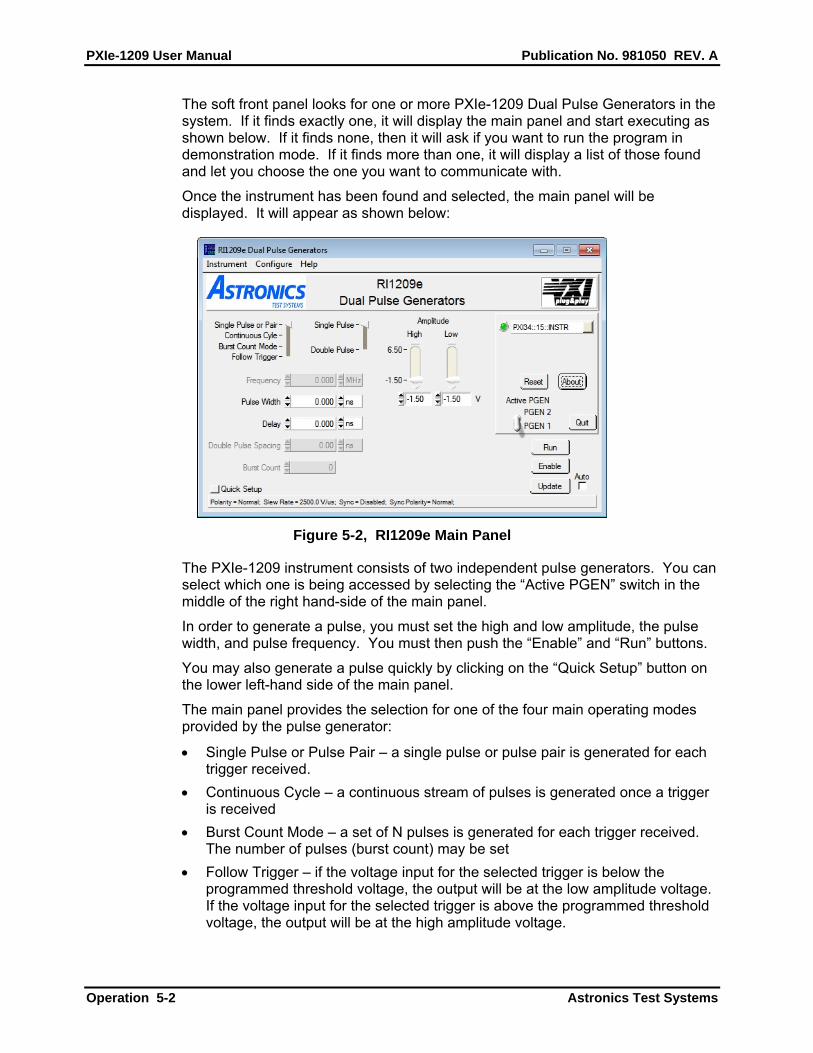
The soft front panel looks for one or more PXIe-1209 Dual Pulse Generators in the system. If it finds exactly one, it will display the main panel and start executing as shown below. If it finds none, then it will ask if you want to run the program in demonstration mode. If it finds more than one, it will display a list of those found and let you choose the one you want to communicate with.
Once the instrument has been found and selected, the main panel will be displayed. It will appear as shown below:
Figure 5-2, RI1209e Main Panel
The PXIe-1209 instrument consists of two independent pulse generators. You can select which one is being accessed by selecting the “Active PGEN” switch in the middle of the right hand-side of the main panel.
In order to generate a pulse, you must set the high and low amplitude, the pulse width, and pulse frequency. You must then push the “Enable” and “Run” buttons.
You may also generate a pulse quickly by clicking on the “Quick Setup” button on the lower left-hand side of the main panel.
The main panel provides the selection for one of the four main operating modes provided by the pulse generator:
Single Pulse or Pulse Pair – a single pulse or pulse pair is generated for each trigger received.
Continuous Cycle – a continuous stream of pulses is generated once a trigger is received
Burst Count Mode – a set of N pulses is generated for each trigger received. The number of pulses (burst count) may be set
Follow Trigger – if the voltage input for the selected trigger is below the programmed threshold voltage, the output will be at the low amplitude voltage. If the voltage input for the selected trigger is above the programmed threshold voltage, the output will be at the high amplitude voltage.
Publication No. 981050 REV. A PXIe-1209 User Manual
Astronics Test Systems Operation 5-3
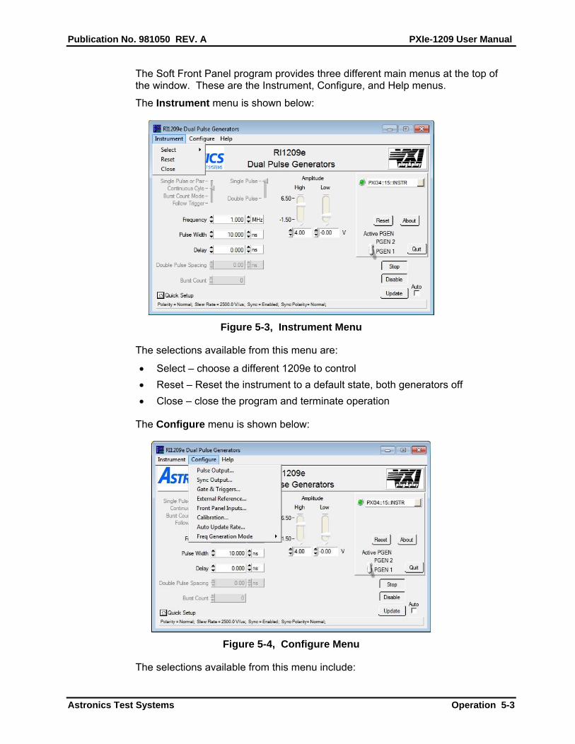
The Soft Front Panel program provides three different main menus at the top of the window. These are the Instrument, Configure, and Help menus.
The Instrument menu is shown below:
Figure 5-3, Instrument Menu
The selections available from this menu are:
Select – choose a different 1209e to control
Reset – Reset the instrument to a default state, both generators off
Close – close the program and terminate operation
The Configure menu is shown below:
Figure 5-4, Configure Menu
The selections available from this menu include:
PXIe-1209 User Manual Publication No. 981050 REV. A
Operation 5-4 Astronics Test Systems
Pulse Output – configure miscellaneous aspects about the output pulse
Sync Output – configure miscellaneous aspects for the Sync Output
Gate & Triggers – configure the gate and input triggers for the instrument
External Reference – select the external reference for the instrument
Front Panel Inputs – set the input thresholds for the front panel inputs
Calibration – provide the calibration interface for the module (NOTE: this is intended primarily for factory calibration and should generally not be changed by the end user)
Auto Update Rate – configure how often the main panel is refreshed
Frequency Generation Mode – select how the pulse frequency is generated
The Configure sub-menu items provide access to the various configurable aspects of the instrument that are not available via the main panel.
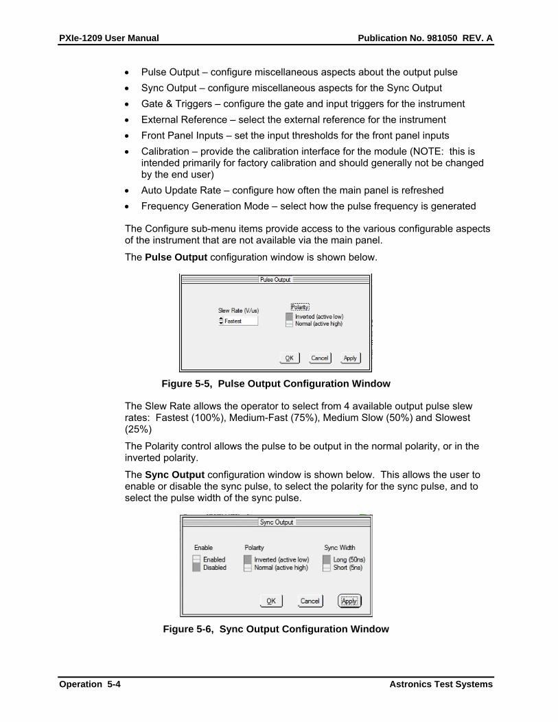
The Pulse Output configuration window is shown below.
Figure 5-5, Pulse Output Configuration Window
The Slew Rate allows the operator to select from 4 available output pulse slew rates: Fastest (100%), Medium-Fast (75%), Medium Slow (50%) and Slowest (25%)
The Polarity control allows the pulse to be output in the normal polarity, or in the inverted polarity.
The Sync Output configuration window is shown below. This allows the user to enable or disable the sync pulse, to select the polarity for the sync pulse, and to select the pulse width of the sync pulse.
Figure 5-6, Sync Output Configuration Window
Publication No. 981050 REV. A PXIe-1209 User Manual
Astronics Test Systems Operation 5-5
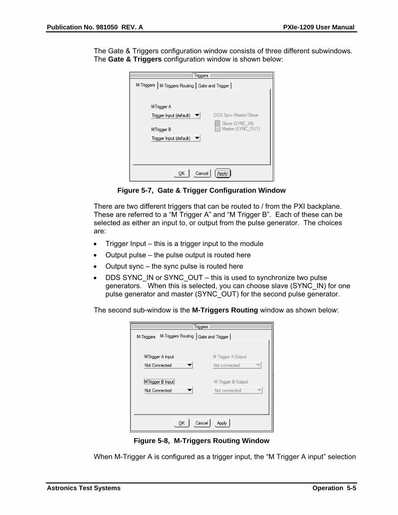
The Gate & Triggers configuration window consists of three different subwindows. The Gate & Triggers configuration window is shown below:
Figure 5-7, Gate & Trigger Configuration Window
There are two different triggers that can be routed to / from the PXI backplane. These are referred to a “M Trigger A” and “M Trigger B”. Each of these can be selected as either an input to, or output from the pulse generator. The choices are:
Trigger Input – this is a trigger input to the module
Output pulse – the pulse output is routed here
Output sync – the sync pulse is routed here
DDS SYNC_IN or SYNC_OUT – this is used to synchronize two pulse generators. When this is selected, you can choose slave (SYNC_IN) for one pulse generator and master (SYNC_OUT) for the second pulse generator.
The second sub-window is the M-Triggers Routing window as shown below:
Figure 5-8, M-Triggers Routing Window
When M-Trigger A is configured as a trigger input, the “M Trigger A input” selection
PXIe-1209 User Manual Publication No. 981050 REV. A
Operation 5-6 Astronics Test Systems
will be enabled. When it is configured as and output, the “M Trigger A Output” selection will be enabled. The same is true for M Trigger B.
The possible selections for M Trigger A input are:
Not Connected – default
PXI TRIG 0 – the input is connected to the PXI TRIG0 line (PGEN 1 only)
PXI TRIG 1 – the input is connected to the PXI TRIG1 line (PGEN 1 only)
PXI TRIG 4 – the input is connected to the PXI TRIG0 line (PGEN 2 only)
PXI TRIG 5 – the input is connected to the PXI TRIG1 line (PGEN 2 only)
Inter-trigger connect – the input is routed to an on-board trigger interconnection module, and so could be connected to M Trigger B output of this pulse generator or M Trigger A output or M Trigger B output of the alternate pulse generator.
PXI 10 MHz – the input is connected to the PXI 10 MHz clock
The possible selections for M Trigger A output are:
Not Connected – default
PXI TRIG 2 – the output is connected to the PXI TRIG2 line (PGEN 1 only)
PXI TRIG 6 – the output is connected to the PXI TRIG6 line (PGEN 2 only)
Inter-trigger connect – the output is routed to an on-board trigger interconnection module, and so could be connected to M Trigger B of this pulse generator or M Trigger A or M Trigger B of the alternate pulse generator.
The possible selections for M Trigger B input are:
Not Connected – default
PXI TRIG 0 – the input is connected to the PXI TRIG0 line (PGEN 1 only)
PXI TRIG 1 – the input is connected to the PXI TRIG1 line (PGEN 1 only)
PXI TRIG 4 – the input is connected to the PXI TRIG0 line (PGEN 2 only)
PXI TRIG 5 – the input is connected to the PXI TRIG1 line (PGEN 2 only)
Inter-trigger connect – the input is routed to an on-board trigger interconnection module, and so could be connected to M Trigger A output of this pulse generator or M Trigger A output or M Trigger B output of the alternate pulse generator.
PXI 10 MHz – the input is connected to the PXI 10 MHz clock
The possible selections for M Trigger B output are:
Not Connected – default
PXI TRIG 3 – the output is connected to the PXI TRIG3 line (PGEN 1 only)
PXI TRIG 7 – the output is connected to the PXI TRIG7 line (PGEN 1 only)
Inter-trigger connect – the output is routed to an on-board trigger interconnection module, and so could be connected to M Trigger A of this pulse generator or M Trigger A or M Trigger B of the alternate pulse generator.
Publication No. 981050 REV. A PXIe-1209 User Manual
Astronics Test Systems Operation 5-7
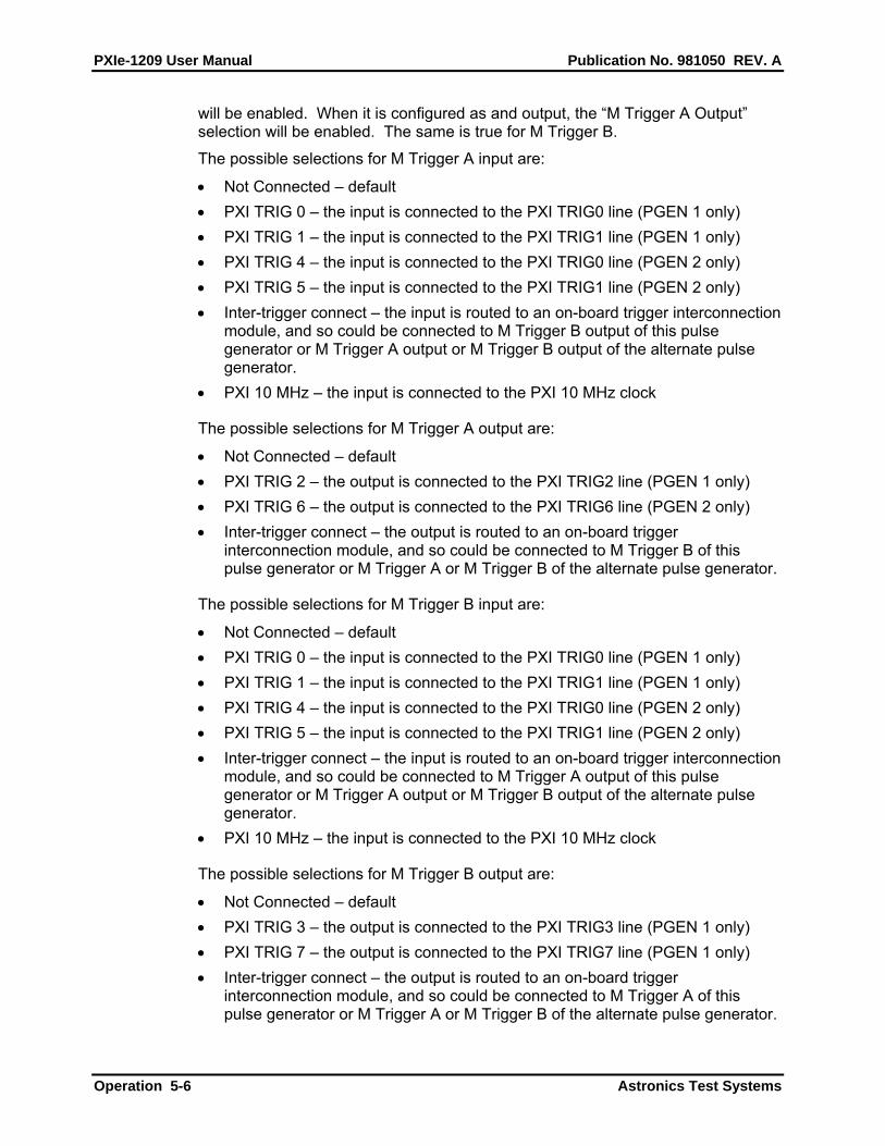
The Gate and Trigger subwindow is shown below:
Figure 5-9, Gate and Trigger Subwindow
This window allows the user to enable or disable the gate operation for the pulse generator. It also allows the user to select whether the gate mode is synchronous or asynchronous. In addition, it allows the user to select which input acts as the gate and which input acts as the trigger.
The gate input selection options are:
Ignore gate – same as setting the gate to disabled
Front Panel signal A (high level). A high level on the IN 1 A input (for PGEN #1) or IN 2 A input (for PGEN #2) enables the pulse output. A high level means that the voltage at the input is above the programmed threshold by the “Input A threshold” setting of the “Front Panel Inputs” configuration window.
Front Panel signal A (low level). A low level on the IN 1 A input (for PGEN #1) or IN 2 A input (for PGEN #2) enables the pulse output. A low level means that the voltage at the input is below the programmed threshold by the “Input A threshold” setting of the “Front Panel Inputs” configuration window.
Front Panel signal B (high level). A high level on the IN 1 B input (for PGEN #1) or IN 2 B input (for PGEN #2) enables the pulse output. A high level means that the voltage at the input is above the programmed threshold by the “Input B threshold” setting of the “Front Panel Inputs” configuration window.
Front Panel signal B (low level). A low level on the IN 1 B input (for PGEN #1) or IN 2 B input (for PGEN #2) enables the pulse output. A low level means that the voltage at the input is below the programmed threshold by the “Input B threshold” setting of the “Front Panel Inputs” configuration window.
Backplane Trigger A (high level). A logic 1 level on the currently selected M Trigger A input enables the pulse.
Backplane Trigger A (low level). A logic 0 level on the currently selected M Trigger A input enables the pulse.
Backplane Trigger B (high level). A logic 1 level on the currently selected M Trigger B input enables the pulse.

PXIe-1209 User Manual Publication No. 981050 REV. A
Operation 5-8 Astronics Test Systems
Backplane Trigger B (low level). A logic 0 level on the currently selected M Trigger B input enables the pulse.
The trigger input selections are:
Software Run Bit (default) – the pulse is generated immediately when the RUN and ENABLE buttons on the front panel are set.
Front Panel Signal A (rising edge) – An input signal which crosses the programmed “Input A Threshold” with a rising edge on the IN 1 A input (for PGEN #1) or IN 2 A input (for PGEN #2) triggers the pulse generator.
Front Panel Signal A (falling edge) – An input signal which crosses the programmed “Input A Threshold” with a falling edge on the IN 1 A input (for PGEN #1) or IN 2 A input (for PGEN #2) triggers the pulse generator.
Front Panel Signal B (rising edge) – An input signal which crosses the programmed “Input B Threshold” with a rising edge on the IN 1 B input (for PGEN #1) or IN 2 B input (for PGEN #2) triggers the pulse generator.
Front Panel Signal B (falling edge) – An input signal which crosses the programmed “Input B Threshold” with a falling edge on the IN 1 B input (for PGEN #1) or IN 2 B input (for PGEN #2) triggers the pulse generator.
Front Panel Signal A (rising edge) – An input signal which crosses the programmed “Input A Threshold” with a rising edge on the IN 1 A input (for PGEN #1) or IN 2 A input (for PGEN #2) triggers the pulse generator.
Backplane Trigger A (rising edge) – A rising edge of the signal that is presently selected input for M Trigger A triggers the pulse generator.
Backplane Trigger A (falling edge) – A falling edge of the signal that is presently selected input for M Trigger B triggers the pulse generator.
Backplane Trigger B (rising edge) – A rising edge of the signal that is presently selected input for M Trigger B triggers the pulse generator.
Backplane Trigger B (falling edge) – A falling edge of the signal that is presently selected input for M Trigger B triggers the pulse generator.
The External Reference configuration window is shown below. This window allows the external reference to be enabled or disabled. When enabled, it provides the means to select the reference frequency (1 PPS, 100 PPS, or 10 MHz), and the external reference source (Front Panel Signal A, Front Panel Signal B, Backplane Trigger A, or Backplane Trigger B).
Figure 5-10, External Reference Configuration Window
Publication No. 981050 REV. A PXIe-1209 User Manual
Astronics Test Systems Operation 5-9
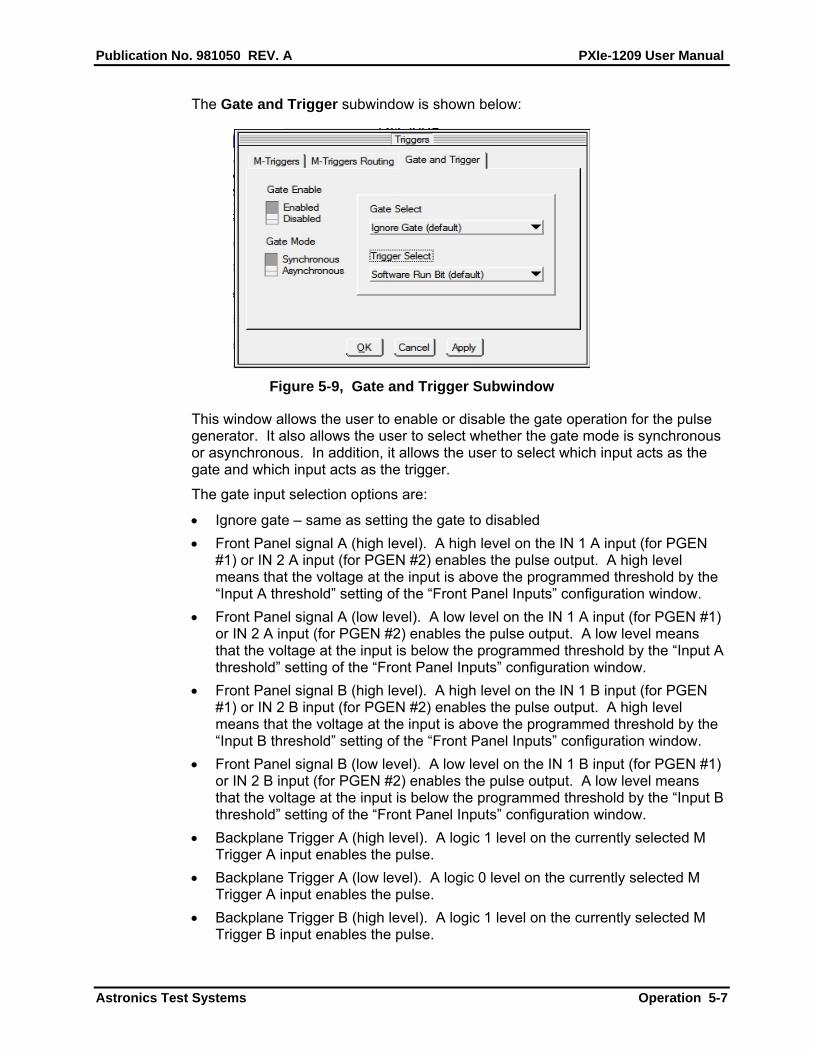
The Front Panel Inputs configuration window is shown below:
Figure 5-11, Front Panel Inputs Configuration Window
This window provides the ability to program the input thresholds for the IN 1 A and IN 1 B front panel inputs (for PGEN 1) or the IN 2 A and IN 2 B front panel inputs (for PGEN 2). It also allows the user to set the hysteresis voltage. This panel provides the means to set the threshold DACs directly, but that feature is generally used for calibration and / or troubleshooting and is generally not needed.
The Calibration window is not shown as this is intended for use primarily for factory calibration.
The Auto-Update window allows the user to set how often the main front panel is refreshed. In order for this value to have any effect, the “Auto” checkbox on the main front panel, next to the “Update” button, must be checked.
The Frequency Generation Mode menu item allows the user to select how the pulse frequency is derived. It may be “Auto”, “DDS”, or “DDS and Divider”. In general, this should be left in “Auto” mode.
Using the LabWindows / CVI Driver
The LabWindows / CVI driver provides a ‘C’ language programming interface. This driver also includes a 32-bit and 64-bit DLL that can be used within various programming environments such as Microsoft Visual Studio C++ and C#.
The first step to using any of the functions in the driver is to call the “ri1209e_init()” function. This function takes the VISA descriptor that identifies which instrument is being accessed and returns a “handle”. All of the other functions in the driver use this handle.
The last step in using the driver is to call the “ri1209e_close()” function. Each time you make a call to the “ri1209e_init()” function, it returns a new handle and allocates some memory for that driver session. Calling the “ri1209e_close()” functions releases the memory and resources associated with the handle.
PXIe-1209 User Manual Publication No. 981050 REV. A
Operation 5-10 Astronics Test Systems
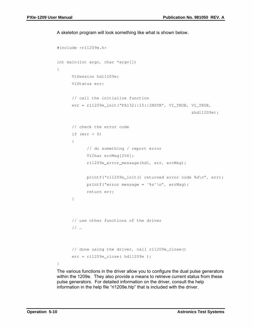
A skeleton program will look something like what is shown below.
#include <ri1209e.h>
int main(int argc, char *argv[])
ViSession hdl1209e;
ViStatus err;
// call the initialize function
err = ri1209e_init(“PXI32::15::INSTR”, VI_TRUE, VI_TRUE,
&hdl1209e);
// check the error code
if (err < 0)
// do something / report error
ViChar errMsg[256];
ri1209e_error_message(hdl, err, errMsg);
printf(“ri1209e_init() returned error code %d\n”, err);
printf(“error message = ‘%s’\n”, errMsg);
return err;
// use other functions of the driver
// …
// done using the driver, call ri1209e_close()
err = ri1209e_close( hdl1209e );
The various functions in the driver allow you to configure the dual pulse generators within the 1209e. They also provide a means to retrieve current status from these pulse generators. For detailed information on the driver, consult the help information in the help file “ri1209e.hlp” that is included with the driver.

Publication No. 981050 REV. A PXIe-1209 User Manual
Astronics Test Systems Operation 5-11
Using the LabVIEW Driver
The LabVIEW driver provides the means to control and interact with the PXIe-1209 from within the National Instruments LabVIEW programming environment.
The first step in using any of the VIs in the LabVIEW driver is to initialize the instrument using the “ri1209e Initialize.vi”. You can select this from within a LabVIEW diagram by right-mouse clicking and selecting
Instrument I/O -> Instr Drivers -> Astronics ri1209e ->ri1209e Initialize.vi
Once in the diagram, the VI must be supplied with the instrument descriptor for the 1209e. This will be assigned by the VISA software provided by the PXI controller. A typical instrument descriptor is “PXI34::15::INSTR”.
A rudimentary VI block diagram with just the ri1209e Intiialize.vi is shown in the next figure.
This next VI illustration shows that the instrument descriptor has been selected and wired into the VI.
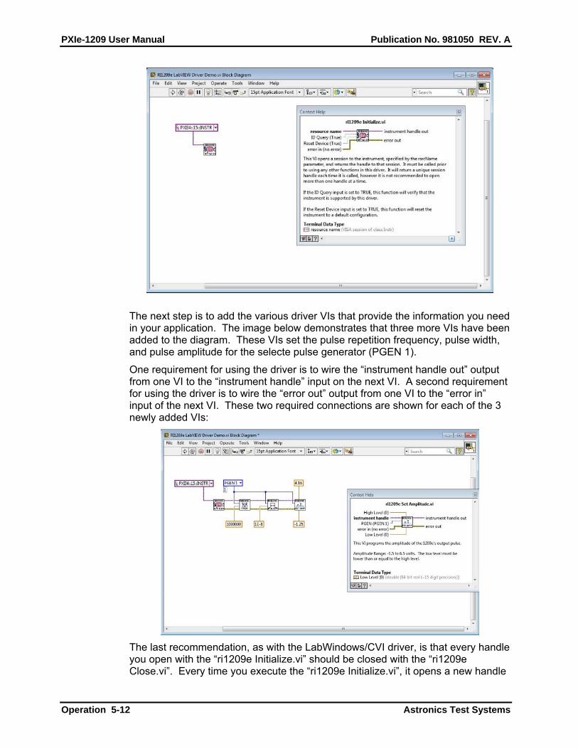
PXIe-1209 User Manual Publication No. 981050 REV. A
Operation 5-12 Astronics Test Systems
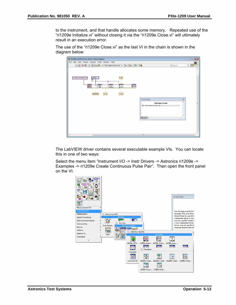
The next step is to add the various driver VIs that provide the information you need in your application. The image below demonstrates that three more VIs have been added to the diagram. These VIs set the pulse repetition frequency, pulse width, and pulse amplitude for the selecte pulse generator (PGEN 1).
One requirement for using the driver is to wire the “instrument handle out” output from one VI to the “instrument handle” input on the next VI. A second requirement for using the driver is to wire the “error out” output from one VI to the “error in” input of the next VI. These two required connections are shown for each of the 3 newly added VIs:
The last recommendation, as with the LabWindows/CVI driver, is that every handle you open with the “ri1209e Initialize.vi” should be closed with the “ri1209e Close.vi”. Every time you execute the “ri1209e Initialize.vi”, it opens a new handle
Publication No. 981050 REV. A PXIe-1209 User Manual
Astronics Test Systems Operation 5-13
to the instrument, and that handle allocates some memory. Repeated use of the “ri1209e Initialize.vi” without closing it via the “ri1209e Close.vi” will ultimately result in an execution error.
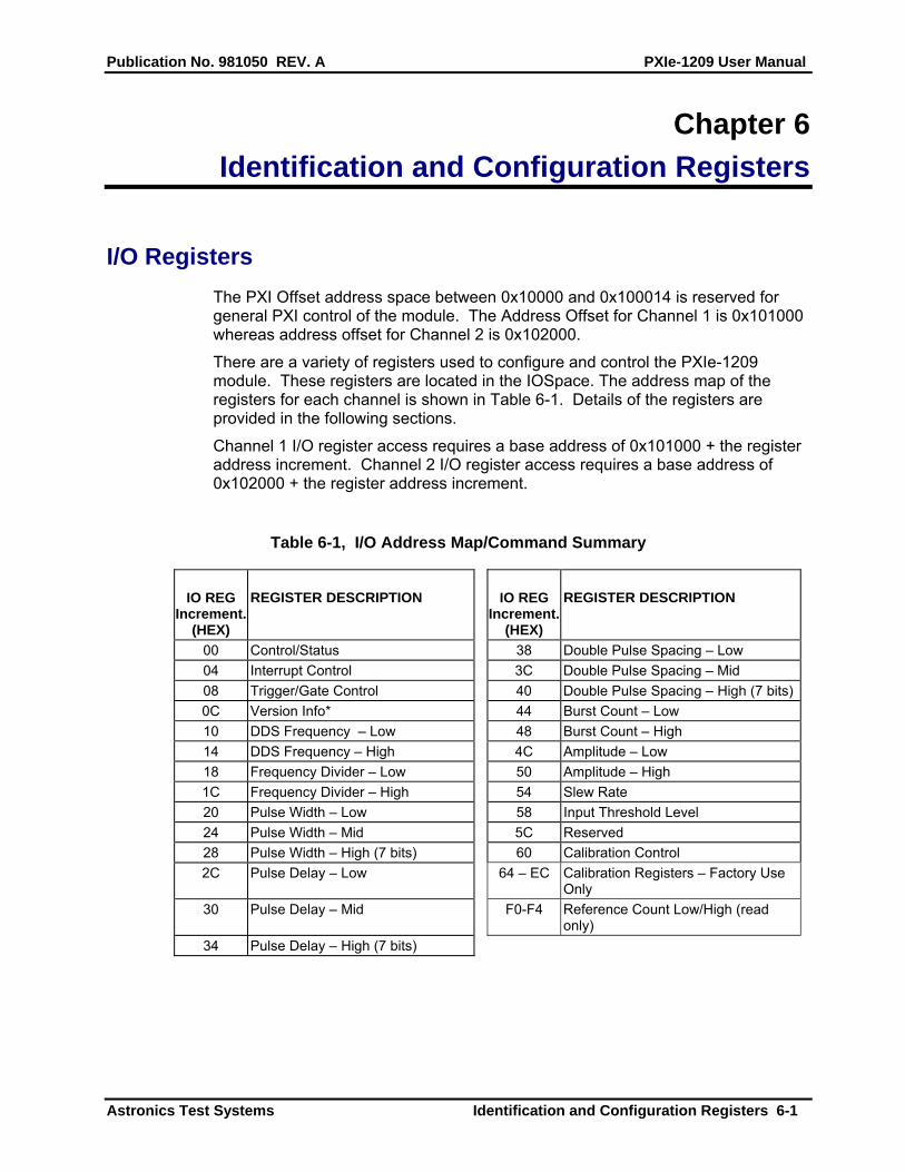
The use of the “ri1209e Close.vi” as the last VI in the chain is shown in the diagram below:
The LabVIEW driver contains several executable example VIs. You can locate this in one of two ways:
Select the menu item “Instrument I/O -> Instr Drivers -> Astronics ri1209e -> Examples -> ri1209e Create Continuous Pulse Pair”. Then open the front panel on the VI.

PXIe-1209 User Manual Publication No. 981050 REV. A
Operation 5-14 Astronics Test Systems
Alternatively, from the LabVIEW menu of any front panel, you can select “Help -> Find Examples…”. This will launch the NI Example Finder. From there, you can look under the “instruments” folder and select the “ri1209e Create Continuous Pulse Pair.vi”.
You may find full help information on the driver by selecting the “Help -> Astronics ri1209e -> ri1209e LabVIEW Help” menu item from any VI’s front panel.
Publication No. 981050 REV. A PXIe-1209 User Manual
Astronics Test Systems Identification and Configuration Registers 6-1
Chapter 6
Identification and Configuration Registers
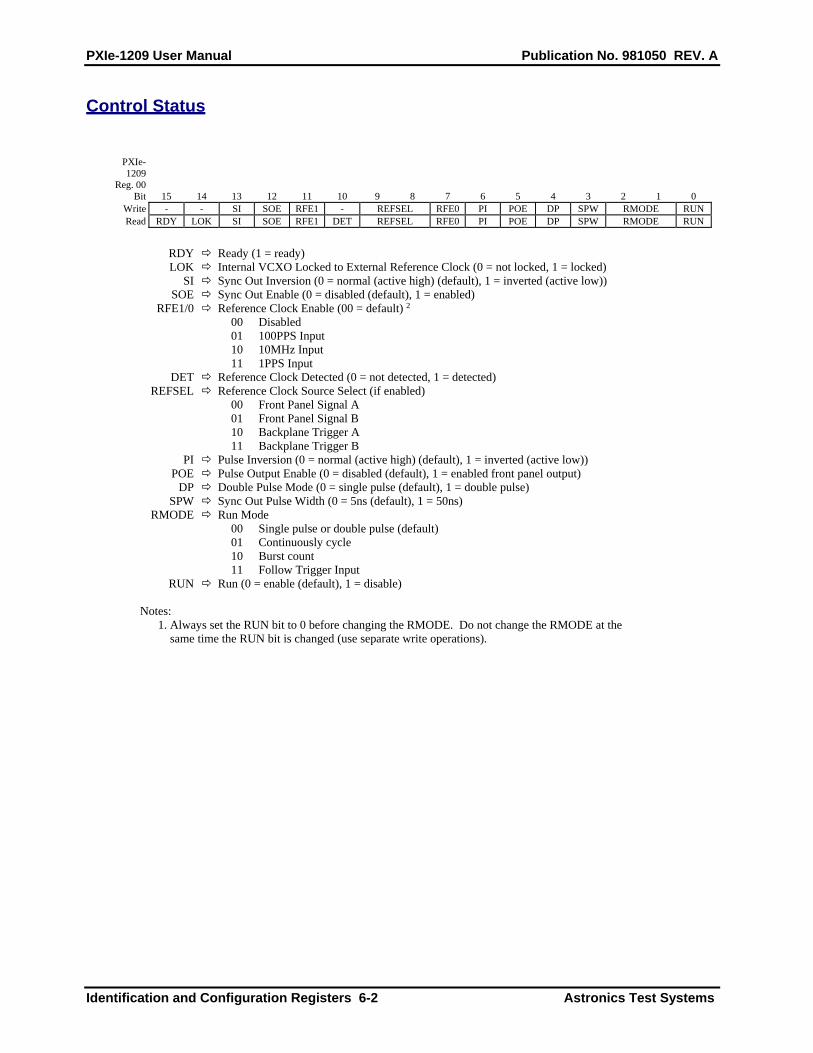
I/O Registers
The PXI Offset address space between 0x10000 and 0x100014 is reserved for general PXI control of the module. The Address Offset for Channel 1 is 0x101000 whereas address offset for Channel 2 is 0x102000.
There are a variety of registers used to configure and control the PXIe-1209 module. These registers are located in the IOSpace. The address map of the registers for each channel is shown in Table 6-1. Details of the registers are provided in the following sections.
Channel 1 I/O register access requires a base address of 0x101000 + the register address increment. Channel 2 I/O register access requires a base address of 0x102000 + the register address increment.
Table 6-1, I/O Address Map/Command Summary
IO REG
Increment. (HEX)
REGISTER DESCRIPTION
IO REG
Increment. (HEX)
REGISTER DESCRIPTION
00 Control/Status 38 Double Pulse Spacing – Low
04 Interrupt Control 3C Double Pulse Spacing – Mid
08 Trigger/Gate Control 40 Double Pulse Spacing – High (7 bits)
0C Version Info* 44 Burst Count – Low
10 DDS Frequency – Low 48 Burst Count – High
14 DDS Frequency – High 4C Amplitude – Low
18 Frequency Divider – Low 50 Amplitude – High
1C Frequency Divider – High 54 Slew Rate
20 Pulse Width – Low 58 Input Threshold Level
24 Pulse Width – Mid 5C Reserved
28 Pulse Width – High (7 bits) 60 Calibration Control
2C Pulse Delay – Low 64 – EC Calibration Registers – Factory Use Only
30 Pulse Delay – Mid F0-F4 Reference Count Low/High (read only)
34 Pulse Delay – High (7 bits)
PXIe-1209 User Manual Publication No. 981050 REV. A
Identification and Configuration Registers 6-2 Astronics Test Systems
Control Status
PXIe-1209
Reg. 00
Bit 15 14 13 12 11 10 9 8 7 6 5 4 3 2 1 0 Write - - SI SOE RFE1 - REFSEL RFE0 PI POE DP SPW RMODE RUN Read RDY LOK SI SOE RFE1 DET REFSEL RFE0 PI POE DP SPW RMODE RUN
RDY Ready (1 = ready) LOK Internal VCXO Locked to External Reference Clock (0 = not locked, 1 = locked) SI Sync Out Inversion (0 = normal (active high) (default), 1 = inverted (active low)) SOE Sync Out Enable (0 = disabled (default), 1 = enabled) RFE1/0 Reference Clock Enable (00 = default) 2
00 Disabled 01 100PPS Input 10 10MHz Input 11 1PPS Input
DET Reference Clock Detected (0 = not detected, 1 = detected) REFSEL Reference Clock Source Select (if enabled)
00 Front Panel Signal A 01 Front Panel Signal B 10 Backplane Trigger A 11 Backplane Trigger B
PI Pulse Inversion (0 = normal (active high) (default), 1 = inverted (active low)) POE Pulse Output Enable (0 = disabled (default), 1 = enabled front panel output) DP Double Pulse Mode (0 = single pulse (default), 1 = double pulse) SPW Sync Out Pulse Width (0 = 5ns (default), 1 = 50ns) RMODE Run Mode
00 Single pulse or double pulse (default) 01 Continuously cycle 10 Burst count 11 Follow Trigger Input
RUN Run (0 = enable (default), 1 = disable) Notes: 1. Always set the RUN bit to 0 before changing the RMODE. Do not change the RMODE at the
same time the RUN bit is changed (use separate write operations).
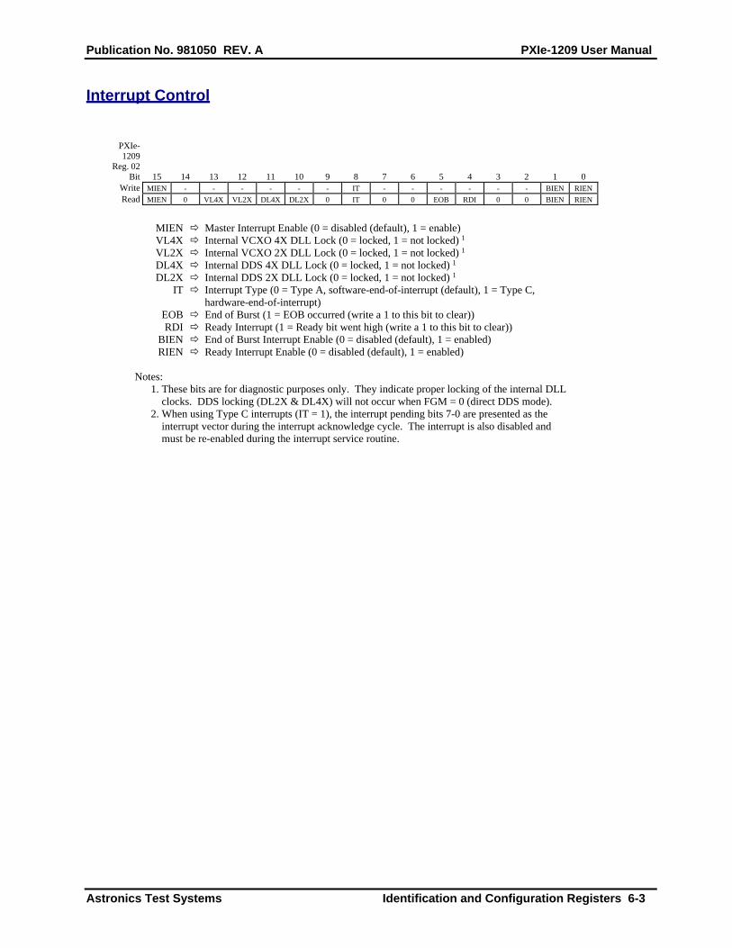
Publication No. 981050 REV. A PXIe-1209 User Manual
Astronics Test Systems Identification and Configuration Registers 6-3
Interrupt Control
PXIe-1209
Reg. 02
Bit 15 14 13 12 11 10 9 8 7 6 5 4 3 2 1 0 Write MIEN - - - - - - IT - - - - - - BIEN RIEN
Read MIEN 0 VL4X VL2X DL4X DL2X 0 IT 0 0 EOB RDI 0 0 BIEN RIEN
MIEN Master Interrupt Enable (0 = disabled (default), 1 = enable) VL4X Internal VCXO 4X DLL Lock (0 = locked, 1 = not locked) 1 VL2X Internal VCXO 2X DLL Lock (0 = locked, 1 = not locked) 1 DL4X Internal DDS 4X DLL Lock (0 = locked, 1 = not locked) 1 DL2X Internal DDS 2X DLL Lock (0 = locked, 1 = not locked) 1 IT Interrupt Type (0 = Type A, software-end-of-interrupt (default), 1 = Type C,
hardware-end-of-interrupt) EOB End of Burst (1 = EOB occurred (write a 1 to this bit to clear)) RDI Ready Interrupt (1 = Ready bit went high (write a 1 to this bit to clear)) BIEN End of Burst Interrupt Enable (0 = disabled (default), 1 = enabled) RIEN Ready Interrupt Enable (0 = disabled (default), 1 = enabled) Notes: 1. These bits are for diagnostic purposes only. They indicate proper locking of the internal DLL
clocks. DDS locking (DL2X & DL4X) will not occur when FGM = 0 (direct DDS mode). 2. When using Type C interrupts (IT = 1), the interrupt pending bits 7-0 are presented as the
interrupt vector during the interrupt acknowledge cycle. The interrupt is also disabled and must be re-enabled during the interrupt service routine.
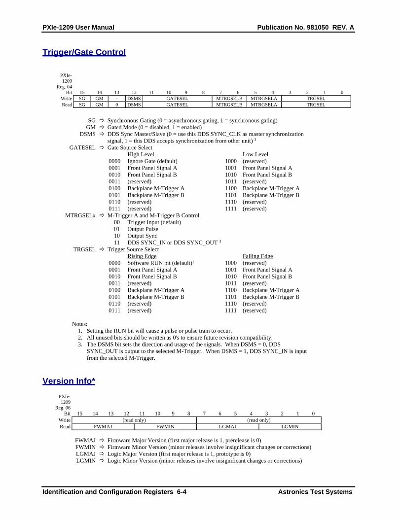
PXIe-1209 User Manual Publication No. 981050 REV. A
Identification and Configuration Registers 6-4 Astronics Test Systems
Trigger/Gate Control
PXIe-1209
Reg. 04
Bit 15 14 13 12 11 10 9 8 7 6 5 4 3 2 1 0 Write SG GM - DSMS GATESEL MTRGSELB MTRGSELA TRGSEL Read SG GM 0 DSMS GATESEL MTRGSELB MTRGSELA TRGSEL
SG Synchronous Gating (0 = asynchronous gating, 1 = synchronous gating) GM Gated Mode (0 = disabled, 1 = enabled) DSMS DDS Sync Master/Slave (0 = use this DDS SYNC_CLK as master synchronization
signal, 1 = this DDS accepts synchronization from other unit) 3 GATESEL Gate Source Select
High Level Low Level 0000 Ignore Gate (default) 1000 (reserved) 0001 Front Panel Signal A 1001 Front Panel Signal A 0010 Front Panel Signal B 1010 Front Panel Signal B 0011 (reserved) 1011 (reserved) 0100 Backplane M-Trigger A 1100 Backplane M-Trigger A 0101 Backplane M-Trigger B 1101 Backplane M-Trigger B 0110 (reserved) 1110 (reserved) 0111 (reserved) 1111 (reserved)
MTRGSELx M-Trigger A and M-Trigger B Control 00 Trigger Input (default) 01 Output Pulse 10 Output Sync 11 DDS SYNC_IN or DDS SYNC_OUT 3
TRGSEL Trigger Source Select Rising Edge Falling Edge 0000 Software RUN bit (default)1 1000 (reserved) 0001 Front Panel Signal A 1001 Front Panel Signal A 0010 Front Panel Signal B 1010 Front Panel Signal B 0011 (reserved) 1011 (reserved) 0100 Backplane M-Trigger A 1100 Backplane M-Trigger A 0101 Backplane M-Trigger B 1101 Backplane M-Trigger B 0110 (reserved) 1110 (reserved) 0111 (reserved) 1111 (reserved)
Notes: 1. Setting the RUN bit will cause a pulse or pulse train to occur. 2. All unused bits should be written as 0's to ensure future revision compatibility. 3. The DSMS bit sets the direction and usage of the signals. When DSMS = 0, DDS
SYNC_OUT is output to the selected M-Trigger. When DSMS = 1, DDS SYNC_IN is input from the selected M-Trigger.
Version Info*
PXIe-1209
Reg. 06
Bit 15 14 13 12 11 10 9 8 7 6 5 4 3 2 1 0 Write (read only) (read only) Read FWMAJ FWMIN LGMAJ LGMIN
FWMAJ Firmware Major Version (first major release is 1, prerelease is 0) FWMIN Firmware Minor Version (minor releases involve insignificant changes or corrections) LGMAJ Logic Major Version (first major release is 1, prototype is 0) LGMIN Logic Minor Version (minor releases involve insignificant changes or corrections)

Publication No. 981050 REV. A PXIe-1209 User Manual
Astronics Test Systems Identification and Configuration Registers 6-5
DDS Frequency - Low
PXIe-1209
Reg.08
Bit 15 14 13 12 11 10 9 8 7 6 5 4 3 2 1 0 Write 15 Low Order Bits 0 Read 15 Low Order Bits 0
DDS Frequency - High
PXIe-1209
Reg.0A
Bit 15 14 13 12 11 10 9 8 7 6 5 4 3 2 1 0 Write 31 High Order Bits 16 Read 31 High Order Bits 16
Notes:
1. Each bit represents ~0.093Hz (use 400MHz (232 – 1) for programming). 2. When FGM = 1 (frequency divider mode), the frequency must be set to a value 25MHz and
50MHz. 3. The registers must be written in the order low then high. The new frequency divider value
does not take effect until the high order register is written.
Frequency Divider – Low
PXIe-1209
Reg.0C
Bit 15 14 13 12 11 10 9 8 7 6 5 4 3 2 1 0 Write 15 Low Order Bits 0 Read 15 Low Order Bits 0
Frequency Divider – High
PXIe-1209
Reg.0E
Bit 15 14 13 12 11 10 9 8 7 6 5 4 3 2 1 0 Write FGM - 29 High Order Bits 16 Read FGM 0 29 High Order Bits 16
FGM Frequency Generation Mode (0 = DDS output directly controls the pulse
frequency (default), 1 = pulse frequency is controlled by a combination of the DDS output and a divider value)
Notes:
1. These registers are only used when the FGM bit the Frequency Mode Control register is set. 2. The pulse frequency is equal to (DDS Frequency 4) Frequency Divider value. 3. The minimum divider value is two (2). 4. The registers must be written in the order low then high. The new frequency divider value
does not take effect until the high order register is written.
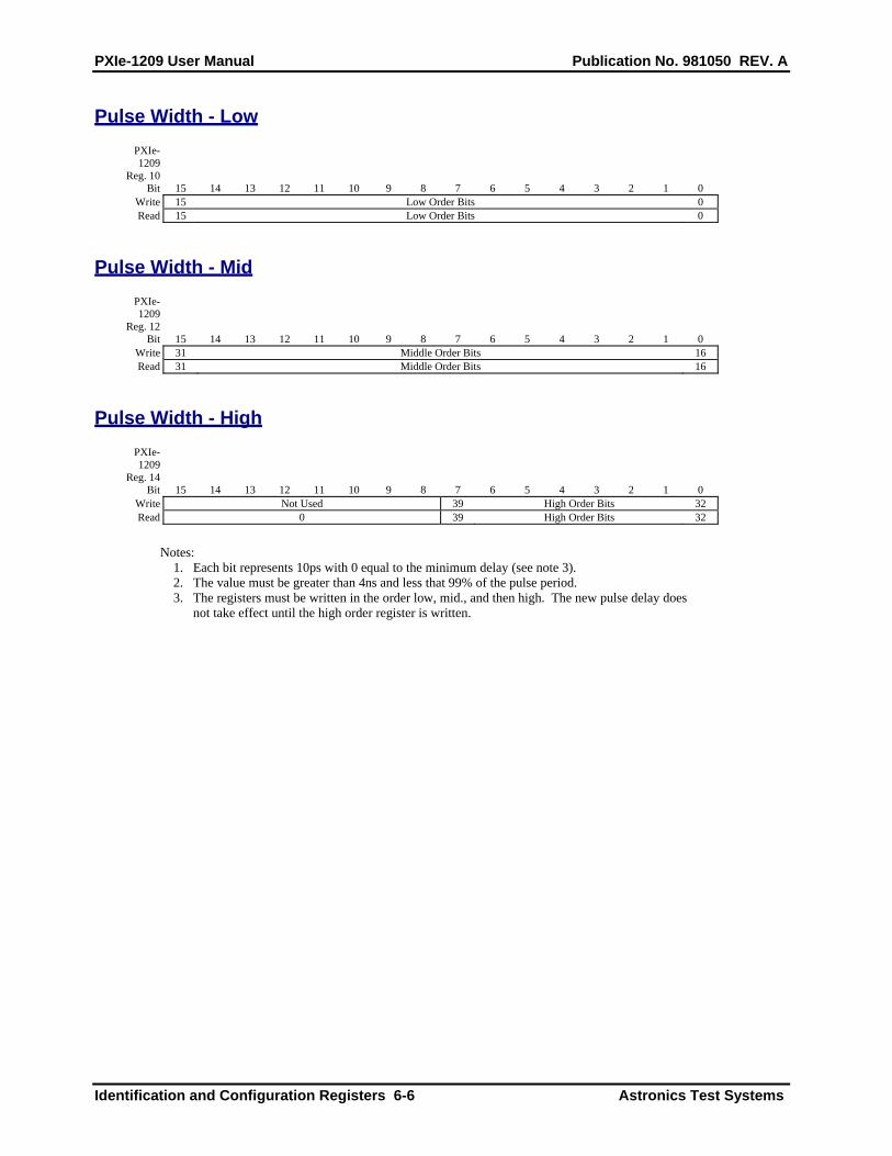
PXIe-1209 User Manual Publication No. 981050 REV. A
Identification and Configuration Registers 6-6 Astronics Test Systems
Pulse Width - Low
PXIe-1209
Reg. 10
Bit 15 14 13 12 11 10 9 8 7 6 5 4 3 2 1 0 Write 15 Low Order Bits 0 Read 15 Low Order Bits 0
Pulse Width - Mid
PXIe-1209
Reg. 12
Bit 15 14 13 12 11 10 9 8 7 6 5 4 3 2 1 0 Write 31 Middle Order Bits 16 Read 31 Middle Order Bits 16
Pulse Width - High
PXIe-1209
Reg. 14
Bit 15 14 13 12 11 10 9 8 7 6 5 4 3 2 1 0 Write Not Used 39 High Order Bits 32 Read 0 39 High Order Bits 32
Notes: 1. Each bit represents 10ps with 0 equal to the minimum delay (see note 3). 2. The value must be greater than 4ns and less that 99% of the pulse period. 3. The registers must be written in the order low, mid., and then high. The new pulse delay does
not take effect until the high order register is written.
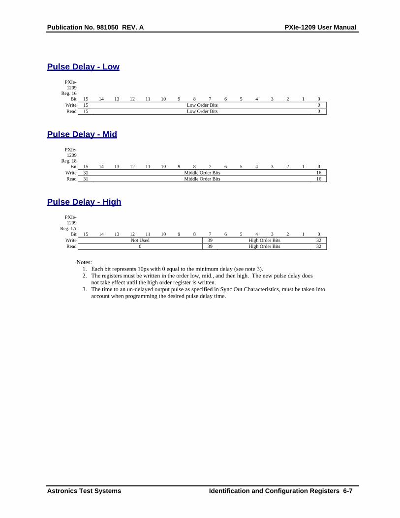
Publication No. 981050 REV. A PXIe-1209 User Manual
Astronics Test Systems Identification and Configuration Registers 6-7
Pulse Delay - Low
PXIe-1209
Reg. 16
Bit 15 14 13 12 11 10 9 8 7 6 5 4 3 2 1 0 Write 15 Low Order Bits 0 Read 15 Low Order Bits 0
Pulse Delay - Mid
PXIe-1209
Reg. 18
Bit 15 14 13 12 11 10 9 8 7 6 5 4 3 2 1 0 Write 31 Middle Order Bits 16 Read 31 Middle Order Bits 16
Pulse Delay - High
PXIe-1209
Reg. 1A
Bit 15 14 13 12 11 10 9 8 7 6 5 4 3 2 1 0 Write Not Used 39 High Order Bits 32 Read 0 39 High Order Bits 32
Notes: 1. Each bit represents 10ps with 0 equal to the minimum delay (see note 3). 2. The registers must be written in the order low, mid., and then high. The new pulse delay does
not take effect until the high order register is written. 3. The time to an un-delayed output pulse as specified in Sync Out Characteristics, must be taken into
account when programming the desired pulse delay time.
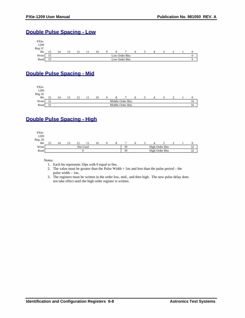
PXIe-1209 User Manual Publication No. 981050 REV. A
Identification and Configuration Registers 6-8 Astronics Test Systems
Double Pulse Spacing - Low
PXIe-1209
Reg.1C
Bit 15 14 13 12 11 10 9 8 7 6 5 4 3 2 1 0 Write 15 Low Order Bits 0 Read 15 Low Order Bits 0
Double Pulse Spacing - Mid
PXIe-1209
Reg.1E
Bit 15 14 13 12 11 10 9 8 7 6 5 4 3 2 1 0 Write 31 Middle Order Bits 16 Read 31 Middle Order Bits 16
Double Pulse Spacing - High
PXIe-1209
Reg. 20
Bit 15 14 13 12 11 10 9 8 7 6 5 4 3 2 1 0 Write Not Used 39 High Order Bits 32 Read 0 39 High Order Bits 32
Notes: 1. Each bit represents 10ps with 0 equal to 0ns. 2. The value must be greater than the Pulse Width + 1ns and less than the pulse period – the
pulse width – 1ns. 3. The registers must be written in the order low, mid., and then high. The new pulse delay does
not take effect until the high order register is written.
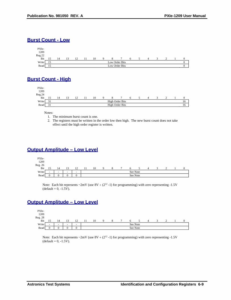
Publication No. 981050 REV. A PXIe-1209 User Manual
Astronics Test Systems Identification and Configuration Registers 6-9
Burst Count - Low
PXIe-1209
Reg.22
Bit 15 14 13 12 11 10 9 8 7 6 5 4 3 2 1 0 Write 15 Low Order Bits 0 Read 15 Low Order Bits 0
Burst Count - High
PXIe-1209
Reg.24
Bit 15 14 13 12 11 10 9 8 7 6 5 4 3 2 1 0 Write 31 High Order Bits 16 Read 31 High Order Bits 16
Notes: 1. The minimum burst count is one. 2. The registers must be written in the order low then high. The new burst count does not take
effect until the high order register is written.
Output Amplitude – Low Level
PXIe-1209
Reg. 26
Bit 15 14 13 12 11 10 9 8 7 6 5 4 3 2 1 0 Write - - - - See Note Read 0 0 0 0 See Note
Note: Each bit represents ~2mV (use 8V (212 -1) for programming) with zero representing -1.5V (default = 0, -1.5V).
Output Amplitude – Low Level
PXIe-1209
Reg. 28
Bit 15 14 13 12 11 10 9 8 7 6 5 4 3 2 1 0 Write - - - - See Note Read 0 0 0 0 See Note
Note: Each bit represents ~2mV (use 8V (212 -1) for programming) with zero representing -1.5V (default = 0, -1.5V).
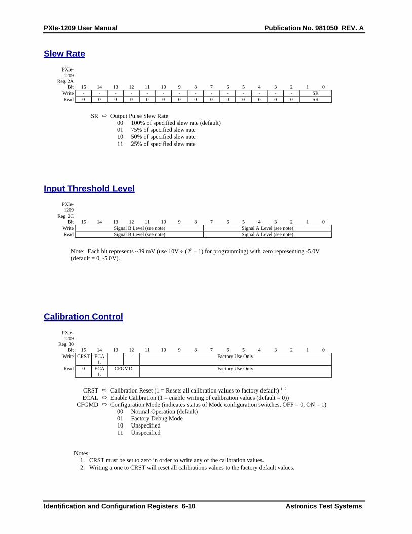
PXIe-1209 User Manual Publication No. 981050 REV. A
Identification and Configuration Registers 6-10 Astronics Test Systems
Slew Rate
PXIe-1209
Reg. 2A
Bit 15 14 13 12 11 10 9 8 7 6 5 4 3 2 1 0 Write - - - - - - - - - - - - - - SR Read 0 0 0 0 0 0 0 0 0 0 0 0 0 0 SR
SR Output Pulse Slew Rate
00 100% of specified slew rate (default) 01 75% of specified slew rate 10 50% of specified slew rate 11 25% of specified slew rate
Input Threshold Level
PXIe-1209
Reg. 2C
Bit 15 14 13 12 11 10 9 8 7 6 5 4 3 2 1 0 Write Signal B Level (see note) Signal A Level (see note) Read Signal B Level (see note) Signal A Level (see note)
Note: Each bit represents ~39 mV (use 10V (28 – 1) for programming) with zero representing -5.0V (default = 0, -5.0V).
Calibration Control
PXIe-1209
Reg. 30
Bit 15 14 13 12 11 10 9 8 7 6 5 4 3 2 1 0 Write CRST ECA
L - - Factory Use Only
Read 0 ECAL
CFGMD Factory Use Only
CRST Calibration Reset (1 = Resets all calibration values to factory default) 1, 2 ECAL Enable Calibration (1 = enable writing of calibration values (default = 0)) CFGMD Configuration Mode (indicates status of Mode configuration switches, OFF = 0, ON = 1)
00 Normal Operation (default) 01 Factory Debug Mode 10 Unspecified 11 Unspecified
Notes: 1. CRST must be set to zero in order to write any of the calibration values. 2. Writing a one to CRST will reset all calibrations values to the factory default values.

Publication No. 981050 REV. A PXIe-1209 User Manual
Astronics Test Systems Identification and Configuration Registers 6-11
Reference Count - Low
PXIe-1209
Reg.78
Bit 15 14 13 12 11 10 9 8 7 6 5 4 3 2 1 0 Write 15 (read only) 0 Read 15 Low Order Bits 0
Reference Count - High
PXIe-1209
Reg.7A
Bit 15 14 13 12 11 10 9 8 7 6 5 4 3 2 1 0 Write 31 (read only) 16 Read 31 High Order Bits 16
Notes: 1. The count is a 2’s complement integer value. Each count represents a difference of approximately
0.0025ppm. A positive value indicates that the internal VCXO is slower than the external reference. 2. The registers must be read in the order low then high.

PXIe-1209 User Manual Publication No. 981050 REV. A
Identification and Configuration Registers 6-12 Astronics Test Systems
This page was left intentionally blank.