Embed Size (px)
Citation preview

CALIBRATION PROCEDURE
PXIe-5673Vector Signal Generator
This document contains the verification procedures for the PXIe-5673 Vector Signal Generator. Refer to ni.com/calibration for more information about calibration solutions.
ContentsSoftware.................................................................................................................................... 2Documentation.......................................................................................................................... 2Calibration Interval................................................................................................................... 2Test Equipment......................................................................................................................... 3Test Conditions......................................................................................................................... 4Initial Setup............................................................................................................................... 5Test System Characterization ................................................................................................... 5
Characterizing the Power Splitter..................................................................................... 5As-Found and As-Left Limits................................................................................................... 8Verification............................................................................................................................... 8
Verifying LO Output Power Accuracy............................................................................. 9Verifying Modulation Impairments.................................................................................. 9Verifying Modulation Bandwidth and Impairments ........................................................ 11Verifying Output Power Level Accuracy......................................................................... 14Verifying Output Intermodulation Products..................................................................... 18Verifying Noise Floor....................................................................................................... 20Verifying RF Harmonics .................................................................................................. 22Verifying Baseband Linearity-Related Spurs................................................................... 23Verifying Single Sideband Phase Noise at 10 kHz Offset ............................................... 25Verifying Frequency Accuracy ........................................................................................ 26
Adjustment................................................................................................................................ 27Reverification ........................................................................................................................... 27Updating Calibration Date........................................................................................................ 28Worldwide Support and Services ............................................................................................. 28

2 | ni.com | PXIe-5673 Calibration Procedure
SoftwareTo calibrate the PXIe-5673, you must install NI-RFSG version 1.8 or later on the calibration system. You can download the latest version of NI-RFSG at ni.com/updates.
NI-RFSG supports programming the calibration procedures in LabVIEW. Refer to Table 1 for file locations.
DocumentationYou might find the following documentation helpful as you write the calibration procedure:
• PXIe-5673 Specifications• NI RF Signal Generators Getting Started Guide• NI RF Signal Generators Help, including LabVIEW programming references
The latest versions of these documents are available on ni.com/manuals.
This calibration procedure calibrates the PXIe-5673 as a single device. To calibrate the PXIe-5450 Waveform Generator, PXIe-5611 IQ Modulator, or PXI-5650/5651/5652 RF Analog Signal Generator individually, refer to their calibration procedures at ni.com/manuals.
Calibration IntervalThe measurement accuracy requirements of your application determine how often you should calibrate your device. NI recommends that you perform a complete calibration for the PXIe-5673 at least once a year. You can shorten this calibration interval based on the accuracy demands of your application.
Table 1. Calibration File Locations
File Name and Location Description
<IVI>\Bin\niRFSG.dll NI-RFSG driver containing the entire NI-RFSG API, including calibration functions.
<LabVIEW >\instr.lib\niRFSG\niRFSG.llb
LabVIEW VI library containing VIs for calling the NI-RFSG calibration API. You can access calibration VIs from the NI-RFSG Calibration section of the LabVIEW Functions palette.

PXIe-5673 Calibration Procedure | © National Instruments | 3
Test EquipmentTable 2 lists the equipment NI recommends for the performance verification procedures. If the recommended equipment is not available, select a substitute using the minimum requirements listed in the table.
Table 2. Recommended Equipment for PXIe-5673 Calibration
EquipmentRecommended
Model Where UsedMinimum
Requirements
Spectrum analyzer Rohde & Schwarz (R&S) FSU Spectrum Analyzer with high-frequency preamplifier option (B23)
Modulation impairments,Modulation bandwidth and impairments,Output power level accuracy,Output intermodulation products,Noise floor,RF harmonics,Baseband linearity-related spurs,Single-sideband phase noise,Frequency accuracy
Frequency range: 50 MHz to 19.8 GHzNoise floor: <-152 dBm/Hz to 6.6 GHz
SMA(m)-to-SMA(m) cable, 36 inches
Huber+Suhner (H+S) ST-18-SMAm/SMAm/36
Operating frequency: DC to 18 GHzImpedance: 50 ΩInsertion loss: <1.5 dBReturn loss: >19 dBConnectors: SMA(m)
BNC(m)-to-BNC(m) cable, 36 inches
— 50 Ω, RG-233
Frequency reference Symmetricom/Datum8040 Rubidium Frequency Standard
Modulation impairments,Modulation bandwidth and impairments,Output power level accuracy,Output intermodulation products,Noise floor,RF harmonics,Baseband linearity-related spurs,Single-sideband phase noise
Frequency: 10 MHzFrequency accuracy: ±1E-9
BNC(m)-to-SMA(m) cable, 36 inches
— 50 Ω, RG-233
Power meter Anritsu ML2438A and an MA2472 diode sensor
LO output power,Output power level accuracy
Frequency range: 50 MHz to 6.6 GHzPower range: -70 dBm to +10 dBmAccuracy: 0.5%
SMA(m)-to-N(f) adapter
S.M. Electronics SM4241
VSWR: 1.15:1

4 | ni.com | PXIe-5673 Calibration Procedure
Test ConditionsThe following setup and environmental conditions are required to ensure the PXIe-5673 meets published specifications.
• Verify that the PXIe-5611, PXIe-5450, and PXI-5650/5651/5652 are properly connected as indicated in the NI RF Signal Generators Getting Started Guide before starting verification.
• Keep cabling as short as possible. Long cables and wires act as antennas, picking up extra noise that can affect measurements.
• Verify that all connections, including front panel connections and screws, are secure.
• Use a torque wrench appropriate for the type of RF connector you are using. NI recommends using a 0.565 N · m (5 lb · in.) torque wrench for SMA connectors and a 0.90 N · m (8 lb · in.) torque wrench for 3.5 mm connectors.
Power splitter Aeroflex/Weinschel 1593
Output power level accuracy
VSWR: 1.25:1Amplitude tracking: <0.25 dB
6 dB attenuator Anritsu 41KB-6 Frequency range: DC to 12 GHzVSWR: 1.1:1
SMA(m)-to-SMA(m) adapter
(H+S) 32_N-SMA-50-1/11_NE
VSWR: 1.05:1
50 Ω terminator (included in the PXIe-5673 kit)
NI 778353-01 — —
PXIe-5673 cable accessory kit (Matched-length I/Q semi-rigid SMA cables (4x)LO semi-rigid SMA cable (1)RF flexible SMA cable (1x))
NI 780567-01 — —
SMA torque wrench (1 N · m)
NI 187106-01 — —
Table 2. Recommended Equipment for PXIe-5673 Calibration (Continued)
EquipmentRecommended
Model Where UsedMinimum
Requirements

PXIe-5673 Calibration Procedure | © National Instruments | 5
• Ensure that the PXI/PXI Express chassis fan speed is set to HIGH, that the fan filters, if present, are clean, and that the empty slots contain filler panels. For more information, refer to the Maintain Forced-Air Cooling Note to Users document available at ni.com/manuals.
• Keep relative humidity between 10% and 90%, noncondensing.
• Maintain an ambient temperature of 23 °C ± 5 °C.
• Allow a warm-up time of at least 30 minutes after the chassis is powered on. The warm-up time ensures that the PXIe-5611 is at a stable operating temperature.
• Perform a self-calibration on the PXIe-5450 Waveform Generator.
• In each verification procedure, insert a delay between configuring all devices and acquiring the measurement. This delay may need to be adjusted depending on the instruments used but should always be at least 1,000 ms for the first iteration, 1,000 ms when the power level changes, and 100 ms for each other iteration.
• Zero and calibrate the power meter sensors before each test.
Initial SetupRefer to the NI RF Signal Generators Getting Started Guide for information about how to install the software and hardware and how to configure the device in MAX.
Test System CharacterizationUse the following procedures to characterize the test system response. Use the results of these procedures in the Verification section of this document.
Characterizing the Power SplitterSeveral procedures in this document require using a splitter that has been characterized to remove error from future measurements. Complete the following steps to characterize a splitter using an PXI-5650/5651/5652, power meter, and spectrum analyzer, as shown in Figure 1.
1. Disconnect the PXIe-5611 LO IN front panel connector from the PXI-5650/5651/5652 RF OUT front panel connector.
2. Connect the power meter power sensor to the PXI-5650/5651/5652 RF OUT front panel connector.
3. Generate a tone with the PXI-5650/5651/5652 with the following niRFSG property settings:
• Frequency (Hz): 85 MHz
• Power Level (dBm): -10 dBm
4. Use the power meter to measure the output power.

6 | ni.com | PXIe-5673 Calibration Procedure
5. Repeat steps 3 through 4 for the following frequency ranges in 5 MHz increments, including endpoints:
• PXI-5650: 85 MHz to 1.3 GHz
• PXI-5651: 85 MHz to 3.3 GHz
• PXI-5652: 85 MHz to 6.6 GHz
Store the resulting measurements as direct [i] (dB).
6. Disconnect the power sensor from the PXI-5650/5651/5652 RF OUT front panel connector.
7. Connect the input port of the power splitter to the PXI-5650/5651/5652 RF OUT front panel connector through the SMA(m)-to-SMA(m) adapter.
Note If you use a cable, it should be as short as possible. The cable should always be used with the splitter for subsequent verification procedures in this document that require a splitter.
8. Connect one available output port of the power splitter to the power sensor without a cable, if possible. Label this port A.
Note Remember the port to which the power sensor is connected. The power sensor must be connected to the same port for subsequent procedures in this document.
9. Connect the other output port of the power splitter to a 6 dB attenuator. Label this port B.
10. Connect the other port of the 6 dB attenuator to the spectrum analyzer RF INPUT front panel connector through the SMA(m)-to-SMA(m) cable as shown in Figure 1.

PXIe-5673 Calibration Procedure | © National Instruments | 7
11. Configure the reference level of the spectrum analyzer to -30 dBm. The spectrum analyzer is used only for termination.
Figure 1. Splitter Characterization Setup
12. Repeat steps 3 through 4 for the following frequency ranges in 5 MHz increments, including endpoints:
• PXI-5650: 85 MHz to 1.3 GHz
• PXI-5651: 85 MHz to 3.3 GHz
• PXI-5652: 85 MHz to 6.6 GHz
Store the resulting measurements as splitter [i] (dB).
1 PXI-5650/5651/5652 RF Analog Signal Generator(PXI-5652 shown)
2 Splitter3 Power Sensor4 N(f)-to-SMA(m) Adapter5 Power Meter
6 CH A Connector7 Spectrum Analyzer8 SMA(m)-to-SMA(m) Cable9 RF INPUT Connector10 6 dB Attenuator11 SMA(m)-to-SMA(m) Adapter
5
6
9
7
10
1 2
11
4
3
8
8 | ni.com | PXIe-5673 Calibration Procedure
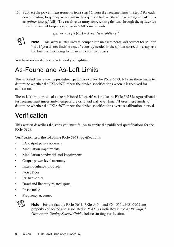
13. Subtract the power measurements from step 12 from the measurements in step 5 for each corresponding frequency, as shown in the equation below. Store the resulting calculations as splitter loss [i] (dB). The result is an array representing the loss through the splitter for the entire needed frequency range in 5 MHz increments.
splitter loss [i] (dB) = direct [i] - splitter [i]
Note This array is later used to compensate measurements and correct for splitter loss. If you do not find the exact frequency needed in the splitter correction array, use the loss corresponding to the next closest frequency.
You have successfully characterized your splitter.
As-Found and As-Left LimitsThe as-found limits are the published specifications for the PXIe-5673. NI uses these limits to determine whether the PXIe-5673 meets the device specifications when it is received for calibration.
The as-left limits are equal to the published NI specifications for the PXIe-5673 less guard bands for measurement uncertainty, temperature drift, and drift over time. NI uses these limits to determine whether the PXIe-5673 meets the device specifications over its calibration interval.
VerificationThis section describes the steps you must follow to verify the published specifications for the PXIe-5673.
Verification tests the following PXIe-5673 specifications:
• LO output power accuracy
• Modulation impairments
• Modulation bandwidth and impairments
• Output power level accuracy
• Intermodulation products
• Noise floor
• RF harmonics
• Baseband linearity-related spurs
• Phase noise
• Frequency accuracy
Note Ensure that the PXIe-5611, PXIe-5450, and PXI-5650/5651/5652 are properly connected and associated in MAX, as indicated in the NI RF Signal Generators Getting Started Guide, before starting verification.
PXIe-5673 Calibration Procedure | © National Instruments | 9
Verification of the PXIe-5673 is complete only after you have successfully completed all tests in this section.
Verifying LO Output Power AccuracyComplete the following steps to verify the LO output power accuracy of the PXIe-5673 module using a power meter.
1. Connect the PXIe-5611 LO OUT front panel connector to the power meter through the SMA(m)-to-N(f) adapter.
2. Generate a signal with the following niRFSG property settings:
• Frequency (Hz): 85 MHz
• Power Level (dBm): 0 dBm
• Generation Mode: CW
• LO OUT Enabled: Enabled
3. Use the power meter to measure the LO OUT power.
4. Compare the measured LO OUT output power to the limit in Table 3.
5. Repeat steps 2 through 4 for the following frequency ranges in 10 MHz increments, including endpoints:
• PXI-5650: 85 MHz to 1.3 GHz
• PXI-5651: 85 MHz to 3.3 GHz
• PXI-5652: 85 MHz to 6.6 GHz
Store the resulting measurements.
If the results are within the selected test limit, the device has passed this portion of the verification.
Verifying Modulation ImpairmentsComplete the following steps to verify the modulation impairments of the PXIe-5673 using a spectrum analyzer.
1. Connect the PXIe-5611 RF OUT front panel connector to the spectrum analyzer RF INPUT front panel connector through the SMA(m)-to-SMA(m) cable.
2. Connect the PXIe-5450 CLK IN front panel connector to any rubidium frequency reference rear panel BNC connector through the BNC(m)-to-SMA(m) cable.
3. Connect the PXIe-5450 CLK OUT front panel connector to the PXI-5650/5651/5652 REF IN/OUT front panel connector.
Table 3. LO Output Power Accuracy Verification Upper Test Limits
LO Output Power (dBm) LO Output Power Test Limit (dB)
0 ±1.0
Note: This specification is unwarranted.

10 | ni.com | PXIe-5673 Calibration Procedure
4. Connect any available rubidium frequency reference rear panel BNC connector to the spectrum analyzer REF IN rear panel connector through the BNC(m)-to-BNC(m) cable.
5. Generate a single-sideband tone with a +1 MHz offset from the carrier signal with the following niRFSG property settings:
• Frequency (Hz): 85 MHz
• Power Level (dBm): 0 dBm
• Generation Mode: Arb Waveform
• Reference Clock Source: ClkIn
The image appears at 84 MHz, and the carrier leakage appears at 85 MHz.
6. Use the spectrum analyzer to measure the mean power of the RF output using the following spectrum analyzer parameter settings:
• Center frequency: (Frequency in step 5) + 1 MHz
• Reference level: +5 dBm
• Frequency span: 0 Hz
• Resolution bandwidth: 500 Hz
• Sweep time: 5 ms
• Reference clock source: External
Note Zero-span mode of the spectrum analyzer shortens test time by avoiding unnecessary frequency sweeping. To obtain the average power, convert the zero-span trace data to linear volts, perform a mean calculation, and then convert the linear volts back to dBm.
7. Use the spectrum analyzer to measure the mean power of the image using the following spectrum analyzer parameter settings:
• Center frequency: (Frequency in step 5) -1 MHz
• Reference level: +5 dBm
• Frequency span: 0 Hz
• Resolution bandwidth: 500 Hz
• Sweep time: 5 ms
• Reference clock source: External
8. Use the spectrum analyzer to measure the mean power of the carrier using the following spectrum analyzer parameter settings:
• Center frequency: Equivalent to the frequency in step 5
• Reference level: +5 dBm
• Frequency span: 0 Hz
• Resolution bandwidth: 500 Hz
• Sweep time: 5 ms
• Reference clock source: External
PXIe-5673 Calibration Procedure | © National Instruments | 11
9. Calculate the image suppression ratio (ISR) and carrier suppression ratio (CSR) according to the following formulas and save the values:
ISR = Measured Image Power - Measured RF Output Power
CSR = Measured Carrier Leakage Power - Measured RF Output Power
10. Repeat steps 5 though 9 for the following LO frequency ranges in 10 MHz steps, including endpoints:
• PXI-5650: 85 MHz to 1.3 GHz
• PXI-5651: 85 MHz to 3.3 GHz
• PXI-5652: 85 MHz to 6.6 GHz
Store the resulting measurements.
Note With the baseband set to 1 MHz and a 0 dBm single-sideband tone, the RF output is always 1 MHz above the LO frequency, the image is 1 MHz below the LO frequency, and the carrier leakage is at the LO frequency.
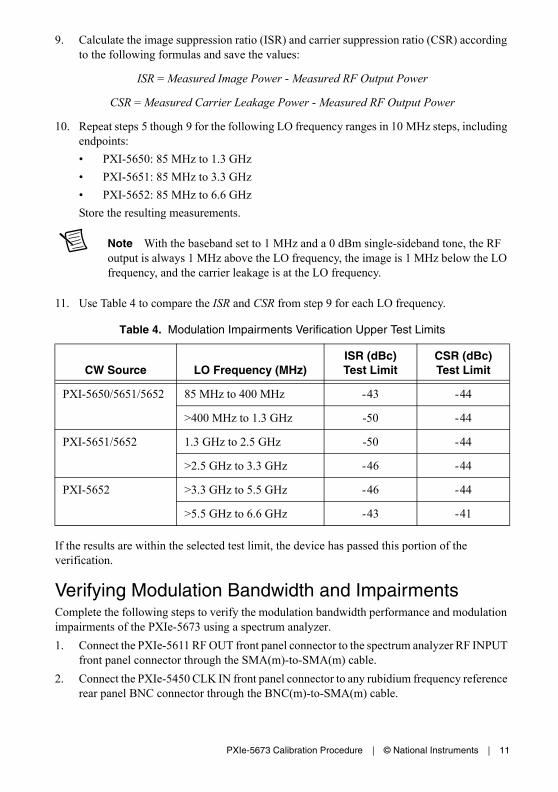
11. Use Table 4 to compare the ISR and CSR from step 9 for each LO frequency.
If the results are within the selected test limit, the device has passed this portion of the verification.
Verifying Modulation Bandwidth and ImpairmentsComplete the following steps to verify the modulation bandwidth performance and modulation impairments of the PXIe-5673 using a spectrum analyzer.
1. Connect the PXIe-5611 RF OUT front panel connector to the spectrum analyzer RF INPUT front panel connector through the SMA(m)-to-SMA(m) cable.
2. Connect the PXIe-5450 CLK IN front panel connector to any rubidium frequency reference rear panel BNC connector through the BNC(m)-to-SMA(m) cable.
Table 4. Modulation Impairments Verification Upper Test Limits
CW Source LO Frequency (MHz)ISR (dBc)Test Limit
CSR (dBc) Test Limit
PXI-5650/5651/5652 85 MHz to 400 MHz -43 -44
>400 MHz to 1.3 GHz -50 -44
PXI-5651/5652 1.3 GHz to 2.5 GHz -50 -44
>2.5 GHz to 3.3 GHz -46 -44
PXI-5652 >3.3 GHz to 5.5 GHz -46 -44
>5.5 GHz to 6.6 GHz -43 -41

12 | ni.com | PXIe-5673 Calibration Procedure
3. Connect the PXIe-5450 CLK OUT front panel connector to the PXI-5650/5651/5652 REF IN/OUT front panel connector.
4. Connect any available rubidium frequency reference rear panel BNC connector to the spectrum analyzer REF IN rear panel connector through the BNC(m)-to-BNC(m) cable.
5. Generate an I/Q tone at -50 MHz offset from the carrier with the following niRFSG property settings:
• Frequency (Hz): 200 MHz
• Power Level (dBm): 0 dBm
• Generation Mode: Arb Waveform
• Reference Clock Source: ClkIn
6. Use the spectrum analyzer to measure the mean output power of the RF output using the following spectrum analyzer parameter settings:
• Center frequency: (Frequency in step 5) + (offset in step 5)
• Reference level: +5 dBm
• Frequency span: 0 Hz
• Resolution bandwidth: 500 Hz
• Sweep time: 5 ms
• Reference clock source: External
7. Use the spectrum analyzer to measure the mean output power of image using the following spectrum analyzer parameter settings:
• Center frequency: (Frequency in step 5) - (offset in step 5)
• Reference level: +5 dBm
• Frequency span: 0 Hz
• Resolution bandwidth: 500 Hz
• Sweep time: 5 ms
• Reference clock source: External
8. Calculate the ISR according to the following formula and save the values:
ISR = Measured Image Power - Measured RF Output Power
9. Repeat steps 5 through 8 for every offset frequency from -50 MHz to +50 MHz in 5 MHz increments while keeping the LO frequency fixed.
Tip Set the niRFSG Generation Mode property to CW to generate a 0 Hz offset. The ISR with a 0 Hz frequency offset cannot be measured, and the 0 Hz data point can be ignored.
10. Calculate the relative modulation bandwidth flatness by subtracting the RF output power measured at 0 Hz offset from the RF output powers measured at each of the other offset frequencies.
PXIe-5673 Calibration Procedure | © National Instruments | 13
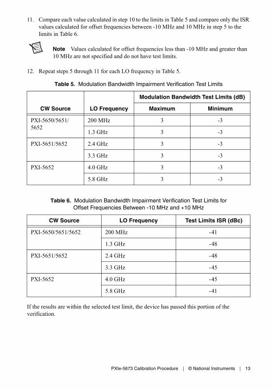
11. Compare each value calculated in step 10 to the limits in Table 5 and compare only the ISR values calculated for offset frequencies between -10 MHz and 10 MHz in step 5 to the limits in Table 6.
Note Values calculated for offset frequencies less than -10 MHz and greater than 10 MHz are not specified and do not have test limits.
12. Repeat steps 5 through 11 for each LO frequency in Table 5.
If the results are within the selected test limit, the device has passed this portion of the verification.
Table 5. Modulation Bandwidth Impairment Verification Test Limits
CW Source LO Frequency
Modulation Bandwidth Test Limits (dB)
Maximum Minimum
PXI-5650/5651/5652
200 MHz 3 -3
1.3 GHz 3 -3
PXI-5651/5652 2.4 GHz 3 -3
3.3 GHz 3 -3
PXI-5652 4.0 GHz 3 -3
5.8 GHz 3 -3
Table 6. Modulation Bandwidth Impairment Verification Test Limits forOffset Frequencies Between -10 MHz and +10 MHz
CW Source LO Frequency Test Limits ISR (dBc)
PXI-5650/5651/5652 200 MHz -41
1.3 GHz -48
PXI-5651/5652 2.4 GHz -48
3.3 GHz -45
PXI-5652 4.0 GHz -45
5.8 GHz -41

14 | ni.com | PXIe-5673 Calibration Procedure
Verifying Output Power Level AccuracyComplete the following steps to verify the output power level accuracy of the PXIe-5673 using a power meter, rubidium frequency standard, spectrum analyzer, power splitter, and 6 dB attenuator.
Figure 2. Connecting Hardware to Verify Output Power Level Accuracy
1 PXIe-5450 Waveform Generator2 PXIe-5611 IQ Modulator3 PXI-5650/5651/5652 RF Analog Signal Generator
(PXI-5652 shown)4 BNC(m)-to-SMA(m) Cable5 Power Sensor6 Rubidium Frequency Source Rear Panel7 BNC(m)-to-BNC(m) Cable Power Meter8 CH A Connector9 Connection from Rubidium Frequency Source to Spectrum
Analyzer REF IN Rear Panel Connector
10 RF INPUT Connector11 Spectrum Analyzer12 SMA(m)-to-SMA(m) Cable13 6 dB Attenuator14 SMA(m)-to-SMA(m) Adapter15 Power Splitter16 N(f)-to-SMA(m) Adapter17 Power Meter
J100 J200J101
1 2 3
5
17
8
6
10
119
7
12
13
15
14
16
4

PXIe-5673 Calibration Procedure | © National Instruments | 15
Note The attenuator is placed in front of the spectrum analyzer to improve the spectrum analyzer return loss. The power splitter must be characterized so that you can account for its loss. Refer to the Characterizing the Power Splitter section for more information about how to characterize your power splitter.
1. Connect the input port of the power splitter to the PXIe-5611 RF OUT front panel connector through the SMA(m)-to-SMA(m) adapter.
2. Connect the PXIe-5450 CLK IN front panel connector to any rubidium frequency reference rear panel BNC connector through the BNC(m)-to-SMA(m) cable.
3. Connect the PXIe-5450 CLK OUT front panel connector to the PXI-5650/5651/5652 REF IN/OUT front panel connector.
4. Connect any available rubidium frequency reference rear panel BNC connector to the spectrum analyzer REF IN rear panel connector through the BNC(m)-to-BNC(m) cable.
Note The port used to connect the power splitter to the power sensor in step 8 of the Characterizing the Power Splitter section must be the same port used to connect the power splitter to the power meter in step 5 of this section.
5. Connect port A of the power splitter to the power meter through the SMA(m)-to-N(f) adapter.
Note The port used to connect the power splitter to the 6 dB attenuator in step 9 of the Characterizing the Power Splitter section must be the same port used to connect the power splitter to the 6 dB attenuator in step 6 of this section.
6. Connect port B of the power splitter to the 6 dB attenuator.
7. Connect the available port of the 6 dB attenuator to the spectrum analyzer RF INPUT front panel connector through the SMA(m)-to-SMA(m) cable.
8. Generate a single-sideband tone with a +1 MHz offset from the carrier with the following niRFSG property settings:
• Frequency (Hz): 85 MHz
• Power Level (dBm): 5 dBm
• Generation Mode: Arb Waveform
• Reference Clock Source: ClkIn
9. Use the power meter to measure power splitter-compensated output power.
Note Measurements must be adjusted to account for the splitter loss stored in the Characterizing the Power Splitter section, as shown in the following equation.
Measurement = power meter reading [i] + splitter loss [i]
16 | ni.com | PXIe-5673 Calibration Procedure
10. Repeat steps 8 through 9 for the following frequency ranges in 20 MHz increments, including endpoints:
• PXI-5650: 85 MHz to 1.3 GHz
• PXI-5651: 85 MHz to 3.3 GHz
• PXI-5652: 85 MHz to 6.6 GHz
Store the resulting measurements.
11. Set the niRFSG Power Level property to 0 dBm, and repeat steps 8 through 10.
12. Set the niRFSG Power Level property to -30 dBm, and repeat steps 8 through 10, measuring the power using both the power meter and spectrum analyzer. Use the following parameter settings for the spectrum analyzer:
• Center frequency: (Frequency in step 8) + 1 MHz
• Reference level: -30 dBm
• Frequency span: 0 Hz
• Resolution bandwidth: 500 Hz
• Sweep time: 20 ms
• Reference clock source: External
• Attenuation: 5 dB
• Preamplifier: niRFSG Power Level property
13. Use the power meter measurements to calculate a correction for the spectrum analyzer inaccuracies and attenuator loss with the following equation:
Corrections [i] = Power Meter [i] - SpecAn [i]
Note The SpecAn [i] values in the above equation are used only to determine the Corrections [i] values that are used in the -60 dBm and -90 dBm measurements described in steps 14 and 15. When verifying the -30 dBm measurements, you need to use only the Power Meter [i] values.
14. Set the niRFSG Power Level property to -60 dBm, and repeat steps 8 through 10 using only the spectrum analyzer and its measured correction to measure the power accuracy using the following spectrum analyzer parameter settings:
• Center frequency: (Frequency in step 8) + 1 MHz
• Reference level: -30 dBm
• Frequency span: 0 Hz
• Resolution bandwidth: 500 Hz
• Sweep time: 20 ms
• Reference clock source: External
• Attenuation: 5 dB
• Preamplifier: On

PXIe-5673 Calibration Procedure | © National Instruments | 17
Note To maintain the same measurement uncertainty as the power meter, you must apply the corrections found in step 15 to the measured results as shown in the following equation:
AdjustedMeasurement [i] = SpecAn [i] + Corrections [i] + Splitter Loss [i]15. Set the niRFSG Power Level property to -90 dBm and repeat steps 8 through 10 using only
the spectrum analyzer and its measured correction to measure the power accuracy using the following spectrum analyzer parameter settings:
• Center frequency: (Frequency in step 8) + 1 MHz
• Reference level: -30 dBm
• Frequency span: 0 Hz
• Resolution bandwidth: 500 Hz
• Sweep time: 200 ms
• Reference clock source: External
• Attenuation: 5 dB
• Preamplifier: On
16. Measure tone power with the spectrum analyzer and calculate the adjusted tone power using the AdjustedMeasurement [i] equation from step 14.
17. Compare the measured values from steps 8 through 15 to the corresponding limits in Table 7.
If the results are within the selected test limit, the device has passed this portion of the verification.
Table 7. Output Power Level Accuracy Verification Test Limits
Output Power (dBm) As-Found Limit (dB) As-Left Limit (dB)
5 ±0.75 ±0.55
0 ±0.75 ±0.55
-10 ±0.75 ±0.55
-30 ±0.75 ±0.55
-60 ±0.75 ±0.55
-90 ±0.75 ±0.55

18 | ni.com | PXIe-5673 Calibration Procedure
Verifying Output Intermodulation ProductsComplete the following steps to verify the output intermodulation (IMD) performance of an PXIe-5673 using a spectrum analyzer. Complete this test for each iteration in Table 8.
1. Connect the PXIe-5611 RF OUT front panel connector to the spectrum analyzer RF INPUT front panel connector through the SMA(m)-to-SMA(m) cable.
2. Connect the PXIe-5450 CLK IN front panel connector to any rubidium frequency reference rear panel BNC connector through the BNC(m)-to-SMA(m) cable.
3. Connect the PXIe-5450 CLK OUT front panel connector to the PXI-5650/5651/5652 REF IN/OUT front panel connector.
4. Connect any available rubidium frequency reference rear panel BNC connector to the spectrum analyzer REF IN rear panel connector through the BNC(m)-BNC(m) cable.
5. Generate two single-sideband tones simultaneously at 2 MHz (F1) offset from the carrier and 2.3 MHz (F2) offset from the carrier with the following niRFSG property settings:
• Frequency (Hz): 85 MHz
• Power Level (dBm): 0 dBm
• Generation Mode: Arb Waveform
• Power Level Type: Peak Power
• Reference Clock Source: ClkIn
The power of each tone should be approximately -6 dBm.
6. Set the output power for the given measurements in Table 8.
7. Use the spectrum analyzer to measure the mean amplitude of the first fundamental tone. Name this value P1. For example, when the LO is set to 85 MHz, measure the first fundamental signal power at 87 MHz (LO + F1). Use the following spectrum analyzer parameter settings:
• Center frequency: (Frequency in step 5) + F1
• Reference level: 0 dBm
• Frequency span: 0 Hz
• Resolution bandwidth: 500 Hz
• Sweep time: 5 ms
• Reference clock source: External
8. Use the spectrum analyzer to measure the mean amplitude of the second fundamental tone. Name this value P2. For example, when the LO is set to 85 MHz, measure the second fundamental signal powers at 87.3 MHz (LO + F2). Use the following spectrum analyzer parameter settings:
• Center frequency: (Frequency in step 5) + F2
• Reference level: 0 dBm
• Frequency span: 0 Hz

PXIe-5673 Calibration Procedure | © National Instruments | 19
• Resolution bandwidth: 500 Hz
• Sweep time: 5 ms
• Reference clock source: External
9. Use the spectrum analyzer to measure the mean amplitude of the first close-in IMD tone at 86.7 MHz (LO + 2F1 - F2). Name this value I1. Use the following spectrum analyzer parameter settings:
• Center frequency: (Frequency in step 5) + F1
• Reference level: 0 dBm
• Frequency span: 0 Hz
• Resolution bandwidth: 500 Hz
• Sweep time: 5 ms
• Reference clock source: External
10. Use the spectrum analyzer to measure the mean amplitude of the second close-in IMD tone at 87.6 MHz (LO + 2F2 - F1). Name this value I2. Use the following spectrum analyzer parameter settings:
• Center frequency: (Frequency in step 5) + F2
• Reference level: 0 dBm
• Frequency span: 0 Hz
• Resolution bandwidth: 500 Hz
• Sweep time: 5 ms
• Reference clock source: External
11. Calculate output IMD using the following equation:
Output IMD = Large IMD tone power (I1 or I2) - Small fundamental tone power (P1 or P2)
12. Compare the Output IMD value from step 11 to the corresponding limit in Table 8.
13. Repeat steps 5 through 12 for the following frequency ranges in 250 MHz increments, including endpoints:
• PXI-5650: 85 MHz to 1.3 GHz
• PXI-5651: 85 MHz to 3.3 GHz
• PXI-5652: 85 MHz to 6.6 GHz
Store the resulting measurements.
20 | ni.com | PXIe-5673 Calibration Procedure
14. Repeat steps 5 through 12 with a power level of -30 dBm and a spectrum analyzer reference level of -30 dBm.
Verifying Noise FloorComplete the following steps to verify the noise floor performance of an PXIe-5673 module using a spectrum analyzer.
1. Connect the PXIe-5611 RF OUT front panel connector to the spectrum analyzer RF INPUT front panel connector through the SMA(m)-to-SMA(m) cable.
2. Connect the PXIe-5450 CLK IN front panel connector to any rubidium frequency reference rear panel BNC connector through the BNC(m)-to-SMA(m) cable.
3. Connect the PXIe-5450 CLK OUT front panel connector to the PXI-5650/5651/5652 REF IN/OUT front panel connector.
4. Connect any available rubidium frequency reference rear panel BNC connector to the spectrum analyzer REF IN rear panel connector through the BNC(m)-to-BNC(m) cable.
5. Generate an arbitrary waveform signal using an array of all zeros with the following niRFSG property settings:
• Frequency (Hz): 85 MHz
• Power Level (dBm): +10 dBm
• Generation Mode: Arb Waveform
Table 8. Intermodulation Products Verification Test Limits with -6 dBm per Tone
CW Source LO Frequencies R3 Upper Limits (dBc)
PXI-5650/5651/5652 85 MHz to 250 MHz -45
>250 MHz to 1.3 GHz -48
PXI-5651/5652 >1.3 GHz to 3.3 GHz -45
PXI-5652 >3.3 GHz to 6.6 GHz -40
Table 9. Intermodulation Products Verification Test Limits with -36 dBm per Tone
CW Source LO Frequencies R3 Upper Limits (dBc)
PXI-5650/5651/5652 85 MHz to 250 MHz -45
>250 MHz to 1.3 GHz -50
PXI-5651/5652 >1.3 GHz to 3.3 GHz -48
PXI-5652 >3.3 GHz to 6.6 GHz -46

PXIe-5673 Calibration Procedure | © National Instruments | 21
• Power Level Type: Peak Power
• Reference Clock Source: ClkIn
6. Measure the output noise floor 2 MHz above the generated frequency using the spectrum analyzer. Minimize the spectrum analyzer noise contribution by using the preamplifier, minimal attenuation, and a low reference level. Use the following spectrum analyzer parameter settings:
• Center frequency: (Frequency in step 5) + 2 MHz
• Reference level: -50 dBm
• Frequency span: 0 Hz
• Resolution bandwidth: 100 kHz
• Sweep time: 5 ms
• Reference clock source: External
• Attenuation: 5 dB
• Preamplifier: On
7. Repeat steps 5 through 6 for the following LO frequency ranges in 250 MHz increments, including endpoints:
• PXI-5650: 85 MHz to 1.3 GHz
• PXI-5651: 85 MHz to 3.3 GHz
• PXI-5652: 85 MHz to 6.6 GHz
Store the resulting measurements.
8. Compare the measured values to the corresponding limits in Table 10.
9. Repeat steps 5 through 8 for the remaining output power values listed in Table 10.
If the results are within the selected test limit, the device has passed this portion of the verification.
Table 10. Noise Floor Upper Test Limits
Output Power (dBm)
PXI-5650/5651/5652 PXI-5651/5652 PXI-5652
LO Frequencies85 MHz to 250 MHz
LO Frequencies>250 MHz to
1.3 GHz
LO Frequencies>1.3 GHz to
3.3 GHz
LO Frequencies>3.3 GHz to
6.6 GHz
+10 -133 dBm/Hz -134 dBm/Hz -134 dBm/Hz -134 dBm/Hz
0 -140 dBm/Hz -141 dBm/Hz -141 dBm/Hz -141 dBm/Hz
-10 -145 dBm/Hz -145 dBm/Hz -145 dBm/Hz -145 dBm/Hz
-30 -152 dBm/Hz -152 dBm/Hz -152 dBm/Hz -152 dBm/Hz
22 | ni.com | PXIe-5673 Calibration Procedure
Verifying RF HarmonicsComplete the following steps to verify the harmonic performance of an PXIe-5673 module using a spectrum analyzer.
1. Connect the PXIe-5611 RF OUT front panel connector to the spectrum analyzer RF INPUT front panel connector through the SMA(m)-to-SMA(m) cable.
2. Connect the PXIe-5450 CLK IN front panel connector to any rubidium frequency reference rear panel BNC connector through the BNC(m)-to-SMA(m) cable.
3. Connect the PXIe-5450 CLK OUT front panel connector to the PXI-5650/5651/5652 REF IN/OUT front panel connector.
4. Connect any available rubidium frequency reference rear panel BNC connector to the spectrum analyzer REF IN rear panel connector through the BNC(m)-to-BNC(m) cable.
5. Generate a signal with the following niRFSG property settings:
• Frequency (Hz): 100 MHz
• Power Level (dBm): 0 dBm
• Generation Mode: CW
• Reference Clock Source: ClkIn
6. Use the spectrum analyzer to measure the fundamental tone power using the following spectrum analyzer parameter settings (name this measurement F):
• Center frequency: Frequency from step 5
• Reference level: +5 dBm
• Frequency span: 0 Hz
• Resolution bandwidth: 500 Hz
• Sweep time: 5 ms
• Reference clock source: External
7. Use the spectrum analyzer to measure each harmonic tone listed in Table 11 using the following spectrum analyzer settings (name this measurement Hx, where x is the harmonic number):
• Center frequency: (Frequency from step 5) × (harmonic number)
• Reference level: +5 dBm
• Frequency span: 0 Hz
• Resolution bandwidth: 500 Hz
• Sweep time: 5 ms
• Reference clock source: External
Note Only measure subharmonic tones at fundamental frequencies ≥3.3 GHz.

PXIe-5673 Calibration Procedure | © National Instruments | 23
8. Calculate the power level in dBc of each harmonic tone ≤6.6 GHz by subtracting the fundamental power from step 6 from the harmonic power from step 7, as shown in the following equation:
Pharmonic = Hx - F9. Compare the values calculated in step 8 to the corresponding limits in Table 11.
10. Repeat steps 6 through 9 for the following frequency ranges:
• PXI-5650: 100 MHz to 500 MHz in 10 MHz increments, including endpoints and 500 MHz to 1.3 GHz in 50 MHz increments, including endpoints
• PXI-5651: 100 MHz to 500 MHz in 10 MHz increments, including endpoints and 500 MHz to 3.3 GHz in 50 MHz increments, including endpoints
• PXI-5652: 100 MHz to 500 MHz in 10 MHz increments, including endpoints, and 500 MHz to 6.6 GHz in 50 MHz increments, including endpoints
Note Harmonic, subharmonic, and non-integer harmonic levels outside the device frequency range are typical.
If the results are within the selected test limit, the device has passed this portion of the verification.
Verifying Baseband Linearity-Related SpursComplete the following steps to verify the baseband-related spur levels of the PXIe-5673 using a spectrum analyzer.
1. Connect the PXIe-5611 RF OUT front panel connector to the spectrum analyzer RF INPUT front panel connector through the SMA(m)-to-SMA(m) cable.
2. Connect the PXIe-5450 CLK IN front panel connector to any rubidium frequency reference rear panel BNC connector through the BNC(m)-to-SMA(m) cable.
Table 11. RF Harmonic Power Upper Test Limits
Harmo-nic
PXIe-5650/5651/5652
PXIe-5651/5652 PXIe-5652
100 MHz to
250 MHz>250 MHz to 1.3 GHz
>1.3 GHz to
2.2 GHz
>2.2 GHz to
3.3 GHz
>3.3 GHz to
3.5 GHz
>3.5 GHz to
4.4 GHz
>4.4 GHz to
6.6 GHz
2nd (2F)
-23.0 dBc -28.0 dBc -23.0 dBc
-23.0 dBc
— — —
3rd (3F)
-23.0 dBc -28.0 dBc -23.0 dBc
— — — —
Half (0.5F)
— — — — -34.0 dBc
-34.0 dBc
-34.0 dBc
1.5 (1.5F)
— — — — -41.0 dBc
-46.0 dBc
—

24 | ni.com | PXIe-5673 Calibration Procedure
3. Connect the PXIe-5450 CLK OUT front panel connector to the PXI-5650/5651/5652 REF IN/OUT front panel connector.
4. Connect any available rubidium frequency reference rear panel BNC connector to the spectrum analyzer REF IN rear panel connector through the BNC(m)-to-BNC(m) cable.
5. Generate a single-sideband tone with a +1 MHz offset from the carrier signal with the following niRFSG property settings:
• Frequency (Hz): 85 MHz
• Power Level (dBm): 0 dBm
• Generation Mode: Arb Waveform
• Reference Clock Source: ClkIn
6. Use the spectrum analyzer to measure the mean RF output using the following spectrum analyzer parameter settings (name this measurement RF):
• Center frequency: (Frequency in step 5) + 1 MHz
• Reference level: +5 dBm
• Frequency span: 0 Hz
• Resolution bandwidth: 500 Hz
• Sweep time: 5 ms
• Reference clock source: External
7. Use the spectrum analyzer to measure the baseband linearity-related spur using the following spectrum analyzer parameter settings (name this measurement B):
• Center frequency: (Frequency in step 5) - 3 MHz
• Reference level: +5 dBm
• Frequency span: 0 Hz
• Resolution bandwidth: 500 Hz
• Sweep time: 5 ms
• Reference clock source: External
8. Calculate the power level of the baseband linearity-related spur in dBc by subtracting the measured RF output power from step 6 from the measured baseband linearity-related spur from step 7, as shown in the following equation:
Pbaseband = B - RF9. Compare the value calculated in step 8 to the corresponding limits in Table 12.
10. Repeat steps 5 through 9 for the following frequency ranges in 200 MHz increments, including endpoints:
• PXI-5650: 85 MHz to 1.3 GHz
• PXI-5651: 85 MHz to 3.3 GHz
• PXI-5652: 85 MHz to 6.6 GHz
Store the resulting measurements.
PXIe-5673 Calibration Procedure | © National Instruments | 25
If the results are within the selected limit, the device has passed this portion of the verification.
Verifying Single Sideband Phase Noise at 10 kHz OffsetComplete the following steps to verify the single sideband (SSB) phase noise of the PXIe-5673 using a spectrum analyzer.
1. Connect the PXIe-5611 RF OUT front panel connector to the spectrum analyzer RF INPUT front panel connector through the SMA(m)-to-SMA(m) cable.
2. Connect the PXIe-5450 CLK IN front panel connector to any rubidium frequency reference rear panel BNC connector through the BNC(m)-to-SMA(m) cable.
3. Connect the PXIe-5450 CLK OUT front panel connector to the PXI-5650/5651/5652 REF IN/OUT front panel connector.
4. Connect any available rubidium frequency reference rear panel BNC connector to the spectrum analyzer REF IN rear panel connector through the BNC(m)-to-BNC(m) cable.
5. Generate a single-sideband tone with a +3 MHz offset from the carrier signal with the following niRFSG property settings:
• Frequency (Hz): 1 GHz
• Power Level (dBm): 0 dBm
• Generation Mode: Arb Waveform
• Reference Clock Source: ClkIn
6. Use the spectrum analyzer to measure the maximum power within the configured span of the spectrum analyzer using the following spectrum analyzer parameter settings and record the value:
• Center frequency: (Frequency in step 5) + 3 MHz
• Reference level: 0 dBm
• Frequency span: 100 Hz
• Resolution bandwidth: 10 Hz
• Reference clock source: External
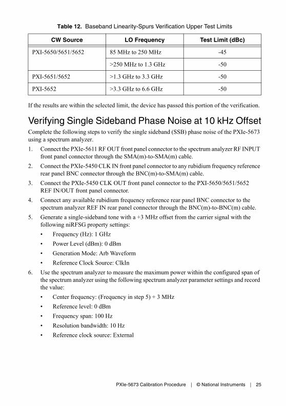
Table 12. Baseband Linearity-Spurs Verification Upper Test Limits
CW Source LO Frequency Test Limit (dBc)
PXI-5650/5651/5652 85 MHz to 250 MHz -45
>250 MHz to 1.3 GHz -50
PXI-5651/5652 >1.3 GHz to 3.3 GHz -50
PXI-5652 >3.3 GHz to 6.6 GHz -50

26 | ni.com | PXIe-5673 Calibration Procedure
7. Use the spectrum analyzer to measure the mean power within the configured span of the spectrum analyzer using the following spectrum analyzer parameter settings and record the value:
• Center frequency: (Frequency in step 6) + 10 kHz
• Reference level: 0 dBm
• Frequency span: 100 Hz
• Resolution bandwidth: 10 Hz
• Reference clock source: External
• Trace averaging: 20 traces
8. Apply the following equation to the value measured in step 7:
phase noiseSSB at 10 kHz offset = Measurement - 10log (RBW)
9. Subtract the measurement recorded in step 6 from the value calculated in step 8.
10. Verify that the value calculated in step 9 meets the limits as specified in Table 13.
11. Repeat steps 6 through 10 for the remaining frequencies listed in the Frequency column in Table 13.
If the results are within the selected test limit, the device has passed this portion of the verification.
Verifying Frequency AccuracyComplete the following steps to verify the frequency accuracy of an PXIe-5673 using a spectrum analyzer.
1. Connect the PXIe-5611 RF OUT front panel connector to the spectrum analyzer RF INPUT front panel connector through the SMA(m)-to-SMA(m) cable.
2. Connect any available rubidium frequency reference rear panel BNC connector to the spectrum analyzer REF IN rear panel connector through the BNC(m)-to-SMA(m) cable.
Table 13. SSB Phase Noise at 10 kHz Offset
CW Source Frequency (GHz) Test Limit (dBc/Hz)
PXI-5650/5651/5652 0.5 <-111
1.0 <-105
PXI-5651/5652 2.0 <-98
3.0 <-95
PXI-5652 4.0 <-93
5.0 <-90
6.6 <-90

PXIe-5673 Calibration Procedure | © National Instruments | 27
3. Connect the PXIe-5450 CLK IN front panel connector to the PXI-5650/5651/5652 REF IN/OUT front panel connector.
4. Generate a signal with the following niRFSG properties:
• Frequency (Hz): 400 MHz
• Power Level (dBm): 0 dBm
• Generation Mode: CW
• Reference Clock Source: Onboard Clock
5. Use the spectrum analyzer to measure the frequency of the peak tone using the following spectrum analyzer parameter settings:
• Center frequency: 400 MHz
• Reference level: +5 dBm
• Resolution bandwidth: 100 Hz
• Span: 100 kHz
• Reference clock source: External
• Frequency counter resolution: 1 Hz
6. Verify that the measurement in step 5 is within the 9 ppm test limit, with respect to 400 MHz.
If the results are within the selected test limit, the device has passed this portion of the verification.
AdjustmentTo adjust the PXIe-5673 to meet published specifications, you must adjust the modules that comprise the PXIe-5673 system. To calibrate the PXI-5650/5651/5652, PXIe-5450, and PXIe-5611 modules individually, refer to their calibration procedures at ni.com/manuals.
ReverificationRepeat the Verification section to determine the as-left status of the device.
Note If any test fails reverification after performing an adjustment, verify that you have met the Test Conditions before returning your device to NI. Refer to Worldwide Support and Services for information about support resources or service requests.
© 2009–2017 National Instruments. All rights reserved.
372857E-01 Jun17
Refer to the NI Trademarks and Logo Guidelines at ni.com/trademarks for more information on NI trademarks. Other product and company names mentioned herein are trademarks or trade names of their respective companies. For patents covering NI products/technology, refer to the appropriate location: Help»Patents in your software, the patents.txt file on your media, or the National Instruments Patents Notice at ni.com/patents. You can find information about end-user license agreements (EULAs) and third-party legal notices in the readme file for your NI product. Refer to the Export Compliance Information at ni.com/legal/export-compliance for the NI global trade compliance policy and how to obtain relevant HTS codes, ECCNs, and other import/export data. NI MAKES NO EXPRESS OR IMPLIED WARRANTIES AS TO THE ACCURACY OF THE INFORMATION CONTAINED HEREIN AND SHALL NOT BE LIABLE FOR ANY ERRORS. U.S. Government Customers: The data contained in this manual was developed at private expense and is subject to the applicable limited rights and restricted data rights as set forth in FAR 52.227-14, DFAR 252.227-7014, and DFAR 252.227-7015.
Updating Calibration DatePerforming any adjustment procedure on the PXIe-5611 updates the calibration date.
If you do not want to perform an adjustment, you can update the calibration date without making any adjustments by initializing an external calibration and closing the external calibration.
1. Call the niRFSG Initialize External Calibration VI.
2. Call the niRFSG Close External Calibration VI to close the session. Set the write calibration to hardware? parameter to TRUE to store the results to the EEPROM on the PXIe-5673.
Worldwide Support and ServicesThe NI website is your complete resource for technical support. At ni.com/support you have access to everything from troubleshooting and application development self-help resources to email and phone assistance from NI Application Engineers.
Visit ni.com/services for NI Factory Installation Services, repairs, extended warranty, and other services.
Visit ni.com/register to register your NI product. Product registration facilitates technical support and ensures that you receive important information updates from NI.
A Declaration of Conformity (DoC) is our claim of compliance with the Council of the European Communities using the manufacturer’s declaration of conformity. This system affords the user protection for electromagnetic compatibility (EMC) and product safety. You can obtain the DoC for your product by visiting ni.com/certification. If your product supports calibration, you can obtain the calibration certificate for your product at ni.com/calibration.
NI corporate headquarters is located at 11500 North Mopac Expressway, Austin, Texas, 78759-3504. NI also has offices located around the world. For telephone support in the United States, create your service request at ni.com/support or dial 1 866 ASK MYNI (275 6964). For telephone support outside the United States, visit the Worldwide Offices section of ni.com/niglobal to access the branch office websites, which provide up-to-date contact information, support phone numbers, email addresses, and current events.