Embed Size (px)
Citation preview

MELSEC Q Series
Programmable Logic Controller
User's Manual(Functioning and Programming)
QCPU (Q Mode)
INDUSTRIAL AUTOMATIONMITSUBISHI ELECTRIC EUROPE B.V.Art. no.: 130022
2000 03 16SH 080038-A


A - 1
• SAFETY INSTRUCTIONS • (Always read these instructions before using this equipment.)
When using Mitsubishi equipment, thoroughly read this manual and the associated manuals introduced in
this manual. Also pay careful attention to safety and handle the module properly.
These SAFETY PRECAUTIONS classify the safety precautions into two categories: "DANGER" and
"CAUTION".
! DANGER
CAUTION!
Indicates that incorrect handling may cause hazardous conditions,resulting in death or severe injury.
Indicates that incorrect handling may cause hazardous conditions, resulting in medium or slight personal injury or physical damage.
Note that the ! CAUTION level may lead to a serious consequence according to the circumstances.
Always follow the instructions of both levels because they are important to personal safety.
Please save this manual to make it accessible when required and always forward it to the end user.
[Design Precautions]
! DANGER
• Install a safety circuit external to the PLC that keeps the entire system safe even when there are
problems with the external power supply or the PLC module. Otherwise, trouble could result
from erroneous output or erroneous operation.
(1) Outside the PLC, construct mechanical damage preventing interlock circuits such as
emergency stop, protective circuits, positioning upper and lower limits switches and
interlocking forward/reverse operations.
(2) When the PLC detects the following problems, it will stop calculation and turn off all output in
the case of (a). In the case of (b), it will stop calculation and hold or turn off all output
according to the parameter setting.
(a) The power supply module has over current protection equipment and over voltage
protection equipment.
(b) The PLC CPUs self-diagnostic functions, such as the watchdog timer error, detect
problems.
In addition, all output will be turned on when there are problems that the PLC CPU cannot
detect, such as in the I/O controller. Build a fail safe circuit exterior to the PLC that will make
sure the equipment operates safely at such times. Refer to " LOADING AND
INSTALLATION" in QCPU (Q Mode) User's Manual (Hardware Design/Maintenance and
Inspection) for example fail safe circuits.
(3) Output could be left on or off when there is trouble in the outputs module relay or transistor.
So build an external monitoring circuit that will monitor any single outputs that could cause
serious trouble.

A - 2
[Design Precautions]
! DANGER
• When overcurrent which exceeds the rating or caused by short-circuited load flows in the output
module for a long time, it may cause smoke or fire. To prevent this, configure an external safety
circuit, such as fuse.
• Build a circuit that turns on the external power supply when the PLC main module power is
turned on. If the external power supply is turned on first, it could result in erroneous output or
erroneous operation.
• When there are communication problems with the data link, refer to the corresponding data link
manual for the operating status of each station.
Not doing so could result in erroneous output or erroneous operation.
• When connecting a peripheral device to the CPU module or connecting a personal computer or
the like to the intelligent function module to exercise control (data change) on the running PLC,
configure up an interlock circuit in the sequence program to ensure that the whole system will
always operate safely.
Also before exercising other control (program change, operating status change (status control))
on the running PLC, read the manual carefully and fully confirm safety.
Especially for the above control on the remote PLC from an external device, an immediate
action may not be taken for PLC trouble due to a data communication fault.
In addition to configuring up the interlock circuit in the sequence program, corrective and other
actions to be taken as a system for the occurrence of a data communication fault should be
predetermined between the external device and PLC CPU.
! CAUTION
• Do not bunch the control wires or communication cables with the main circuit or power wires, or
install them close to each other. They should be installed 100 mm (3.94 inch) or more from each
other.
Not doing so could result in noise that would cause erroneous operation.
• When controlling items like lamp load, heater or solenoid valve using an output module, large
current (approximately ten times greater than that present in normal circumstances) may flow
when the output is turned OFF to ON.
Take measures such as replacing the module with one having sufficient rated current.

A - 3
[Installation Precautions]
! CAUTION
• Use the PLC in an environment that meets the general specifications contained in this manual.
Using this PLC in an environment outside the range of the general specifications could result in
electric shock, fire, erroneous operation, and damage to or deterioration of the product.
• Hold down the module loading lever at the module bottom, and securely insert the module fixing
hook into the fixing hole in the base module. Incorrect loading of the module can cause a
malfunction, failure or drop.
When using the PLC in the environment of much vibration, tighten the module with a screw.
Tighten the screw in the specified torque range.
Undertightening can cause a drop, short circuit or malfunction.
Overtightening can cause a drop, short circuit or malfunction due to damage to the screw or
module.
• When installing more cables, be sure that the base module and the module connectors are
installed correctly.
After installation, check them for looseness.
Poor connections could cause an input or output failure.
• Securely load the memory card into the memory card loading connector.
After loading, check for lifting.
Lifting can cause a malfunction due to a contact fault.
• Completely turn off the external power supply before loading or unloading the module.
Not doing so could result in electric shock or damage to the product.
• Do not directly touch the module's conductive parts or electronic components.
Touching the conductive parts could cause an operation failure or give damage to the module.
[Wiring Precautions]
! DANGER
• Completely turn off the external power supply when installing or placing wiring.
Not completely turning off all power could result in electric shock or damage to the product.
• When turning on the power supply or operating the module after installation or wiring work, be
sure that the module's terminal covers are correctly attached.
Not attaching the terminal cover could result in electric shock.

A - 4
[Wiring Precautions]
! CAUTION
• Be sure to ground the FG terminals and LG terminals to the protective ground conductor. Not
doing so could result in electric shock or erroneous operation.
• When wiring in the PLC, be sure that it is done correctly by checking the product's rated voltage
and the terminal layout.
Connecting a power supply that is different from the rating or incorrectly wiring the product could
result in fire or damage.
• External connections shall be crimped or pressure welded with the specified tools, or correctly
soldered.
Imperfect connections could result in short circuit, fires, or erroneous operation.
• Tighten the terminal screws with the specified torque.
If the terminal screws are loose, it could result in short circuits, fire, or erroneous operation.
Tightening the terminal screws too far may cause damages to the screws and/or the module,
resulting in fallout, short circuits, or malfunction.
• Be sure there are no foreign substances such as sawdust or wiring debris inside the module.
Such debris could cause fires, damage, or erroneous operation.
• The module has an ingress prevention label on its top to prevent foreign matter, such as wire
offcuts, from entering the module during wiring.
Do not peel this label during wiring.
Before starting system operation, be sure to peel this label because of heat dissipation.
[Startup and Maintenance precautions]
! DANGER
• Do not touch the terminals while power is on.
Doing so could cause shock or erroneous operation.
• Correctly connect the battery. Also, do not charge, disassemble, heat, place in fire, short circuit,
or solder the battery.
Mishandling of battery can cause overheating or cracks which could result in injury and fires.
• Switch all phases of the external power supply off when cleaning the module or retightening the
terminal or module mounting screws. Not doing so could result in electric shock.
Undertightening of terminal screws can cause a short circuit or malfunction.
Overtightening of screws can cause damages to the screws and/or the module, resulting in
fallout, short circuits, or malfunction.

A - 5
[Startup and Maintenance precautions]
! CAUTION
• The online operations conducted for the CPU module being operated, connecting the peripheral
device (especially, when changing data or operation status), shall be conducted after the
manual has been carefully read and a sufficient check of safety has been conducted.
Operation mistakes could cause damage or problems with of the module.
• Do not disassemble or modify the modules.
Doing so could cause trouble, erroneous operation, injury, or fire.
• Use a cellular phone or PHS more than 25cm (9.85 inch) away from the PLC.
Not doing so can cause a malfunction.
• Switch all phases of the external power supply off before mounting or removing the module.
If you do not switch off the external power supply, it will cause failure or malfunction of the
module.
[Disposal Precautions]
! CAUTION
• When disposing of this product, treat it as industrial waste.

A - 6
REVISIONS
* The manual number is given on the bottom left of the back cover.
Print Date * Manual Number Revision
Dec., 1999 SH (NA) 080038-A First edition
Japanese Manual Version SH-080020-A
This manual confers no industrial property rights or any rights of any other kind, nor does it confer any patent licenses. Mitsubishi Electric Corporation cannot be held responsible for any problems involving industrial property rights which may occur as a result of using the contents noted in this manual.
1999 MITSUBISHI ELECTRIC CORPORATION

A - 7
INTRODUCTION
Thank you for choosing the Mitsubishi MELSEC-Q Series of General Purpose Programmable Controllers.
Please read this manual carefully so that equipment is used to its optimum.
CONTENTS Safety Instructions..........................................................................................................................................A- 1
Revisions ........................................................................................................................................................A- 6
Contents .........................................................................................................................................................A- 7
About Manuals ...............................................................................................................................................A-15
How to Use This Manuals..............................................................................................................................A-16
About the Generic Terms and Abbreviations................................................................................................A-17
1. OVERVIEW 1- 1 to 1-10
1.1 Features ................................................................................................................................................... 1- 1
1.2 Programs.................................................................................................................................................. 1- 3
1.3 Convenient Programming Devices and Instructions .............................................................................. 1- 6
2. SYSTEM CONFIGURATION 2- 1 to 2- 6
2.1 System Configuration .............................................................................................................................. 2- 1
2.2 System Precaution................................................................................................................................... 2- 4
3. PERFORMANCE SPECIFICATION 3- 1 to 3- 4
4. SEQUENCE PROGRAM CONFIGURATION & EXECUTION CONDITIONS 4- 1 to 4-50
4.1 Sequence Program.................................................................................................................................. 4- 1
4.1.1 Main routine program........................................................................................................................ 4- 3
4.1.2 Sub-routine programs ....................................................................................................................... 4- 4
4.1.3 Interrupt programs............................................................................................................................. 4- 6
4.2 Program Execute Type............................................................................................................................ 4-10
4.2.1 Initial execution type program........................................................................................................... 4-15
4.2.2 Scan execution type program........................................................................................................... 4-17
4.2.3 Low-speed execution type program ................................................................................................. 4-19
4.2.4 Stand-by type program ..................................................................................................................... 4-25
4.2.5 Fixed scan execution type program ................................................................................................. 4-31
4.3 Operation Processing .............................................................................................................................. 4-33
4.3.1 Initial processing................................................................................................................................ 4-33
4.3.2 I/O refresh (I/O module refresh processing) .................................................................................... 4-33
4.3.3 Automatic refresh of the intelligent function module........................................................................ 4-34
4.3.4 END processing ................................................................................................................................ 4-34
4.4 RUN, STOP, PAUSE Operation Processing .......................................................................................... 4-35
4.5 Operation Processing during Momentary Power Failure ....................................................................... 4-36
4.6 Data Clear Processing............................................................................................................................. 4-37

A - 8
4.7 Input/Output Processing & Response Lag.............................................................................................. 4-38
4.7.1 Refresh mode.................................................................................................................................... 4-38
4.7.2 Direct mode....................................................................................................................................... 4-41
4.8 Numeric Values which Can Be Used in Sequence Programs ............................................................... 4-43
4.8.1 BIN (Binary Code) ............................................................................................................................. 4-45
4.8.2 HEX (Hexadecimal) .......................................................................................................................... 4-46
4.8.3 BCD (Binary Coded Decimal)........................................................................................................... 4-47
4.8.4 Real numbers (floating decimal point data) ..................................................................................... 4-48
4.9 Character String Data .............................................................................................................................. 4-50
5. ASSIGNMENT OF I/O NUMBERS 5- 1 to 5-16
5.1 Relationship Between the Number of Stages and Slots of the Expansion Base Unit........................... 5- 1
5.2 Installing Expansion Base Units and Setting the Number of Stages ..................................................... 5- 2
5.3 Base Unit Assignment (Base Mode) ....................................................................................................... 5- 3
5.4 What are I/O Numbers?........................................................................................................................... 5- 6
5.5 Concept of I/O Number Assignment ....................................................................................................... 5- 7
5.6 I/O Assignment by GPPW ....................................................................................................................... 5- 9
5.6.1 Purpose of I/O assignment by GPPW.............................................................................................. 5- 9
5.6.2 Concept of I/O assignment using GPPW......................................................................................... 5-10
5.7 Examples of I/O Number Assignment..................................................................................................... 5-12
5.8 Checking the I/O Numbers ...................................................................................................................... 5-16
6. QCPU FILES 6- 1 to 6-18
6.1 About the QCPU's Memory ..................................................................................................................... 6- 3
6.2 Program Memory ..................................................................................................................................... 6- 6
6.3 About the Standard ROM ........................................................................................................................ 6- 8
6.4 About the Standard RAM......................................................................................................................... 6- 9
6.5 Memory Card ........................................................................................................................................... 6-10
6.6 Writing Data in the Standard ROM or on the Flash Card....................................................................... 6-11
6.7 Executing Standard ROM/Memory Card Programs (Boot Run) ............................................................ 6-13
6.8 Program File Configuration...................................................................................................................... 6-15
6.9 GPPW File Operation and File Handling Precautions............................................................................ 6-16
6.9.1 File operation..................................................................................................................................... 6-16
6.9.2 File handling precautions.................................................................................................................. 6-17
6.9.3 File size ............................................................................................................................................. 6-18
7. FUNCTION 7- 1 to 7-66
7.1 Function List ............................................................................................................................................. 7- 1
7.2 Constant Scan.......................................................................................................................................... 7- 2
7.3 Latch Functions........................................................................................................................................ 7- 5
7.4 Setting the Output (Y) Status when Changing from STOP Status to RUN Status................................ 7- 7
7.5 Clock Function ......................................................................................................................................... 7- 9

A - 9
7.6 Remote Operation.................................................................................................................................... 7-12
7.6.1 Remote RUN/STOP.......................................................................................................................... 7-12
7.6.2 Remote PAUSE ................................................................................................................................ 7-15
7.6.3 Remote RESET................................................................................................................................. 7-17
7.6.4 Remote latch clear ............................................................................................................................ 7-18
7.6.5 Relationship of the remote operation and QCPU RUN/STOP switch............................................. 7-19
7.7 Changing the Response Speed of the QCPU-Compatible Input Module(I/O Response Time) ........... 7-20
7.8 Setting the Switches of the Intelligent-Function Module......................................................................... 7-21
7.9 Monitoring Function ................................................................................................................................. 7-22
7.9.1 Monitor condition setting................................................................................................................... 7-22
7.9.2 Monitoring test for local device ......................................................................................................... 7-26
7.10 Writing in Program during QCPU RUN................................................................................................. 7-28
7.10.1 Writing data in the circuit mode during the RUN status................................................................. 7-28
7.10.2 Writing a batch of files during RUN ................................................................................................ 7-30
7.11 Execution Time Measurement............................................................................................................... 7-32
7.11.1 Program monitor list........................................................................................................................ 7-32
7.11.2 Interrupt program monitor list ......................................................................................................... 7-34
7.11.3 Scan time measurement................................................................................................................. 7-35
7.12 Sampling Trace Function....................................................................................................................... 7-37
7.13 Debug Function with Multiple Users...................................................................................................... 7-46
7.13.1 Multiple-user monitoring function ................................................................................................... 7-47
7.13.2 Multiple-user RUN write function.................................................................................................... 7-48
7.14 Watchdog Timer (WDT)......................................................................................................................... 7-50
7.15 Self-Diagnosis Function......................................................................................................................... 7-52
7.15.1 Interrupt due to error occurrence.................................................................................................... 7-55
7.15.2 LED display when error occurs ...................................................................................................... 7-55
7.15.3 Cancel error..................................................................................................................................... 7-56
7.16 Failure History........................................................................................................................................ 7-57
7.17 System Protect....................................................................................................................................... 7-58
7.18 Password Registration........................................................................................................................... 7-58
7.19 Monitoring QCPU System Status from GPPW (System Monitor)........................................................ 7-60
7.20 LED Display ........................................................................................................................................... 7-62
7.20.1 LED display ..................................................................................................................................... 7-62
7.20.2 Priority setting.................................................................................................................................. 7-64
8. COMMUNICATION WITH INTELLIGENT FUNCTION MODULE/SPECIAL FUNCTION MODULE 8- 1 to 8-10
8.1 Communication Between QCPU and Q-series Intelligent Function Modules ....................................... 8- 1
8.1.1 Initial setting and automatic refresh setting using utility package ................................................... 8- 2
8.1.2 Communication using device initial value ........................................................................................ 8- 3
8.1.3 Communication using FROM/TO instruction ................................................................................... 8- 4
8.1.4 Communication using the intelligent function module device.......................................................... 8- 4
8.1.5 Communication using the instructions dedicated for intelligent function modules ......................... 8- 5
8.2 Request from Intelligent Function Module to QCPU .............................................................................. 8- 6
8.2.1 Interrupt from the intelligent function module................................................................................... 8- 6

A - 10
8.3 Communication Between QCPU and AnS-Series Special Function Modules ...................................... 8- 7
8.3.1 Communication using device initial value ........................................................................................ 8- 7
8.3.2 Communication using FROM/TO instruction ................................................................................... 8- 8
8.3.3 Communication using the intelligent function module device.......................................................... 8- 8
8.3.4 Effects of quicker access to the special function module and countermeasures against them..... 8- 9
9. PARAMETER LIST 9- 1 to 9- 6
10. DEVICES 10- 1 to 10-72
10.1 Device List............................................................................................................................................ 10- 1
10.2 Internal User Devices .......................................................................................................................... 10- 3
10.2.1 Inputs (X) ....................................................................................................................................... 10- 5
10.2.2 Outputs (Y) .................................................................................................................................... 10- 8
10.2.3 Internal relays (M) ......................................................................................................................... 10-10
10.2.4 Latch relays (L) ............................................................................................................................. 10-11
10.2.5 Anunciators (F).............................................................................................................................. 10-12
10.2.6 Edge relay (V) ............................................................................................................................... 10-16
10.2.7 Link relays (B) ............................................................................................................................... 10-17
10.2.8 Special link relays (SB) ................................................................................................................. 10-18
10.2.9 Step relays (S) .............................................................................................................................. 10-18
10.2.10 Timers (T).................................................................................................................................... 10-19
10.2.11 Counters (C)................................................................................................................................ 10-24
10.2.12 Data registers (D)....................................................................................................................... 10-28
10.2.13 Link registers (W)....................................................................................................................... 10-29
10.2.14 Special link registers (SW) ......................................................................................................... 10-30
10.3 Internal System Devices...................................................................................................................... 10-31
10.3.1 Function devices (FX, FY, FD) ..................................................................................................... 10-31
10.3.2 Special relays (SM)....................................................................................................................... 10-33
10.3.3 Special registers (SD)................................................................................................................... 10-34
10.4 Link Direct Devices (J \ )................................................................................................................. 10-35
10.5 Intelligent Function Module Devices (U \G ) .................................................................................. 10-38
10.6 Index Registers (Z) .............................................................................................................................. 10-39
10.6.1 Switching between scan execution type programs and low-speed execution type programs... 10-40
10.6.2 Switching between scan/low-speed execution type programs and interrupt/fixed scan ............ 10-41
execution type programs
10.7 File Registers (R) ................................................................................................................................. 10-43
10.7.1 File register capacity .................................................................................................................... 10-44
10.7.2 Differences in memory card access method by memory card type ............................................ 10-44
10.7.3 Registering the file registers ........................................................................................................ 10-45
10.7.4 File register designation method .................................................................................................. 10-49
10.7.5 Precautions in using file registers................................................................................................. 10-50
10.8 Nesting (N) ........................................................................................................................................... 10-52

A - 11
10.9 Pointers ................................................................................................................................................ 10-53
10.9.1 Local pointers ................................................................................................................................ 10-53
10.9.2 Common pointers.......................................................................................................................... 10-54
10.10 Interrupt Pointers (I) ........................................................................................................................... 10-56
10.11 Other Devices .................................................................................................................................... 10-58
10.11.1 SFC block device (BL) ................................................................................................................ 10-58
10.11.2 SFC transition device (TR) ......................................................................................................... 10-58
10.11.3 Network No. designation device (J) ........................................................................................... 10-58
10.11.4 I/O No. designation device (U) ................................................................................................... 10-59
10.11.5 Macro instruction argument device (VD).................................................................................... 10-60
10.12 Constants ........................................................................................................................................... 10-61
10.12.1 Decimal constants (K)................................................................................................................. 10-61
10.12.2 Hexadecimal constants (H) ........................................................................................................ 10-61
10.12.3 Real numbers (E)........................................................................................................................ 10-62
10.12.4 Character string ( " ).................................................................................................................... 10-62
10.13 Convenient Uses for Devices ............................................................................................................ 10-63
10.13.1 Global devices & local devices................................................................................................... 10-63
10.13.2 Device initial values .................................................................................................................... 10-69
11. QCPU PROCESSING TIME 11- 1 to 11- 4
12. PROCEDURE FOR WRITING PROGRAMS TO QCPU 12- 1 to 12- 8
12.1 Writing Procedure For 1 Program ....................................................................................................... 12- 1
12.1.1 Items to consider when creating one program............................................................................. 12- 1
12.1.2 Procedure for writing programs to the QCPU.............................................................................. 12- 2
12.2 Procedure For Multiple Programs ....................................................................................................... 12- 5
12.2.1 Items to consider when creating multiple programs .................................................................... 12- 5
12.2.2 Procedure for writing programs to the QCPU.............................................................................. 12- 6
APPENDICES App- 1 to App-56
APPENDIX 1 Special Relay List................................................................................................................App- 1
APPENDIX 2 Special Register List ...........................................................................................................App-21
APPENDIX 3 List of Interrupt Pointer Nos. & Interrupt Factors ...............................................................App-55
INDEX Index- 1 to Index- 3

A - 12
(Related manual)................. QCPU (Q Mode) User's Manual (Hardware Design/Maintenance and Inspection)
CONTENTS
1. OVERVIEW
1.1 Overview
1.2 Features
2. SYSTEM CONFIGURATION
2.1 System Configuration
2.2 Precaution on System Configuration
3. GENERAL SPECIFICATIONS
4. HARDWARE SPECIFICATION OF THE CPU MODULE
4.1 Performance Specification
4.2 Part Names and Settings
4.3 Switch Operation After Writing in Program
4.4 Latch Clear Operation
5. POWER SUPPLY MODULE
5.1 Specification
5.1.1 Power supply module specifications
5.1.2 Selecting the power supply module
5.1.3 Precaution when connecting the uninterruptive power supply
5.2 Names of Parts and Settings
6. BASE UNIT AND EXTENSION CABLE
6.1 Base Unit Specification Table
6.2 Extension Cable Specification Table
6.3 The Names of The Parts of The Base Unit
6.4 Setting the Extension Base Unit
6.5 I/O Allocations
7. MEMORY CARD AND BATTERY
7.1 Memory Card Specifications
7.2 Battery Specifications (For CPU Module and SRAM Card)
7.3 Handling the Memory Card
7.4 The Names of The Parts of The Memory Card
7.5 Memory Card Loading/Unloading Procedures
7.6 Installation of Battery (for CPU Module and Memory Card)

A - 13
8. EMC AND LOW-VOLTAGE DIRECTIVES
8.1 Requirements for conformance to EMC Directive
8.1.1 Standards applicable to the EMC Directive
8.1.2 Installation instructions for EMC Directive
8.1.3 Cables
8.1.4 Power supply module
8.1.5 When using Q1AS6 B type base unit
8.1.6 Others
8.2 Requirement to Conform to the Low-Voltage Directive
8.2.1 Standard applied for MELSEC-Q series
8.2.2 MELSEC-Q series PLC selection
8.2.3 Power supply
8.2.4 Control box
8.2.5 Grounding
8.2.6 External wiring
9. LOADING AND INSTALLATION
9.1 General Safety Requirements
9.2 Calculating Heat Generation by PLC
9.3 Module Installation
9.3.1 Precaution on installation
9.3.2 Instructions for mounting the base unit
9.3.3 Installation and removal of module
9.4 Setting the Extension Number of the Extension Base Unit
9.5 Connection and Disconnection of Extension Cable
9.6 Wiring
9.6.1 The precautions on the wiring
9.6.2 Connecting to the power supply module
10. MAINTENANCE AND INSPECTION
10.1 Daily Inspection
10.2 Periodic Inspection
10.3 Battery Replacement
10.3.1 Battery service life
10.3.2 Battery replacement procedure
11. TROUBLESHOOTING
11.1 Troubleshooting Basics
11.2 Troubleshooting
11.2.1 Troubleshooting flowchart
11.2.2 Flowchart for when "MODE" LED is not turned on
11.2.3 Flowchart for when "POWER" LED is turned off
11.2.4 Flowchart for when the "RUN" LED is turned off

A - 14
11.2.5 When the "RUN" LED is flashing
11.2.6 Flowchart for when "ERROR" LED is on/flashing
11.2.7 When "USER" LED is turned on
11.2.8 When "BAT.ARM" LED is turned on
11.2.9 Flowchart for when output load of output module does not turn on
11.2.10 Flowchart for when unable to read a program
11.2.11 Flowchart for when unable to write a program
11.2.12 Flowchart for when it is unable to perform boot operation from memory card
11.2.13 Flowchart for when UNIT VERIFY ERR. occurs
11.2.14 Flowchart for when CONTROL BUS ERR. occurs
11.3 Error Code List
11.3.1 Procedure for reading error codes
11.3.2 Error code list
11.4 Canceling of Errors
11.5 I/O Module Troubleshooting
11.5.1 Input circuit troubleshooting
11.6 Special Relay List
11.7 Special Register List
APPENDICES
APPENDIX 1 Error Code Return to Origin During General Data Processing
APPENDIX 1.1 Error code overall explanation
APPENDIX 1.2 Description of the errors of the error codes (4000H to 4FFFH)
APPENDIX 2 External Dimensions Diagram
APPENDIX 2.1 CPU module
APPENDIX 2.2 Power supply module
APPENDIX 2.3 Main base unit
APPENDIX 2.4 Extension base unit
INDEX
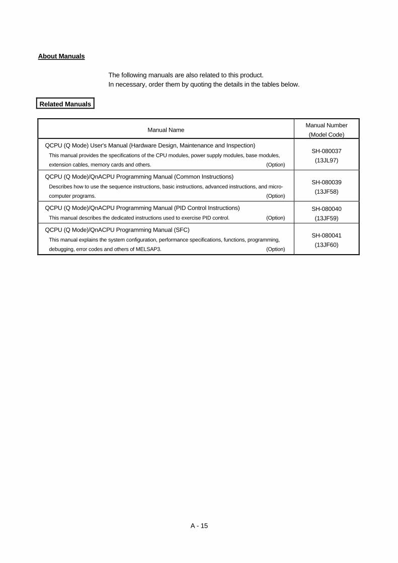
A - 15
About Manuals
The following manuals are also related to this product.
In necessary, order them by quoting the details in the tables below.
Related Manuals
Manual Name Manual Number
(Model Code)
QCPU (Q Mode) User's Manual (Hardware Design, Maintenance and Inspection)
This manual provides the specifications of the CPU modules, power supply modules, base modules,
extension cables, memory cards and others. (Option)
SH-080037
(13JL97)
QCPU (Q Mode)/QnACPU Programming Manual (Common Instructions)
Describes how to use the sequence instructions, basic instructions, advanced instructions, and micro-
computer programs. (Option)
SH-080039
(13JF58)
QCPU (Q Mode)/QnACPU Programming Manual (PID Control Instructions)
This manual describes the dedicated instructions used to exercise PID control. (Option)
SH-080040
(13JF59)
QCPU (Q Mode)/QnACPU Programming Manual (SFC)
This manual explains the system configuration, performance specifications, functions, programming,
debugging, error codes and others of MELSAP3. (Option)
SH-080041
(13JF60)

A - 16
How to Use This Manual
This manual is prepared for users to understand memory map, functions, programs
and devices of the CPU module when you use MELSEC-Q series sequencers.
The manual is classified roughly into three sections as shown below.
(1) Chapters 1 and 2 Describe the outline of the CPU module and the system
configuration. The feature of CPU module and the basics of the
system configuration of CPU are described.
(2) Chapters 3 to 6 Describe the performance specifications, executable program,
I/O No. and memory of the CPU module.
(3) Chapter 7 Describes the functions of the CPU modules.
(4) Chapter 8 Describes communication with intelligent function modules.
(5) Chapters 9 and 10 Describe parameters and devices used in the CPU modules.
(6) Chapter 11 Describes the CPU module processing time.
(7) Chapter 12 Describes the procedure for writing parameters and programs
created at the GPPW to the CPU module.
REMARK
This manual does not explain the functions of power supply modules, base modules,
extension cables, memory cards and batteries of QCPU.
For these functions, refer to the manual shown below.
• QCPU (Q Mode) User's Manual (Hardware Design, Maintenance and Inspection)
A - 17
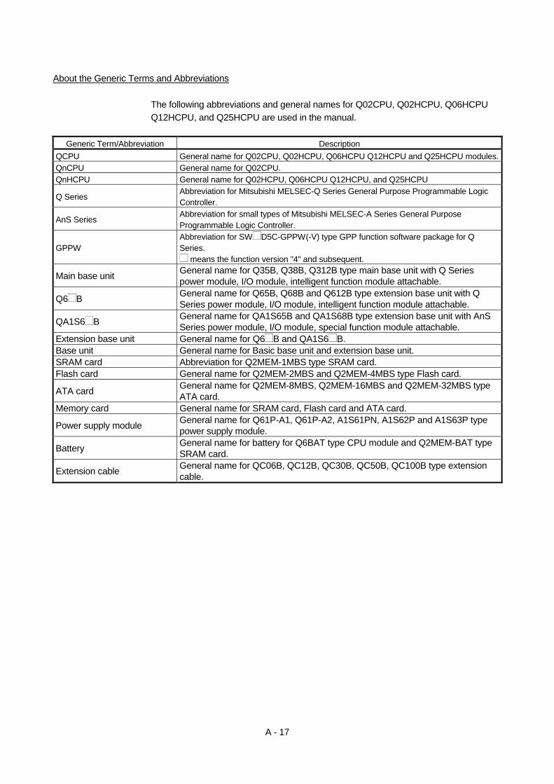
About the Generic Terms and Abbreviations
The following abbreviations and general names for Q02CPU, Q02HCPU, Q06HCPU
Q12HCPU, and Q25HCPU are used in the manual.
Generic Term/Abbreviation Description
QCPU General name for Q02CPU, Q02HCPU, Q06HCPU Q12HCPU and Q25HCPU modules.
QnCPU General name for Q02CPU.
QnHCPU General name for Q02HCPU, Q06HCPU Q12HCPU, and Q25HCPU
Q Series Abbreviation for Mitsubishi MELSEC-Q Series General Purpose Programmable Logic Controller.
AnS Series Abbreviation for small types of Mitsubishi MELSEC-A Series General Purpose Programmable Logic Controller.
GPPW Abbreviation for SW D5C-GPPW(-V) type GPP function software package for Q Series.
means the function version "4" and subsequent.
Main base unit General name for Q35B, Q38B, Q312B type main base unit with Q Series power module, I/O module, intelligent function module attachable.
Q6 B General name for Q65B, Q68B and Q612B type extension base unit with Q Series power module, I/O module, intelligent function module attachable.
QA1S6 B General name for QA1S65B and QA1S68B type extension base unit with AnS Series power module, I/O module, special function module attachable.
Extension base unit General name for Q6 B and QA1S6 B. Base unit General name for Basic base unit and extension base unit. SRAM card Abbreviation for Q2MEM-1MBS type SRAM card. Flash card General name for Q2MEM-2MBS and Q2MEM-4MBS type Flash card.
ATA card General name for Q2MEM-8MBS, Q2MEM-16MBS and Q2MEM-32MBS type ATA card.
Memory card General name for SRAM card, Flash card and ATA card.
Power supply module General name for Q61P-A1, Q61P-A2, A1S61PN, A1S62P and A1S63P type power supply module.
Battery General name for battery for Q6BAT type CPU module and Q2MEM-BAT type SRAM card.
Extension cable General name for QC06B, QC12B, QC30B, QC50B, QC100B type extension cable.

A - 18
MEMO

1 - 1
MELSEC-Q 1. OVERVIEW
1
1. OVERVIEW
This User's Manual describes the memory map, function, program, and device of the
general-purpose sequencers Models Q02CPU, Q02HCPU, Q06HCPU, Q12HCPU and
Q25HCPU (herein after referred to as QCPU. When referred to each module, however,
it is described as Q02CPU,Q02HCPU, Q06HCPU, Q12HCPU, and Q25HCPU.)
Refer to QCPU (Q Mode) User's Manual (Hardware Design/Maintenance and
Inspection) for the specifications of the power module, base unit, extension cable,
memory card, and battery.
1.1 Features
QCPU has the following features:
(1) Controllable multiple I/O points
All QCPUs support 4096 points (X/Y0 to FFF) as the number of actual I/O points
capable of getting access to the I/O module installed on the base unit.
They also support 8192 points max. (X/Y0 to 1FFF) as the number of I/O devices
which can be used in the remote I/O stations such as CC-Link data link and
MELSECNET/MINI-S3 data link.
(2) Lineup according to program capacity
The optimum CPU module for the program capacity to be used can be selected.
Q02CPU, Q02HCPU : 28 k step
Q06HCPI : 60 k step
Q12HCPU : 124 k step
Q25HCPU : 252 k step
(3) Realized high speed processing
Depending on the type of the sequencer, high-speed processing has been
realized. (Example: when LD instruction is used)
Q02CPU :0.079 s
Q02HCPU, Q06HCPU, Q12HCPU, Q25HCPU :0.034 s
In addition, an access to the intelligent function module or an increase in speed
of the link refresh of the network have been realized by the connection system (Q
bus connection) of the newly developed base unit.
Access to the intelligent function module : 20 s /word (approx. 7 times)*1
MELSECNET/10 link refresh processing : 4.6 ms/8k word (approx. 4.3 times)*1
*1: Where Q02HCPU is compared with Q2ASHCPU-S1.

1 - 2
MELSEC-Q 1. OVERVIEW
(4) Increase in debugging efficiency through high-speed communication with
GPPW
In the QCPU, a time required for writing/reading of a program or monitoring has been reduced through the high speed communication at a speed of 115.2 kbps max. by the RS-232, and a communication time efficiency at the time of debugging has been increased. In the Q02HCPU, Q06HCPU, Q12HCPU, and Q25HCPU, a high-speed communication at a speed of 12 Mbps is allowed through the USB. 26 k step program transfer time
0 10 20 30 40 50 60 70 80
Q25HCPU(USB)
Q25HCPU(RS-232)
Q2ASHCPU
A2USHCPU-S1
12
30
86
94
(Unit:sec.)10090 (5) AnS series I/O module or special-function module are available.
For Q series, if an appropriate module is not available, the AnS series I/O module or special-function module can also be used for the QCPU through the use of the QA1S65B/QA1S68B extension base unit.
(6) Saved space by a reduction in size
The installation space for Q series has been reduced by approx. 60 % of the space for AnS series.
0123456789ABCDEF
0123456789ABCDEF
0123456789ABCDEF
0123456789ABCDEF
MELSECQ61P-A1 POWER
MITSUBISHI
PULL
Q25HCPU
MODE RUN ERR
USER BAT
BOOT
USB
PULL
QX10 QX10 QX10 QX10 QX41 QX41 QX41 QX41 QJ71BR11 RUN
T.PASS SD
ERR
MNGD.I.INKRDERR
QJ71BR11 RUN
T.PASS SD
ERR
MNGD.I.INKRDERR
QJ71BR11 RUN
T.PASS SD
ERR
MNGD.I.INKRDERR
QJ71BR11 RUN
T.PASS SD
ERR
MNGD.I.INKRDERR
MITSUBISHI MITSUBISHI
MELSEC A1S62PPOWER
MELSEC A 1 CPUSRUN
ERROR
A1SX101 -2 -3 -4 -5 -6 -7 -
- 8- 9- A- B- C- D- E
1 -2 -3 -4 -5 -6 -7 -
- 8- 9- A- B- C- D - E
A1SY50 A1SX41 A1SY41 A1SX81 A1SY81 A1SX42 A1SY42ERRA B
ERRA B1 -
2 -3 -4 -5 -6 -7 -
- 8- 9- A- B- C- D - E
1 -2 -3 -4 -5 -6 -7 -
- 8- 9- A- B- C- D - E
1 -2 -3 -4 -5 -6 -7 -
- 8- 9- A- B- C- D - E
1 -2 -3 -4 -5 -6 -7 -
- 8- 9- A- B- C- D - E
1 -2 -3 -4 -5 -6 -7 -
- 8- 9- A- B- C- D - E
1 -2 -3 -4 -5 -6 -7 -
- 8- 9- A- B- C- D - E
8 -9 -A -B -C -D -E -
- 1- 2- 3- 4- 5- 6 - 7
A B8 -9 -A -B -C -D -E -
- 1- 2- 3- 4- 5- 6 - 7
ERRA B8 -
9 -A -B -C -D -E -
- 1- 2- 3- 4- 5- 6 - 7
A B8 -9 -A -B -C -D -E -
- 1- 2- 3- 4- 5- 6 - 7
ERRA B8 -
9 -A -B -C -D -E -
- 1- 2- 3- 4- 5- 6 - 7
98mm(3.86 inch)
5 Slot Basic Base 245mm (9.65 inch)
8 Slot Basic Base 328mm (12.92 inch)
12 Slot Basic Base 439mm (17.30 inch)
(Depth : 98mm(3.86 inch) )
Comparison of installation space
STOPICLR RUN
RESET RESET
(7) The maximum of seven stages of extension base units are connectable.
The maximum of seven stages of extension base units (eight stages if the main base unit is included) can be connected to the QCPU, and the maximum of 64 base units can be connected to the QCPU. Also, the overall extension length of the extension cable is 13.2 m (43.28 feet)max. and, therefore, extension base units are allowed to be installed with less restriction.
(8) Memory extension by memory card
The QCPU is provided with a memory card installation connector to which a memory card of 32 M bite max. can be connected (32 M bite is available when a ATA card is used). When a memory card of large capacity is installed, a large capacity of file can be controlled, comments to all data devices can be set up, and the programs in the past can be stored in the memory as they are in the form of the corrected histories. Even when a memory card is not installed, a program can be stored in the ROM by the standard ROM incorporated in the QCPU, and a file register can be handled by the standard RAM.

1 - 3
MELSEC-Q 1. OVERVIEW
1.2 Programs
(1) Program management by memory card is possible
(a) Programs created at GPPW can be stored in the QCPU's program memory,
standard ROM or memory card.
QCPU
Program memory
Parameter
Program
Standard ROM*1
Parameter
Program
File register (only read process
is enabled)
Standard RAM*2
File register (32k word)
RAM
Parameter
Program
File register
ROM
Parameter
Program
File register
When flash card is used, only read process is enabled
Memory card
*1: The standard ROM is used when parameters and programs are written
to ROM.
*2: The standard RAM is used when access to the file register need to
speed up.
(b) The QCPU processes programs which are stored in the program memory.
Program memory Execution of program
in program memory
QCPU
Parameter
Program

1 - 4
MELSEC-Q 1. OVERVIEW
Programs stored in the standard ROM/memory card are executed after they
are booted to (read to) the QCPU program memory. (Programs to be booted
to the QCPU are designated by parameter settings, and the parameter drive
is designated by a DIP switch setting at the QCPU.)
Boot
Execution of program booted from the standard ROM or memory card to the program memory.
Parameter
Program
QCPU
Program memory
Parameter
Program
Standard ROM
Parameter
Program
Memory card
(2) Program construction
QCPU programs are stored in a file format in the program memory, standard
ROM or memory card.
Multiple programs can therefore be stored in the program memory, standard
ROM or memory card by using different file names.
GPPW
Multiple program writing is possible by using different file names.
QCPU
Parameter
Writing from GPPW to QCPU
Program
File name: ABC
Device comments
File name: ABC
Program
File name: DEF
This format permits the program creation operation to be split among several
designers, and allows program management and maintenance to be carried out
according to the process or function in question.
Moreover, revision and debugging is required only at the relevant programs when
the specifications are changed.
(a) Example of program creation split among several designers:
Programs A to C are executed in sequence. *1
Designer A
Designer B
Designer C
QCPU
Program A
Program B
Program C
Program memory/ Standard ROM / Memory card
REMARK
1) *1: See Section 4.2 for details regarding the execution sequence.
1 - 5
MELSEC-Q 1. OVERVIEW
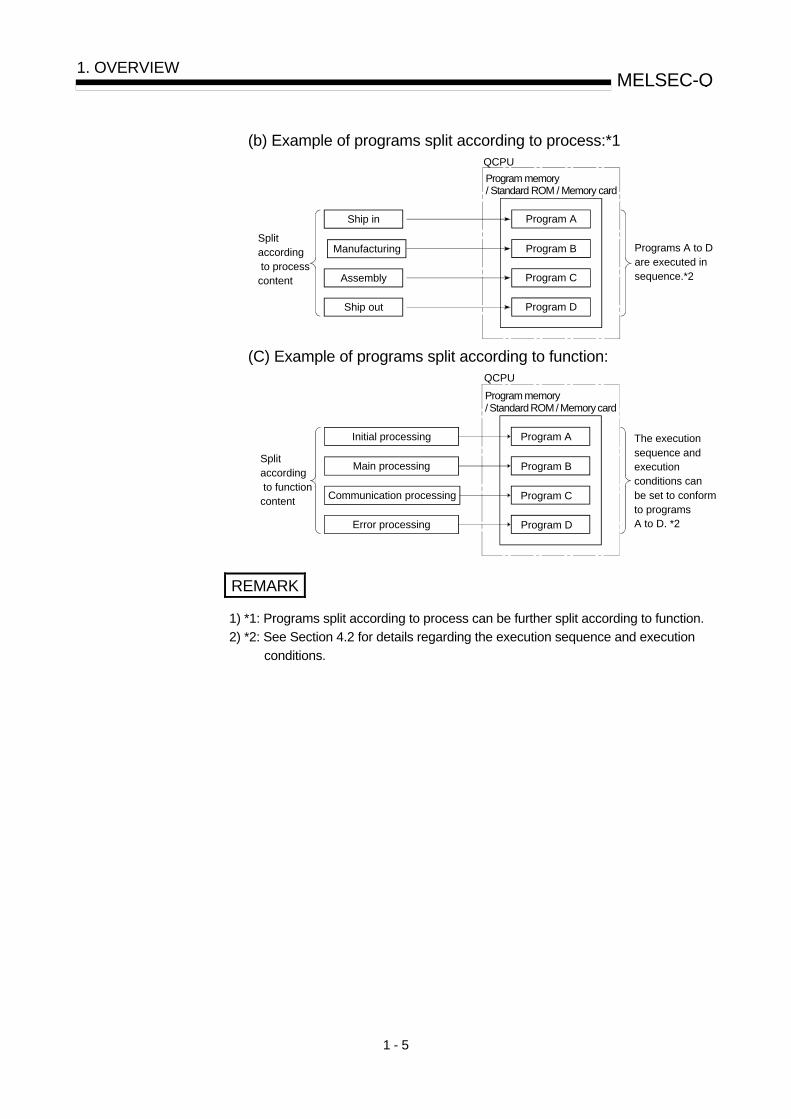
(b) Example of programs split according to process:*1
Split according to process content
Programs A to D are executed in sequence.*2
Ship in
Manufacturing
Assembly
Ship out
QCPU
Program A
Program B
Program C
Program D
Program memory/ Standard ROM / Memory card
(C) Example of programs split according to function:
Program memory / Standard ROM / Memory card
Split according to function content
The execution sequence and execution conditions can be set to conformto programs A to D. *2
Initial processing
Main processing
Communication processing
Error processing
QCPU
Program A
Program B
Program C
Program D
REMARK
1) *1: Programs split according to process can be further split according to function.
2) *2: See Section 4.2 for details regarding the execution sequence and execution
conditions.

1 - 6
MELSEC-Q 1. OVERVIEW
1.3 Convenient Programming Devices and Instructions
The QCPU features devices and instructions which facilitate program creation. A few
of these are described below.
(1) Flexible device designation
(a) Word device bits can be designated to serve as contacts or coils.
Switches b10 of D0 ON and OFF (1/0).The 1/0 status
of b5 of D0 is used as ON/OFF data.
b13
D0
b14b15 b12 b11b10
1/0
b9 b8 b7 b6 b5
1/0
b4 b3 b2 b1 b0
[For the case of QCPU]
X0 D0.5D0.A
[For the case of AnS]
X0K4M0
D0
D0MOV
K4M0MOV
M5M10
*
* : D0.5Bit designation
Word device designation
Bit designation of word device
(b) Direct processing in 1-point units is possible within a program simply by using
direct access inputs (DX ) and direct access outputs (DY ).
Output to output module at instruction execution
[For the case of QCPU]
M0 DX10DY100
[For the case of AnS]
M9036
K1B0
K1B0
K1X10SEG
K1Y100SEG
X10Y100
M9036M9052SET
M0
M9036
(X10 to X13 refresh)
(Y100 to Y103 refresh)
(Always ON)
Read from input module at instruction execution
Direct access input
(c) Differential contacts ( / ) eliminate the need for converting inputs to
pulses.
ON at leading edge of X0
[For the case of QCPU]
X0 X1Y100
[For the case of AnS]
M0
X0M0PLS
Y100
Y100
X1Y100
Differential contact

1 - 7
MELSEC-Q 1. OVERVIEW
(d) The buffer memory of intelligent function module (e.g. Q64AD, Q62DA) can
be used in the same way as devices when programming.
Readout of Q64AD buffer memory's address 12 data
[For the case of QCPU]
X0
[For the case of AnS]
X0K1D10K12H4FROMP
D0D10+P
D0U4\G12+P
* :U4\G12Buffer memory addressdesignation
Intelligent function module designation
*
Input/output Nos.:X/Y40 to X/Y4f
Pow
er s
uppl
y m
odul
eQ
CP
UIn
put (
16 p
oint
s)In
put (
16 p
oint
s)In
put (
16 p
oint
s)Q
64A
D (
16 p
oint
s)Q
64A
D (
16 p
oint
s)Q
62A
D (
16 p
oint
s)O
utpu
t (16
poi
nts)
Out
put (
16 p
oint
s)
Power supply module
(e) Direct access to link devices (LX, LY, LB, LW, LSB, LSW) of
MELSECNET/10H network modules (e.g. QJ71LP21) is possible without
refresh settings.
Direct readout of the No.5 network module's "LW12" link register
X0D0J5\W12+P
Network No.5
*
* :J5\W12Link register designation
Network No. designation
Pow
er s
uppl
y m
odul
eQ
CP
UQ
J71L
P21
Inpu
t (16
poi
nts)
Inpu
t (16
poi
nts)
Q68
AD
(16
poi
nts)
Q68
AD
(16
poi
nts)
Q62
AD
(16
poi
nts)
Out
put (
16 p
oint
s)O
utpu
t (16
poi
nts)
1 - 8
MELSEC-Q 1. OVERVIEW
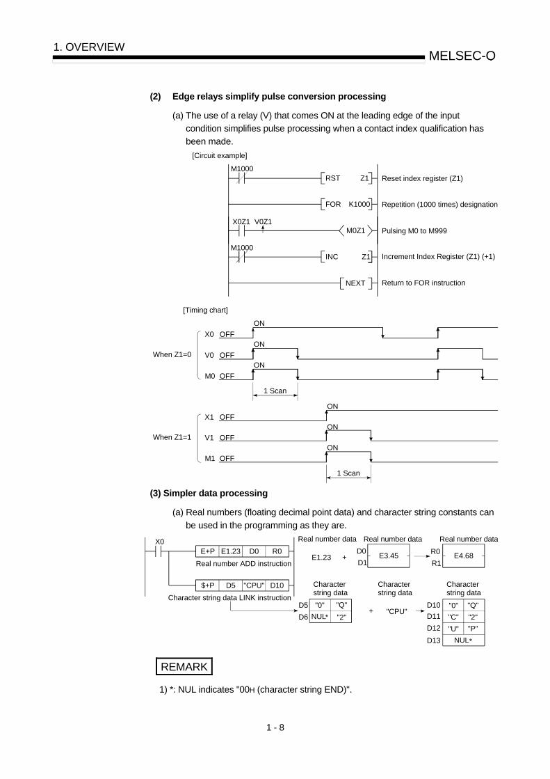
(2) Edge relays simplify pulse conversion processing
(a) The use of a relay (V) that comes ON at the leading edge of the input
condition simplifies pulse processing when a contact index qualification has
been made.
X0Z1 V0Z1M0Z1
K1000FOR
Z1RST
Z1INC
NEXT
M1000
M1000
[Circuit example]
Reset index register (Z1)
Repetition (1000 times) designation
Pulsing M0 to M999
Increment Index Register (Z1) (+1)
Return to FOR instruction
When Z1=0
X0 OFF
V0 OFF
M0 OFF
ON
ON
ON
1 Scan
[Timing chart]
When Z1=1
X1 OFF
V1 OFF
M1 OFF
ON
ON
ON
1 Scan
(3) Simpler data processing
(a) Real numbers (floating decimal point data) and character string constants can
be used in the programming as they are.
X0R0D0E1.23E+P
D10D5$+P
Real number ADD instruction
Character string data LINK instruction
Real number data
D0
Real number data
D1E3.45
R0
Real number data
R1E4.68+E1.23
"CPU"
D5
Character string data
D6
"0" "Q"
"2"+
D10
D11
D12
"0" "Q"
"C" "2"
"U" "P"
"CPU"NUL*
NUL*D13
Character string data
Character string data
REMARK
1) *: NUL indicates "00H (character string END)".

1 - 9
MELSEC-Q 1. OVERVIEW
(b) Data processing instructions such as table processing instructions, etc.,
enable high-speed processing of large amounts of data.
X0K2R0D0FINSP
Insertion source
R0
FIF0 table
R1
R2
R3
3
10
20
30
R4
Insertion designation
Insertion position R0
FIF0 table
R1
R2
R3
4
10
15
20
30R4
D0 15Instruction for data insertion at table
(4) Easy shared use of sub-routine programs
(a) A common pointer can be used to call the same sub-routine program from all
sequence programs being executed.
Program A Subroutine program
R0K4X20MOV
SM400
AlwaysON
R0K4X0MOV
RET
M0
M0P1000
P1000 call
Program B
P1000 callM10
P1000CALLP0
M0
P1000CALLP0
Common pointer
(b) The use of sub-routine call instructions with arguments simplifies the creation
of sub-routine programs which are called several times.
Sub-routine program
FD2FD1MOV
SM400FD2FD0MOV
RET
M0
M0P0
P0 call
Argument designationP0 callM10
100
M0R0K4X00 W0P0CALLP
R10K4X10W10P0CALLP
AlwaysON
Argument from FD2Argument to FD1Argument to FD0
Argument from FD2Argument to FD1Argument to FD0
Argument designation
*
*
Subroutine program designation
source dataDestination data
REMARK
* For details regarding the argument input/output condition, refer to Section 10.3.1.

1 - 10
MELSEC-Q 1. OVERVIEW
MEMO

2 - 1
MELSEC-Q 2. SYSTEM CONFIGURATION
2
2. SYSTEM CONFIGURATION
This section describes the QCPU system configuration, system precaution and devices. 2.1 System Configuration
Describes the system equipment, peripheral device configuration and system
configuration overview related to the QCPU system.
(1) QCPU System Equipment
Memory card *1,*3(Q2MEM-1MBS, Q2MEM-2MBF,Q2MEM-4MBF,Q2MEM-8MBA,
Q2MEM-16MBA,Q2MEM-4MBA)
QCPU(Q02CPU,Q02HCPU,Q06HCPU,
Q12HCPU,Q25HCPU)
Battery (Q6BAT)
Main base unit(Q35B,Q38B,Q312B)
Power supply of the Q series / I/O module
/ Intelligent funciton module
Power supply of the Q series / I/O module
/ Intelligent funciton module
Extension cable(QC06B,QC12B,QC30B,
QC50B,QC100B)
Power supply of the AnS series / I/O module
/ Special funciton module
Extension of the AnS series module *2 Extension of the Q series module
MITSUBISHI
MITSUBISHILITHIUM BATTERY
*3 With commercial memory cards, the operation is not assured.
QA1S6 extension base unit(QA1S65B,QA1S68B)
Q6 B extension base unit(Q65B,Q68B,Q612B)
POINT *1: One memory card can be mounted as needed.
The memory card can be selected from SRAM, Flash and ATA according to the application and capacity.
*2: The QA1S65B and QA1S68B extension base units can be used for the AnS series power supply module, I/O module and special-function module.

2 - 2
MELSEC-Q 2. SYSTEM CONFIGURATION
(2) QCPU Peripheral Device Configurations
USB cable*2 (To be procured yourself)
Used only for Q02HCPU,Q06HCPU,Q12HCPU and Q25HCPU
Memory card*2 (Q2MEM-1MBS,Q2MEM-2MBF,Q2MEM-4MBF,Q2MEM-8MBA)
QCPU(Q02CPU,Q02HCPU,Q06HCPU,
Q12HCPU,Q25HCPU)
RS-232 cable (QC30R2)
PC card adapter(Q2MEM-ADP)
Personal computer (SW D5C-GPPW)*1
*1: The box indicates a version number of 4 or higher.
*2: See the GPPW Operating Manual for a procedure for writing in a memory
card and USB cables.

2 - 3
MELSEC-Q 2. SYSTEM CONFIGURATION
(3) System Configuration Overview
System
configuration
4 extension stages
2 extension stages
1 extension stages
6 extension stages
7 extension stages
5 extension stages
3 extension stages
100
11F
120
13F
140
15F
160
17F
Pow
er s
uppl
y m
odul
e
20
3F
40
5F
60
7F
80
9F
A0
BF
C0
DF
E0
FF
0 1 2 3 4 5 6 7 8 9 10 11Main base unit (Q312B)
Slot No.
C P
U
OU
T
00
1F
2A0
2BF
2C0
2DF
2E0
2FF
Pow
er s
uppl
y m
odul
e
1C0
1DF
1E0
1FF
200
21F
220
23F
240
25F
260
27F
280
29F
13 14 15 16 17 18 19 20 21 22 23Extenison base unit (Q612B)
IN
1A0
1BFOU
T
180
19F
12P
ower
sup
ply
mod
ule
340
35F
360
37F
380
39F
3A0
3BF
3C0
3DF
3E0
3FF
25 26 27 28 29 30 31Extension base unit (Q68B)
IN
320
33FOU
T
300
31F
24
Pow
er s
uppl
y m
odul
e
440
45F
460
47F
480
49F
4A0
4BF
4C0
4DF
3E0
4FF
33 34 35 36 37 38 39Extension base unit (Q68B)
IN
420
43FOU
T
400
41F
32
Pow
er s
uppl
y m
odul
e
540
55F
560
57F
580
59F
41 42 43 44Extension base unit (Q65B)
IN
520
53FOU
T
500
51F
40
Pow
er s
uppl
y m
odul
e
5E0
5FF
600
61F
620
63F
640
65F
660
67F
680
69F
46 47 48 49 50 51 52Extension base unit (QA1S68B)
IN
5C0
5DFOU
T
5A0
5BF
45
Pow
er s
uppl
y m
odul
e
6E0
6FF
700
71F
720
73F
740
75F
760
77F
780
79F
54 55 56 57 58 59 60Extension base unit (QA1S68B)
IN
6C0
6DFOU
T
6A0
6BF
53
Pow
er s
uppl
y m
odul
e
7E0
7FF
62 63Extension base unit (QA1S65B)
IN
7C0
7DFOU
T
7A0
7B0
61P
rohib
it
When module is installed, an error occurs.
* The figure shows the configuration when 32-input/output modules are loaded to each slot.
Extension cable
Pro
hib
it
Maximum number
of extension stages 7 extension stages
Maximum number
of mounted
input/output
modules
64 modules
Maximum
number of
input/output
points
4096
Main base units Q35B, Q38B, Q312B
Extension base
units Q65B, Q68B, Q612B, QA1S65B, QA1S68B
Extension cables QC06B, QC12B, QC30B, QC100B
Notes
(1) A maximum of 7 extension base units can be mounted. (2) Do not use extension cable longer than 13.2 m (43.28 feet). (3) When using an extension cable, it should not be connected to or allowed to come close to the main circuit (high voltage and large current). (4) When setting the number of extension stages, set the number in ascending order to avoid setting the same number repeatedly. (5) If Q6 B and QA1S6 B are to be mounted on the same extension base unit, be sure to connect Q6 B at first and then QA1S6 .
Make the setting of the number of levels of an extension base unit, starting with Q6 B in a descending order. (6) Connect an extension cable between the OUT connector of an extension base unit and the IN connector of another extension base unit. (7) An error may occur if more than 64 expensed base units are mounted.

2 - 4
MELSEC-Q 2. SYSTEM CONFIGURATION
2.2 System Precaution
This section describes hardware and software packages compatible with QCPU.
(1) Hardware
(a) Number of allowable modules and functions are limited depending on
particular module.
Name Model name Number of modules/Limitation
Q series
MELSECNET/10H
network module
QJ71PL21, QJ71BR11 Up to 4
Q series Ethernet
interface module QJ71E71, QJ71E71-B2 Up to 4
Q series CC-Link system
master/local module QJ61BT11 Up to 4
MELSECNET/MINI-S3
data link module A1SJ71PT32-S3, A1SJ71T32-S3
No limitation (However, auto
refresh function can not be set.)
AnS series special-
function module shown on
the right
A1SD51S, A1SD21-S1,
A1SJ71J92-S3
(On the GET/PUT service)
Up to the total 6
Interrupt module A1SI61 Only one
Ethernet is a registered trademark of XEROX in the U.S.
(b) The following AnS Series special-function modules are limited in the range of
accessible devices:
• A1SJ71ME81 Type ME-Net Interface Module
• A1S71J92-S3 Type JEMANET Interface Module
• A1SD51S Type Intelligent Communications Unit
Devic Accessible device range
Input (X), output (Y) X/Y0 to 7FF
Internal relay (M) M0 to 8191
Latch relay (L) L0 to 8191
Link relay (B) B0 to FFF
Timer (T) T0 to 2047
Counter (C) C0 to 1023
Date register (D) D0 to 6143
Link register (W) W0 to FFF
Annunciator (F) F0 to 2047
(c) A graphic operation terminal can be used only for the GOT900 series.
It requires installation of a Q-mode compatible operating system (OS) and a
communications driver.
Bus connections cannot be made because a Q-Series bus interface is not
provided. GOT800 Series, A77GOT, and A64GOT cannot be used.

2 - 5
MELSEC-Q 2. SYSTEM CONFIGURATION
(d) The following modules can not be used by QCPU:
Name Model name
MELSECNET/10 network module A1SJ71LP21, A1SJ71BR11, A1SJ71QLP21,
A1SJ71QLP21S, A1SJ71QLP21GE, A1SJ71QBR11
MELSECNET(II),/B data link module A1SJ71AP21, A1SJ71AR21, A1SJ71AT21B
Ethernet interface module A1SJ71QE71-B2 (-B5), A1SJ71E71-B2-S3 (-B5-S3)
Serial communication module,
computer link module A1SJ71QC24(N), A1SJ71UC24-R2 (-R4/-PRF)
CC-Link master/local module A1SJ61QBT11, A1SJ61BT11
Modem interface module A1SJ71CMO-S3
ME-NET interface module A1SJ71ME81
(e) QCPU does not process unit-specific instructions for the following units
although they are included in QnA/A Series program instructions. This
requires that the user must rewrite FROM/TO instructions.
Name Model name
High-speed counter module A1SD61, A1SD62, A1SD62D(-S1), A1SD62E
MELSECNET/MINI-S3 A1SJ71PT32, A1SJ71T32-S3
Positioning module A1SD75P1-S3 (P2-S3/P3-S3), A1SD75M1 (M2/M3)
ID module A1SJ71ID1-R4, A1SJ71ID2-R4
(2) Software package
The following is QCPU system startup software packages for program creation:
• Q-series compatible GPPW (later than SW4D5C-GPPW)

2 - 6
MELSEC-Q 2. SYSTEM CONFIGURATION
MEMO

3 - 1
MELSEC-Q 3. PERFORMANCE SPECIFICATION
3
3. PERFORMANCE SPECIFICATION
Performance specification of QCPU module is as follows:
Table 3.1 Performance specification
Model name Item
Q02CPU Q02HCPU Q06HCPU Q12HCPU Q25HCPU Remark
Control method Repetitive operation of stored program
I/O control method Refresh mode
Direct I/O is
available via
device name
Sequence control dedicated language
Program language Relay symbol language, logic symbolic language,
MELSAP-3 (SFC)
LD 0.079 0.034 Processing speed (sequence
instructions) ( s/step) MOV 0.237 0.102
Number of instructions 360 (except intelligent function module dedicated instruction)
Constant scan (ms)
(program start at a specified interval) 0.5 to 2000 (configurable in multiple of 0.5 ms)
Set parameter
values to specify
Program capacity
(steps)
Program memory
(drive 0) 28k 60k 124k 252k See Section 6.2
Memory card
(RAM) (drive 1) Capacity of loading memory cards (1 M maximum) See Section 6.5
Memory card
(ROM) (drive 2)
Capacity of loading memory cards
(Flash card: 4 M maximum, ATA card 32 M maximum) See Section 6.5
Standard RAM
(drive 3) 64k See Section 6.4
Memory capacity
(bites)
Standard ROM
(drive 4) 112k 240k 496k 1008k See Section 6.3
Program memory 28 60 124 252* See Section 6.2
Memory card
(RAM) 256 See Section 6.5
Flash
card 288 See Section 6.5 Memory
card
(ROM) ATA
card 512 See Section 6.5
Standard RAM 2
1 file each for file
register and local
device, see
Section 6.4
Maximum number
of stored files
(files)
Standard ROM 28 60 124 252 See Section 6.3
I/O device points (points) 8192 (X/Y0 to 1FFF) Number of usable
points in program
I/O points (points) 4096 (X/Y0 to FFF)
Number of points
accessible to actual
I/O modules
*: Maximum number of executable program is 124. More than 124 programs can not be executed.

3 - 2
MELSEC-Q 3. PERFORMANCE SPECIFICATION
Table 3.1 Performance specification (continued)
Model name Item
Q02CPU Q02HCPU Q06HCPU Q12HCPU Q25HCPU Remark
Internal relay [M] (points) Default 8192 (M0 to 8191)
Latch relay [L] (points) Default 8192 (L0 to 8191)
Link relay [B] (points) Default 8192 (B0 to 1FFF)
Timer [ T ] (points)
Default 2048 (T0 to 2047) (for low/high speed timer)
Select between low/high speed timer by instruction
Set the measurement module of low/high speed timer by parameter
(Low speed timer: 1 to 1000 ms, 1 ms/module, default 100 ms)
(High speed timer: 0.1 to 100ms, 0.1 ms/module, default 10 ms)
Retentive timer [ST] (points)
Default 0 (for low/high speed timer)
Select between low/high speed retentive timer by instruction
Set the measurement module of low/high speed retentive timer
by parameter
(Low speed retentive timer: 1 to 1000 ms, 1 ms/module, default
100 ms)
(High speed retentive timer: 0.1 to 100ms, 0.1 ms/module,
default 10 ms)
Counter [C] (points) • Normal counter default 1024 (C0 to 1023)
• Interrupt counter maximum 256 (default 0 point, set via parameter)
Data register [D] (points) Default 12288 (D0 to 12287)
Link register [W] (points) Default 8192 (W0 to 1FFF)
Annunciator [F] (points) Default 2048 (F0 to 2047)
Edge relay [V] (points) Default 2048 (V0 to 2047)
Set parameter
values to specify
usable point
[R] (points)
• When standard RAM is used: 32768 (R0 to 32768)
• When standard SRAM card is used:
may use up to maximum of 517120 points by block
conversion by 32768 (R0 to 32767) unit
• When flash card (2 Mbyte) is used:
may use up to maximum of 1040384 points by block
conversion by 32768 (R0 to 32767) unit
• When flash card (4 Mbyte) is used:
may use up to maximum of 1042432 points by block
conversion by 32768 (R0 to 32767) unit
Num
ber
of d
evic
e po
ints
File register
[ZR] (points)
• When standard RAM is used: 32768 (ZR0 to 32767)
• When standard SRAM card is used:
517120 (ZR0 to 517119), no block conversion necessary
• When flash card (2 Mbyte) is used:
1040384 (ZR0 to 1040383), no block conversion necessary
• When flash card (4 Mbyte) is used:
1042432 (ZR0 to 1042431), no block conversion necessary
When flash card
is used, only read
process is
enabled

3 - 3
MELSEC-Q 3. PERFORMANCE SPECIFICATION
Table 3.1 Performance specification (continued)
Model name Item
Q02CPU Q02HCPU Q06HCPU Q12HCPU Q25HCPU Remark
Special link relay [SB] (points) 2048 (SB0 to 7FF)
Special link register [SW] (points) 2048 (SW0 to 7FF)
Step relay [S] (points) 8192 (S0 to 8191)
Index register [Z] (points) 16 (Z0 to 15)
Pointer [P] (points) 4096 (P0 to 4095), set parameter values to select usable range
of in-file pointer/shared pointers
Interrupt pointer [I] (points)
256 (IO to 255)
set parameter values to select periodic interval of system
interrupt pointers I28 to I31 (0.5 to 1000 ms, 0.5 ms modules)
default I28: 100ms I29: 40ms I30: 20ms I31: 10ms
Number of device
points is fixed.
Special relay [SM] (points) 2048 (SM0 to 2047)
Special register [SD] (points) 2048 (SD0 to 2047)
Function input [FX] (points) 16 (FX0 to F)
Function output [FY] (points) 16 (FY0 to F)
Num
ber
of d
evic
e po
ints
Function register [FD] (points) 5 (FD0 to 4)
Number of device
points is fixed.
Link direct device
Device for direct access of link devices.
For MELSECNET/10H use only.
Specified form : J \W , J \B , J \SW ,
J \SB
Intelligent function module device Device for direct access of intelligent function module buffer
memory. Specified form : U \G ,
Latch (power failure compensation)
range
L0 to 8191 (default)
(Latch range may be specified for B, F, V, T, ST, C, D, W)
Remote RUN/PAUSE contact points May specify one RUN/PAUSE contact point each by X0 to 1FFF.
Set parameter
values to specify
Clock function
Year, month, date, hour, minute, second, day of week
(auto-detects leap years)
Accuracy : -3.18 to +5.25s (TYP. +2.12s)/d at 0 C
Accuracy : -3.93 to +5.25s (TYP. +1.90s)/d at 25 C
Accuracy : -14.69 to +3.53s (TYP. -3.67s)/d at 55 C
Allowable momentary power failure
period By power supply module
5.V.DC internal current consumption (A) 0.60 0.64 0.64 0.64 0.64
Mass [kg (lb)] 0.20 (0.44) 0.20 (0.44) 0.20 (0.44) 0.20 (0.44) 0.20 (0.44)
External dimension [mm (in)} 98 (H) × 27.4 (W) × 89.3 (D) (3.86 × 1.08 × 3.52)
REMARK
Refer to the QCPU (Q Mode) User's Manual (Hardware Design/Maintenance and
Inspection), for details for QCPU general specification.

3 - 4
MELSEC-Q 3. PERFORMANCE SPECIFICATION
MEMO

4 - 1
MELSEC-Q 4. SEQUENCE PROGRAM CONFIGURATION & EXECUTION CONDITIONS
4
4. SEQUENCE PROGRAM CONFIGURATION & EXECUTION CONDITIONS
Sequence programs and SFC programs can be executed at the QCPU. This chapter describes the sequence program configuration and execution conditions. SFC programs are not described in this manual. For details regarding SFC programs, refer to the QCPU (Q mode)/QnACPU Programming Manual (SFC).
4.1 Sequence Program
(1) Definition of sequence program
(a) A sequence program is created using QCPU sequence instructions, basic instructions, and application instructions, etc.
Sequence instruction
T0
X0
X1
X41
M0 K100T0
Y30
BIN K4X10 D0
FROM H5 K0 D10 K1
Basic instruction
Application instruction
(b) There are 3 types of sequence program: main routine programs, sub-routine programs, and interrupt programs. For details regarding these programs, refer to the following sections of this manual: • Main routine programs : Section 4.1.1 • Sub-routine programs : Section 4.1.2 • Interrupt programs : Section 4.1.3
File A
Main routine program
Sub-routine program
FEND
Interrupt program
RET
IRET
END
P0
I0
REMARK
1) For details regarding the QCPU sequence instructions, basic instructions, and
application instructions, refer to the " QCPU (Q Mode)/QnACPU Programming
Manual (Common Instructions)".

4 - 2
MELSEC-Q 4. SEQUENCE PROGRAM CONFIGURATION & EXECUTION CONDITIONS
(2) Sequence program writing format
Programming for sequence programs is possible using either ladder mode, or list
mode.
(a) Ladder mode • The ladder mode is based on the relay control sequence ladder.
Programming expressions are similar to the relay control sequence ladder. • Relay symbolic language programming occurs in ladder block units.
A ladder block is the smallest unit of sequence program processing, with the ladder beginning from the left bus and ending at the right bus.
Y21
Y22
Y23
Y24
X1
Y20
X2 X3
X4 X5
Y24
X00
2
8
Left bus
Step No.
Right bus
Ladder blocks
*X0 to X5 : Indicate inputs. Y20 to Y24 : Indicate outputs.
a Contact b Contact Coil (output)
Fig.4.1 Ladder Block
(b) List mode The list mode uses dedicated instructions instead of the contact symbols, coil symbols, etc., used in the ladder mode. Contact a, contact b and coil instructions are as follows:
• a contact ............LD, AND, OR
• b contact ............LDI, ANI, ORI
• coil......................OUT
(2) Program processing
Sequence programs are processed in order, beginning from step 0 and ending at the END/FEND instruction. Processing of ladder mode ladder blocks begins from the left bus, and proceeds from left to right. When one ladder block is completed, processing proceeds downward to the next ladder block.
0 LD 1 AND 2 LD 3 AND 4 ORB 5 OR 6 AND 7 AND 8 AND 9 OUT 10 END
Top to bottom
*Numbers 1) to 11) indicate the processing order of the sequence program.
[Ladder mode]
Left to right
1)X0
2)X1
7)X5
8)X6
9)X7
3)X2
4)X3
6)X4
10)Y100
10
5)
11)END
[List mode]
Executed in order, beginning from step 0 to the ending at the END instruction.
Step No.
X0X1X2X3 X4X5X6X7 Y10
1) 2) 3) 4) 5) 6) 7) 8) 9)10)11)
Fig.4.2 Sequence Program Processing

4 - 3
MELSEC-Q 4. SEQUENCE PROGRAM CONFIGURATION & EXECUTION CONDITIONS
4.1.1 Main routine program
(1) Definition of main routine program
(a) A main routine program is a program which begins from step 0 and ends at
the END/FEND instruction. *1
(b) The main routine program execution begins from step 0 and ends at the
END/FEND instruction.
1) If only one program is being executed, processing will begin from step 0
again after the END/FEND instruction is processed.
END/FEND
Main routine program
Step 0
END/FEND
END processing
Program execution
Returns to step 0 when only one program is being executed.
2) If multiple programs are being executed, processing which occurs after
the END/FEND instruction varies according to the designated execution
conditions.
(2) Execution conditions for main routine programs *2
If multiple programs are being executed, the following five types of execution
conditions can be designated by the program in the PLC parameters according to
the application in question.
• Initial execution program : See Section 4.2.1.
• Scan execution type program : See Section 4.2.2.
• Low-speed execution program : See Section 4.2.3.
• Stand-by type program : See Section 4.2.4.
• Fixed scan execution type program : See Section 4.2.5.
REMARK
1) *1: For details regarding the END/FEND instruction, refer to the "QCPU (Q
mode)/QnACPU Programming Manual (Common Instructions)".
2) *2: If only one program is executed, it is processed under the "scan execution type
program" condition without designation by the program in the PLC parameters.

4 - 4
MELSEC-Q 4. SEQUENCE PROGRAM CONFIGURATION & EXECUTION CONDITIONS
4.1.2 Sub-routine programs
(1) Definition of sub-routine program
(a) A sub-routine program is a program which begins from a pointer (P ) and
ends at a RET instruction. (b) A sub-routine program is executed only when called by a CALL instruction
(e.g. CALL(P), FCALL(P)) from the main routine program.
(c) Sub-routine program application 1) The overall step count can be reduced by using a sub-routine program
as a program which is executed several times in one scan. 2) The step count of a constantly executed program can be reduced by
using a sub-routine program as a program which is executed only when a given condition is satisfied.
(2) Sub-routine program management
Sub-routine programs are created after the main program (after FEND instruction), and the combination of main and sub-routine programs can be managed as one program. (a) When created after the main program
• A sub-routine program is created between the main program's FEND and END instructions.
• Because there are no restrictions regarding the order in which sub-routine programs are created, there is no need to set the pointers in ascending order when creating multiple sub-routine programs.
• Either a local pointer or a common pointer may be used. *
Program A
Sub-routine program
Write
QCPU
Main routine program
FEND
END
P8
RET
RET
Y10
RET
Y11
Y12
P0
P1
Program memory / Standard ROM / Memory card
Program A
REMARK
1) *: See Section 10.9 for details regarding local and common pointers. 2) See Section 10.8 for details regarding sub-routine program nesting.

4 - 5
MELSEC-Q 4. SEQUENCE PROGRAM CONFIGURATION & EXECUTION CONDITIONS
(b) Using the sub-routine program as a separate program
Sub-routine programs can also be managed as separate, discrete programs
(stand-by type programs). (See Section 4.2.4 for details regarding stand-by
type programs).

4 - 6
MELSEC-Q 4. SEQUENCE PROGRAM CONFIGURATION & EXECUTION CONDITIONS
4.1.3 Interrupt programs
(1) Definition of interrupt program
(a) An interrupt program is a program which begins at the interrupt pointer (I ),
and ends at the IRET instruction. *1 (b) Interrupt programs are executed only when an interrupt factor occurs. *1
(2) Interrupt program management
Interrupt programs are created after the main program (after the FEND instruction), and the combination of main and sub-routine programs can be managed as one program.
(a) When created after the main program • An interrupt program is created between the main program's FEND and
END instructions. • Because there are no restrictions regarding the order in which interrupt
programs are created, there is no need to set the interrupt pointers in ascending order when creating multiple interrupt programs.
QCPU
Program memory/ StandardROM / Memory card
Program A
Program A
Interrupt program
Write
Interrupt pointer
Main routine program
FEND
END*2
I32
IRET
IRET
Y10
IRET
Y11
Y12
I0
I28
(b) Using the interrupt program as a separate program Interrupt programs can also be managed as separate, discrete programs (stand-by type programs). (See Section 4.2.4 for details regarding stand-by type programs). However, the same interrupt program pointer number cannot be used more than once in the program being executed by the QCPU.
REMARK
1) *1: See Section 10.10 for details regarding interrupt factors and interrupt pointers. 2) *2: An END instruction is needed at the last step of the interrupt program. Absence of
an END instruction may cause an "END NOT EXECUT" error.
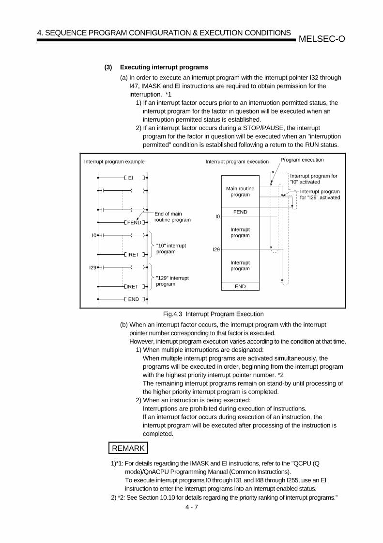
4 - 7
MELSEC-Q 4. SEQUENCE PROGRAM CONFIGURATION & EXECUTION CONDITIONS
(3) Executing interrupt programs
(a) In order to execute an interrupt program with the interrupt pointer I32 through I47, IMASK and EI instructions are required to obtain permission for the interruption. *1
1) If an interrupt factor occurs prior to an interruption permitted status, the interrupt program for the factor in question will be executed when an interruption permitted status is established.
2) If an interrupt factor occurs during a STOP/PAUSE, the interrupt program for the factor in question will be executed when an "interruption permitted" condition is established following a return to the RUN status.
Main routine program
FEND
Interrupt program
Interrupt program
END
Interrupt program for "I0" activated
Interrupt program for "I29" activated
Program execution
FEND
EI
IRET
IRET
END
"10" interrupt program
"129" interrupt program
End of main routine program
I0
I29
I0
I29
Interrupt program example Interrupt program execution
Fig.4.3 Interrupt Program Execution (b) When an interrupt factor occurs, the interrupt program with the interrupt
pointer number corresponding to that factor is executed. However, interrupt program execution varies according to the condition at that time.
1) When multiple interruptions are designated: When multiple interrupt programs are activated simultaneously, the programs will be executed in order, beginning from the interrupt program with the highest priority interrupt pointer number. *2 The remaining interrupt programs remain on stand-by until processing of the higher priority interrupt program is completed.
2) When an instruction is being executed: Interruptions are prohibited during execution of instructions. If an interrupt factor occurs during execution of an instruction, the interrupt program will be executed after processing of the instruction is completed.
REMARK
1)*1: For details regarding the IMASK and EI instructions, refer to the "QCPU (Q mode)/QnACPU Programming Manual (Common Instructions). To execute interrupt programs I0 through I31 and I48 through I255, use an EI instruction to enter the interrupt programs into an interrupt enabled status.
2) *2: See Section 10.10 for details regarding the priority ranking of interrupt programs.”

4 - 8
MELSEC-Q 4. SEQUENCE PROGRAM CONFIGURATION & EXECUTION CONDITIONS
3) Interruption during a network refresh:
If an interrupt factor occurs during a network refresh operation, the network refresh operation is suspended, and the interrupt program is executed. This means that "assurance of blocks in cyclic data at each station" cannot be secured by using a device designated as a destination of link refresh operation on the MESSECNET/10H Network System. *1
Interrupt factor
Interrupt programexecution
Network refreshexecution
10ms 10ms 10ms 10ms
Network refresh operation is suspended, and the interrupt program is executed.
Fig.4.4 Interruption during Network Refresh Operation
4) Interruption during END processing:
If an interrupt factor occurs during an END processing waiting period
during constant scanning, the interrupt program corresponding to that
factor will be executed.
(c) See Section 10.6.2 for details regarding index register processing when
switching to an interrupt program from a scan execution type program or low-
speed execution program.
(4) High-speed execution of an interrupt program and overhead time
By default, QCPU will perform the following process when executing an interrupt
program:
• To hide and restore an index register.
• To hide and restore the file name of a file register in use.
The above-listed processes are not performed if an option to "Execute at a High
Speed" is selected in the PLC System Setting sheet of the PLC Parameter dialog box.
This will make it possible to shorten the duration of overhead time required for
execution of an interrupt program. OVERHEAD TIME ( s)
CPU TYPE LOW-SPEED EXECUTION HIGH-SPEED EXECUTION
Q02CPU 380 230
Q02HCPU, Q06HCPU,
Q12HCPU, Q25HCPU 165 100
REMARK
*1: For assurance of station unit blocks in cyclic data, see the "Reference Manual for the Q-Compatible MELECNET/10H Network System."

4 - 9
MELSEC-Q 4. SEQUENCE PROGRAM CONFIGURATION & EXECUTION CONDITIONS
(5) Program creation restrictions
(a) A device which is switched ON by a PLS instruction in an interrupt program
will remain ON until that interrupt program is executed again.
X0 OFF
ON
M0 OFF
ON
END 0 IO IRET END 0 END 0 IO IRET END 0
PLS M0X0
PLS M0X0
Switched OFF by PLS M0 instruction
Switched ON by PLS M0 instruction at X0 leading edge (OFF to ON)
(b) A DI status (interruption prohibited) is established during execution of an
interrupt program.
Do not execute EI/DI instructions in the interrupt program.
(c) Timers cannot be used in interrupt programs. As timers are used at OUT T instructions to update present values and
switch contacts ON and OFF, the use of a timer in the interrupt program
would make a normal time count impossible.

4 - 10
MELSEC-Q 4. SEQUENCE PROGRAM CONFIGURATION & EXECUTION CONDITIONS
4.2 Program Execute Type
Programs executed by the QCPU can be stored in the QCPU's program memory,
standard ROM or memory card.
Programs can be stored in the standard ROM or memory card as a single program, but
also as multiple programs by splitting them into separate programs for each control
function.
This permits the programming procedure to be split up among several program
designers, who can design separate programs for each operation and can store them
in the standard ROM or memory card.
When multiple programs are executed by the QCPU, "program name (file name)" and
"execute type" settings of the programs must be designated.
Control contents A
Control by separating into multiple programs
Program A
Control contents B
Program B
Control contents n
Program n
Control contents A
Control by one program
Control contents B
Control contents n
Store by separating the code according to control contents.
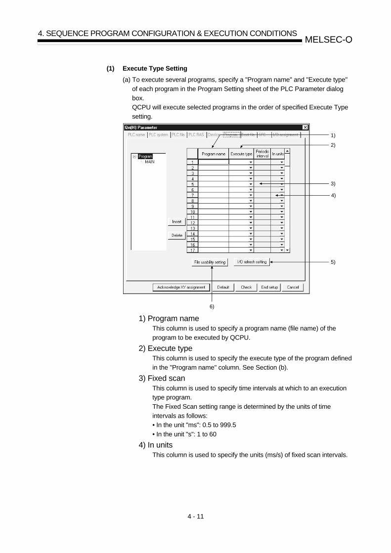
4 - 11
MELSEC-Q 4. SEQUENCE PROGRAM CONFIGURATION & EXECUTION CONDITIONS
(1) Execute Type Setting
(a) To execute several programs, specify a "Program name" and "Execute type"
of each program in the Program Setting sheet of the PLC Parameter dialog
box.
QCPU will execute selected programs in the order of specified Execute Type
setting.
6)
5)
4)
3)
2)
1)
1) Program name This column is used to specify a program name (file name) of the
program to be executed by QCPU. 2) Execute type
This column is used to specify the execute type of the program defined
in the "Program name" column. See Section (b). 3) Fixed scan
This column is used to specify time intervals at which to an execution
type program.
The Fixed Scan setting range is determined by the units of time
intervals as follows:
• In the unit "ms": 0.5 to 999.5
• In the unit "s": 1 to 60 4) In units
This column is used to specify the units (ms/s) of fixed scan intervals.

4 - 12
MELSEC-Q 4. SEQUENCE PROGRAM CONFIGURATION & EXECUTION CONDITIONS
5) File Use Setting
The PLC File Setting sheet of the PLC Setting dialog box has several
options: file register, device's initial value, comment, and local device.
Specify whether to use files of these options for each program. By
default, the option "Use PLC file setting" is selected. If the option "Not
used" is selected, the File Use setting is made as listed below in the table.
Setting item Processing when the option "Not used" is selected
File register File registers can not be used in the program.
Device initial value The device initial value is not set when the program file name and
the device initial value is the same.
Comment Comments can not be used in the program.
Local device Local devices are not hidden or restored at the time of program
conversion.
6) I/O Refresh Setting QCPU uses the I/O Refresh setting to update output and input from an
I/O module and an intelligent-function module.
The I/O Refresh Setting button is used to update the range of selected
programs. Make the I/O Refresh setting for a scan execution type
program if you want to receive an input (X) or produce an output (Y)
before executing the fixed scan execution type program.
(b) There are following 5 execute types: 1) Initial execution (Initial)
This program type is executed once only at power ON or when STOP-
RUN switching occurs. (See Section 4.2.1) 2) Scan execution (Scan)
This program type is executed once per scan, beginning from the scan
which follows execution of the initial execution program. (See Section 4.2.2) 3) Low-speed execution (Low speed)
This program type is executed only when a constant scan setting is
made or when a time is set for execution of low-speed execution
programs.
• When a constant scan setting is made, the program is executed
during the surplus time of a scan execution type program.
• When a time for execution of low-speed execution programs is set,
the program is executed during this set time. (See Section 4.2.3.) 4) Stand-by (Wait)
This program is executed only when its execution is requested. See
Section (4.2.4.) 5) Fixed scan execution (Fixed scan)
Program that is executed at time intervals specified in the "Fixed scan"
and "In units" columns of the Program Setting sheet of the PLC
Parameter dialog box. (See Section 4.2.5.) (c) Scantimes of programs being executed (except the fixed scan execution type
program) can be checked on the monitor of the program list. (See Section 7.11.1.)

4 - 13
MELSEC-Q 4. SEQUENCE PROGRAM CONFIGURATION & EXECUTION CONDITIONS
(2) The program operation steps which occur at power ON or STOP to RUN
switching are shown below.
Initial execution type program
*
Executed only once at power ON or STOP to RUN.
END processing
Scan type program
Run only when execution request is given.
Low-speed execution type program
*
Run only when "constant scan" or
"low-speed program execution time"
has been set.
Stand-by type program
*
Power ON/STOP to RUN
Program run at specified cyclic time intervals
Cyclic execution type program
*
POINT
(1) Not all execute types need to be set for the QCPU.
Use the items marked with "*" as needed, such as the Initial execution, low-
speed execution, stand-by and fixed scan execution type programs.
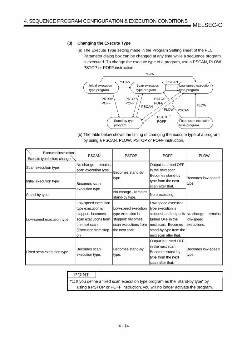
4 - 14
MELSEC-Q 4. SEQUENCE PROGRAM CONFIGURATION & EXECUTION CONDITIONS
(3) Changing the Execute Type
(a) The Execute Type setting made in the Program Setting sheet of the PLC
Parameter dialog box can be changed at any time while a sequence program
is executed. To change the execute type of a program, use a PSCAN, PLOW,
PSTOP or POFF instruction.
Initial execution type program
Scan execution type program
Low-speed execution type program
Stand-by type program
Fixed scan execution type program
PSCANPSCAN
PLOW
PLOW
PSTOPPOFF
PSTOPPOFF
PSCAN
PSTOPPOFF
PSTOPPOFF
*1
PLOW
PSCAN
(b) The table below shows the timing of changing the execute type of a program
by using a PSCAN, PLOW, PSTOP or POFF instruction.
Executed instruction
Execute type before change PSCAN PSTOP POFF PLOW
Scan execution type No change - remains
scan execution type.
Initial execution type
Becomes stand-by
type.
Output is turned OFF
in the next scan.
Becomes stand-by
type from the next
scan after that.
Stand-by type
Becomes scan
execution type. No change - remains
stand-by type. No processing.
Becomes low-speed
type.
Low-speed execution type
Low-speed execution
type execution is
stopped: becomes
scan executions from
the next scan.
(Execution from step
0.)
Low-speed execution
type execution is
stopped: becomes
scan executions from
the next scan.
Low-speed execution
type execution is
stopped, and output is
turned OFF in the
next scan. Becomes
stand-by type from the
next scan after that.
No change - remains
low-speed
executions.
Fixed scan execution type Becomes scan
execution type.
Becomes stand-by
type.
Output is turned OFF
in the next scan.
Becomes stand-by
type from the next
scan after that.
Becomes low-speed
type.
POINT
*1: If you define a fixed scan execution type program as the "stand-by type" by
using a PSTOP or POFF instruction, you will no longer activate the program.
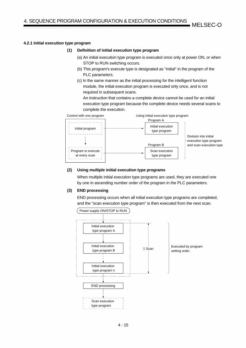
4 - 15
MELSEC-Q 4. SEQUENCE PROGRAM CONFIGURATION & EXECUTION CONDITIONS
4.2.1 Initial execution type program
(1) Definition of initial execution type program
(a) An initial execution type program is executed once only at power ON, or when
STOP to RUN switching occurs.
(b) This program's execute type is designated as "initial" in the program of the
PLC parameters.
(c) In the same manner as the initial processing for the intelligent function
module, the initial execution program is executed only once, and is not
required in subsequent scans.
An instruction that contains a complete device cannot be used for an initial
execution type program because the complete device needs several scans to
complete the execution.
Initial execution type program
Using initial execution type programProgram A
Scan execution type program
Program B
Initial program
Control with one program
Program to execute at every scan
Division into initial execution type program and scan execution type
(2) Using multiple initial execution type programs
When multiple initial execution type programs are used, they are executed one
by one in ascending number order of the program in the PLC parameters.
(3) END processing
END processing occurs when all initial execution type programs are completed,
and the "scan execution type program" is then executed from the next scan.
Initial execution type program A
Initial execution type program B
Initial execution type program n
END processing
Scan execution type program
Power supply ON/STOP to RUN
Executed by program setting order.
1 Scan

4 - 16
MELSEC-Q 4. SEQUENCE PROGRAM CONFIGURATION & EXECUTION CONDITIONS
(4) Initial scan time
(a) This is the execution time period for initial execution type programs. If multiple initial execution type programs are used, this is the execution time period in which all those programs are executed.
(b) The QCPU measures the initial scan time and stores the result in special
registers (SD522, SD523). *1 The initial scan time can therefore be checked by monitoring the SD522 and SD523 special registers.
Stores less than 1 ms initial scan time (unit s)
Stores the initial scan time in 1 ms units.
SD522 SD523
If the SD522 value is "3", and the SD523 value is "400", the initial scan time is 3.4 ms.
(5) Initial execution monitor time
The execution period of the initial execution type program can be monitored by this timer. The default value is not set. When monitoring the execution time of the initial execution type program, designate the Initial execution monitor time in a 10 ms to 2000 ms range at the PLC RAS settings in the PLC parameter. (Setting unit: 10 ms) When the initial scan time exceeds the set initial execution monitor time, "WDT ERROR" occurs, and QCPU operation is stopped.
POINT
(1)*1: The accuracy of the initial scan time stored at the special registers is ± 0.1 ms. The initial scan time count will continue even if a watchdog time reset instruction (WDT) is executed at the sequence program.
(2) When the initial execution monitor time is designated, there will be a 10 ms error in the count value. Therefore, a monitor time setting (t) of 10 ms will result in a "WDT ERROR" when the initial scan time is in the range 10 ms < t < 20 ms.

4 - 17
MELSEC-Q 4. SEQUENCE PROGRAM CONFIGURATION & EXECUTION CONDITIONS
4.2.2 Scan execution type program
(1) Definition of scan execution type program
(a) Scan execution type programs are executed once per scan, beginning from
the scan which follows execution of the initial execution type program.
(b) Set the execute type to "scan" in the program of PLC parameters.
(2) Executing multiple scan execution type programs
When multiple scan execution type programs are used, they are executed one by
one in ascending number order of the program in the PLC parameters.
(3) END processing
END processing occurs when all initial execution type programs are completed,
and the scan execution type program is then executed from the next scan.
The END processing (network refresh) can be performed for each program while
several scan execution type programs are executed. To do this, include a COM
instruction at the end of each scan execution type program.
First scan Second scan Third scan Forth scan
STOP to RUNPower ON to RUN
END processing
Initial execution type program
Scan execution type program A
Scan execution type program C
Scan execution type program B
Scan time
0 END
0 END
0 END
0 END
0 END
0 END
0 END
0
(4) Constant scan setting *1
When constant scanning is designated, the scan execution type program is
executed at each designated constant scan period.
REMARK
1)*1: The "constant scan" function executes the scan type program repeatedly at regular
intervals.
For details regarding of the constant scan, refer to Section 7.2.
POINT
(1) Refer to Section 10.6.2 for details regarding index register processing when an
interrupt program is executed while a scan execution type program is in
progress.

4 - 18
MELSEC-Q 4. SEQUENCE PROGRAM CONFIGURATION & EXECUTION CONDITIONS
(5) Scan time
(a) The "scan time" is a total of following the execution time of the scan execution
type program and END processing.
If multiple scan execution type programs are used, the "scan time" is the total
time required to execute all the programs.
(b) The scan time present value, minimum value, and maximum value are
measured at the QCPU, and the results are stored in special registers
(SD520, SD521, and SD524 to SD527). *1
The initial scan time can therefore be checked by monitoring the SD520,
SD521, and SD524 to SD527 special registers.
Stores less than 1 ms initial scan time (unit s)
Stores the initial scan time in 1 ms units.
SD520
SD524
SD526
Current value
Minimum value
Maximum value
SD521
SD525
SD527
If the SD520 value is 3, and the SD521 value is 400, the initial scan time is 3.4
ms.
(6) WDT (Watchdog timer)
This is the timer which monitors the scan time, and its default setting is 200 ms.
This WDT setting can be designated in a 10 ms to 2000 ms range in the PLC
RAS settings of the PLC parameter.
(Setting units: 10 ms)
When using the low-speed execution program, set the WDT greater than the
scan time plus the execution time of the low-speed execution program.
If the scan time (execution time for scan execution type program + low-speed
execution program) exceeds the WDT setting value, a "WDT ERROR" occurs,
and QCPU operation is stopped.
POINT
(1)*1: The accuracy of the scan time stored at the special registers is ± 0.1 ms.
The scan time count will continue even if a watchdog time reset instruction
(WDT) is executed at the sequence program.
(2) The WDT measurement error is 10 ms.
Therefore, a WDT setting (t) of 10 ms will result in a "WDT ERROR" if the scan
time is in the following range: 10 ms < t < 20 ms.
REMARK
1) Use the GPPW's Program Monitor List to check the execution time of a program
being executed. See Section 7.11.1 for further information on the GPPW's Program
Monitor List.

4 - 19
MELSEC-Q 4. SEQUENCE PROGRAM CONFIGURATION & EXECUTION CONDITIONS
4.2.3 Low-speed execution type program
(1) Definition of low-speed execution type program
(a) Low-speed execution type programs are executed only during "constant
scanning surplus time" or during the period designated for "low-speed
execution program execution time". 1) For a constant scan time with enhanced control accuracy, designate a
constant scan time setting at the PLC RAS in the PLC parameter. (Setting range: 0.5 to 2000 ms, setting units: 0.5 ms)
2) To secure execution time for low-speed execution type programs at each scan, designate a low-speed execution program execution time in the PLC RAS of the PLC parameter. (Setting range: 1 to 2000 ms, setting units: 1 ms)
3) In order to execute a low-speed execution type program, set either the constant scan time or low-speed execution program execution time.
(b) Set the execute type of the low-speed execution program to "low speed" in
the program of the PLC parameters.
(c) The low-speed execution type program is used for programs which do not
require execution in each scan, for example programs for printer output.
(2) Executing multiple low-speed execution type programs
When multiple low-speed execution type programs are used, they are executed
one by one in ascending number order of the program in the PLC parameters.
(3) Execution time of the Low-speed execution type program to be executed per scan
(a) If all the low-speed execution type program operation is completed within one scan and there is surplus time, the processing executed after that depends on the ON/OFF status of special register SM330 and the execution condition for low-speed execution type programs.
1) Asynchronous method (SM330 = OFF) Method in which low-speed execution type program operation is continued in the surplus time.
2) Synchronous method (SM330 = ON) Method in which even if there is surplus time, low-speed execution type program operation is not continued, and operation starts again from the next scan.
Execution condition for low-speed execution type programs Operation method for low-
speed execution type
programs
SM330
setting
status When constant scan time
is set
When low-speed execution
program execution time is set
Asynchronous method OFF
The low-speed execution
type program is re-
executed *1.
The low-speed execution type
program is re-executed *2.
Synchronous method ON Constant scan waiting
time is generated *3.
Scan execution type program
operation is started *4.
*1 If a constant scan time has been designated, the low-speed execution type program will be executed repeatedly during the constant scan's surplus time. Therefore, the low-speed execution type program's execution time varies from scan to scan. As the low-speed execution type program will not be executed at all if the constant scan's surplus time is 0.5 ms or less, a constant scan time setting should be designated which provides a surplus time of more than 0.5 ms.

4 - 20
MELSEC-Q 4. SEQUENCE PROGRAM CONFIGURATION & EXECUTION CONDITIONS
*2 If a low-speed execution type program execution time has been designated,
the low-speed execution type program will be executed repeatedly in
accordance with that time setting.
Therefore, the scan time will vary from scan to scan.
*3 If a constant scan time has been designated, the surplus time after completion
of low-speed END processing is waiting time, and execution of a scan
execution type program starts when the constant scan time has elapsed.
This means that the scan time is constant in each scan.
However, if the surplus time after the constant scan is less than 0.5 ms, low-
speed execution type programs cannot be executed. If using a low-speed
execution type program, set the constant scan time so that the surplus time is
0.5 ms or longer.
*4 If a "low-speed execution type program execution time" has been designated,
scan execution type program operation is started ignoring the surplus time
after completion of low-speed END processing.
This means that the scan time differs in each scan.
(b) If a low-speed execution type program cannot be processed within constant
scan surplus time or within the low-speed execution type program execution
time, program execution is temporarily stopped and the remainder of the
program is executed in the next scan.

4 - 21
MELSEC-Q 4. SEQUENCE PROGRAM CONFIGURATION & EXECUTION CONDITIONS
1 : Asynchronous method
(1) Constant scan time setting
The low-speed execution type program operation which occurs under the following conditions is illustrated below. • Constant scan time : 8ms • Total scan execution type program time : 4ms to 5ms • Execution time of low-speed type execution program A : 1ms • Execution time of low-speed execution type program B : 3ms • END processing/low-speed END processing : 0ms (0 ms is used to simplify the illustration)
0 8 16
END processing
24 (ms)
1ms
4.5ms
0.5ms
END processing
4ms
1ms
END processing
4ms
Low-speed scan time
Scan execution type program
Low-speed execution type program A
Low-speed execution type program B
END processing
4ms
Constant scan wait time0.5ms
0.5ms2.5ms 1.5ms 2ms
0.5ms
1.5ms
1ms
1ms
Low-speed END processing execution
0.5ms
1ms
Low-speed END processing execution
Low-speed END processing execution
Low-speed scan time
Low-speed scan time
(13ms) (8.5ms) (8.5ms)
(2) Low-speed execution program execution time setting
The low-speed execution type program operation which occurs under the following conditions is illustrated below. • Low-speed program execution time : 3ms • Total scan execution type program time : 4ms to 5ms • Execution time of low-speed type execution program A : 1ms • Execution time of low-speed execution type program B : 3ms • END processing/low-speed END processing : 0ms (0 ms is used to simplify the illustration)
0
END processing
END processing
18.5
END processing
25.5
END processing
33.5
END processing
(ms)
4ms
1ms
2ms
4.5ms
1ms
4ms
Low-speed scan time(8ms)
Low-speed scan time(12.5ms)
Low-speed END processing execution
Low-speed END processing execution
Scan execution type program
Low-speed execution type program A
Low-speed execution type program B
4 11.5
2ms
1ms1ms
1ms
1ms
Low-speed END processing execution
Low-speed scan time(8ms)
4ms 5ms
3ms

4 - 22
MELSEC-Q 4. SEQUENCE PROGRAM CONFIGURATION & EXECUTION CONDITIONS
2 : Synchronous method
(1) Constant scan time setting
The low-speed execution type program operation which occurs under the following conditions is illustrated below. • Constant scan time : 8ms • Total scan execution type program time : 4ms to 5ms • Execution time of low-speed type execution program A : 1ms • Execution time of low-speed execution type program B : 3ms • END processing/low-speed END processing : 0ms (0 ms is used to simplify the illustration)
0 8 16
END processing
24 32 (ms)
1ms
4.5ms
END processing
4ms
END processing
4ms 5ms
Low-speed scan time
Scan execution type program
Low-speed execution type program A
Low-speed execution type program B
END processing
4ms
Constant scan wait time0.5ms
2.5ms
Low-speed END processing execution
0.5ms
3ms
1ms
2.5ms
0.5ms
Low-speed END processing execution
0.5ms
3.5ms
Low-speed scan time
(13ms) (15.5ms)
(2) Low-speed execution program execution time setting
The low-speed execution type program operation which occurs under the following conditions is illustrated below. • Low-speed program execution time : 3ms • Total scan execution type program time : 4ms to 5ms • Execution time of low-speed type execution program A : 1ms • Execution time of low-speed execution type program B : 3ms • END processing : 0ms (0 ms is used to simplify the illustration)
0
END processing
END processing
16.5
END processing
23.5
END processing
29.5
END processing
(ms)
4ms
1ms
2ms
4.5ms
1ms
4ms
2ms
Low-speed scan time(12ms)
Low-speed scan time(12.5ms)
Low-speed END processing execution
Scan execution type program
Low-speed execution type program A
Low-speed execution type program B
4 11.5
1ms
1ms1ms
Low-speed END processing execution
5ms
2ms
4ms

4 - 23
MELSEC-Q 4. SEQUENCE PROGRAM CONFIGURATION & EXECUTION CONDITIONS
(4) Precautions for creating Low-speed execution type programs
(a) See Section 10.6.1 for details regarding index register processing when switching from a scan execution type program to a low-speed execution type program occurs.
(b) See Section 10.6.2 for details regarding index register processing when an interrupt program/a fixed scan execution type program is executed while a low-speed execution type program is in progress.
(c) The low-speed execution type program execution time setting should be such that the [scan time] + [low-speed execution type program execution time] sum is less than the WDT setting value.
(d) The COM instruction can not be used in low-speed execution type programs.
(5) Low-speed END processing
The low-speed END processing is performed when all the low-speed execution type programs are executed. The following processing is performed for the low-speed END processing. • Low-speed program special relay/special register setting • Low-speed execution program write during RUN • Low-speed scan time measurement • Low-speed execution type program watchdog timer reset
When the low-speed END processing is completed, the low-speed execution type program is executed from the beginning again.
POINT (1) During execution of low-speed execution type programs, the constant scan time
may deviate by the amount of "the maximum instruction processing time + low-speed END processing time".
(6) Low-speed scan time
(a) The low-speed scan time is the total time required for low-speed execution type program execution and low-speed END processing. If multiple low-speed execution type programs are used, the low-speed scan time is the total time required to execute all the programs, plus the low-speed END processing time.
(b) The low-speed scan time is measured by the QCPU, and the result is stored in special registers (SD528 to SD535). *1 The low-speed scan time can therefore be checked by monitoring the SD528 to SD535 special registers.
Stores less than 1 ms initial scan time (unit s)
Stores the initial scan time in 1 ms units.
SD528
SD530
SD532
SD534
Current value
Initial value
Minimum value
Maximum value
SD529
SD531
SD533
SD535
If the SD528 value is 50, and the SD529 value is 400, the low-speed scan time is 50.4 ms.
POINT
*1: The accuracy of the scan time stored at the special registers is ± 0.1 ms.
The scan time count will continue even if a watchdog time reset instruction
(WDT) is executed in the sequence program.

4 - 24
MELSEC-Q 4. SEQUENCE PROGRAM CONFIGURATION & EXECUTION CONDITIONS
(7) Low-speed execution monitor time
The execution time of the low-speed execution type program can be monitored
by this timer. The default value is not set.
When monitoring the execution time of the low-speed execution type program,
designate the low-speed execution monitor time in a 10 ms to 2000 ms range at
the PLC RAS settings in the PLC parameter. (Setting unit: 10 ms)
If the execution time of the low-speed execution type program exceeds this timer
setting, a "PRG TIME OVER" error occurs.
POINT
The low-speed execution time measurement occurs at low-speed END processing.
Therefore a PRG TIME OVER error will occur if the low-speed execution monitor
time (t) is designated as 100 ms, and the measured low-speed scan time at low-
speed END processing exceeds 100 ms.

4 - 25
MELSEC-Q 4. SEQUENCE PROGRAM CONFIGURATION & EXECUTION CONDITIONS
4.2.4 Stand-by type program
(1) Definition of stand-by type program
(a) Stand-by type programs are programs which are executed only when
requested.
(b) Stand-by type programs are used for the following applications.
1) Placing programs in the library
Sub-routine and interrupt programs are converted to stand-by type
programs which are managed separately from the main program.
2) Changing the program setup
Main routine programs are registered as stand-by type programs, with
required programs then being converted to scan execution type
programs for execution. Programs which are not required are converted
to stand-by type programs.
(2) Stand-by type program applications
(a) Placing programs in the library
1) This application is used to manage sub-routine and interrupt programs
separately from the main routine program.
Multiple sub-routine and interrupt programs can be created for a single
stand-by type program.
Scan execution type program
Main routine program
Sub-routine program
Interrupt program
P100
I0
Stand-by type program
Scan execution type program
Main routine program
Sub-routine program
Interrupt program
P100
I0
2) When stand-by type program execution is completed, processing returns
to the program which was active before the stand-by type program was
executed.
The operation which occurs when a stand-by type program's sub-routine
and interrupt programs are executed is shown below.
Scan execution type program
Sub-routine program
Interrupt program
P100 RET
I0 IRET
END processingCALL P100 command execution
END processingInterrupt error factor occurred.
END processing

4 - 26
MELSEC-Q 4. SEQUENCE PROGRAM CONFIGURATION & EXECUTION CONDITIONS
(b) Changing the program setup 1) Create a program that is compatible with all programs and use it only to
execute necessary programs. Programs designated by PLC parameter setting as stand-by type programs can be converted to scan execution type programs and executed in a sequence program. Changing the execute type by the QCPU can be performed by PSCAN, PLOW, PSTOP, and POFF instructions. (See Section 4.2 3).)
(c) The following methods can be used to convert a program which is to be
executed.
1) Selecting the program to be executed from a single management
program:
• Using a constantly executed scan execution type program as the
management program, a stand-by type program which conforms to the
designated conditions is converted to a scan execution type program
and is executed.
Scan execution type programs which are not required can be converted
to stand-by type programs.
• The operation which occurs when "ABC", "DEF", "GHI", and "JKL"
stand-by type program execute types at a single management program
are converted is illustrated below.
"PSCAN" is an instruction that switches the specified "ABC" program to a scan type program.
PSCAN "ABC"
M0
When M0 is on, switch the "ABC" program from a stand-by type program to a scan execution type program.
When M1 is on, switch the "ABC" program from a scan execution type program to a stand-by type program.
Scan execution type program(Control program)
Stand-by program: ABC
Stand-by program
: DEF
Stand-by program
: GHI
Stand-by program
: JKL
PSTOP "ABC"
M1
PSCAN "DEF"
PSTOP "DEF"
"PSTOP" is an instruction that switches the specified "ABC" program to a stand-by type program.

4 - 27
MELSEC-Q 4. SEQUENCE PROGRAM CONFIGURATION & EXECUTION CONDITIONS
2) When changing the execute type of another program from the scan execution
type program being executed:
• For the scan execution type program being executed, the next program to
be executed is converted from a stand-by type program to a scan execution
type program and is executed.
• Set "ABC" and "GHI" programs to scan execution type programs, and DEF
to a stand-by type program. The following illustration shows the operation
which occurs when the "ABC" and "DEF" program execute types are
converted when the conditions are satisfied.
[Before execution of PSCAN and PSTOP instructions]
Scan execution type program : ABC
PSCAN "DEF"M0
PSTOP "ABC"
• "PSCAN" is an instruction that switches
the specified "DEF" program to a scan
type program.
• "PSTOP" is an instruction that switches
the specified "ABC" program to a stand-
by type program.
Stand-by program: DEF
PSCAN "GHI"
PSTOP "DEF"
Scan execution type program : GHI
PSCAN "ABC"
PSTOP "GHI"
When M0 is on
[After execution of PSCAN and PSTOP instructions]
Stand-by program: ABC
PSCAN "DEF"M0
PSTOP "ABC"
Scan execution type program: DEF
PSCAN "GHI"
PSTOP "DEF"
Scan execution type program : GHI
PSCAN "ABC"
PSTOP "GHI"
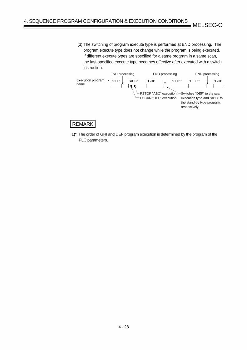
4 - 28
MELSEC-Q 4. SEQUENCE PROGRAM CONFIGURATION & EXECUTION CONDITIONS
(d) The switching of program execute type is performed at END processing. The
program execute type does not change while the program is being executed.
If different execute types are specified for a same program in a same scan,
the last-specified execute type becomes effective after executed with a switch
instruction.
Execution program name
END processing
"ABC" "GHI" "GHI" "DEF" "GHI"
END processing END processing
PSTOP "ABC" executionPSCAN "DEF" execution
Switches "DEF" to the scan execution type and "ABC" to the stand-by type program, respectively.
"GHI" * *
REMARK
1)*: The order of GHI and DEF program execution is determined by the program of the
PLC parameters.

4 - 29
MELSEC-Q 4. SEQUENCE PROGRAM CONFIGURATION & EXECUTION CONDITIONS
(3) Precautions for creating stand-by type programs
(a) Because present value updating and contact ON/OFF switching occurs at the OUT T instruction, timers cannot be used in stand-by type programs.
(b) Gathering sub-routine programs into a single program
1) Create the sub-routine programs in order, beginning from step 0 of the
stand-by type program. An END instruction is required at the end of the
sub-routine program.
2) Because there are no restrictions regarding the creation sequence of
sub-routine programs, the pointer numbers need not be assigned in
ascending order when creating multiple sub-routine programs.
3) Use common pointers. *
Sub-routine programs with common pointers can be called from all
programs executed by the QCPU.
(If local pointers are used, execution of the stand-by type program's sub-
routine programs will be impossible.)
QCPU
Program memory / Standard ROM / Memory card
Program A
WriteMain routine
program
END
Program B (Stand-by type program)
Program A
Program B
Use a common pointer. *(This does not have to be created in order.)
P508
RET
RET
Y10
RET
Y11
Y12
P500
P501
Write
Common pointer
4) See 10.13.1 for execution of a sub-routine program that contains local
devices.
REMARK
*: Refer to Section 10.9 for details regarding common pointers and local pointers.

4 - 30
MELSEC-Q 4. SEQUENCE PROGRAM CONFIGURATION & EXECUTION CONDITIONS
(c) Gathering interrupt programs into a single program
1) Create the interrupt programs in order, beginning from step 0 of the
stand-by type program.
An END instruction is required at the end of the interrupt program.
2) Because there are no restrictions regarding the creation sequence of
interrupt programs, the pointer numbers need not be assigned in
ascending order when creating multiple interrupt programs.
END
Program B (Stand-by type program)
Interrupt pointer (This does not have to be created in order.)
I32
IRET
IRET
Y10
IRET
Y11
Y12
I0
I28
Interrupt program
QCPU
Program memory / Standard ROM / Memory card
Program A
WriteMain routine
program
Program A
Program B
Write
REMARK
See Section 10.10 for details regarding interrupt pointers.

4 - 31
MELSEC-Q 4. SEQUENCE PROGRAM CONFIGURATION & EXECUTION CONDITIONS
4.2.5 Fixed scan execution type program
(1) Definition of fixed scan execution type program
(a) This program is a program executed at specified intervals.
Without describing an interrupt point and IRET instruction, a fixed scan
execution can be performed for each file.
(b) The type of execution is set to "Fixed San" by the program setting of PLC
parameters.
(2) Execution of fixed scan execution type program
(a) When multiple fixed scan execution type programs are present, a fixedsan
execution type program executed for a specified time is executed.
When multiple fixed scan execution type programs have been executed for a
specified time at the same timing, these programs are executed in the
ascending order of numbers for the program setting of the PLC parameters.
(b) When fixed scan execution type programs and interrupt programs (I28 to I31)
have been executed for a specified time at the same timing, the priority of
execution is given to the interrupt programs.
(c) Execution during network refreshing
When the execution conditions of fixed scan execution type programs are
established during the network refreshing, the network refresh is suspended,
and interrupt programs are executed.
Accordingly, even if the "block assurance of cyclic data for each station" is
made by the MELSECNET/10H network system, the assurace will not be
given if a device set at a station to be refreshed is used in the interrupt
programs.*1
Interrupt factor
Fixed scan execution type program execution
Link refresh execution
10ms 10ms 10ms 10ms
Link refresh operation is suspended, and the interrupt program is executed.
Fig. 4.5 Execution of Fixed Scan Execution Type Programs during Network Refreshing
REMARK
*1: See the following manual regarding the block assurace of cyclic datafor each station.
• Q-capable MELSECNET/10H network system reference manual

4 - 32
MELSEC-Q 4. SEQUENCE PROGRAM CONFIGURATION & EXECUTION CONDITIONS
(d) Execution during END processing:
When the execution condition of fixed scan execution type programs are established during the wait time of END instruction while the constant scan is executed, the fixed scan execution type programs are executed.
(e) See Section 10.6.2 regarding the processing of the index resister that must be performed when the program is switched over from the scan execution type program/low speed execution type program to the fixed scan execution type program.
(3) Setting of fixed scan execution type program for high speed execution and
overhead time
When fixed scan execution type programs are executed, the processing below is performed. • Save and return of index resister • Save and return of file name of file resister in use If "High Speed Execution" is selected from the interrupt program/fixed scan execution type program in setting the PC system of PLC parameters, the processeing above will not be performed. As a result, the overhead time for the fixed scan execution type programs can be reduced.
(Overhead time s) CPU type
Not executed at high speed Executed at high speed
Q02CPU 380 230
Q02HCPU, Q06HCPU, Q12HCPU, Q25HCPU 165 100
(4) Cautions on programming
(a) A device turned ON by a PLS instruction of a fixed scan execution type program is kept turned ON until the same type of the fixed scan execution type program is executed again.
X0 OFF
ON
M0 OFF
ON
END 0 0 ENDEND0 END 0 0 END END 0
PLS M0X0
PLS M0X0
Switched OFF by PLS M0 instruction
Switched ON by PLS M0 instruction at X0 leading edge (OFF to ON)
Fixed scan execution type program execution
(b) During the execution of a fixed scan execution type program, interruption is prohibited (DI). Therefore, do not execute EI/DI instructions during the programming of the fixed scan execution type program.
(c) During the programming of a fixed scan execution type program, a timer cannot be used. Because the timer updates the current values and turns ON/OFF at the time of execution of OUT T instruction, if the timer is used during the programming of the fixed scan execution type program, the current values will be updated only when the fixed scan execution type program is executed, and normal measurement will be disabled.
(d) When a fixed scan execution type program is executed, an interruption must be allowed by an EI instruction of the initial execution type program/scan execution type program.

4 - 33
MELSEC-Q 4. SEQUENCE PROGRAM CONFIGURATION & EXECUTION CONDITIONS
4.3 Operation Processing
4.3.1 Initial processing
This is a preprocessing for sequence operation execution, and is performed only once
as shown in the table below.
When the initial processing is completed, the QCPU goes in the RUN/STOP switch
setting status. (See Section 4.4.)
QCPU status Initial processing item When the power
is turned on. When reset is
executed. When STOP
to RUN *1
The I/O module initialization
Boot from the standard ROM/memory card
Device initialization of the range not latched
(bit device: OFF, word device: 0)
Execution of self-diagnosis in the QCPU
Automatic allocation of the I/O number of
installed modules
Start of the MELSECNET/10H network
information setting and network communication *2
Setting of device initialization values
: executed, : not executed
REMARK
1)*1: When parameters or programs are changed in the STOP status, reset by the
RESET/L.CLR switch.
When the RUN/STOP switch is turned from STOP to RUN without the reset, RUN
LED flashes.
When the RUN/STOP switch is turned from RUN to STOP to RUN again, the
QCPU goes in the RUN status, and the "When STOP to RUN" status becomes
effective.
2)*2: This is executed when parameters or programs are changed in the STOP status.
(When parameters are changed, the QCPU uses the parameters after the
change.)
This is not executed when parameters or programs are changed in the other
status.
4.3.2 I/O refresh (I/O module refresh processing)
In I/O refresh, an input (X) is received from the input module/intelligent function
module, and output (Y) of the QCPU is produced to the output module/intelligent
function module.
The I/O refresh is executed before the sequence program operation starts.

4 - 34
MELSEC-Q 4. SEQUENCE PROGRAM CONFIGURATION & EXECUTION CONDITIONS
4.3.3 Automatic refresh of the intelligent function module
When automatic refresh of intelligent function modules is set, communication with the
intelligent function modules of the designated data is performed.
4.3.4 END processing
This is a post-processing to return the sequence program execution to step 0 after
completing the whole sequence program operation processing once.
(a) When a refresh request is made from the network module, refresh processing
is performed.
(b) When the trace point of the sampling trace is at every scan (after END
instruction execution), the set device status is stored in the sampling trace
area.
POINT
(1) When the constant scan function (refer to Section 7.2) is set, END processing
time result is stored for the interval after END processing to the next scan.
(2) When executing the low-speed execution type program, the low-speed END
processing starts after the all low-speed execution type programs are
completed.
Refer to Section 4.2.3 for details regarding of the low-speed execution type
program and low-speed END processing.

4 - 35
MELSEC-Q 4. SEQUENCE PROGRAM CONFIGURATION & EXECUTION CONDITIONS
4.4 RUN, STOP, PAUSE Operation Processing
The QCPU has three types of operation states; RUN, STOP and PAUSE states.
The QCPU operation processing is explained below:
(1) RUN Status Operation Processing
(a) RUN status is when the sequence program operation is performed from step
0 to END (FEND) instruction to step 0 repeatedly.
(b) When entering the RUN state, the output state saved at STOP by the
parameter output-mode setting during STOP to RUN.
(c) The processing time of switching from STOP to RUN until the beginning of
sequence program operation changes with system configurations, but usually
is 1 to 3 seconds.
However, this time may be longer depending on the conditions.
(2) STOP Status Operation Processing
(a) STOP status is when the sequence program operations are stopped with the
RUN/STOP key switch or remote STOP is performed. (Refer to Section 7.6.1
for details regarding of remote STOP function.)
(b) When entering the STOP state, save the output state and turn off all output.
The device memory other than output (Y) is maintained.
(3) PAUSE Status Operation Processing
(a) The PAUSE state is when the sequence program operations are paused by
remote PAUSE function while maintaining the output and device memory status.
(Refer to Section 7.6.2 for details regarding of remote PAUSE function.)
(4) QCPU Operation Processing with RUN/STOP Key Switch Operation
QCPU operation processing
RUN/STOP
key switch operation
Sequence program
operation processing External output
Device memory
(Y, M, L, S, T, C, D)
RUN to STOP
Executes up to the
END instruction and
stops.
OS saves the output state
and all output are off.
Maintains the status immediately
before the STOP state.
STOP to RUN Starts at step 0.
Determined by the output
mode of the PLC parameter
at STOP to RUN.
Starts executing the operation
from the status immediately
before the STOP state. When a
device initial value is designated,
however, the value is set. Local
devices are cleared.
POINT The QCPU performs the following in any of RUN, STOP, and Pause status: • I/O module refresh processing • Data communication with the GPPW and serial communication module • Network refresh processing Therefore monitoring and/or test operation of I/O by the GPPW, read/write from the serial communication and communications with other stations by MELSECNET/10H can be performed in the STOP and Pause statuses.
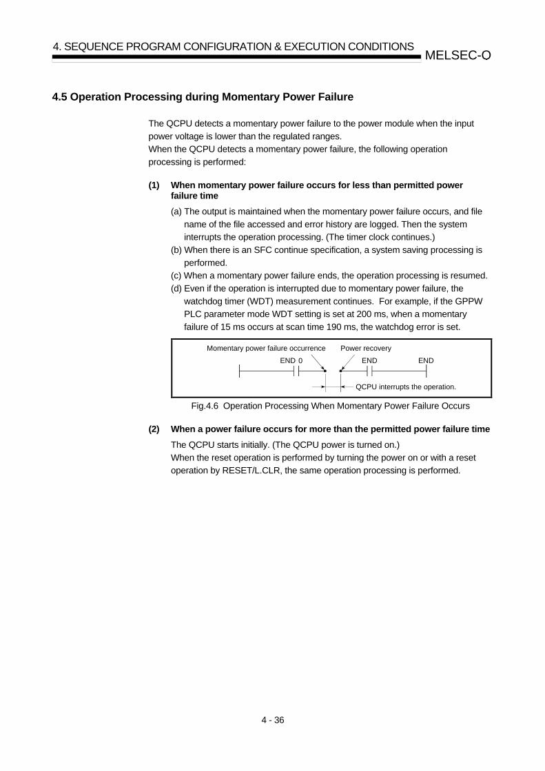
4 - 36
MELSEC-Q 4. SEQUENCE PROGRAM CONFIGURATION & EXECUTION CONDITIONS
4.5 Operation Processing during Momentary Power Failure
The QCPU detects a momentary power failure to the power module when the input
power voltage is lower than the regulated ranges.
When the QCPU detects a momentary power failure, the following operation
processing is performed:
(1) When momentary power failure occurs for less than permitted power
failure time
(a) The output is maintained when the momentary power failure occurs, and file
name of the file accessed and error history are logged. Then the system
interrupts the operation processing. (The timer clock continues.)
(b) When there is an SFC continue specification, a system saving processing is
performed.
(c) When a momentary power failure ends, the operation processing is resumed.
(d) Even if the operation is interrupted due to momentary power failure, the
watchdog timer (WDT) measurement continues. For example, if the GPPW
PLC parameter mode WDT setting is set at 200 ms, when a momentary
failure of 15 ms occurs at scan time 190 ms, the watchdog error is set.
QCPU interrupts the operation.
END
Power recoveryMomentary power failure occurrence
ENDEND 0
Fig.4.6 Operation Processing When Momentary Power Failure Occurs
(2) When a power failure occurs for more than the permitted power failure time
The QCPU starts initially. (The QCPU power is turned on.)
When the reset operation is performed by turning the power on or with a reset
operation by RESET/L.CLR, the same operation processing is performed.

4 - 37
MELSEC-Q 4. SEQUENCE PROGRAM CONFIGURATION & EXECUTION CONDITIONS
4.6 Data Clear Processing
(1) Data clear
The QCPU clears all data except for the following, when a reset operation is
performed with RESET/L.CLR switch, or power ON to OFF to ON.
1) Program memory data (except for when "clear program memory" is set at boot
specification.)
2) Data in the memory card
3) Device data with latch specification
4) File register data
5) Failure history data (when special relay SD storage)
Data in 3) and 5) are cleared using the RESET/L.CLR switch latch clear
operation or remote latch clear from the GPPW function.
Refer to Section 7.6.4 for details regarding of the remote latch clear.
(2) Device latch specification
(a) The method to specify device latch is to set the latch range for each device in
the device setting of the GPPW PLC parameter.
There are two types of latch range settings:
1) Valid latch clear key
Sets the latch range that can be cleared with the RESET/L.CLR switch
latch-clear operation.
2) Invalid latch clear key
Sets the latch range that can not be cleared even with the RESET/L.CLR
switch latch-clear operation.
(b) The devices that were set to invalid RESET/L.CLR switch can only be cleared
by an instruction or GPPW clear operation.
1) Instruction to clear method
Reset with the RST instruction or send K0 with the MOV instruction.
2) GPPW clear method
Clear all device memory in the online PLC memory clear (including
latch).
Refer to the GPP function software package operating manual for details
of the GPPW operation methods.
POINT
To clear file registers or local devices, use the RST instruction to perform a reset
operation, or use the MOV instruction to transmit KO.

4 - 38
MELSEC-Q 4. SEQUENCE PROGRAM CONFIGURATION & EXECUTION CONDITIONS
4.7 Input/Output Processing & Response Lag
The QCPU features a refresh type input/output processing format in which a batch communication with the input/output module occurs at END processing. A direct communication format is also possible by using direct access inputs/outputs at the sequence program to enable direct communication with the input/output module when the sequence program instructions are executed. For details regarding direct inputs and direct outputs, refer to Sections 10.2.1 and 10.2.2, respectively.
4.7.1 Refresh mode
(1) Definition of refresh mode
With the refresh mode, batch communication with the input/output modules occurs at END processing. (a) Batch reading of the input module ON/OFF information is executed in the
QCPU's internal input device memory when END processing occurs. This ON/OFF data (in the input device memory) is then used for processing which occurs when a sequence program is executed.
(b) The processing result of the output (Y) sequence program is output to the QCPU's internal output device memory, and batch output of the ON/OFF data (in output device memory) to the output module is executed when END processing occurs.
Input module
Output module
Peripheral device input area
For device memory output (Y)
CPU (operation processing area)
1)
2)
4)
5)
QCPU
Y20Y22
X0
At input refresh
At output refresh
3) Input (X) device memory
Area for communication with input module
*1
1) At input refresh
*2
• Input refresh:
Input information is read in a batch 1) from the input module at END processing, and
is stored in the input (X) device memory by an OR operation in the GPPW input area.
• Output refresh:
Data in the output (Y) device memory is output in a batch 2) to the output module at
END processing.
• When an input contact instruction has been executed:
Input information is read 3) from the input (X) device memory, and a sequence
program is executed.
• When an output contact instruction has been executed:
Output information is read 4) from the output (Y) device memory, and a sequence
program is executed.
• When an output OUT instruction has been executed:
The sequence program operation result 5) is stored in the output (Y) device memory.
Fig.4.7 Input/Output Information Flow at Refresh Mode

4 - 39
MELSEC-Q 4. SEQUENCE PROGRAM CONFIGURATION & EXECUTION CONDITIONS
REMARK
1)*1: The GPPW input area can be switched ON and OFF by the following:
• Test operation by the GPPW
• A network refresh by the MELSECNET/10H network system
• Writhing from a serial communication module
• CC-Link automatic refresh
2)*2: The output (Y) device memory can be switched ON and OFF by the following:
• Test operation by the GPPW
• A network refresh by the MELSECNET/10H network system
• Writhing from a serial communication module
• CC-Link automatic refresh

4 - 40
MELSEC-Q 4. SEQUENCE PROGRAM CONFIGURATION & EXECUTION CONDITIONS
(2) Response lag
Output response lags of up to 2 scans can result from input module changes.
(See Fig.4.8)
Ladder examples
Ladder for switching the Y5E outputON in response to an X5 input ON.
Y5EX5
55
Fastest possible Y5E ON
OFF
OFF
ON
ON
0
External contact
X5
OFF
ON
Y5E
OFF
ON
External load
END 0 56 END 0Input refresh Input refresh Output refresh
QCPUdevices
Lag time
(Minimum 1 scan)
The fastest possible Y5E ON occurs if the external contact is switched ON
immediately prior to the refresh operation. X5 then switches ON at the input refresh,
Y5E at step 56 switches ON, and the external load switches ON at the output refresh
following execution of the END instruction. In this case, the time lag between the
external contact ON and the external load ON is 1 scan.
Slowest possible Y5E ON
OFF
OFF
ON
ON
0
External contact
X5
OFF
ON
Y5E
OFF
ON
External load
END 0 56 END 0
Input refresh Input refresh Output refresh
QCPUdevices
Lag time
(Maximum 2 scan)
The slowest possible Y5E ON occurs if the external contact is switched ON
immediately prior to the refresh operation. X5 then switches ON at the input refresh,
Y5E at step 56 switches ON, and the external load switches ON at the output refresh
following execution of the END instruction. In this case, the time lag between the
external contact ON and the external load ON is 2 scan.
Fig.4.8 Output "Y" change in response to input "X" change

4 - 41
MELSEC-Q 4. SEQUENCE PROGRAM CONFIGURATION & EXECUTION CONDITIONS
4.7.2 Direct mode
(1) Definition of direct mode
In the direct mode the communication with the input/output modules is performed
when executing sequence program instructions.
With QCPU, direct mode I/O processing can be executed by using direct access
inputs (DX) and direct access outputs (DY).
See 10.2.1 for direct access inputs. See 10.2.2 for direct access outputs.
Input module
Output module
CPU (operation processing area)
DY25DY20
DX0
*1
*2
1)2)
3)
4)
5)
QCPU
Output (Y) devicememory
Peripheral device input areaInput (X)
device memory
• When an input contact instruction has been executed:
An OR operation is executed for the input module's input information 1) and the
GPPW input area's input information 2), and the result is stored in the input (X)
device memory. This data is then used as input information 3) at sequence
program execution.
• When an output contact instruction has been executed:
Output information 4) is read from the output (Y) device memory, and a sequence
program is executed.
• When an output OUT instruction has been executed:
The sequence program's operation result 5) is output to the output module, and is
stored in the output (Y) device memory.
Fig.4.9 Input/Output Information Flow at Direct Mode
REMARK
1)*1: The GPPW input area can be switched ON and OFF by the following:
• Test operation by the GPPW
• A network refresh by the MELSECNET/10H network system
• Writhing from a serial communication module
• CC-Link automatic refresh
2)*2: The output (Y) device memory can be switched ON and OFF by the following:
• Test operation by the GPPW
• A network refresh by the MELSECNET/10H network system
• Writhing from a serial communication module
• CC-Link automatic refresh

4 - 42
MELSEC-Q 4. SEQUENCE PROGRAM CONFIGURATION & EXECUTION CONDITIONS
(2) Response lag
Output response lags of up to 1 scans can result from input module changes.
(See Fig.4.10)
Ladder examples
Ladder for switching the DY5E outputON in response to an DX5 input ON.
DY5EDX5
55
Fastest possible DY5E ON
OFF
OFF
ON
ON
LD DX5OUT DY5E
0
DX5
DY5E
55 56
The fastest possible DY5E output ON occurs if the DX5 input is switched ON
immediately prior to the step 55 operation. If DX5 is ON when step 55's LD DX5 is
executed, DY5E will switch ON within that scan.
This condition represents the minimum time lag between the DX5 input ON and the
DY5E output ON.
Slowest possible DY5E ON
OFF
OFF
ON
ON
0
DX5
DY5E
END 0
Lag time
(Maximum of 1 scan)
OUT DY5E
LD DX5
55 56 55 56
The slowest possible DY5E output ON occurs if the DX5 input is switched ON
immediately after the step 55 operation. In this case, the DY5E output will switch ON
during the next scan.
This condition represents the maximum time lag (1 scan) between the DX5 input ON
and the DY5E output ON.
Fig.4.10 Output "Y" Change in Response to Input "X" Change

4 - 43
MELSEC-Q 4. SEQUENCE PROGRAM CONFIGURATION & EXECUTION CONDITIONS
4.8 Numeric Values which Can Be Used in Sequence Programs
Numeric and alphabetic data are expressed by "0" (OFF) and "1" (ON) numerals in the
QCPU.
This method of expression is called "binary code" (BIN).
The hexadecimal (HEX) expression method in which BIN data are expressed in 4-bit
units, and the BCD (binary coded decimal) expression method are also possible for the
QCPU.
The numeric expressions for the BIN, HEX, BCD, and Decimal (DEC) notations are
shown in Table 4.1 below.
Table 4.1 BIN, HEX, BCD, and Decimal Numeric Expressions
DEC (Decimal) HEX (Hexadecimal) BIN (Binary) BCD
(Binary Coded Decimal)
0 0 0 0
1 1 1 1
2 2 10 10
3 3 11 11
• • • •
• • • •
• • • •
9 9 1001 1001
10 A 1010 1 0000
11 B 1011 1 0001
12 C 1100 1 0010
13 D 1101 1 0011
14 E 1110 1 0100
15 F 1111 1 0101
16 10 1 0000 1 0110
17 11 1 0001 1 0111
• • • •
• • • •
• • • •
47 2F 10 1111 100 0111
• •
• •
• •
32766 7FFE 0111 1111 1111 1110 ——
32767 7FFF 0111 1111 1111 1111 ——
-32768 8000 1000 0000 0000 0000 1000 0000 0000 0000
-32767 8001 1000 0000 0000 0001 1000 0000 0000 0001
• •
• •
• •
-2 FFFE 1111 1111 1111 1110 ——
-1 FFFF 1111 1111 1111 1111 ——
Real numbers may also be used. (See Section 4.8.4)

4 - 44
MELSEC-Q 4. SEQUENCE PROGRAM CONFIGURATION & EXECUTION CONDITIONS
(1) External numeric inputs to QCPU
When designating numeric settings for the QCPU from an external source (digital
switch, etc.), a BCD (binary coded decimal) setting can be designated which is
the same as a decimal setting.
However, because the QCPU operation is based on BIN, if the QCPU uses
values designated in the BCD method as they are, it handles the values as BIN.
The QCPU operation based on such values will be different from the operation
specified by the designated values.
A BIN instruction is therefore provided for the QCPU to convert BCD input data to
the BIN data which is used by the QCPU.
A program which converts numeric data to BIN data can be created at the
sequence program in order to allow numeric settings to be designated from an
external source without regard to the corresponding BIN values.
BINP K4X0 D0
BCD D5 K4Y30
Digital switch
[Numeric data designation]
BCD input
BIN data
QCPU
XF X0
1234
Fig.4.11 Digital Switch Data Input to QCPU
(2) External numeric outputs from QCPU
A digital display can be used to display numeric data which is output from the
QCPU.
However, because the QCPU uses BIN data, it cannot be displayed at the digital
display as is.
A BCD instruction is therefore provided for the QCPU to convert the BIN data to
BCD data. A program which converts BIN data to BCD data can be created at
the sequence program in order to display the output data in a manner identical to
decimal data.
BINP K4X0 D0
BCD D5 K4Y30
QCPU
Digital display
[Numeric data designation]
Y3F Y30
BIN data
BCD output
Fig.4.12 Digital Display of Data from QCPU
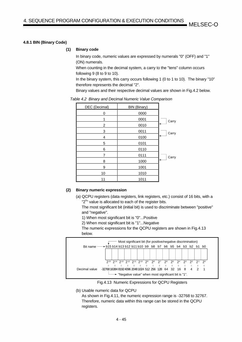
4 - 45
MELSEC-Q 4. SEQUENCE PROGRAM CONFIGURATION & EXECUTION CONDITIONS
4.8.1 BIN (Binary Code)
(1) Binary code
In binary code, numeric values are expressed by numerals "0" (OFF) and "1"
(ON) numerals.
When counting in the decimal system, a carry to the "tens" column occurs
following 9 (8 to 9 to 10).
In the binary system, this carry occurs following 1 (0 to 1 to 10). The binary "10"
therefore represents the decimal "2".
Binary values and their respective decimal values are shown in Fig.4.2 below.
Table 4.2 Binary and Decimal Numeric Value Comparison
DEC (Decimal) BIN (Binary)
0 0000
1 0001
2 0010 Carry
3 0011
4 0100 Carry
5 0101
6 0110
7 0111
8 1000 Carry
9 1001
10 1010
11 1011
(2) Binary numeric expression
(a) QCPU registers (data registers, link registers, etc.) consist of 16 bits, with a "2n" value is allocated to each of the register bits. The most significant bit (initial bit) is used to discriminate between "positive" and "negative". 1) When most significant bit is "0"...Positive 2) When most significant bit is "1"...Negative The numeric expressions for the QCPU registers are shown in Fig.4.13 below.
b15
8192
Bit name
Decimal value
Most significant bit (for positive/negative discrimination)
"Negative value" when most significant bit is "1".
16384 4096 20481024 512 256 128 64 32 16 8 4 2 1-32768
215 2 14 213 2 12 211 210 29 28 27 26 25 24 23 22 2 1 20
b14 b13 b12 b11 b10 b9 b8 b7 b6 b5 b4 b3 b2 b1 b0
Fig.4.13 Numeric Expressions for QCPU Registers
(b) Usable numeric data for QCPU As shown in Fig.4.11, the numeric expression range is -32768 to 32767. Therefore, numeric data within this range can be stored in the QCPU registers.

4 - 46
MELSEC-Q 4. SEQUENCE PROGRAM CONFIGURATION & EXECUTION CONDITIONS
4.8.2 HEX (Hexadecimal)
(1) Hexadecimal notation
In the hexadecimal system, 4 bits of binary data are expressed by 1 digit.
4 bits of binary data can express 16 values (0 to 15).
In the hexadecimal system, values from 0 to 15 are expressed by 1 digit.
This is accomplished by using alphabetic characters following "9", with a carry
occurring after "F", as follows:
A comparison of binary, hexadecimal, and decimal numeric expressions is shown
in Table 4.3 below. Table 4.3 Comparison of BIN, HEX, and DEC Numeric Expressions
DEC (Decimal) HEX (Hexadecimal) BIN (Binary)
0 0 0
1 1 1
2 2 10
3 3 11
• • •
• • •
• • •
9 9 1001
10 A 1010
11 B 1011
12 C 1100
13 D 1101
14 E 1110
15 F 1111
16 10 1 0000 Carry
17 11 1 0001
• • •
• • •
• • •
47 2F 10 1111
(2) Hexadecimal numeric expression
QCPU registers (data registers, link registers, etc.) consist of 16 bits.
Therefore, as expressed in hexadecimal code, the numeric value range which
can be stored is 0 to FFFFH.

4 - 47
MELSEC-Q 4. SEQUENCE PROGRAM CONFIGURATION & EXECUTION CONDITIONS
4.8.3 BCD (Binary Coded Decimal)
(1) BCD notation
BCD numeric expressions are binary expressions with a carry format identical to
that of the decimal system.
As with the hexadecimal system, BCD expressions are the equivalent of 4 binary
bits, although the BCD system does not use the A to F alphabetic characters.
A comparison of binary, BCD, and decimal numeric expressions is shown in
Table 4.4 below.
Table 4.4 Comparison of BIN, BCD, and DEC Numeric Expressions
DEC (Decimal) HEX (Hexadecimal) BIN (Binary)
0 0 0
1 1 1
2 10 10
3 11 11
4 100 100
5 101 101
6 110 110
7 111 111
8 1000 1000
9 1001 1001
10 1010 1 0000 Carry
11 1011 1 0001
12 1100 1 0010
(2) BCD numeric expression
QCPU registers (data registers, link registers, etc.) consist of 16 bits.
Therefore, as expressed in BCD code, the range of numeric values to be stored
is 0 to 9999.

4 - 48
MELSEC-Q 4. SEQUENCE PROGRAM CONFIGURATION & EXECUTION CONDITIONS
4.8.4 Real numbers (floating decimal point data)
(1) Real numbers
Real numbers are single precision floating decimal point data.
(2) Internal expression of floating decimal point data
The QCPU's internal expression of received real number data is explained below.
Real number data is expressed as shown below, using 2 word devices.
1. [Mantissa] × 2 (characteristic)
The bit configuration used for internal expression of floating decimal point data is
shown and explained below.
b31 b30 b23 b22 b16 b15 b0
b0 to b22 Mantissa
b23 to b30Characteristic
b31Mantissa code
• Mantissa code: The mantissa code is expressed at b31 as follows. 0: Positive 1: Negative
• Characteristic: The "n" of "2n" is expressed in various ways at b23 to b30, depending on the b23 to b30 BIN value.
b23 to b30
n
FFH
Not used
FEH
127
FDH
126
00H
Not used
02H
-125
01H
-126
81H
2
80H
1
7FH
0
7EH
-1
• Mantissa: For a binary value of 1.XXXXXX..., the "XXXXXX" portion of the value is expressed at b0 to b22 (23 bits).
(3) Calculation examples
Calculation examples are shown below (the nnnnn "X" indicates an X-system
data expression). (a) Storing "10"
(10) (1010) (1.01000..... 2 )10 2
32
Mantissa code Positive to 0
Characteristic 3 to 82H to (10000010)2
Mantissa (010 00000 00000 00000 00000)2
The data expression will therefore be 41200000H, as shown below.
Code Characteristic Mantissa0 1 0 0 0 0 0 1 0 0 1 0 0 0 0 0 0 0 0 0 0 0 0 0 0 0 0 0 0 0 0 0
4 1 2 0 0 0 0 0

4 - 49
MELSEC-Q 4. SEQUENCE PROGRAM CONFIGURATION & EXECUTION CONDITIONS
(b) Storing "0.75"
(0.75) (0.11) (1.100.... 2 )10 2
-12
Mantissa code Positive to 0
Characteristic -1 to 7EH to (01111110)2
Mantissa (100 00000 00000 00000 00000)2
The data expression will therefore be 3F400000H, as shown below.
Code Characteristic Mantissa0 0 1 1 1 1 1 1 0 0 1 0 0 0 0 0 0 0 0 0 0 0 0 0 0 0 0 0 0 0 0 0
3 F 4 0 0 0 0 0
POINT
• The monitor function for GPPW permits monitoring the real number data of the
QCPU.
• For a "0" value, "0" will be indicated at all the b0 to b31 bits.
• To increase the speed of real number computing, turn off the "Perform internal
arithmetic operations in double precision" check box in the "Floating point
arithmetic processing" Section of the PLC System sheet in the PLC Parameter
dialog box.
To turn off "Perform internal arithmetic operations in double precision", uncheck the check box.
REMARK
At the binary system, the portion of the value following the decimal point is calculated as
follows: 0.1 1 0 1
This bit expresses 2-1 This bit expresses 2-2 This bit expresses 2-3 This bit expresses 2-4
(0.1101)2 = 2-1 + 2-2 + 2-4 = 0.5 + 0.25 + 0.125 = (0.875)10

4 - 50
MELSEC-Q 4. SEQUENCE PROGRAM CONFIGURATION & EXECUTION CONDITIONS
4.9 Character String Data
(1) Character String Data
The QCPU uses ASCII code data.
(2) ASCII code character strings
ASCII code character strings are shown in the Table below.
"00H" (NUL code) is used at the end of a character string.
0 0 0 0 0 0 0 0 1 1 1 1 1 1 1 1
0 0 0 0 1 1 1 1 0 0 0 0 1 1 1 1
0 0 1 1 0 0 1 1 0 0 1 1 0 0 1 1
0 1 0 1 0 1 0 1 0 1 0 1 0 1 0 1Column
Low
(Comma)
(Minus)
(Period)
Under
line
0 1 2 3 4 5 6 7 8 9 A B C D E Fb8 b7 b6 b5 b4 b3 b2 b1
0 0 0 0
0 0 0 1
0 0 1 0
0 0 1 1
0 1 0 0
0 1 0 0
0 1 1 0
0 1 1 1
1 0 0 0
1 0 0 1
1 0 1 0
1 0 1 1
1 1 0 0
1 1 0 1
1 1 1 0
1 1 1 1
0
1
2
3
4
5
6
7
8
9
A
B
C
D
E
F
NUL (SP) 0 @ P ` p
! 1 A Q a q
" 2 B R b r
# 3 C S c s
$ 4 D T d t
% 5 E U e u
& 6 F V f v
' 7 G W g w
( 8 H X h x
) 9 I Y i y
* : J Z j z
+ ; K [ k {
, < L l |
- = M ] m }
. > N ^ n
/ ? O _ o
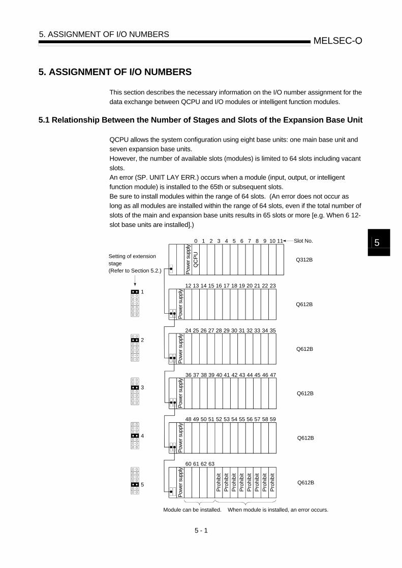
5 - 1
MELSEC-Q 5. ASSIGNMENT OF I/O NUMBERS
5
5. ASSIGNMENT OF I/O NUMBERS
This section describes the necessary information on the I/O number assignment for the
data exchange between QCPU and I/O modules or intelligent function modules.
5.1 Relationship Between the Number of Stages and Slots of the Expansion Base Unit
QCPU allows the system configuration using eight base units: one main base unit and
seven expansion base units.
However, the number of available slots (modules) is limited to 64 slots including vacant
slots.
An error (SP. UNIT LAY ERR.) occurs when a module (input, output, or intelligent
function module) is installed to the 65th or subsequent slots.
Be sure to install modules within the range of 64 slots. (An error does not occur as
long as all modules are installed within the range of 64 slots, even if the total number of
slots of the main and expansion base units results in 65 slots or more [e.g. When 6 12-
slot base units are installed].)
60 61 62 63
48 49 50 51 52 53 54 55 56 57 58 59
24 25 26 27 28 29 30 31 32 33 34 35
Setting of extension stage(Refer to Section 5.2.)
0 1 2 3 4 5 6 7 8 9 10 11 Slot No.
Pow
er s
uppl
y
Q312B
12 13 14 15 16 17 18 19 20 21 22 23
Q612B
Q612B
Q612B
Q612B
Q612B
1
2
3
4
5
36 37 38 39 40 41 42 43 44 45 46 47
Module can be installed. When module is installed, an error occurs.
QC
PU
Pow
er s
uppl
yP
ower
sup
ply
Pow
er s
uppl
yP
ower
sup
ply
Pow
er s
uppl
y
Pro
hibi
t
Pro
hibi
t
Pro
hibi
t
Pro
hibi
t
Pro
hibi
t
Pro
hibi
t
Pro
hibi
t
Pro
hibi
t

5 - 2
MELSEC-Q 5. ASSIGNMENT OF I/O NUMBERS
5.2 Installing Expansion Base Units and Setting the Number of Stages
There are two types of expansion base units: Q6 B for the installation of Q-series
modules and QA1S6 B for the installation of AnS-series modules.
(1) Connecting order of expansion base units
When using both Q6 B and QA1S6 B, connect all Q6 B modules closer to
the main base unit, then connect QA1S6 B modules.
(2) Setting order of the expansion stage numbers for expansion base units
Expansion base units require the setting of the expansion stage numbers (1 to 7)
using the stage setting connector.
Assign the expansion stage numbers starting from 1 to 7 to the expansion base
units counting from the one which is connected to the main base unit.
(3) Cautions to assign expansion stage numbers to expansion base units
(a) Assign consecutive numbers to expansion stages.
If you assign stage numbers to base units in "Auto" mode and assign some
stage numbers to no modules, "0" is assigned to the skipped stage as the
number of slots. Consequently, the number of vacant slots does not
increase. The I/O assignment also assigns "0" to the skipped stage as the
I/O points. (b) It is impossible to set and use the same expansion stage number with two or
more expansion base units. (c) You cannot use the system if two or more connector pins are inserted to the
stage setting connector.
On the contrary, you cannot use the system if no connector pin is inserted to
the stage setting connector.
16 17 18 19 20 21 22 23
Setting of extension stage
0 1 2 3 4 5 6 7
Q38B
8 9 10 11 12 13 14 15
Q68B
Q1S68B
Q1S68B
1
2
3
24 25 26 27 28 29 30 31
Main base unit
Extension base unit for module installation corresponding to the Q series (Q6 B is connected to the main base unit or Q6 B.)
Extension base unit for module installation corresponding to the AnS series (Q1S6 B is connected to the end of Q6 B or Q1S6 B.)
Stage setting connector
Pow
er s
uppl
yP
ower
sup
ply
Pow
er s
uppl
yP
ower
sup
ply
QC
PU

5 - 3
MELSEC-Q 5. ASSIGNMENT OF I/O NUMBERS
5.3 Base Unit Assignment (Base Mode)
There are "Auto" and "Detail" modes to assign the number of modules of the main and
expansion base units of QCPU.
(1) Auto mode
In Auto mode, the number of slots is assigned to the base units according to that
of the installed main and expansion base units.
The I/O numbers are assigned according to the modules which can be installed
to the current base unit.
(a) For 5-slot base unit: 5 slots are occupied
Q35B type main base unit0 1 2 3 4
Three slots are not occupied.
Pow
er s
uppl
y
QC
PU
(b) For 8-slot base unit: 8 slots are occupied
Q38B type main base unit0 1 2 3 4 5 6 7
Pow
er s
uppl
y
QC
PU
(c) For 12-slot base unit: 12 slots are occupied
Q312B type main base unit0 1 2 3 4 5 6 7 8 9 10 11
Pow
er s
uppl
y
QC
PU

5 - 4
MELSEC-Q 5. ASSIGNMENT OF I/O NUMBERS
(2) Detail mode
(a) In Detail mode, the number of slots is assigned to the individual base units
(main and expansion base units) by setting the I/O assignment of PLC
Parameter.
Use this mode to match the number of slots to the one for the AnS-series
base units (8 fixation).
(b) Cautions on setting the number of slots
The number of slots can be set regardless of the number of slots of the
module being used.
However, the followings result if the preset number of slots differs from that of
the installed base units.
1) When the designated number of slots is larger than that of the installed
base unit:
Among the designated slots, those after the slots occupied by the installed
base unit will be vacant slots.
Q35B type main base unit0 1 2 3 4
Three slots are occupied.
5 6 7
Vac
ant
Pow
er s
uppl
y
Vac
ant
Vac
ant
For example, when 8 slots are designated for a 5-slot base unit, 3 slots will
be vacant slots.The number of points for the vacant slots is the one
designated by PLC system of PLC Parameter or with I/O assignment.
(Default value is 16 points.)
2) When the designated number of slots is smaller than that of the base unit
being used:
The slots other than those designated are disabled.
For example, when 8 slots are designated for a 12-slot base unit, the 4
slots on the right of the base unit are disabled.
(If a module is installed to the disabled slot, an error [SP. UNIT LAY ERR.]
occurs.)
Q312B type main base unit0 1 2 3 4 5 6 7 8 9 10 11
When module is installed, an error occurs.
Module can be installed. (When eight slots are set)
Pro
hibi
tP
rohi
bit
Pro
hibi
t
Pro
hibi
t
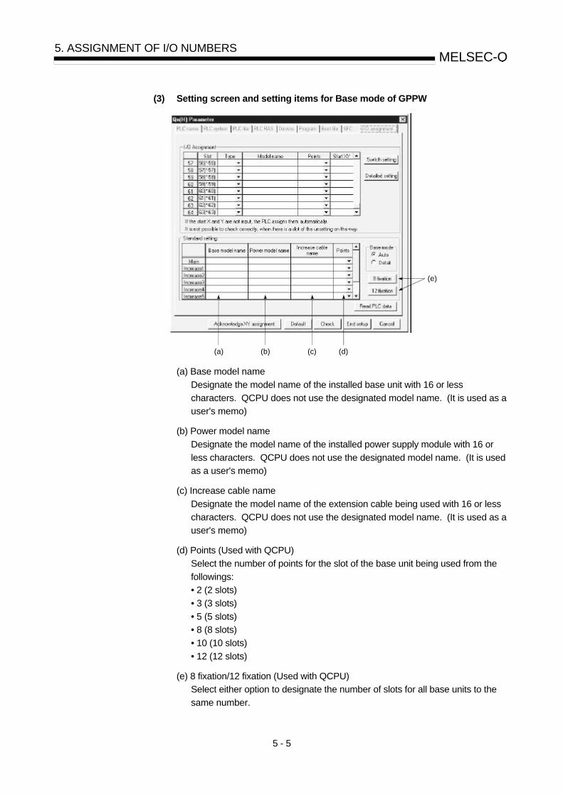
5 - 5
MELSEC-Q 5. ASSIGNMENT OF I/O NUMBERS
(3) Setting screen and setting items for Base mode of GPPW
(a) (b) (c) (d)
(e)
(a) Base model name
Designate the model name of the installed base unit with 16 or less
characters. QCPU does not use the designated model name. (It is used as a
user's memo)
(b) Power model name
Designate the model name of the installed power supply module with 16 or
less characters. QCPU does not use the designated model name. (It is used
as a user's memo)
(c) Increase cable name
Designate the model name of the extension cable being used with 16 or less
characters. QCPU does not use the designated model name. (It is used as a
user's memo)
(d) Points (Used with QCPU)
Select the number of points for the slot of the base unit being used from the
followings:
• 2 (2 slots)
• 3 (3 slots)
• 5 (5 slots)
• 8 (8 slots)
• 10 (10 slots)
• 12 (12 slots)
(e) 8 fixation/12 fixation (Used with QCPU)
Select either option to designate the number of slots for all base units to the
same number.
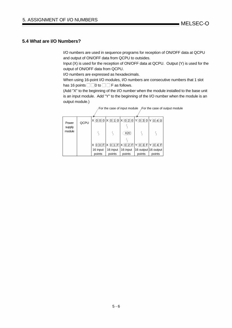
5 - 6
MELSEC-Q 5. ASSIGNMENT OF I/O NUMBERS
5.4 What are I/O Numbers?
I/O numbers are used in sequence programs for reception of ON/OFF data at QCPU
and output of ON/OFF data from QCPU to outsides.
Input (X) is used for the reception of ON/OFF data at QCPU. Output (Y) is used for the
output of ON/OFF data from QCPU.
I/O numbers are expressed as hexadecimals.
When using 16-point I/O modules, I/O numbers are consecutive numbers that 1 slot
has 16 points 0 to F as follows.
(Add "X" to the beginning of the I/O number when the module installed to the base unit
is an input module. Add "Y" to the beginning of the I/O number when the module is an
output module.)
QCPU
16 input points
X 0 0 0 X 0 1 0 X 0 2 0 Y 0 3 0 Y 0 4 0
X 0 0 F X 0 1 F X 0 2 F Y 0 3 F Y 0 4 F
For the case of input module For the case of output module
X2C
Power supply module
16 input points
16 input points
16 output points
16 output points

5 - 7
MELSEC-Q 5. ASSIGNMENT OF I/O NUMBERS
5.5 Concept of I/O Number Assignment
QCPU assigns I/O numbers at power-on or reset according to the following items.
As a result, you can control QCPU without using GPPW for I/O assignment.
To assign I/O numbers, follow the items below:
(1) Number of slots of base units
The number of slots of the main and expansion base units are set according to
the Base mode setting. (For Base mode, refer to Section 5.3.)
(a) In Auto mode, the number of slots is determined as the available number of
modules installed to each base unit.
For example, 5 slots are assigned for a 5-slot base unit, and 12 slots are
assigned for a 12-slot base unit.
(b) In Detail mode, the number of slots is determined as the one designated by
I/O assignment of PLC Parameter.
(2) Order of I/O number assignment
The I/O numbers are assigned to the modules from left to right consecutively,
starting from 0H assigned to the module on the right of the QCPU in the main
base unit.
(3) Order of I/O number assignment for expansion base units
The I/O numbers for expansion base units are assigned continuing from the last
number of the I/O number of the main base unit.
The I/O numbers for expansion base units are assigned to the units from left
(I/00) to right consecutively, in the order of the setting of the stage setting
connectors of the expansion base units.
(4) I/O numbers of each slot
Each slot of base units occupies the points of I/O numbers of the installed I/O
modules or intelligent function modules (special function modules).
When 32-point input module is installed on the right of QCPU, X0 to X1F are
assigned as I/O numbers.
(5) I/O numbers of vacant slots
If the base unit has vacant slots where no I/O modules or no intelligent function
modules (special function modules) are installed, the points designated by PLC
system setting of PLC Parameter are assigned to the vacant slots. (Default
value is 16 points.)
POINT
When the assignment for base units is conducted in Auto mode and no stage
number is assigned to a expansion base unit, "0" is assigned to both the number of
slots and the number of I/O points of the expansion base unit.
As a result, the number of vacant slots does not increase even when the expansion
stage of the expansion base unit is skipped.

5 - 8
MELSEC-Q 5. ASSIGNMENT OF I/O NUMBERS
The following shows the example of the I/O number assignment when the base unit is
set in Auto mode without I/O assignment:
Po
we
r su
pp
ly m
od
ule
0
X00
X0F
1 2 3 4
X10
X1F
X20
X3F
Y40
Y4F
Y50
Y8F
Q35B (5 slots occupied)
IN OUT
6
90
AF
7 8 95
B0
CF
D0
EF
YF0
YFF
100
10F
11
X110
X11F
12 13 14
Q68B (8 slots occupied)
10
X120
X12F
130
14F
150
16F
170
18F
15 16 17
Y190
Y19F
Y1A0
Y1AF
Y1B0
Y1BF
Extension cable
1
Slot No.
Allocate the I/O number with
the I/O points of each slot
I/O numbering direction
The slot numbers of the 1st stage's extension base unit continue from the last slot number of the main base unit.
Vacant slot points designated on the PLC system Setting screen under the parameter mode are allocated. (Default: 16 points)
The slot numbers of the 2nd stage's extension base unit continue from the last slot number of the 1st stage's extension base unit.
2
Q65B (5 slots occupied)
.........
.............
16 points
Input
module
Input
module
Input
module
Ou
tpu
t m
od
ule
Ou
tpu
t m
od
ule
16 points
32points
16 points
64 points
Po
we
r su
pp
ly m
od
ule
Inte
llig
en
t fu
nct
ion
mo
du
le
Inte
llig
en
t fu
nct
ion
mo
du
le
Inte
llig
en
t fu
nct
ion
mo
du
le
Ou
tpu
t m
od
ule
Va
can
t
32 points
32points
32points
16 points
16 points
IN OUT
Po
we
r su
pp
ly m
od
ule
Input
module
Input
module
Inte
llig
en
t fu
nct
ion
mo
du
le
Inte
llig
en
t fu
nct
ion
mo
du
le
Inte
llig
en
t fu
nct
ion
mo
du
le
Ou
tpu
t m
od
ule
Ou
tpu
t m
od
ule
Ou
tpu
t m
od
ule
16 points
16 points
32points
32points
32 points
16 points
16 points
16 points
QC
PU
POINT
The above example shows the case where the intelligent function module has 32
I/O points.
The number of I/O points may vary depending on the intelligent function module.
Refer to the manual of the intelligent function module being used and check the
number of the I/O points before assigning the I/O numbers.
5 - 9
MELSEC-Q 5. ASSIGNMENT OF I/O NUMBERS
5.6 I/O Assignment by GPPW
This section describes the I/O assignment using GPPW.
5.6.1 Purpose of I/O assignment by GPPW
I/O assignment by GPPW is used under the following circumstances.
(1) Reserving points when converting to module other than 16-point modules
You can reserve the number of points in advance so that you do not have to
change the I/O numbers when the current module will be changed to one with a
different number of I/O points in the future.
For example, you can assign a 32-point I/O module to the slot where a 16-point
I/O module is installed at present.
(2) Preventing I/O numbers from changing when converting modules
You can avoid the change in the I/O numbers when an I/O module other than 16-
point module or intelligent function module (special function module) is removed
due to a malfunction.
(3) Changing the I/O numbers to those used in the program
When the designed programs I/O numbers are different from the actual system
I/O numbers, each modules I/O numbers of base units can be set to program-I/O
numbers.
(4) Setting the response time of input modules (I/O response time)
To match the response time of the input modules to the system, select "Type" in
the I/O assignment beforehand. (For details, refer to Section 7.7.)
(5) Setting the switch of intelligent function modules
To set the switch of the intelligent function module, select "Type" in the I/O
assignment beforehand. (For details, refer to Section 7.8.)
(6) Setting outputs during QCPU error
To set the output status (retain/clear) of the output modules and intelligent
function modules when the QCPU stops the operation due to a stop error, select
"Type" in the I/O assignment beforehand.
(7) Setting QCPU operation during a hardware error of intelligent function
modules
To set the QCPU operation (continue/stop) during a hardware error of an
intelligent function module, select "Type" in the I/O assignment beforehand.
POINT
The I/O assignment is necessary for the switch setting of intelligent function
modules.

5 - 10
MELSEC-Q 5. ASSIGNMENT OF I/O NUMBERS
5.6.2 Concept of I/O assignment using GPPW
(1) I/O assignment for each slot
You can designate "Type" (module type), "Points" (number of I/O points), and
"Start XY" (head I/O number) individually for each slot of the base unit.
For example, to change the number of I/O points of the designated slot, you can
designate only the number of I/O points.
The items other than designated are set to the status where the base unit is
installed.
The I/O assignment is conducted according to the I/O assignment setting of PLC
Parameter.
(a) (b) (c) (d) (e)
(a) Slot
Displays the slot No. and the ordinal position of the slot in the base unit.
If the base unit is not designated in Detail mode, the stage number of the
base unit is shown as " * ", and the ordinal number of a slot is counted from
slot 0 of the main base unit.
(b) Type (Used with QCPU)
Select the type of module being installed from the followings:
• Vacant (Vacant slot)
• Input (Input module)
• Output (Output module)
• Intelligent (Intelligent function module or AnS-compatible special function module)
If the type is not designated, the type of the actually installed module is used.
(c) Model name
Designate the model name of the installed module with 16 or less characters.
QCPU does not use the designated model name. (It is used as a user's
memo)

5 - 11
MELSEC-Q 5. ASSIGNMENT OF I/O NUMBERS
(d) Points (Used with QCPU)
To change the number of I/O points of each slot, select it from the followings: • 0 (0 point) • 16 (16 points) • 32 (32 points) • 48 (48 points) • 64 (64 points) • 128 (128 points) • 256 (256 points) • 512 (512 points) • 1024 (1024 points) If the number of I/O points is not designated for a slot, the one of the actually installed module is used.
(e) Start XY (Used with QCPU) 1) When the I/O number of each slot is changed, you should designate the
head I/O number according to the change. If Start XY is not designated for a slot, the I/O number continuing from the last number of the currently designated slot is assigned.
2) Avoid the I/O number designation of each slot from overlapping the I/O numbers assigned by QCPU. An error (SP. UNIT LAY ERR.) occurs when the I/O numbers overlap.
(2) Slot status after I/O assignment
When the I/O number is assigned to a slot, the assigned I/O number takes
precedence regardless of the actual installation of a module. (a) If the designated number of I/O points is smaller than that of the actually
installed I/O module, some I/O points of the installed module are not used. For example, if a slot where a 32-point input module is installed is designated for a 16-point input module, the latter 16 points of the 32-point input module are disabled.
(b) If the designated number of I/O points is larger than that of the actually installed I/O module, the points exceeding the points of the actually installed module are set as dummies.
(c) Be sure to set the same module type for the installed module and the I/O assignment. If the module type of the I/O assignment is different from that of the actually installed module, a malfunction may result. For the intelligent function module, make sure that the numbers of I/O points are the same.
Actually installed module I/O assignment Result
Input module Output/vacant Vacant
Output module Input/vacant Vacant
Input module/output module Intelligent Error (SP. UNIT LAY ERR.)
Intelligent function module Input/output/vacant Error (SP. UNIT LAY ERR.)
Vacant slot Intelligent No error occurs.
(d) Be sure to assign the I/O numbers so that the last I/O number is within the
range of FFFH or less. An error (SP. UNIT LAY ERR.) occurs when the last
I/O number exceeds FFFH. (System monitor of GPPW shows "***" as an I/O
address.)

5 - 12
MELSEC-Q 5. ASSIGNMENT OF I/O NUMBERS
5.7 Examples of I/O Number Assignment
This section shows the examples of the I/O number assignment using GPPW.
(1) When changing the number of points of a vacant slot from 16 to 32 points:
Reserve 32 points to the slot position currently vacant (slot No. 3) so that the I/O
numbers do not change when a 32-point input module is installed in the future.
(The vacant slot for slot No. 12 is not changed from 16 points.) *1
(a) System configuration and I/O number assignment before the I/O assignment
with GPPW
0 1 2 3 4
Q38B
9 10 11 12
Q68B
8 13 14 15
F0
10F
110
12F
130
14F
150
16F
170
17F
Y180
Y19F
Y1A0
Y1BF
Y1C0
Y1DF
1
5 6 7
X00
X1F
X20
X3F
X40
X5F
60
6F
Y70
Y8F
Y90
YAF
YB0
YCF
YD0
YEF
Po
we
r su
pp
ly m
od
ule
Inp
ut
mo
du
le
Inp
ut
mo
du
le
Inp
ut
mo
du
le
Ou
tpu
t m
od
ule
Ou
tpu
t m
od
ule
Ou
tpu
t m
od
ule
Ou
tpu
t m
od
ule
Va
can
t
32points
32points
32points
16points
32 points
32 points
32 points
32 points
Po
we
r su
pp
ly m
od
ule
Inte
llig
en
t fu
nct
ion
mo
du
le
Inte
llig
en
t fu
nct
ion
mo
du
le
Inte
llig
en
t fu
nct
ion
mo
du
le
Ou
tpu
t m
od
ule
Va
can
t
Inte
llig
en
t fu
nct
ion
mo
du
le
Ou
tpu
t m
od
ule
Ou
tpu
t m
od
ule
32 points
32points
32points
32points
16 points
32 points
32 points
32 points
IN OUT
QC
PU
REMARK
*1: This is the case where the number of points for a vacant slot is set to 16 with
PLC system setting of PLC Parameter.

5 - 13
MELSEC-Q 5. ASSIGNMENT OF I/O NUMBERS
(b) I/O assignment with GPPW
Designate slot No. 3 to "32 points" on the I/O assignment screen of GPPW.
Select 32 points. (When the type is not selected, the type of the installed module will be selected.)
(C) I/O number assignment after the I/O assignment with GPPW
0 1 2 3 4
Q38B
9 10 11 12
Q68B
8 13 14 15
100
11F
120
13F
140
15F
160
17F
180
18F
Y190
Y1AF
Y1B0
Y1CF
Y1D0
Y1EF
1
5 6 7
X00
X1F
X20
X3F
X40
X5F
60
7F
Y80
Y9F
YA0
YBF
YC0
YDF
YE0
YFF
Po
we
r su
pp
ly m
od
ule
32points
Inp
ut
mo
du
le
Inp
ut
mo
du
le
Inp
ut
mo
du
le
Ou
tpu
t m
od
ule
Va
can
t
32points
32points
32points
32points
Ou
tpu
t m
od
ule
Ou
tpu
t m
od
ule
32points
32 points
Ou
tpu
t m
od
ule
32 points
IN OUT
Po
we
r su
pp
ly m
od
ule
Inte
llig
en
t fu
nct
ion
mo
du
le
Inte
llig
en
t fu
nct
ion
mo
du
le
Inte
llig
en
t fu
nct
ion
mo
du
le
Ou
tpu
t m
od
ule
Va
can
t
32 points
32points
32points
32 points
16points
Ou
tpu
t m
od
ule
Ou
tpu
t m
od
ule
Inte
llig
en
t fu
nct
ion
mo
du
le
32points
32points
32points
QC
PU

5 - 14
MELSEC-Q 5. ASSIGNMENT OF I/O NUMBERS
(2) Changing the I/O number of slots
Change the I/O number of a currently vacant slot (slot No. 3) to X200 through
X21F so that the I/O numbers of slot No. 4 and later slots do not change when a
32-point input module is installed to the currently vacant slot (slot No. 3).
(a) System configuration and I/O number assignment before the I/O assignment
with GPPW
0 1 2 3 4
Q38B
9 10 11 12
Q68B
8 13 14 15
F0
10F
110
12F
130
14F
150
16F
170
17F
Y180
Y19F
Y1A0
Y1BF
Y1C0
Y1DF
1
5 6 7
X00
X1F
X20
X3F
X40
X5F
60
6F
Y70
Y8F
Y90
YAF
YB0
YCF
YD0
YEF
IN OUT
Po
we
r su
pp
ly m
od
ule
Inte
llig
en
t fu
nct
ion
mo
du
le
Inte
llig
en
t fu
nct
ion
mo
du
le
Inte
llig
en
t fu
nct
ion
mo
du
le
Va
can
t
32points
32points
32points
32points
16points
Po
we
r su
pp
ly m
od
ule
32 points
Inp
ut
mo
du
le
Inp
ut
mo
du
le
Inp
ut
mo
du
le
Ou
tpu
t m
od
ule
Ou
tpu
t m
od
ule
32 points
32points
16 points
32points
Ou
tpu
t m
od
ule
Ou
tpu
t m
od
ule
32points
32points
32points
Va
can
t
Ou
tpu
t m
od
ule
32points
Ou
tpu
t m
od
ule
32points
Ou
tpu
t m
od
ule
32 points
Inte
llig
en
t fu
nct
ion
mo
du
le
QC
PU

5 - 15
MELSEC-Q 5. ASSIGNMENT OF I/O NUMBERS
(b) I/O assignment with GPPW
Designate the head I/O number of slot No. 3 to "200" and that of slot No. 4 to
"70" on the I/O assignment screen of GPPW.
"200" is designated as the head I/O number.
"70" is designated as the head I/O number. (When the head I/O number is not designated, the I/O number following the 3rd slot will be assigned.)
(C) I/O number assignment after the I/O assignment with GPPW
0 1 2 3 4
Q38B
9 10 11 12
Q68B
8 13 14 15
F0
10F
110
12F
130
14F
150
16F
170
17F
Y180
Y19F
Y1A0
Y1BF
Y1C0
Y1DF
1
5 6 7
X00
X1F
X20
X3F
X40
X5F
X200
X21F
Y70
Y8F
Y90
YAF
YB0
YCF
YD0
YEF
Po
we
r su
pp
ly m
od
ule
32points
Inp
ut
mo
du
le
Inp
ut
mo
du
le
Inp
ut
mo
du
le
Ou
tpu
t m
od
ule
Ou
tpu
t m
od
ule
32points
32points
32 points
32points
Ou
tpu
t m
od
ule
Ou
tpu
t m
od
ule
32points
32 points
Inp
ut
mo
du
le
32points
IN OUT
Po
we
r su
pp
ly m
od
ule
Inte
llig
en
t fu
nct
ion
mo
du
le
Inte
llig
en
t fu
nct
ion
mo
du
le
Ou
tpu
t m
od
ule
Ou
tpu
t m
od
ule
Ou
tpu
t m
od
ule
32points
32 points
32points
32points
16points
32 points
32 points
32points
Inte
llig
en
t fu
nct
ion
mo
du
le
Inte
llig
en
t fu
nct
ion
mo
du
le
Va
can
t
QC
PU

5 - 16
MELSEC-Q 5. ASSIGNMENT OF I/O NUMBERS
5.8 Checking the I/O Numbers
System monitor of GPPW allows the check of the installed modules of QCPU and their
I/O numbers. (For system monitor, refer to Section 7.19.)
6 - 1
MELSEC-Q 6. QCPU FILES
6
6. QCPU FILES
(1) QCPU's file type
(a) The QCPU parameters, programs, comment data, etc. are assigned "file
names" and "extension", and are then stored in the following memories:
• Program memory
• Standard ROM
• Memory card
When reading and writing this data from the GPPW to the QCPU, files can be
specified by their types (parameter, program, comment, etc.) without regard
to their extension. (The GPPW automatically assigns the appropriate
extension for the file type which has been specified.)
(b) It is impossible to set and use the same expansion stage number with two or
more expansion base modules.
(2) QCPU file management
The use of different file and extension names permits multiple files to be stored in
the QCPU.
Because the QCPU can also process a given program as one file, programs
created can be managed individually according to their "designer", "process", or
"function" by using different program file names.
Moreover, program execution is possible for multiple programs stored at the
QCPU.
(See Chapter 4 for QCPU program execution details.)
(3) File written from GPPW
The QCPU stores files written from the GPPW in the memory (program
memory/standard ROM/memory card).

6 - 2
MELSEC-Q 6. QCPU FILES
(4) File details
A file name, file size, and writing date of the file which are set at the time of
creation by the GPPW will be appended to each file written in the QCPU.
When monitoring the files by the GPPW, the files are displayed as shown below.
(a) File name
1) The file name consists of the file name (max. 8 chars) and the extension (3 chars). A file name of any file written from the GPPW onto the QCPU will be displaced on-screen in uppercase characters. When naming a file by using a sequence program, type a file name in uppercase characters. An extension which corresponds to the file type designated when the file was written in the QCPU by the GPPW is automatically appended to the file name.
2) The following Windows-reserved words cannot be used for a file name. • COM1 to COM9 • LPT1 to LPT9
• AUX
• CON
• PRN
• NUL
• CLOCK$
(b) Date & time
The date & time when the file was written from the GPPW to the QCPU is
indicated.
The on-screen date and time indicate the GPPW-side date and time.
(c) Size
The file size when written from the GPPW to the QCPU is indicated in byte
units. (To view the latest QCPU data, click on the Update button.)
Files are stored in the QCPU program file and standard ROM in 4-byte units
(1 step), and at the memory card in 1-byte units.
When calculating a file's size, at least 64 bytes (136 bytes for programs) will
be added to all user created files other than file registers.

6 - 3
MELSEC-Q 6. QCPU FILES
6.1 About the QCPU's Memory
(1) User Memory
A user memory can be created within the memory of the QCPU by using the
GPPW/sequence program.
The QCPU has the following built-in memories:
• Program memory
• Standard RAM
• Standard ROM
A memory card can be installed on the QCPU to increase the size of a user
memory.
(a) Programs used for arithmetic operations of the QCPU are stored in the
program memory. Programs stored in the standard ROM or on a memory
card are booted (read) into the program memory for arithmetic operation. A
batch of parameters and programs stored in the program memory can be
copied to the standard ROM/memory card (Flash card).
(b) Parameters and programs are stored in the standard ROM. These data are
used for ROM operation of the QCPU.
(c) File register and local device data is stored in the standard RAM. The use of
file registers in the standard RAM will enable high-speed access as is the
case with data registers.
(d) Memory card
A memory card can be connected to a memory card interface of the QCPU.
This allows the read/write of data. The QCPU supports three types of
memory cards: SRAM card, Flash card, and ATA card. 1) The SRAM card allows the write/read of programs through a sequence
program in the following cases where: • File registers are used in excess of 32 k points. • Sampling trace data is stored. • SFC trace data is stored. • Failure history data is stored. The use of file registers allows the write/read of data at 505 k points in a sequence program.
2) The Flash card allows only the read through a sequence program. The Flash card is useful when data written by the QCPU is read through a sequence program but no change is made to the data. The use of file registers allows a sequence program to read a maximum of 1018 k points of data written by the QCPU.
3) The ATA card is used for PLC user data (general-purpose data). Access to PLC user data stored on the ATA card can be made in CSV format/binary format by using a file access instruction (e.g. FWRITE) in a sequence program.
6 - 4
MELSEC-Q 6. QCPU FILES
(2) Types of Data Stored in the QCPU Memory or on the Memory Card
The table below shows the type of data stored in a standard RAM/standard ROM
or on a memory card.
QCPU Built-In Memory
Card (RAM) Memory Card (ROM)
Data Name Program
Memory
Standard
RAM
Standard
ROM SRAM Card Flash Card ATA Card
Remarks
Parameter 1 data/drive
Intelligent parameter 1 data/drive
Program *1 *1 *1 *1
Device comment *2 *3
Device initial value
File register *5 *4
Local device 1 data/CPU unit
Debug data
SFC trace data
Failure history data
PC user data *6
: Needed, : Stored, : Not stored
REMARK
1) *1: To execute a program requires to boot the program memory.
2) *2: Data can be written by operating from the GPPW. Device comments cannot
be used in an instruction of a sequence program.
3) *3: The read from a sequence program requires several scans.
4) *4: A sequence program allows the read only. No data can be written through
access from a sequence program.
5) *5: A standard RAM hold a single file at a maximum of 32 K points.
6) *6: Data can be written or read with the following instructions:
• S.FREAD (allows the batch read from a specified file on a memory card)
• S.FWRITE (allows the batch write to a specified file on a memory card)
7) The table below shows file names and extensions of data files stored in the
QCPU or on a memory card. Data Name File name
Parameter PARAM.QPA
Inteli parameter IPARAM.QPA
Program ***.QPG
Device comment ***.QCD
Device initial value ***.QDI
File register ***.QDR
Local device ***.QDL
Debug data ***.QTD
SFC trace data ***.QTR
Failure history data ***QFD
PLC user data ***.***
The * portions can be named by the user.
6 - 5
MELSEC-Q 6. QCPU FILES
(3) Drive Number
(a) The QCPU uses drive numbers to control standard RAMs, standard ROMs,
and memory cards. The GPPW specifies a selected memory (standard RAM,
standard ROM or memory card) to execute the read/write of parameters and
program files from and to the QCPU. There is no need to specify the drive
number when using the GPPW.
(b) The table below shows the drive numbers used to specify a selected memory
(program memory, standard RAM, standard ROM or memory card) when
using a sequence program. The drive number must be used to specify a
selected memory when the read/write is made through access from a serial
communication module.
Memory Drive Number
Program memory 0
Standard RAM 3 QCPU built-in
Standard ROM 4
Memory card (RAM) SRAM card 1
Flash card 2 Memory card (ROM)
ATA card 2
(4) Memory Capacity and Formatting
The table below shows the size of a memory of the QCPU and whether to format
a memory.
Q02CPU Q02HCPU Q06HCPU Q12HCPU Q25HCPU Whether to Format
Standard RAM 64k bytes Required
(Use the GPPW).
Program memory 28 k steps
(128 k bytes)
28 k steps
(128 k bytes)
60 k steps
(240 k bytes)
124 k steps
(496 k bytes)
252 k steps
(1008 k bytes)
Required
(Use the GPPW).
Standard ROM 128 k bytes 128 k bytes 240 k bytes 496 k bytes 1008 k bytes Not required.
SRM card Q2MEM-1MBS: 1M bytes
Required.
(Use the GPPW or a
personal computer)
Flash card Q2MEM-2MBS: 2M bytes
Q2MEM-4MBS: 4M bytes Not required.
Memory
card
ATA card
Q2MEM-8MBS: 8M bytes
Q2MEM-16MBS: 16M bytes
Q2MEM-32MBS: 32M bytes
Required.
(Use the GPPW or a
personal computer)

6 - 6
MELSEC-Q 6. QCPU FILES
6.2 Program Memory
(1) What is the Program Memory?
(a) The QCPU's program memory is an internal RAM that stores programs
executed by the QCPU.
(b) The data storage in the program memory is backed up by QCPU's built-in
batteries (Q6BAT).
(c) Before the QCPU can be used for the first time, the program memory must be
formatted by the GPPW.
For details regarding the formatting procedure by the GPPW, refer to GPPW
manuals.
POINT
(1) Before the QCPU can be used for the first time, the program memory must be
formatted by the GPPW.
For details regarding the formatting procedure by the GPPW, refer to GPPW
manuals.
(2) Programs are stored in the program memories in 1k step units.
(2) Data Storage
Data on parameters and programs can be stored in the program memory. For
the types of data stored in the program memory, see Section 6.1.
(3) Format
(a) Formatting Choose "Online" "Format PLC memory" to open the Format PLC memory
dialog box. Select "Program memory" from the Target Memory list box.

6 - 7
MELSEC-Q 6. QCPU FILES
(b) Memory capacity after formatting
The memory capacity of the program memory after formatting is as follows.
Table 6.1 Memory capacity after formatting *1
Model Name Memory Capacity *2 Max. Number of Files Stored
Q02CPU 28k steps (114688 bytes) 28
Q02HCPU 28k steps (114688 bytes) 28
Q06HCPU 60k steps (245760 bytes) 60
Q12HCPU 124k steps (507904 bytes) 124
Q25HCPU 252k steps (1032192 bytes) 252
(c) Formatting precautions 1) Formatting of program memory
The QCPU program memory can only be used after being formatted by the GPPW. When formatting the program memory, designate whether or not a system area is to be allocated for user settings. (Up to 16k steps (in 1k-step units) can be allocated for the user setting system area.)
System area
User files
Parameters, programs etc.
0 to 15k steps(Unit of 1k step)
Memory capacity after formatting (See the (b).)
2) System area setting If RS-232C and USB interfaces are connected to the GPPW, the system area user setting data is used for registering monitor data from the GPPW connected to serial communication module. The allocation of space for system and user-defined areas will make it much easier to perform monitoring operation by operating from the GPPW connected to the serial communications module. Although the designation of a user setting area speeds up monitoring from the GPPW connected to serial communication module, it also reduces the amount of space available for user files.
REMARK
1) *1: This table shows an example in which 0 k step is allocated for a system area.
2) *2: In computing the memory capacity, 1 step is equal to 4 bites.

6 - 8
MELSEC-Q 6. QCPU FILES
6.3 About the Standard ROM
(1) What is the standard ROM?
(a) The standard ROM is used for the ROM operation of the QCPU.
(b) Programs stored in the standard ROM are used and booted (read) to the
program memory after the setting is made in the Boot File sheet of the PLC
Parameter dialog box.
(c) The standard ROM does not need formatting.
(d) Data can be written onto the standard ROM by using the online functions:
"Write to PLC (Flash ROM)" and "Write the program memory to ROM."
POINTS
(1) Before writing data onto a standard ROM, all previous data stored in the
standard ROM are erased. For this reason, to write data onto the standard
ROM, you must first read and copy all previous data stored in the standard
ROM before writing necessary data therein. Please note that an error may
occur if data stored in the standard ROM is used in a sequence program, with
data being written in the standard ROM.
(2) For details regarding the formatting procedure by the GPPW, refer to GPPW
manuals.
(3) Programs are stored in the standard ROM in units of 1k steps.
(2) Data Storage
A standard ROM holds files that contains parameters and programs.
(3) Memory Capacity
Table 6.2 shows the memory capacity of standard ROMs.
Table 6.2 Memory Capacity
Model Name Memory Capacity *2 Max. Number of Files Stored
Q02CPU 28k steps (114688 bytes) 28
Q02HCPU 28k steps (114688 bytes) 28
Q06HCPU 60k steps (245760 bytes) 60
Q12HCPU 124k steps (507904 bytes) 124
Q25HCPU 252k steps (1032192 bytes) 252
REMARK
In computing a memory capacity, 1 step is equal to 4 bytes.

6 - 9
MELSEC-Q 6. QCPU FILES
6.4 About the Standard RAM
(1) What is the standard RAM?
(a) The standard RAM is used when using file registers or local devices without a
memory card being installed on the QCPU.
(b) When using the QCPU for the first time, a standard RAM must be formatted
before use by operating from the GPPW. See the GPPW manual for a
GPPW format procedure.
(c) Data can be written onto the standard RAM by using the online function:
"Write to PLC."
(2) Stored Data
A standard RAM holds two files: file register file and local device file. Any other
files cannot be written onto a standard RAM.
(3) Format
(a) Formatting
To format a standard RAM, choose "Online" "Format PLC memory" and
then select "Standard RAM" in the "Target memory" list box. See Section 6.2
for the PLC Memory Format dialog box.
(b) Memory capacity after formatted
Table 6.3 shows the memory capacity of a "formatted" standard RAM.
Table 6.3 Memory Capacity
Number of Files Stored
CPU Type Number of Files Stored File Register
File
Local Device
File
Q02CPU 32k words (64k bytes) 1 1
Q02HCPU 32k words (64k bytes) 1 1
Q06HCPU 32k words (64k bytes) 1 1
Q12HCPU 32k words (64k bytes) 1 1
Q25HCPU 32k words (64k bytes) 1 1

6 - 10
MELSEC-Q 6. QCPU FILES
6.5 Memory Card
(1) Memory card
(a) A memory card is used to expand the size of an internal memory of the
QCPU.
(b) There are three types of memory cards for use in the QCPU: SRAM card,
Flash card, and ATA card.
POINTS
(1) Before the memory card can be used for the first time, the memory card must
be formatted by the GPPW.
For details regarding the formatting procedure by the GPPW, refer to GPPW
manuals.
(2) Before writing data onto a Flash card, all previous data stored on the Flash card
are erased. For this reason, to write data onto the Flash card, you must first
read and copy all previous data stored on the Flash card before writing
necessary data thereon. Please note that an error may occur if data stored on
the Flash card is used in a sequence program, with data being written on the
Flash card.
(3) Programs are stored in the memory card in 512 bytes (128 steps) step units.
(2) Stored Data
A memory card holds parameter and program data. See Section 6.1 for the
types of data stored in a memory card.
(3) Format
(a) Formatting
To format a memory card, choose "Online" "Format PLC memory" and
then select "Memory card (RAM)" or "Memory card (ROM) in the "Target
memory" list box. See Section 6.2 for the PLC Memory Format dialog box.
(b) Memory capacity after formatted
Table 6.4 shows the memory capacity of a "formatted" memory card.
Table 6.4 Memory Capacity
Memory Card Type Memory Capacity Number of Files Stored
Q2MEM-1MBS 1011.5k bytes 256
Q2MEM-2MBF 2032k bytes 288
Q2MEM-4MBF 4080k bytes 288
Q2MEM-8MBA 7972k bytes 512
Q2MEM-16MBA 15964k bytes 512
Q2MEM-32MBA 31918k bytes 512
(c) Precautions
For a formatted memory card, a "memory card information" area is
automatically created on the memory card. This means that available space
could be decreased by the size of the newly created "memory card
information area."

6 - 11
MELSEC-Q 6. QCPU FILES
6.6 Writing Data in the Standard ROM or on the Flash Card
The "write to PLC" function in the GPPW Online menu does not allow the user to write
files in a standard ROM or on a Flash card. For writing files in a standard ROM or on a
Flash card by operating from the GPPW, the GPPW Online menu provides two
functions: "Write the program memory to ROM" and "Write to PLC (Flash ROM)."
(1) Write the program memory to ROM
(a) The "Write the program memory to ROM" function allows a batch of files
stored in a program memory to be written in a standard ROM or on a Flash
card. This function is useful when debugging programs stored in the program
memory.
(b) When the "Write a memory to ROM" function is executed, all files stored in
the standard ROM or Flash card are erased before a batch of files stored in a
program memory are written. No files can be added to the standard ROM or
Flash card.
(c) The memory capacity of a standard ROM or Flash card is the same as that of
a program memory. A memory of a larger size than the memory capacity of a
program memory cannot be used.
(d) To execute the "Write the program memory to ROM" function, set the length
of GPPW's time-check to 60 seconds or longer. Shorter time-check may
cause a time-out on the GPPW side. To execute the "Write the program
memory to ROM" function via the CC-Link network by operating from a
GPPW at a local station, set the length of CC-Link's CPU monitoring time
(SW0A) to 60 seconds or longer. The default is 90 seconds. Use the default
value when making the setting.
(2) Write to PLC (Flash ROM)
(a) The "Write to PLC (Flash ROM)" function is useful when writing a batch of
files specified by the GPPW onto a standard ROM or Flash card.
(b) The "Write to PLC (Flash ROM)" function can fill all available space in a
standard ROM or Flash card. If a program that contains a small number of
steps is written on a Flash card, it will take long to fill the Flash card with
programs. When a RS-232C interface is installed at Q2MEM-4MBF, a baud
rate of 115.2k bps takes about 14 minutes. To write data on a Flash card,
increase a baud rate or use a USB interface. If the "Write to PLC (Flash
ROM)" function is executed from a local station, communication time will get
longer.
(c) To execute the "Write to PLC (Flash ROM)" function, set the length of
GPPW's time-check to 60 seconds or longer. Shorter time-check may cause
a time-out on the GPPW side. To execute the "Write to PLC (Flash ROM)"
function via the CC-Link network by operating from a GPPW at a local station,
set the length of CC-Link's CPU monitoring time (SW0A) to 60 seconds or
longer. The default is 90 seconds. Use the default value when making the
setting.

6 - 12
MELSEC-Q 6. QCPU FILES
(d) When the "Write to PLC (Flash ROM)" function is executed, all files stored in
the standard ROM or on the Flash card are erased before a batch of files
specified by the GPPW are written. No files can be added to the standard
ROM or Flash card. To add new files to old files, read all the old files from the
QCPU and write them again onto the QCPU.
(e) The "Write to PLC (Flash ROM)" function can be executed when the QCPU is
in the RUN status. When file registers of the Flash card is used in a
sequence program, execute the "Write to PLC (Flash ROM)" function after
the QCPU enters into the STOP status. If the "Write to PLC (Flash ROM)"
function is executed when the QCPU is in the RUN status, an error may occur
and the QCPU may stop running.
(f) While the "Write to PLC (Flash ROM)" function is executed, the read/write
cannot be made from other modules. This may cause a time out on the side
of other modules.

6 - 13
MELSEC-Q 6. QCPU FILES
6.7 Executing Standard ROM/Memory Card Programs (Boot Run)
(1) Executing QCPU programs
(a) The QCPU processes programs which are stored in the program memory.
The QCPU does not perform operation of programs stored in the standard
ROM or memory cards.
(b) To process programs stored in the standard ROM and memory card,
designate file names to be booted (read) to program memory by the GPPW
(by a boot file setting in a PLC parameter).
Programs with file names designated by the boot file setting are booted from
the standard ROM/memory card to program memory and processed when
the power is turned ON or the QCPU is reset.
(2) Preparation for Boot Run
Perform the following steps in preparation for boot run: (a) Create a program.
Create a program used for the boot run.
(b) Select a boot file. Select a boot file from the "Boot file" sheet of the PLC Parameter dialog box.
(c) Make the QCPU hardware setting.
Set QCPU Dip switches to specify a parameter-driven drive.
(d) Insert a memory card. Insert a memory card in a slot if you want to store parameters or programs on
the memory card during the boot run.
(e) Write parameters and programs. Write parameters on the parameter-driven drive. Write a program Into the
memory specified in the "Boot file" sheet of the PLC Parameter dialog box.
(f) Execute a program. Reset the QCPU with the RESET/L.CLR switch. After the boot run is
completed in the specified memory, the BOOT LED lights up.

6 - 14
MELSEC-Q 6. QCPU FILES
(3) Changing Program Files While the QCPU is in the Run Status.
(a) While the QCPU is in the RUN status, addition/change/deletion of program
files from the standard ROM or memory card to the program memory can be
made by using any of the following instructions in a sequence program.
• PLOAD
• PUNLAOD
• PSWAP
For details on the PLOAD, PUNLAOD and PSWAP instructions, see the
QCPU (Q Mode)/QnACPU Programming Manual (Common Instructions).
(b) Even if a program file is changed while the QCPU is in the RUN status, the
settings specified in the Program sheet of the PLC Parameter dialog box will
remain unchanged. When the QCPU is in the STOP status, the settings
made in the Program sheet of the PLC Parameter dialog box must be
adjusted to any changes (addition, change or deletion of program names)
made when the QCPU was in the RUN status.
If no adjustment is made in the Program sheet of the PLC Parameter dialog
box, an error may occur when the QCPU enters from the STOP status to the
RUN status.
(4) Precautions for Executing Programs in the Standard ROM/Memory Card
(a) For boot run, store parameters (PLC parameters) of the boot file setting in a
standard RAM or memory card. If parameters are stored in a program
memory and a parameter-drive drive is set to "Program Memory,." the boot
file setting made in the PLC Parameter dialog box is ignored. As a result, a
boot run is not performed when power is turned on or when the PLC is reset.
(b) If programs are written in the program memory during the RUN status while a
boot run is performed by using a memory card (RAM), any change made will
be reflected in programs stored on the memory card (RAM). For details on
the writing of programs during the RUN status, see Section 7.10.
(c) If programs are written in the program memory during the RUN status while a
boot run is performed by using a standard ROM/memory card (ROM), any
change made will not be reflected in programs stored in the standard ROM or
on the memory card (ROM).
(d) In the Boot File sheet of the PLC Parameter dialog box, set the maximum
number of boot files to the number of files stored in the program memory.
The number of boot files will be decreased by one in the following cases
where:
• A header is specified.
• A PLC parameter of a boot file setting is booted.

6 - 15
MELSEC-Q 6. QCPU FILES
6.8 Program File Configuration
(1) Program File Configuration
(a) Program files consist of a file header, an execution program, and allocate
memory for "Write during RUN".
(b) As shown below, the size of a program stored in the QCPU includes all the
above components. 1) File header: The file name, file size, and file creation data, etc., are stored
in this area. The file header size is fixed to 136 bytes (34 steps).
2) Execution program: The created program is stored in this area. 1 step is 4 bytes.
3) Allocate memory for "Write during RUN": This area is used when write during RUN that write during RUN increases the number of steps is executed at the GPPW. Default value is set to 500 steps (2000 bytes). The number of allocate memory for "Write during RUN" can be changed using the online write to PLC program. The number of allocate memory for "Write during RUN" can be redefined if the number of allocate memory is not sufficient for write during RUN. (See Section 7.10.1.)
(2) The size of the program displayed by GPPW
During programming at the GPPW, the program size (the total of the file header
size and the number of created program steps) is displayed as the number of
steps as shown below.
During programming, the size of the program created is displayed.
"Number of steps used" display
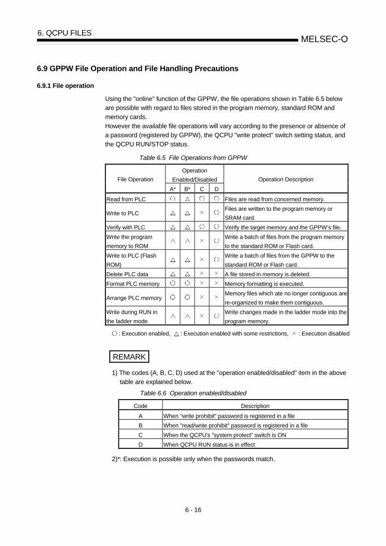
6 - 16
MELSEC-Q 6. QCPU FILES
6.9 GPPW File Operation and File Handling Precautions
6.9.1 File operation
Using the "online" function of the GPPW, the file operations shown in Table 6.5 below
are possible with regard to files stored in the program memory, standard ROM and
memory cards.
However the available file operations will vary according to the presence or absence of
a password (registered by GPPW), the QCPU "write protect" switch setting status, and
the QCPU RUN/STOP status.
Table 6.5 File Operations from GPPW
Operation
Enabled/Disabled File Operation
A* B* C D
Operation Description
Read from PLC Files are read from concerned memory.
Write to PLC Files are written to the program memory or
SRAM card.
Verify with PLC Verify the target memory and the GPPW's file.
Write the program
memory to ROM
Write a batch of files from the program memory
to the standard ROM or Flash card.
Write to PLC (Flash
ROM)
Write a batch of files from the GPPW to the
standard ROM or Flash card.
Delete PLC data A file stored in memory is deleted.
Format PLC memory Memory formatting is executed.
Arrange PLC memory Memory files which ate no longer contiguous are
re-organized to make them contiguous.
Write during RUN in
the ladder mode
Write changes made in the ladder mode into the
program memory.
: Execution enabled, : Execution enabled with some restrictions, : Execution disabled
REMARK
1) The codes (A, B, C, D) used at the "operation enabled/disabled" item in the above
table are explained below. Table 6.6 Operation enabled/disabled
Code Description
A When "write prohibit" password is registered in a file
B When "read/write prohibit" password is registered in a file
C When the QCPU's "system protect" switch is ON
D When QCPU RUN status is in effect
2)*: Execution is possible only when the passwords match.

6 - 17
MELSEC-Q 6. QCPU FILES
6.9.2 File handling precautions
(1) Power OFF (or reset) during program operation
(a) If power is switched OFF during a file operation which will not cause a file
shift, the memory data will not be lost.
(b) If the QCPU battery (Q6BAT) backup is in effect, the program memory data
will not be lost if the power is switched OFF during the following file
operations which cause a file shift.
• File size change
• Arrange PLC memory
• New file creation
• Writing a program file during the RUN status
• Writing a program in excess of allocate memory for 'Write during RUN'
• Reading a file with the PLOAD instruction
Files stored in the memory card will not be lost unless the memory card is
removed from the QCPU while the power is OFF.
POINT
(1) If the above operations are done, the data up to the power OFF will be stored in
the QCPU internal memory, and will be restored when power is switched ON
again. A battery backup is required in order to save internal memory data for
this reason.
(2) Simultaneous access of a single file from multiple GPPWs
The QCPU permits access to a single file from a single GPPW. When access to
the same file is made from multiple GPPWs, the file is accessible only when the
current processing is completed by the GPPW prior to the next processing.
REMARK
For details on the PLOAD instruction, see the QCPU (Q Mode)/QnACPU
Programming Manual (Common Instructions).

6 - 18
MELSEC-Q 6. QCPU FILES
6.9.3 File size
The file size differs with the types of files used. When a program memory, standard
RAM, standard ROM, and memory card are used, calculate the size of a file with
reference to the table 6.7 shown below.
Space for file storage is available as shown below:
• Program memory, standard ROM: 4096k bytes (1k steps)
• Memory card: 512 bytes
If a file is transferred from a memory card to a program memory during a boot run, the
size of available memory is changed after the file was transferred.
Table 6.7 List of File Size
Function Estimated File Size (in bytes)
Drive header 64
Parameter
Default: 293 (increased by the parameter setting)
For Reference:
Boot setting to 70 + (18 (Number of files) )
With the MELSECNET/10H setting to maximum 4096 / units increased
With ETHERNET setting to maximum 922 / units increased
With CC-LINK setting to maximum 251 / units increased
Sequence program 136 + (4 (Number of steps) )
Device comment
74 + (Total of comment data size of each device)
• Comment data size of a device = 10 + 10250 a + 40 b
• a: quotient of (Number of device points) / 256
• b: remainder of (Number of device points) / 256
Device init 66 + 44 n + 2 (Total number of device points specified in the device initial value setting)
• n : specified number of device initial values
File register 2 (Number of file register points)
Sampling trace data 362 + ( (20 + 2 (Number of word device points) + (Number of bit device pints) / 8 )
(Number of traces) + 12 (Device range)
Failure history data 72 + 54 (Number of failures stored)
SFC trace data Maximum 48k (in 1k units)
Local device
70 + 6 (Type of specified device) + 2 ( (total number of M and V points) / 16 + (D points) + 18
(Total points of T, ST and C) / 16)
• Symbols "M, V, D, T, ST, and C" stand for the following devices:
M: internal relay
V: edge relay
D: data register
T: timer
ST: relative timer
C: counter

7 - 1
MELSEC-Q 7. FUNCTION
7
7. FUNCTION
Function of QCPU module is as follows:
7.1 Function List
Functions of QCPU are listed below:
Item Description Reference
Constant scan Function to execute the program in a set time interval regardless of the program scan
time. Section 7.2
Latch function Function to maintain the device data when performing the reset operation during
power off. Section 7.3
Output status setting When
STOP to RUN
Function to set the output Y status (output before STOP/output after the calculation
execution) when the QCPU is set from STOP status to RUN status. Section 7.4
Clock function Function to execute the QCPU internal clock. Section 7.5
Remote operation Function to operate the QCPU from a remote place. Section 7.6
Remote RUN/STOP Function to stop and start operating the QCPU. Section 7.6.1
Remote PAUSE Function to temporarily stop the QCPU. Section 7.6.2
Remote RESET Function to reset the QCPU. Section 7.6.3
Remote latch clear Function to clear the QCPU latch data. Section 7.6.4
Relationship between
remote operation and
RUN/STOP status of QCPU
key switch
When performing remote operation, the relationship with RUN/STOP status of the
QCPU key switch setting is explained. Section 7.6.5
Change response time of the
QCPU-compatible input module
This function changes response time of the QCPU-compatible input module.
Response time is 1 ms, 5 ms, 10 ms, 20 ms, 70 ms. The default is 10 ms. Section 7.7
Set the switches of the QCPU-
compatible
This function sets up the QCPU-compatible intelligent-function module.
For setup procedures, see the manual of the intelligent function module. Section 7.8
Monitoring function This function monitors the status of programs and devices on the QCPU by operating
from the GPPW. Section 7.9
Write during RUN This function writes programs when the QCPU is in the RUN status. Section 7.10
Measure execution time This function displays the processing time of a program being executed, the number of
times to execute an interrupt program, and the execution time of a program. Section 7.11
Program list monitor This function displays the processing time of a program being executed. Section 7.11.1
Interrupt program monitor This function displays the number of times to execute an interrupt program. Section 7.11.2
Scan time measurement This function measures the execution time of a program between selected steps. Section 7.11.3
Sampling trace function This function samples specified device data from the QCPU at a specified timing. Section 7.12
Multiple-user debugging function This function enables multiple users to debug programs by using several GPPWs. Section 7.13
Watchdog timer This function monitors operational delays caused by QCPU's hardware and program
errors. Section 7.14
Self-Diagnosis function This function enables the QCPU to check for failures. Section 7.15
Failure history This function stores a failure history of diagnosis results in the memory. Section 7.16
Password registration This function provides read/write protection for files stored in the QCPU against access
from the GPPW. Section 7.17
System display This function connects to the GPPW and monitors system configuration. Section 7.18
LED display This function enables the front-mounted LEDs to indicate the operating conditions of
the QCPU. Section 7.19
LED display This function indicates the normal or abnormal operating conditions of the QCPU. Section 7.19.1
Preference setting This function sets failure preferences to turn off LED displays. Section 7.19.2

7 - 2
MELSEC-Q 7. FUNCTION
7.2 Constant Scan
What is Constant Scan?
The scan time differs because the processing time differs depending on whether
the instruction, which is used in the sequence program, is executed or not.
Constant scan is a function to execute the sequence program repeatedly while
maintaining the scan time at a constant time.
The I/O refresh is executed before the sequence program is executed. So the
I/O refresh stays constant even when the execution time of the sequence
program varies.
Scan time when constant scan is not used
END
5ms
Sequence program
0 END 0 END 0 END 0END processing
6ms 5ms
Scan time when constant scan setting is set to 7 ms
END
5ms
Sequence program
0 END 0
END processing
2msWait time
6ms
END 0
1ms 5ms
END 0
2ms
7ms7ms 7ms
Scan time when constant scan is set to 10 ms during multiple program execution
8ms
Sequence program C
END processing
2msWait time
10ms
Sequence program B
Sequence program A
9ms 1ms
10ms
Fig. 7.1 Constant scan operation
REMARK
When using a low-speed execution type program, the constant scan function setting
or low-speed execution type program execution time must be set.

7 - 3
MELSEC-Q 7. FUNCTION
(2) Setting the constant scan time
(a) The constant scan time setting is performed with the parameter mode PLC
RAS.
The constant scan setting range is 0.5 ms to 2000 ms.
A setting can be made in modules of 0.5 ms.
• When executing constant scan, set the constant scan time.
• When not executing a constant scan, leave the constant scan time blank.
[Example] When the constant scan is set to 10 ms.
(b) Set the set time of the constant scan larger than the maximum scan time of
the sequence program. Also, set the constant scan set time less than the
WDT set time.
(WDT Set Time) > (Constant Scan Set Time) > (Sequence Program maximum Scan Time)
If the sequence program scan time is larger than the constant scan set value,
the QCPU detects PRG.TIME OVER (an error code: 5010), the sequence
program is executed with the scan time by ignoring the constant scan.
0 1 2 3 4 1 2 3 4
0 0
1
END 0END
2 3 4 1 2 3 4
0END 0END
3.5ms 0.5ms
4ms 3.7ms
3.5ms0.2ms
3.4ms 0.6ms
4ms
Scan where the constant scan is not normal
Constant scan setting
Constant scan
Sequence program
5.3ms
5 ms
Fig. 7.2 Operation when the Scan Time is More than the Constant Scan
If the value is larger than the WDT set time, the QCPU detects a WDT error
and stops the program execution.

7 - 4
MELSEC-Q 7. FUNCTION
(c) The sequence program processing stops during the wait time from the last
END processing execution until the next scan starts. 1) If a low-speed execution type program is used, its execution will be
interrupted for -0.5 ms (a constant scan time setting). 2) If an interrupt error occurs after the END processing is executed, or a low-
speed execution type program exists, the interrupt program or low-speed
execution type program is executed.
(d) Constant Scan Time Difference
This section describes the precision of a constant scan time setting. 1) The remaining portion (wait time) of a constant scan time setting is 0.02 ms
on Q02CPU and 0.1 ms on Q02HCPU, Q06HCPU, Q12HCPU, Q25HCPU
when the following programs are not executed.
• low-speed execution type program
• interrupt program
• fixed scan execution type program 2) Wait time is 0.5 ms when a low-speed execution type program is used. If
the maximum processing time for one instruction in a low-speed execution
type program is 0.5 ms, the remaining portion of constant scan time is the
same as described in 1). If the maximum processing time exceeds 0.5 ms,
constant scan delays for an excessive duration. 3) Interrupt is enabled while an interrupt program/fixed scan execution type
program is executed. If constant scan time runs out when an interrupt
program/fixed scan execution type program is executed, constant scan
cannot be finished. When an interrupt program/fixed scan execution type
program is used, constant scan time could be shifted by the execution time
of an interrupt program/fixed scan execution type program.
REMARK
Refer to "QCPU (Q-mode)/QnACPU Programming Manual (Common Instructions)"
for the command processing time.

7 - 5
MELSEC-Q 7. FUNCTION
7.3 Latch Functions
(1) What is Latch Functions?
(a) The values of each QCPU device are set back to the default (bit device: OFF
and word device: 0) when;
• The QCPU power is turned on.
• The reset operation is performed.
• There is a momentary power failure for more than the permissible amount of
time.
Latch is a function to maintain the device details when the above conditions
occur.
The availability of latches does not affect the operation performed by a
program.
(b) The latch can be used to continue control by maintaining the production
quantity, defect count, and address even when there is a momentary power
failure for more than the permissible amount of time.
(c) The following devices can use the latch function:
(The default latch range is only the latch relay.) 1) Latch relay(L)
2) Link relay(B)
3) Annunciator(F)
4) Edge relay(V)
5) Timer(T)
6) Retentive timer(ST)
7) Counter(C)
8) Data register(D)
9) Link register(W)
(2) Latch Range Setting
The latch range setting is performed with the PLC parameter mode device
setting.
There is a range in which the latch clear key (RESET/L.CLR switch) becomes
valid or invalid in the latch range setting.

7 - 6
MELSEC-Q 7. FUNCTION
(3) Precautions
(a) Even if the device has specified the latch function, device will not retain the
latch if the local device is specified or the device initialization is specified.
(b) The device details of the latch range are maintained with the battery (Q6BAT)
attached to the CPU module. 1) A battery is necessary even if the sequence program is stored as a
standard ROM or a ROM in a memory card for usage.
2) The latch range device contents are destroyed when the battery connector
is disconnected from the CPU module connector when the CPU module
power is turned off.
(4) Clearing the Latch Range Device Data
(a) To clear the latch range device contents and set the default values, perform a
"latch clear". When latch clear is performed, the device details of devices in
the unlatched range will be cleared as well.
(b) For the device set in the parameter in a range where the latch clear key
becomes invalid, the device is not cleared even if a latch clear is performed.
If the "Latch (2): disable clear by latch clear key" option is selected, the
affected devices can be cleared with GPPW's Remote Latch Clear.
(See Section 7.6.4 for Remote Latch Clear.)
POINT
File registers (R) cannot be cleared with latch clear.
(See Section 10.7 for clearing file registers.)

7 - 7
MELSEC-Q 7. FUNCTION
7.4 Setting the Output (Y) Status when Changing from STOP Status to RUN Status
(1) Output (Y) Status when changing from STOP Status to RUN Status
When changing from RUN status to STOP status, the RUN status output (Y) is
stored in the sequence and all the outputs (Y) are turned OFF.
The QCPU prompts the user to produce or clear output status before STOP
status if the STOP status is switched to the RUN status. (By default, a program
will be executed after the output (Y) status before the STOP status has been
produced, with the STOP status switched to the RUN status.) (a) Previous State
After the output (Y) status before the STOP status is output, the sequence
program calculations are performed.
(b) Recalculate (Output is 1 Scan later)
Clears all output (Y) and outputs the output (Y) after executing the sequence
program calculations.
STOP status to RUN status
Replay output?
Output the output (Y) status right before changing to STOP status.
Execute the sequence program calculations
NO (Output after calculation execution)
YES (Replay output)
Clear the output (Y) status.
Fig. 7.3 Processing when Change from STOP Status to RUN Status

7 - 8
MELSEC-Q 7. FUNCTION
(2) Setting the Output (Y) Status when Changing from STOP Status to RUN
Status
The output (Y) status before the STOP status when switching from STOP status
to Run status can be set in the PLC System sheet of the PLC Parameter dialog
box.
(3) Precaution
If an output (Y) is forcefully turned ON with the QCPU in the STOP status, it will
not remain in the ON status even if the STOP status is switched to the RUN
status.
The output status is effected as specified in the PLC System sheet of the PLC
Parameter dialog box.

7 - 9
MELSEC-Q 7. FUNCTION
7.5 Clock Function
(1) What is Clock Function?
(a) The QCPU has a clock function in the CPU module.
Because the time data from the clock function can be read by the sequence
program, the time data can be used for time maintenance.
Also, the time data is used for time maintenance for the QCPU system
functions such as those for failure history.
The clock operations for the clock function are maintained even when the
PLC power is off or when there is a momentary power failure for more than
the permitted time, using the battery (Q6BAT).
(b) Clock Data
The time data is the year, month, day, hour, minute, second, and day of the
week data used for the QCPU clock element. There are the following:
Data Name Contents
Year Four digits in AD (Countable from 1980 to 2079)
Month 1 to 12
Day 1 to 31(Automatic leap year calculation)
Hour 0 to 23 (24 hours)
Minute 0 to 59
Second 0 to 59
0 Sunday
1 Monday
2 Tuesday
3 Wednesday
4 Thursday
5 Friday
Day of the week
6 Saturday
(2) Writing to and Reading from the Time Data Clock Element
(a) The following two methods can be used to write to the time data clock
element.
1) Method to write from GPPW
The time data is written in the clock element by displaying "Online" "Set
time" window.

7 - 10
MELSEC-Q 7. FUNCTION
2) Method to Write from the Program
The time data is written in the clock element by using the clock instruction
(DATEWR).
A program example to write the time data using the time data write
instruction (DATEWR).
MOVP D0X0
MOVP D1
MOVP D2
MOVP D3
MOVP D4
MOVP D5
MOVP D6
K1999
K8
K10
K11
K35
K24
K2
DATEWR D0
Year 1999
Month 8
Day 10
Hour 11
Minute 35
Second 24
Day Tuesday: 2
0
Write request
Refer to "QCPU (Q-mode)/QnACPU Programming Manual (Common
Instructions)" for details of the DATEWR instruction.
(b) Reading Time Data
When reading the time data to the data register, use the time data read
instruction (DATERD) from the program.
The figure below shows an example of a program used to read the clock data
with the DATERD instruction and then store it in D10 to D16.
DATERD D10X1
The time data is read in D10 to D16.*
Read request
Refer to the "QCPU (Q-mode)/QnACPU Programming Manual (Common
instructions) for the details of the DATERD instruction.
REMARK
1) Writing to and Reading from Time Data can be executed by special relays
(SM210 to SM213) and special registers (SD210 to SD213).
See Appendix 1 for details on special relay. See Appendix 2 for details on special
registers.
2) *: The figure below shows the clock data stored in D10 to D16. D10
D11
D12
D13
D14
D15
D16
4 digits in AD
Month
Date
Hour
Minute
Second
Day of the week
Refer to Section 7.5.1(1).
1999
8
10
11
35
24
2

7 - 11
MELSEC-Q 7. FUNCTION
(3) Precautions
(a) The time data is not written in the clock element at the beginning.
The QCPU system uses the clock data for failure history, etc. When using the
QCPU for the first time, you must first set the clock for accurate time and day.
(b) Even if a part of the time data is being corrected, all data must be written to
the clock again.
(c) When an invalid time data is written to the clock, normal clock operation
cannot be performed.
[Example]
Month 13 Day 32
(4) Precision
The precision of the clock function differs with the ambient temperature, as
shown below:
Ambient Temperature ( C) Accuracy (Day difference, S)
0 -3.18 to +5.25 (TYP.+2.12)
+25 -3.93 to +5.25 (TYP.+1.9)
+55 -14.69 to +3.53 (TYP.-3.67)
(5) About Year 2000 Problems
(a) Adjustment of Leap Years
The QCPU clock function allows the QCPU built-in clock element to
automatically correct a leap year of Year 2000. The user is not required to
make adjustments to the data and time setting of the clock element. The day
following February 28, 2000 is displayed February 29, 2000.
(b) Comparison of Clock Data
To compare QCPU's clock data with a sequence program, use the DATERD
instruction to read the clock data. The year data is read out in 4 digits. It can
be compared as it is by using a compare instruction.

7 - 12
MELSEC-Q 7. FUNCTION
7.6 Remote Operation
The QCPU provides the RUN/STOP switches for switching between the STOP status
and the RUN status. The RESET/L.CLR switch also provides the Reset and Latch
Clear functions.
The QCPU can allow control of the QCPU operation status from an external (GPPW
function, intelligent function module, and remote contact) source.
The following three options are available for remote operations:
• Remote RUN/STOP
• Remote PAUSE
• Remote LATCH CLEAR
REMARK
The serial communication module is used as the example to describe the intelligent
function module.
7.6.1 Remote RUN/STOP
(1) What is Remote RUN/STOP?
(a) The remote RUN/STOP performs RUN/STOP of the QCPU from an external
source with the QCPU RUN/STOP key switch at RUN.
(b) Using remote RUN/STOP for the following remote operations are useful:
1) When the QCPU is at a position out of reach
2) When performing RUN/STOP of the control board QCPU from an external
source
(c) Calculations during Remote RUN/STOP
The program calculation that performs remote RUN/STOP is as follows:
1) Remote STOP
Executes the program to the END instruction and enters the STOP state.
2) Remote RUN
When remote RUN is performed while in the STOP state using remote
STOP, the state changes to RUN and executes the program from step 0.
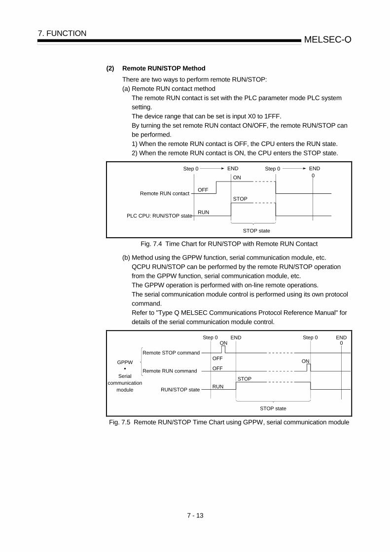
7 - 13
MELSEC-Q 7. FUNCTION
(2) Remote RUN/STOP Method
There are two ways to perform remote RUN/STOP:
(a) Remote RUN contact method
The remote RUN contact is set with the PLC parameter mode PLC system
setting.
The device range that can be set is input X0 to 1FFF.
By turning the set remote RUN contact ON/OFF, the remote RUN/STOP can
be performed.
1) When the remote RUN contact is OFF, the CPU enters the RUN state.
2) When the remote RUN contact is ON, the CPU enters the STOP state.
Remote RUN contactOFF
PLC CPU: RUN/STOP stateRUN
ON
STOP
Step 0 END Step 0 END0
STOP state
Fig. 7.4 Time Chart for RUN/STOP with Remote RUN Contact
(b) Method using the GPPW function, serial communication module, etc.
QCPU RUN/STOP can be performed by the remote RUN/STOP operation
from the GPPW function, serial communication module, etc.
The GPPW operation is performed with on-line remote operations.
The serial communication module control is performed using its own protocol
command.
Refer to "Type Q MELSEC Communications Protocol Reference Manual" for
details of the serial communication module control.
Remote STOP command
Step 0ON
END
OFF
Remote RUN command OFF
RUN/STOP stateRUN
STOP
Step 0
ON
END
STOP state
0
GPPW
Serial communication
module
Fig. 7.5 Remote RUN/STOP Time Chart using GPPW, serial communication module

7 - 14
MELSEC-Q 7. FUNCTION
(3) Precautions
(a) Take note of the following, because STOP has priority in QCPU:
1) The QCPU enters the STOP state when remote STOP is performed from
remote RUN contact, GPPW function, or serial communication module.
2) When QCPU is set to the STOP state with remote STOP, all external
factors which performed a remote STOP (remote RUN contact, remote
communication module, etc.) must be set to RUN.
REMARK
The RUN/STOP state is described below:
• RUN State .................State which repeatedly executes the calculations from step 0
to the END instruction in the sequence program.
• STOP State ...............State where the sequence program calculations are stopped
and the output (Y) is all OFF.

7 - 15
MELSEC-Q 7. FUNCTION
7.6.2 Remote PAUSE
(1) What is Remote PAUSE?
(a) Remote PAUSE performs the QCPU PAUSE function from an external
source, with the CPU RUN/STOP key switch at RUN position.
The PAUSE function stops the QCPU calculations while maintaining the
ON/OFF state of all output (Y).
(b) This can be used to maintain the output (Y) on even if the QCPU is changed
to the STOP state, in such areas as process control.
(2) Remote PAUSE Method
There are two ways to use remote PAUSE:
(a) Remote PAUSE Contact Method
The remote PUASE contact is set in the GPPW function parameter mode
PLC system setting.
The device range that can be set is input X0 to 1FFF.
1) The PAUSE state contact (SM204) is turned on when the END processing
is executed for the scan with both remote PAUSE contact and PAUSE
permission flag (SM206) on.
2) When the remote PAUSE contact is off or SM206 is turned off, the PAUSE
state is canceled, and the sequence program calculation is performed
again from step 0.
Remote PAUSE contact
OFF
ON
0 END
PAUSE state
0 END END 00 END
SM206OFF
ON
SM204OFF
ON
RUN/PAUSE state
RUN
ON when PAUSE condition met
PAUSE
Fig. 7.6 PAUSE Time Chart with Remote PAUSE Contact
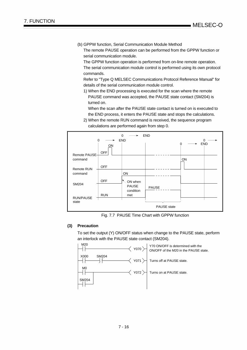
7 - 16
MELSEC-Q 7. FUNCTION
(b) GPPW function, Serial Communication Module Method
The remote PAUSE operation can be performed from the GPPW function or
serial communication module.
The GPPW function operation is performed from on-line remote operation.
The serial communication module control is performed using its own protocol
commands.
Refer to "Type Q MELSEC Communications Protocol Reference Manual" for
details of the serial communication module control.
1) When the END processing is executed for the scan where the remote
PAUSE command was accepted, the PAUSE state contact (SM204) is
turned on.
When the scan after the PAUSE state contact is turned on is executed to
the END process, it enters the PAUSE state and stops the calculations.
2) When the remote RUN command is received, the sequence program
calculations are performed again from step 0.
Remote PAUSE command
OFF
0 END
PAUSE state
0 END
0 END0
Remote RUN command
SM204OFF
ON
RUN/PAUSE state
RUN
ON when PAUSE condition met
PAUSE
ON
OFF
ON
Fig. 7.7 PAUSE Time Chart with GPPW function
(3) Precaution
To set the output (Y) ON/OFF status when change to the PAUSE state, perform
an interlock with the PAUSE state contact (SM204). M20
Y070
X000Y071
M0Y072
SM204
SM204
Y70 ON/OFF is determined with the ON/OFF of the M20 in the PAUSE state.
Turns off at PAUSE state.
Turns on at PAUSE state.
7 - 17
MELSEC-Q 7. FUNCTION
7.6.3 Remote RESET
(1) What is Remote RESET?
(a) The remote RESET resets the QCPU from an external source when the
QCPU is at STOP state.
Even if the QCPU RUN/STOP key switch is at RUN, the reset can be
performed when the QCPU is stopped and an error that can be detected by
the self-diagnosis function occurs.
(b) Remote RESET can reset the QCPU remotely when an error occurs for which
the QCPU cannot be operated directly.
In this case, perform a combination of remote RUN /STOP operations.
(2) Remote RESET Method
The remote RESET can only be performed from the GPPW function or serial
communication module operation.
To perform the remote RESET, follow the following steps:
(a) In the PLC System sheet of the PLC Parameter dialog box, turn on the
"Allow" check box in the "Remote reset" section, and then write parameters
onto the QCPU.
(b) Use the remote STOP to bring the QCPU to the STOP status.
(c) Reset QCPU with the remote RESET operation.
• For the GPPW function, this is performed in on-line remote operation.
• For the serial communication module, its own protocol command is used.
Refer to "Type Q MELSEC Communications Protocol Reference Manual" for
the details of the serial communication module control.
(3) Precautions
(a) To perform the remote RESET, turn on the "Allow" check box of the "Remote
reset" section in the PLC System sheet of the PLC Parameter dialog box, and
then write parameters onto the QCPU. If the "Allow" check box is not
checked, a remote RESET operation is not performed.
(b) Remote RESET cannot be performed when the QCPU is at the RUN state.
(c) After the reset operation is complete, the QCPU will enter into the RUN/STOP
key switch status.
1) With the RUN/STOP switch in the "STOP" position, the QCPU enters into
the "STOP" status.
2) With the RUN/STOP switch in the "RUN" position, the QCPU enters into
the "RUN" status.
POINT
If a remote RESET operation is performed while the QCPU is stopped due to error,
the QCPU will enter into the RUN/STOP switch status upon completion of the
reset.
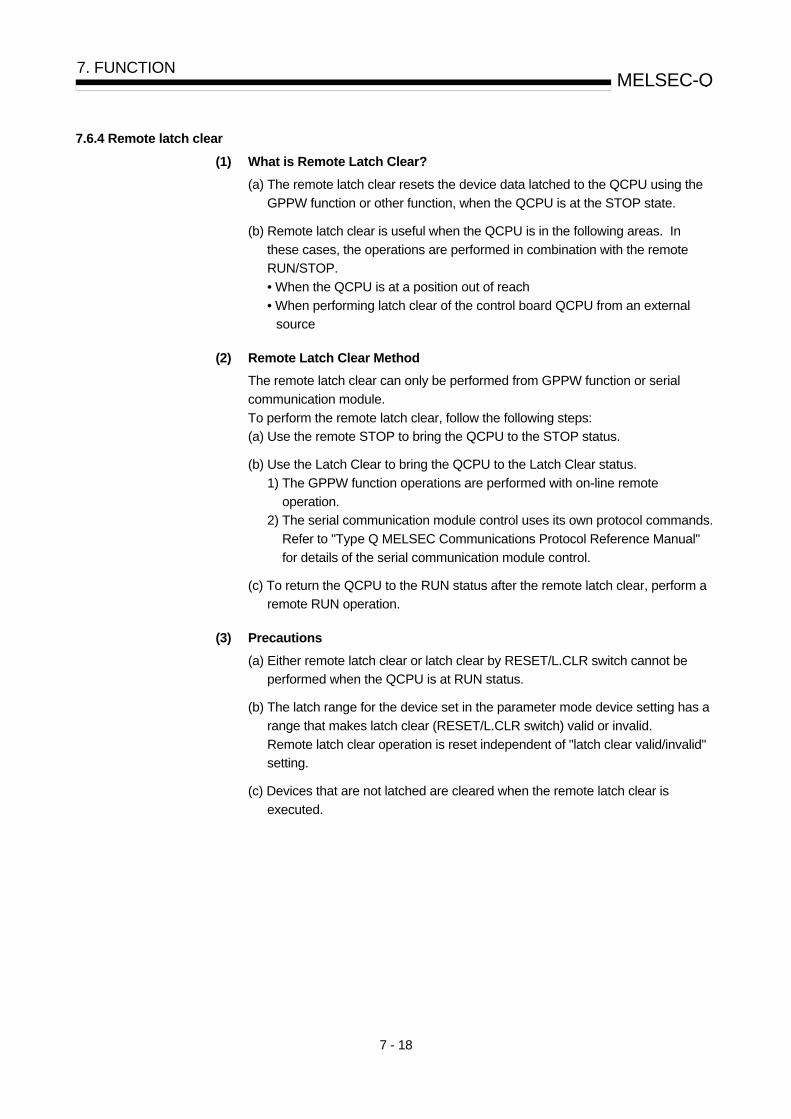
7 - 18
MELSEC-Q 7. FUNCTION
7.6.4 Remote latch clear
(1) What is Remote Latch Clear?
(a) The remote latch clear resets the device data latched to the QCPU using the
GPPW function or other function, when the QCPU is at the STOP state.
(b) Remote latch clear is useful when the QCPU is in the following areas. In
these cases, the operations are performed in combination with the remote
RUN/STOP.
• When the QCPU is at a position out of reach
• When performing latch clear of the control board QCPU from an external
source
(2) Remote Latch Clear Method
The remote latch clear can only be performed from GPPW function or serial
communication module.
To perform the remote latch clear, follow the following steps:
(a) Use the remote STOP to bring the QCPU to the STOP status.
(b) Use the Latch Clear to bring the QCPU to the Latch Clear status.
1) The GPPW function operations are performed with on-line remote
operation.
2) The serial communication module control uses its own protocol commands.
Refer to "Type Q MELSEC Communications Protocol Reference Manual"
for details of the serial communication module control.
(c) To return the QCPU to the RUN status after the remote latch clear, perform a
remote RUN operation.
(3) Precautions
(a) Either remote latch clear or latch clear by RESET/L.CLR switch cannot be
performed when the QCPU is at RUN status.
(b) The latch range for the device set in the parameter mode device setting has a
range that makes latch clear (RESET/L.CLR switch) valid or invalid.
Remote latch clear operation is reset independent of "latch clear valid/invalid"
setting.
(c) Devices that are not latched are cleared when the remote latch clear is
executed.
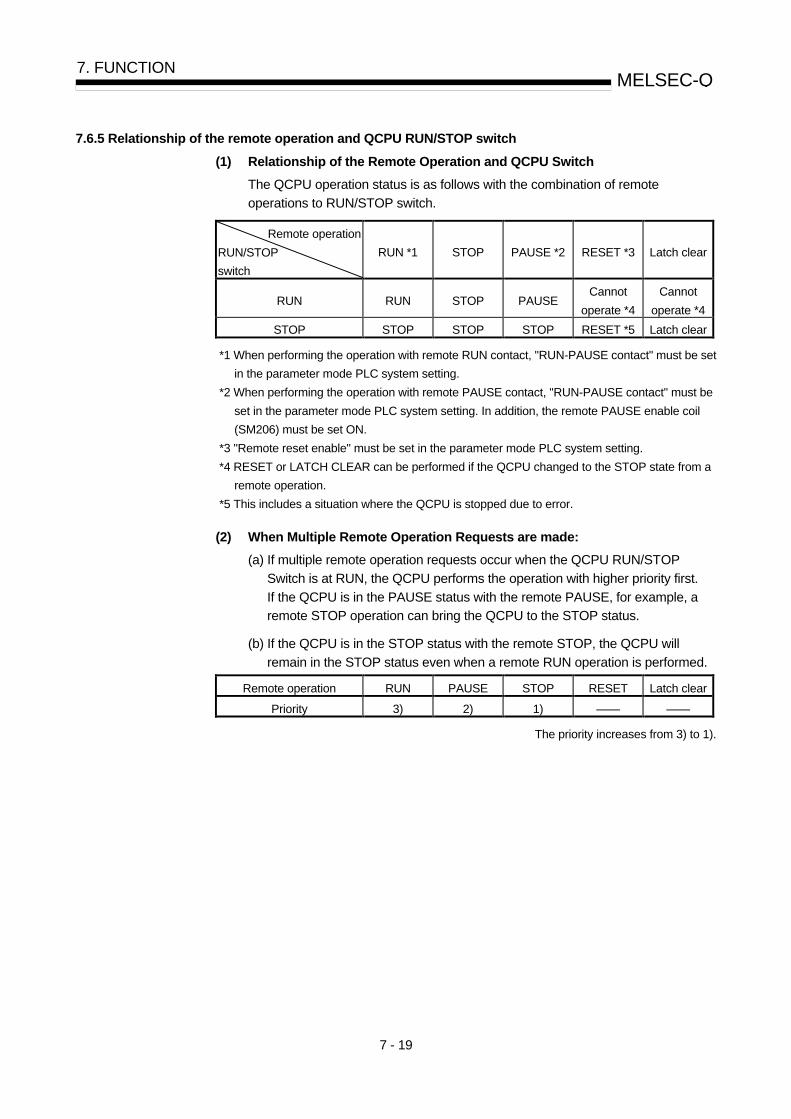
7 - 19
MELSEC-Q 7. FUNCTION
7.6.5 Relationship of the remote operation and QCPU RUN/STOP switch
(1) Relationship of the Remote Operation and QCPU Switch
The QCPU operation status is as follows with the combination of remote
operations to RUN/STOP switch.
Remote operation
RUN/STOP
switch
RUN *1 STOP PAUSE *2 RESET *3 Latch clear
RUN RUN STOP PAUSE Cannot
operate *4
Cannot
operate *4
STOP STOP STOP STOP RESET *5 Latch clear
*1 When performing the operation with remote RUN contact, "RUN-PAUSE contact" must be set
in the parameter mode PLC system setting.
*2 When performing the operation with remote PAUSE contact, "RUN-PAUSE contact" must be
set in the parameter mode PLC system setting. In addition, the remote PAUSE enable coil
(SM206) must be set ON.
*3 "Remote reset enable" must be set in the parameter mode PLC system setting.
*4 RESET or LATCH CLEAR can be performed if the QCPU changed to the STOP state from a
remote operation.
*5 This includes a situation where the QCPU is stopped due to error.
(2) When Multiple Remote Operation Requests are made:
(a) If multiple remote operation requests occur when the QCPU RUN/STOP
Switch is at RUN, the QCPU performs the operation with higher priority first.
If the QCPU is in the PAUSE status with the remote PAUSE, for example, a
remote STOP operation can bring the QCPU to the STOP status.
(b) If the QCPU is in the STOP status with the remote STOP, the QCPU will
remain in the STOP status even when a remote RUN operation is performed.
Remote operation RUN PAUSE STOP RESET Latch clear
Priority 3) 2) 1) —— ——
The priority increases from 3) to 1).
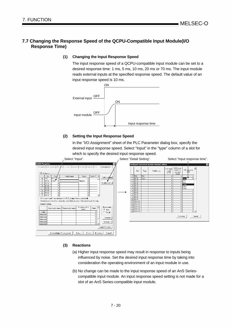
7 - 20
MELSEC-Q 7. FUNCTION
7.7 Changing the Response Speed of the QCPU-Compatible Input Module(I/O
Response Time)
(1) Changing the Input Response Speed
The input response speed of a QCPU-compatible input module can be set to a
desired response time: 1 ms, 5 ms, 10 ms, 20 ms or 70 ms. The input module
reads external inputs at the specified response speed. The default value of an
input response speed is 10 ms.
OFF
OFF
ON
ON
Input response time
External input
Input module
(2) Setting the Input Response Speed
In the "I/O Assignment" sheet of the PLC Parameter dialog box, specify the
desired input response speed. Select "Input" in the "type" column of a slot for
which to specify the desired input response speed. Select "Input". Select "Detail Setting". Select "Input response time".
(3) Reactions
(a) Higher input response speed may result in response to inputs being
influenced by noise. Set the desired input response time by taking into
consideration the operating environment of an input module in use.
(b) No change can be made to the input response speed of an AnS Series-
compatible input module. An input response speed setting is not made for a
slot of an AnS Series-compatible input module.
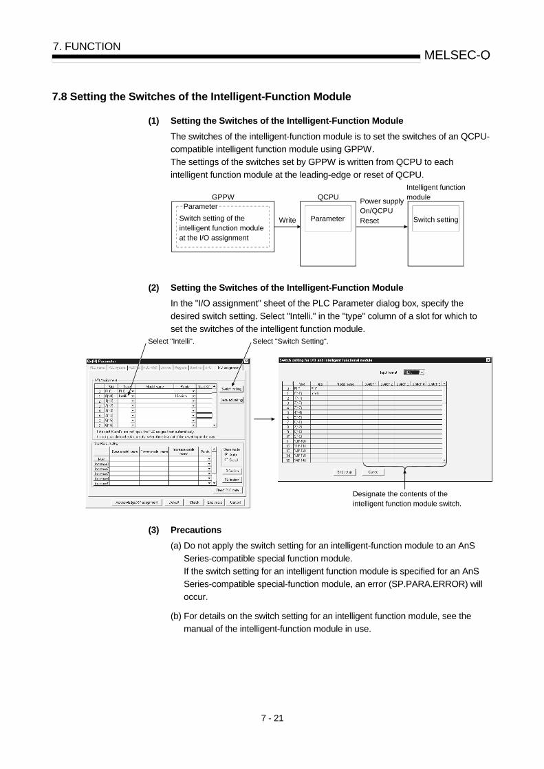
7 - 21
MELSEC-Q 7. FUNCTION
7.8 Setting the Switches of the Intelligent-Function Module
(1) Setting the Switches of the Intelligent-Function Module
The switches of the intelligent-function module is to set the switches of an QCPU-
compatible intelligent function module using GPPW.
The settings of the switches set by GPPW is written from QCPU to each
intelligent function module at the leading-edge or reset of QCPU.
Parameter
Switch setting of the intelligent function module at the I/O assignment
GPPW
Parameter Switch setting
QCPUIntelligent function module
Write
Power supply On/QCPU Reset
(2) Setting the Switches of the Intelligent-Function Module
In the "I/O assignment" sheet of the PLC Parameter dialog box, specify the
desired switch setting. Select "Intelli." in the "type" column of a slot for which to
set the switches of the intelligent function module. Select "Intelli". Select "Switch Setting".
Designate the contents of the intelligent function module switch.
(3) Precautions
(a) Do not apply the switch setting for an intelligent-function module to an AnS
Series-compatible special function module.
If the switch setting for an intelligent function module is specified for an AnS
Series-compatible special-function module, an error (SP.PARA.ERROR) will
occur.
(b) For details on the switch setting for an intelligent function module, see the
manual of the intelligent-function module in use.

7 - 22
MELSEC-Q 7. FUNCTION
7.9 Monitoring Function
(1) What is Monitoring Function?
(a) This is a function to read the program and device status of the QCPU through
the GPPW function peripheral device.
The QCPU performs the END processing to handle monitor requests from the
GPPW. The results of QCPU's END processing are displayed on the GPPW
side.
(b) Using GPPW set Monitoring conditions to monitor the QCPU operation status
in precise timings.
Also, by setting the monitoring stop condition, the precisely-timed monitoring
screen can be maintained.
(c) The use of local devices for execution of multiple programs makes it possible
to monitor local device data.
7.9.1 Monitor condition setting
(1) Setting monitor execution conditions when monitoring circuits.
Choose "Online" "Monitor" "Monitor condition" to open the Monitor
Condition dialog box. The following shows an example in which to start a
monitoring operation at the leading edge of Y70.
Select when monitoring by the contents of the device
Select when monitoring by Step No.
(a) When only Step no. is specified.
1) The monitor data sampling timing is when the status right before the
execution of the specified step becomes "Specify status".
2) The specification method for the execution status is indicated below:
a) When changing from non-execution state to executing state : <-P->
b) When changing from executing state to non-execution state : <-F->
c) Always when executing only : <ON>
d) Always when not executing only : <OFF>
e) Always regardless of status : <Always>
REMARK
When "Step no. [ 0]" is specified, set the condition to "Always".

7 - 23
MELSEC-Q 7. FUNCTION
POINT
If a step between the AND/OR blocks is specified as a monitor condition, monitor
data will be sampled after the pervious state of the specified step between the
blocks changes into a state of being specified by the LD instruction. The monitor
timing depends on the step specified as a monitor condition. The following shows
examples in monitoring when the 2nd step is ON.
(1) When the 2nd step is connected with the AND instruction:
As shown below, the monitor execution condition is established when both "X0"
and "X1" is ON.
0 Y20 X0 X1 X2
2nd step0 LD X01 AND X12 AND X23 OUT Y20
Circuit mode List mode
(2) When the 2nd step is connected between the AND/ON blocks:
As shown below, the monitor execution condition is established when "X1" is
ON. Whether "X" is ON or OFF does not affect the monitor execution condition.
0 Y20 X0 X1 X2
2nd step
X3
0 LD X01 LD X12 AND X23 OR X34 ANB5 OUT Y20
(b) When only "Device" is specified:
"Word Device" or "Bit Device" can be specified.
1) When "Word Device " is selected:
The monitor data sampling timing is when the current value of the specified
word device becomes the specified value.
Type a current value in decimal digits or hexadecimal digits.
2) When "Bit Device" is specified:
The monitor data sampling timing is when the execution status of the
specified bit device becomes the specified value.
Either the leading-edge or the fall can be specified for execution condition.
(c) When "Step no." and "Device" is selected:
The monitor data sampling timing is when the state right before execution of
the specified step and the execution state (present value) of the specified bit
device (word device) become the specified state.

7 - 24
MELSEC-Q 7. FUNCTION
POINT
When "Step no.[100]=< >, Word Device [D1]=[K5]" is specified as the detailed
condition in the following circuit, a monitor execution condition is established at the
leading edge of the 100th step where D1=5. X0 M0
Y20
INC D1
100th step
The monitor interval of the GPPW depends on the processing speed of the GPPW.
When a monitor condition is established during the monitor interval of the GPPW,
the monitor will be executed, even if a monitor condition is established at a shorter
interval than the monitor interval .
X0
D1 = 5
Monitor timing(QCPU)
100 100 100 100
M0
Step No.
(2) Monitor Stop Condition Set Up
Choose "Online" "Monitor" "Monitor stop condition" to open the Monitor
Stop Condition dialog box. The following shows an example in which to stop a
monitoring operation at the leading edge of Y71.
Select when monitor stop by the contentsof the device
Select when monitorstop by Step No.
(a) When "Step no." is specified:
1) The monitor stop timing is when the execution state of the step number
specified in the monitor condition becomes the specified state.
2) The specification method for the execution status is shown below:
a) When changing from non-execution state to executing state : <-P->
b) When changing from executing state to non-execution state : <-F->
c) Always when executing only : <ON>
d) Always when not executing only : <OFF>
e) Always regardless of status : <Always>
3) When "Step no." is not specified, the monitor stop timing is after the QCPU
END processing.

7 - 25
MELSEC-Q 7. FUNCTION
(b) When "Device" is specified:
"Word Device" or "Bit Device" can be specified.
1) When "Word Device " is selected:
The monitor stop timing is when the current value of the specified word
device becomes the specified value.
A current value can be expressed in decimal digits, hexadecimal digits, 16-
bit integral numbers, 32-bit integral numbers, or real numbers.
2) When "Bit Device" is specified:
The monitor stop timing is when the execution status of the specified bit
device becomes the specified value.
Either the leading-edge or the fall can be specified for execution condition.
(3) Precautions
(a) When monitoring after setting the monitor condition, the file displayed on the
GPPW is monitored. Match the file to be monitored by executing the "New
PLC Read" and file name on the GPPW.
(b) When monitoring the file register and the file register is not specified, 0 is
displayed.
(c) Perform the monitoring by matching the device allocation of the QCPU and
GPPW.
(d) When monitoring the buffer memory of the intelligent function module, the
scan time takes longer just like when executing the FROM/TO instruction.
(e) Multiple users can execute monitoring at the same time.
When multiple users are executing monitoring at the same time, take note of
the following:
• High speed monitoring can be performed by increasing 1k step in the
system area for every station's monitor file during formatting of internal
memory.
Up to 15 stations can be set as the station monitor file, but the program
space will be reduced.
• The detailed condition setting for the monitoring can only be set for one
user.
(f) The monitoring detailed condition setting can only be set in circuit monitor.
(g) When the same device is specified as the monitor condition and monitor stop
condition, specify "ON" or "OFF.
7 - 26
MELSEC-Q 7. FUNCTION
7.9.2 Monitoring test for local device
(1) Monitoring and Testing Local Devices
(a) Local devices specified in the Device sheet of the PLC Parameter dialog box
can be monitored or tested by operating from the GPPW. This function is
useful when debugging a program and monitoring local devices in a program
monitored by the GPPW. See Section 10.13.1 for local devices.
(b) Monitoring the Local Devices
The table below shows the status of three programs A, B, and C being
executed on the QCPU, with local devices D0 to D99 specified. It assumes
that these three programs are executed in the order of A B C (END
processing) A B ....
Monitor Device
D0 D100
When local devices are
specified
D0 in Program C is monitored. D100 is monitored after Program
C is executed.
When local devices are
not specified
D0 in the displayed program is
monitored.
D100 is monitored after the
displayed program is executed.
If the local device monitor setting is made and Program B is displayed, for
example, this makes it possible to monitor the local devices in Program B.
X0MOVP K2 D0
X1MOVP K3 D9
X10MOVP K4 D0
X11MOVP K8 D9
X20MOVP K3 D0
X21MOVP K6 D9
Program: A Program: B Program: C
Program execution ( "A" "B" "C" )
The local device data of the program "B" is displayed.
The local device monitor is set and the program "B" is monitored.
QCPU
7 - 27
MELSEC-Q 7. FUNCTION
(2) Monitoring the Local Devices
Monitor local devices in the following steps: Connect the peripheral device to the QCPU.
The local device of the displayed program is monitored.
Display the circuit with the circuit mode.
Select "Tool".
Select "Option". Display option window
Select "Program type". Change to the option selection window by program
Select "Monitor" to monitor the local device. Setting of the local device monitor
Change the mode to the monitor mode.
(3) Precautions
(a) It is only a single program that local devices can be monitored or tested by
operating from a single GPPW. Local devices in multiple programs cannot be
monitored or tested by operating from a single GPPW.
(b) It is a maximum of 16 programs that local devices can be monitored or tested
by operating from multiple GPPWs connected to a RS-232C serial
communication module of the QCPU.
(c) If local devices in a stand-by type program are monitored, scan time is
extended for some time because local device data is read and saved. See
Section 10.13.1 for details.
(d) Local devices in a fix scan execution type program cannot be monitored or
tested.

7 - 28
MELSEC-Q 7. FUNCTION
7.10 Writing in Program during QCPU RUN
When the QCPU is in the RUN status, you can write programs or files in any of the
following steps:
• Writing data in the circuit mode during the RUN status.
• Writing data by using pointers during the RUN status (see Section 7.13.2).
• Writing a batch of files during the RUN status.
7.10.1 Writing data in the circuit mode during the RUN status
(1) Writing data in the circuit mode during the RUN Status
(a) Writing data in the circuit mode during the RUN status is used to write a
program during the QCPU RUN status.
(b) Changing the program can be performed without stopping the process in
QCPU program using writing data in the circuit mode during the RUN status.
X0 X2
X1
Y30
X3 X4
X5
SET M10
END
GPPW
Change by GPPW and write in QCPU at the conversion.
(c) Writing to the program during RUN can be performed from a GPPW function
peripheral device connected to another station in the network.
GPPW
MELSECNET/10H
Change by GPPW and write in QCPU at the conversion.

7 - 29
MELSEC-Q 7. FUNCTION
(2) Precautions
Take a note of the following when writing during RUN:
(a) The memory that can be written during RUN is only program memory.
1) If the write during RUN is performed while booting a program from a
memory card (RAM), the program to be booted will be changed. While
booting, it takes some time until the write during RUN is completely
executed.
2) If the write during RUN is performed while booting a program from the
standard RAM or memory card (ROM), the program to be booted will not
be changed.
(b) A maximum of 512 steps can be written at once during RUN.
(c) When a low-speed execution type program is being executed, the RUN write
is started once the low-speed execution type program is complete. Also, the
low-speed execution is stopped temporarily during a RUN write.
Scan execution typeprogram step 0 to END
1 Scan1 Scan1 Scan1 Scan
Low-speed execution type program step 201 to 320
Low-speed execution type program step 321 to END
Low-speed execution type program step 0 to 120
Low-speed execution type program step 0 to 200
1) 2) 3) 4)
Scan execution typeprogram step 0 to END
Scan execution typeprogram step 0 to END
Scan execution typeprogram step 0 to END
1): RUN write command of the scan execution type program
2): RUN write execution of the scan execution type program
3): RUN write command of the low-speed execution type program
4): RUN write execution of the low-speed execution type program
(d) If the write during RUN is executed while the PLOAD, PUNLOAD or ASWP
instruction is executed, the processing will enter into a stand-by status for the
write during RUN. If the write during RUN is executed while the PLOAD,
PUNLOAD or ASWP instruction is executed, the execution of the instruction is
delayed until the write during RUN is executed. (e) The capacity of a QCPU's program file is a sum of the capacity of the
program created and steps used for the write during RUN. The write during
RUN is executed when the capacity of a program file is increased. If the
capacity of a program file becomes larger than what it was before, steps can
be assigned for the write during RUN. This means that the write during RUN
can be executed only when enough space is available in a user memory area.
If steps are assigned again while the write during RUN is executed, scan time
could be extended for a value shown below in the table. Controls are
interrupted for a value shown below in the table.
Step for Write During RUN CPU Type
If Not Changed If Assigned Again
QnCPU max. 0.963 ms max. 0.042 ms.
QnHCPU max. 30 ms max. 90 ms

7 - 30
MELSEC-Q 7. FUNCTION
7.10.2 Writing a batch of files during RUN
(1) File-Write During RUN function
(a) The file-write during RUN function is used to write a batch of files onto the
QCPU as shown below in the table.
QCPU Built-in Memory Card (RAM) Memory Card (ROM) Memory Name
Program Memory Standard RAM Standard ROM SRAM Card Flash Card ATA Card
Parameter
Intelligent parameter
Program
Device comment
Device initial value
File register
Local device
Debug data
SFC trace data
Failure history data
PLC user data
: Writable data , : Unwritable data
: Writable data for access from a sequence program
GPPW
Program file A
Writing of program file A
POINT
The file-write during RUN allows writing three types of files:
• Program: program memory, SRAM card, ATA card
• Device comment: program memory, SRAM card, ATA card
• File register: standard RAM, SRAM card
Any other files cannot be written while the QCPU is in the RUN status.

7 - 31
MELSEC-Q 7. FUNCTION
(2) Precautions
The precautions for file-write during RUN are as follows.
(a) The file-write during RUN can be executed when any of the following
conditions is met. A SFC program does not allow writing a batch of files
during the RUN status.
1) Program memory
• When continuous space is available.
• When space is available.
2) Memory card
• When space is available.
(b) Please note that scan time could be extended as shown below in the table if
the file-write during RUN is executed. Controls are stopped for some time as
specified by a value in the table.
Event QnCPU QnHCPU
When continuous space is available in a program memory (ms) max. 80 ms max. 300 ms
When space is available in a program memory (ms) max. 80 ms max. 300 ms
When space is available in a memory card (except ATA card) (ms) max. 120 ms max. 570 ms
Please note that scan tame is extended for 1.25 seconds at 30 k step when
an ATM card is in use.
(c) Please note that no access can be made from an instruction in a sequence
program while a batch of files is written, with the QCPU in the RUN status.
While the file-write during RUN is being executed, an instruction to make
access to a file is not executed.
(d) If a program file being executed is written when the QCPU is in the RUN
status, the following will not work properly. After the write is complete, a rise
instruction is executed only when its execution condition is OFF.
• LDF
• ANDF
• ORF
• MEF
• PLF

7 - 32
MELSEC-Q 7. FUNCTION
7.11 Execution Time Measurement
This is a function to display the processing time of the program being executed.
This is used to find out the effect of each program's processing time on the total scan
time.
There are three functions to the execution time measurement. The details of each
function are indicated in sections 7.11.1 to 7.11.3.
• Program monitor list
• Interrupt program monitor list
• Scan time measurement
7.11.1 Program monitor list
(1) What is Program Monitor List?
(a) This is a function to display the processing time of the program being
executed.
(b) The scan time, number of times executed, and processing time by item can
be displayed for each program.
(2) Using the Program Monitor List
(a) Choose "Online" "Monitor" "Program monitor list". The Program Monitor
List dialog box appears on screen.
(b) The scan time, number of times executed, and processing time by item can
be displayed for each program.
a)
c)
b)
7 - 33
MELSEC-Q 7. FUNCTION
a) "Total Scan Time"
The monitor time set in WDT(the watchdog timer) of "PLC RAS Setting" in
the parameter mode and total scan time for each program type are
displayed.
1) "Monitor Time"
The monitoring time for the scan execution type program, initialization
program, and low-speed execution type program are displayed.
If the scan time exceeds this time, the QCPU displays the watchdog
timer error.
2) "Sum of Scan Time"
The total time in each item stated in "Scan Time Details for Scan
Execution" are displayed.
"Constant" indicates the constant scan waiting time when the setting is
made for constant scan. b) "Scan Time Details for Scan Execution"
The details of the scan time are displayed.
1) "Program"
The total execution time of the scan execution type program is
displayed.
2) "END operation Time"
The END operation time is displayed.
3) "Low-Speed Execution Type Program"
This indicates the total execution time of a low-speed execution type
program when making the setting for the execution time of a low-speed
execution type program or constant scan time.
4) "Constant Waiting"
The constant scan stand by is displayed when setting the constant scan
time. However, when the low-speed execution type program execution
time is set as well, this value is 0.000 ms. c) "Each Program Execution Status"
The program execution status of the program specified in "Auxiliary
Setting" of the parameter mode is displayed.
1) "Program"
The program name is displayed in the order set in the parameter.
2) "Execute"
The program type set in the parameter is displayed.
3) "Scan Time"
The actual scan time (current value) is displayed. At the program stop
(wait) state, the scan time is displayed as 0.000 ms.
4) "Constant waiting"
The number of times the program was executed is displayed, setting the
starting point of when the measurement is started as "0". (When the
number reaches 65536 times, it is reset to 0.) The ex times remains
even when the program is stopped.
(3) Precaution
The scan time of a constant scan execution type program being executed is not
displayed on-screen, but a dash (-) is displayed in the Scan Time column.
7 - 34
MELSEC-Q 7. FUNCTION
7.11.2 Interrupt program monitor list
(1) What is Interrupt Program Monitor List?
(a) This is a function to display the number of executions of the interrupt program
(I0 to I255).
(b) This is used when confirming the execution status of the interrupt program.
(2) Using the Interrupt Program Monitor List
(a) Choose "Online" "Monitor" "Interrupt program monitor list". The Interrupt
Program Monitor List dialog box appears on screen.
(b) The following shows an execution example of the interrupt program monitor
list:
b)a) a) "Execute count"
The number of times the interrupt program was executed is displayed,
setting the starting point of when the operation status is at RUN (When the
number reaches 65536 times, it is reset to 0). b) "Common Comment"
This indicates comments on the devices to be created at interrupt points (I0
to I255).

7 - 35
MELSEC-Q 7. FUNCTION
7.11.3 Scan time measurement
(1) What is Scan Time Measurement?
(a) This is a function to display the set program interval processing time.
(b) To specify a scan time measurement range, follow any of the following two
steps:
• Use the circuit monitor screen to make the setting.
• Use the Scan Time Measurement dialog box to make the setting.
(c) The time for the subroutines and interrupt program can be measured as well.
(d) If a sub-routine program or an interrupt program exists, the time includes time
taken for the interrupt program.
Main program
Sub-routine program
Measurement range
Measurement range
(2) Measuring Scan Time
To measure scan time, follow the following steps.
(a) Display the leading edge of the circuit of which to measure scan time, and the
set the monitor mode.
Y20M050
Y21M152
Y22M2104
106 END

7 - 36
MELSEC-Q 7. FUNCTION
(b) The scan time measurement range is specified.
(The specified area is highlighted.) Y20
M050
Y2152
Y22104
106 END
M1
M2
(c) Choose "Online" "Monitor" "Scan time measurement" to open the Scan
time Measurement dialog box.
(d) Click on the "Start" button.
(3) Precautions
(a) Set the values to be the starting step <complete step.
(b) The time to skip to another program file cannot be measured.
(c) If the measurement time is less than 0.100 ms, 0.000 ms is displayed.
(d) If a measurement range is specified between the FOR instruction and the
NEXT instruction, scan time will show the execution time of making a
measurement in the measurement range between specified steps.

7 - 37
MELSEC-Q 7. FUNCTION
7.12 Sampling Trace Function
(1) What is Sampling Trace Function?
(a) This is a function to sample the device continuously on the QCPU at specified
timings.
(b) The changes in the details of the device that program uses during debugging
can be checked in the specified timing.
The sampling trace function allows the read of device details if trigger
conditions are satisfied.
(c) The sampling trace samples the details of the specified device in a set interval
(sampling cycle), and stores the trace results to the sampling trace file in the
memory card.
(d) The sampling trace file stores the trace condition data and trace execution
data necessary to perform the sampling trace. When trace is started with the
GPPW function peripheral device, the trace is performed for the number of
times set.
The sampling trace area is 60k bites.
The number of traces can be obtained by dividing 60k bites by the number of
bytes specified as a device. The formula is: (Number of Bit Devices) / 8 + 2
(Number of Word Devices)
Memory card
* Specified device data
Sampling trace area
Data for 1st time
Data for 2nd time
Data for 3rd time
Data for 4th time
Data for 5th time
Data for 6th time
Data for (n-1)th time
Data for n th time
123456
n-1n
When stored for n th time, the next data overwrites the 1st time data.
Read to the peripheral device
123456
n-1n
Sampling trace area
Sampling trace data monitoring
Displays the data for the specified amount
Device area
File register area
QCPU
GPPW
* If the trigger point is executed, the sampling trace area data is latched after sampling the number of times specified.
Fig. 7.8 Sampling Trace Operation
7 - 38
MELSEC-Q 7. FUNCTION
(e) The trace result displays the ON/OFF status of the bit device for the sampling
cycle, and the current value of the word device.
POINT
Device details are read under trigger conditions specified in the trigger point setting.
Sampling is performed at each scan. Before the sampling is finished by a trigger
operation of a peripheral device, data is collected twice because the timing of
sampling is the same as that of trigger conditions.
Data when trigger condition met
Sampling trace data

7 - 39
MELSEC-Q 7. FUNCTION
(f) The execution status of the sampling trace function is stored in the special
relay (SM800, SM802, SM804 and SM805).
If an error occurs while the sampling trace function is used, SM826 turns
on. The use of special relays in a sequence program permits a check of the
execution status of the sampling trace function.
1) When the write is completed at the "trace data" and "trace conditions"
settings made on the GPPW, SM800 (sampling trace ready) turns on.
SM800 indicates whether the sampling trace can be executed or not.
2) When a sampling trace start request is accepted, the sampling trace
starts and SM802 (sampling trace execution) turns on. SM802 indicates
whether the sampling trace is executed or not.
• A trace start request comes from the GPPW
• SM801 is turned on.
3) When a next trigger condition is satisfied, SM804 (after sampling trace
trigger after) turns on. SM804 indicates whether the trigger conditions
are satisfied or not.
• A trace start request comes from the GPPW
• The TRACE instruction is executed.
• SM803 is turned on.
4) After the sampling trace is completed, SM805 (sampling trace complete)
turns on.
SM800(Sampling trace ready)
SM801(Sampling trace start)
SM802(Sampling trace execution)
SM803(Sampling trace trigger)
SM804(After sampling trace trigger)
SM805(Sampling trace complete)
Total number of traces
Number of trace after trigger
Trace start request Trigger condition metTrace complete after the number of triggers

7 - 40
MELSEC-Q 7. FUNCTION
(d) Trace interrupt
1) When SM801 (sampling trace start) is turned off during sampling trace,
the sampling trace is interrupted.
In the meantime, the number of traces is cleared.
2) When turning on SM801 again, trace is restarted.
SM800(Sampling trace ready)
SM801(Sampling trace start)
SM802(Sampling trace execution)
SM803(Sampling trace trigger)
SM804(After sampling trace trigger)
SM805(Sampling trace complete)
Clear the trace count
Trigger execution
* When trace is interrupted from the GPPW, the SM800 is turned off also.
SM801OFF
SM801ON
Trigger execution
Trace complete
Number of trace after trigger
Number of trace after trigger

7 - 41
MELSEC-Q 7. FUNCTION
(2) Operation Procedure
The sampling trace operation is performed in the following manner:
Each operation is performed in the "sampling trace" screen in the online mode
trace menu.
(a) Trace Device Setting
Set the device to perform sampling trace in the "Trace Data Setting" of the
"Sampling Trace" screen.
1) Bit Device
Maximum of 50 bit devices can be set as follows.
• X, DX, Y ,DY, M, L, F, SM, V, B, SB
• T(contact), T(coil), ST(contact), ST(coil)
• C(contact), C(coil)
• J X, J Y, J B, J SB, BL S
2) Word Device
Maximum of 50 word devices can be set as follows.
• T(current value), ST(current value), C(current value), D, SD, W, SW, R,
Z, ZR,
• U G, J W, J SW

7 - 42
MELSEC-Q 7. FUNCTION
(b) Setting the Trace Condition
Set the trace condition in the "trace condition setting" of the "sampling trace"
screen.
The trace condition setting can set to "No. of traces", "Trace point setup",
"Trigger point setup", and "Additional trace information".
1) No. of trances
a) The total number of times sets the number of times to execute the
sampling trace from trace execution to trace complete.
b) The number of times after trigger sets the number of times to executes
the sampling trace from trigger execution to trace complete. Trace start Trigger point Trace complete
No. of times (Number of total times)
After trigger number of traces
c) The setting range for each number of times is shown below:
(After trigger number of times) (No. of times) (8192)
7 - 43
MELSEC-Q 7. FUNCTION
2) Trace Point Setup
This sets the timing to sample trace data. Select one from the following:
a) Each Scan
Performed for END instruction for every scan.
b) Interval
Performed at every specified time.
c) Detailed
Sets the device and step no. The setting method and trace data
sampling timing is the same as when setting the monitor condition in
section 7.9.1.
The devices that can be set in the detailed condition are as follows:
• Bit Device : X, Y, M, L, F, SM, V, B, SB, T(contact), ST(contact),
C(contact), J \X, J \Y, J \B, J \SB, BL \S
• Word Device : T(current value), ST(current value),C(current value), D,
SD, W, SW, R, Z, ZR, U \G, J \W, J \SW
The following attributes can be set for the above devices:
• Bit device number of digits specification
• Word device bit number specification
3) Trigger Point setup
This sets the point to execute the trigger. Select one from the following:
a) At the time of TRACE order:
The time of execution of TRACE instruction is the trigger.
b) At the time of trigger operation:
The trigger operation from a GPPW function peripheral device is the
trigger.
c) Detailed setting
The device and step number is set. The setting method and trigger
execution timing is the same as the monitor condition setting in Section
7.9.1.
4) Additional trace information
The added information for every trace is set. Multiple items can be
selected from the following (of none of the items have to be selected):
a) Time
Stores the time when the trace was executed.
b) Step No.
Stores the step number when the trace was executed.
c) Program Name
The program name that executed the trace was stored.

7 - 44
MELSEC-Q 7. FUNCTION
(c) The created trace data and trace condition is written to the memory card
(RAM).
The trace file is written to the memory card (RAM).
The trace file is written to the memory card in "Write to PLC" in the "Sampling
Trace" screen.
The files are written in the memory card with file names, so multiple trace files
can be stored. (d) Sampling trace is executed.
The sampling trace is executed in " Execute and status" in the "Sampling
Trace" screen.
Displays only when "Display Status" is selected
"Operation", "Trace data (Condition + Results) storing dest)", and "Trace
condition" can be set when "Execute and Status" is displayed.
1) From the "Operation", select one of the following:
• Start trace
The trace is started. Starts the count for trace count.
• Stop trace
The trace is interrupted. The trace count and number of times after
trigger are cleared. (When restarting trace, select "Start trace" again.)
• Execute trigger
Starts to count the number of times after trigger. The trace is complete
when the traces are performed to the number of times after trigger.
• Regist trace
Registers trace data when a program is executed.
2) In the "Trace data (Conditions+Results) storing dest." section, specify a
filename of a file in which to store trace data and trace conditions.
Trace conditions are also stored in a selected file with a specified filename.

7 - 45
MELSEC-Q 7. FUNCTION
3) From the "Trace Condition", select one of the following:
• Execute by overwriting the conditions on PLC side.
Overwrite trace condition to the existing trace file.
• Execute by following conditions written on PLC side
Execute the program with the conditions in the trace file specified in
"Trace Data (Condition + Results) storing dest)". (e) Read the trace results form the QCPU and display the data.
1) Reads the trace from the "Read from PLC".
2) The read trace results appears in "Trace Results" display.
POINT
When sampling trace is executed once, the trace is not executed second time.
When re-executing, execute the TRACE instruction, and reset the sampling trace.
(3) Precautions
(a) Set the sampling trace file in the memory card (SRAM). (b) The sampling trace can be executed from another station on the network or
serial communication module. However, the trace cannot be executed from
multiple areas at once. The trace can only be executed from one area with
QCPU. (c) The trace information (trace file) registered in the QCPU is registered in the
SRAM card and latched. As the condition data is stored in the trace file, even
if the power is off or the QCPU is reset, the sampling trace can be executed
under registered trace conditions.
At power OFF to ON/QCPU reset, latched trace information is cleared in the
cases where:
• The SRAM card registered in a trace file is not inserted
• The trace file is corrupted
This requires registering trace information once again by operating from the
GPPW.
To clear data, perform the latch-clear operation with the RESET/L.CLR key
switch. (d) This is performed by connecting the QCPU and GPPW function peripheral
device. (e) While in the STOP status, the QCPU cannot read sampling trace results. To
enable the QCPU to read the sampling trace results, enter the QCPU into the
RUN status. (f) When executing the sampling trace, ensure that trigger conditions cannot be
satisfied at trigger points. If the trigger conditions are met when executing the
sampling trace, they will not recognized as trigger conditions.
7 - 46
MELSEC-Q 7. FUNCTION
7.13 Debug Function with Multiple Users
(1) What is Debug Function with Multiple Users?
(a) This is a function to execute debug from multiple GPPW function peripheral
devices connected to QCPU or Serial communication module at the same
time. (b) If debugging tasks are classified by process or by function, this is used when
debugging from different files from multiple GPPW function peripheral devices
is performed at once.
(2) Function Description
The debug function combination for multiple users are as follows:
Functions to be executed
later
Functions being executed
Monitor Write
during RUN
Execution time
measurement
Sampling
trace
Monitor
Write during RUN
Execution time measurement
Sampling trace
: Can be executed at the same time. (However, the detailed condition can only be set from
one GPPW function peripheral device. In this case, the detailed condition setting cannot be
performed from another GPPW function peripheral device.)
: Can only be executed from one GPPW function peripheral device. (This function cannot be
executed by the GPPW while it is being executed by another GPPW.)

7 - 47
MELSEC-Q 7. FUNCTION
7.13.1 Multiple-user monitoring function
(1) What is Multiple-User Monitoring Function?
(a) The multi-user monitoring operation can be performed by operating from
multiple GPPW s connected to the QCPU or the serial communications
module. (b) Multiple users can monitor at the same time. By setting a station monitor file,
high-speed monitoring can be performed. (Setting of station monitor file is not
necessary.)
(2) Operation Procedure
(a) For multi-user monitoring operation, create a user-defined system file in the
following steps.
1) Choose "Online" "Format PLC Memory" to open the Format PLC
Memory dialog box.
2) Select "program memory" from the Target Memory list box.
3) In the Format section, select "Create a user setting system area..." so that
its radio button is checked.
4) Specify the desired K steps in the System Area text box. (b) The figure below illustrates an example in which "1K step" is specified in the
System Area text box.
1) A maximum of 15 k steps can be set in 1 k step modules as a system area.
Only 1 k step can correspond to one station monitor file. Therefore, a
maximum of 15 station monitor files can be set.
(3) Precautions
(a) The detailed condition setting of the monitor can only be set from one area. (b) Monitoring can be performed even if a station monitor file is not set, but high-
speed monitoring cannot be performed.
The system area is in the same area as the program memory, so the area of
the stored program reduced when the system area is set. (c) Once the user-defined system area is allocated, a single CPU will be
accessible from 16 stations.

7 - 48
MELSEC-Q 7. FUNCTION
7.13.2 Multiple-user RUN write function
(1) What is Multiple-User RUN Write Function?
(a) Multiple users can write to one file or different files during RUN. (b) To enable multiple users to write in a single file at the same time during a
RUN operation, specify the desired pointer for the "write during RUN"
beforehand, and then select "Relative step No. by pointer" so that its radio
button is checked.
(2) Operation Procedure
The multiple-user RUN write operation is performed in the following manner:
(a) Select Tool from Option menu and set "After conversion writing behavior" and
"Step No. specification used in writing".
1)
2)
1) Set "Write during RUN (while PLC is runnning)" in "After conversion writing
behavior".
2) Select "Normal" or "Relatively Using Pointer" in "Step No. specification
used in writing".

7 - 49
MELSEC-Q 7. FUNCTION
(b) The specified circuit of the pointer is displayed to write the circuit after
conversion during RUN.
The following is an example of GPPW function peripheral device A writing
during RUN from P0 and GPPW function peripheral device B writing during RUN from P1. The program area surrounded with is the area to be
written during RUN.
Serial communication module
P0X0 X2
X1
Y30
P1X3 X4
X5
SET M10
END
Area after P1 in the processing program is written during RUN.
P0X0 X2
X1
Y30
P1X3 X4
X5
SET M10
END
Area after P0 in the processing program is written during RUN.
GPPW A GPPW B
(3) Precautions
Precautions on "write during RUN" is the same as precautions on "write during
RUN in the circuit mode" in Section 7.10.1. For further information, see Section
7.10.1.

7 - 50
MELSEC-Q 7. FUNCTION
7.14 Watchdog Timer (WDT)
(1) What is Watchdog Timer (WDT)?
(a) The watchdog timer is an internal sequence timer to detect QCPU hardware
and/or sequence program error. (b) When the watchdog timer expires, a watchdog timer error occurs.
The QCPU responds to the watchdog timer error in the following way.
1) The QCPU turns off all outputs.
2) The front-mounted RUN LED goes off, and the ERROR LED starts
flashing.
3) SM1 turns ON and the error code is stored in SD0. (c) The default value of the watchdog timer is 200 ms.
The setting range is 10 to 2000 ms (10ms modules).
(2) Watchdog Timer Setting and Reset
(a) The PLC RAS setting of the PLC parameter resets the watchdog timer. (b) QCPU resets the watchdog timer when the END instruction is executed.
1) When the END/FEND instruction is executed within the set value of the
watchdog timer in the sequence program and the QCPU is operating
correctly, the watchdog timer does not time out.
2) When there is a QCPU hardware failure or the sequence program scan
time is too long, and the END/FEND instruction could not be executed
within the set watchdog timer value, the watchdog timer times out.
(3) Precautions
(a) An error of 0 to 10 ms occurs in the measurement time of the watchdog timer.
Set the watchdog timer for a desired value by taking such an error into
account. (b) The watchdog timer is reset with the WDT instruction in the sequence
program. If the watchdog timer expires while the FOR and NEXT instructions
are repetitiously executed, reset the watchdog time with the WDT instruction.
FOR K1000
WDTM0
NEXT
WDT reset
Program for repetition processing
Repetition (1000 times)
(c) The scan time value is not reset even if the watchdog timer is reset in the
sequence program.
The scan time value is measured to the END instruction.

7 - 51
MELSEC-Q 7. FUNCTION
REMARK
Scan time is the time elapsed from the time the QCPU starts processing a sequence
program at Step 0 until the QCPU restarts processing another sequence program
with the same filename at Step 0.
The scan time is not the same at every scan, and differs, depending on
• Whether the commands used are executed or not executed.
• Whether to execute or not an interrupt program and a fixed scan execution type
program.
0Scan execution type program A
Scan execution type program B
Low-speed execution type program C
END 0
Scan time
Watchdog timer measured time
WDT reset (QCPU internal processing)
Sequence program Internal processing time
Next scan time
END
Low-speed execution typeprogram C
Internal processing time
WDT reset (QCPU internal processing)
Scan execution type program A
Fig. 7.9 Watchdog Timer Reset

7 - 52
MELSEC-Q 7. FUNCTION
7.15 Self-Diagnosis Function
(1) What is Self-Diagnosis Function?
(a) The self-diagnosis is a function performed by the QCPU itself to diagnose
whether there is an error in the QCPU. (b) The self-diagnosis function's objective is to prevent the QCPU erroneous
operation and as preventive maintenance.
The self-diagnosis processing detects and displays the error when an error
occurs when the QCPU power is turned on or during QCPU RUN mode. It
also stops QCPU calculations.
(2) Processing for Error Detection
(a) When the QCPU detects an error, it turns on ERROR LEDs. When an error is
detected, special relays (SM0, SM1) are turned ON and an error code of the
error is stored in the special register SD0. When multiple errors are detected,
error codes of the latest errors are stored in the special register SD0. For error
detection, use special relays and special registers in programs so that these
devices can interlock with sequencers and mechanical systems. (b) The QCPU stores 16 latest error codes. (Refer to Section 7.16.)
The failure history can be checked in the GPPW function PLC diagnostics
mode.
The failure history can be stored even when the power is shut off using the
battery backup.
(3) QCPU operation at the time of error detection
(a) When an error is detected from the self-diagnosis, there are two types of
modes that the QCPU operation can change to.
1) QCPU calculation stop mode
Stops the calculation at the point when the error is detected, and turns off
all output (Y).
2) QCPU calculation continue mode
When an error is detected, the program (Instruction) area where the error
occurred is skipped and the rest of the program is executed.
(b) The following errors can set the calculation "continue/stop" in the parameter
mode PLC RAS.
(All parameter defaults are set at "Stop".)
1) Computation error
2) Expanded command error
3) Fuse blown
4) I/O unit comparison
5) Intelligent module program execution error
6) Memory card access error
7) Memory card operation error
8) External power supply OFF (for future use)
For example, when the I/O module verification error is set to "continues", the
calculations are continued in the I/O address before the error occurred.

7 - 53
MELSEC-Q 7. FUNCTION
(4) Error check selection
The error checking can be set to "yes/no" in the following error checking in the
parameter mode PLC RAS setting.
(All parameter defaults are set at "Yes".)
(a) Battery check (b) Fuse blown check (c) I/O unit comparison
Self-Diagnosis List
Diagnosis description Error message Diagnostic timing
CPU error MAIN CPU DOWN • Always
END instruction not executed END NOT EXECUSE • When the END instruction is executed
RAM check RAM ERROR • When the power is turned on/when reset
Calculation circuit check OPE.CIRCUIT ERR. • When the power is turned on/when reset
Fuse short (default... stop) *1 FUSE BRAKE OFF • When the END instruction is executed
(Default... Yes) *2
External power OFF EX.POWR OFF • For future use
I/O interrupt error I/O INT ERROR • When an interrupt occurs
Intelligent function module error SP.UNIT DOWN • When the power is turned on/when reset
• When the FROM/TO instruction is executed
Control bus error CONTROL-BUS ERROR.
• When the power is turned on/when reset
• When the END instruction is executed
• When the FROM/TO instruction is executed
Momentary stop occurred AC DOWN • Always
Hardware failure
Battery low BATTERY ERROR • Always (Default...Yes) *3
I/0 module verification (Default...
Stop) *1 UNIT VERIFY ERROR
• When the END instruction is executed
(Default... Yes) *2
Intelligent function module
allocation error SP.UNIT LAY ERR.
• When the power is turned on/when rest
• When switched from STOP to RUN
Intelligent program execution error
(Default... Stop) *l SP.UNIT ERROR • When the FROM/TO instruction is executed
No parameter MISSING PARA. • When the power is turned on/when rest
Boot error BOOT ERROR • When the power is turned on/when rest
Memory card operation error
(Default... Stop) *l ICM.OPE.ERROR • When the memory card is installed/removed
File setting error FILE SET ERROR • When the power is turned on/when rest
File access error (Default.. Stop) *1 FILE OPE.ERROR • When an instruction is executed
Handling error
Instruction execution not possible CAN´T EXE.PRG. • When the power is turned on/when reset
Parameter setting check PARAMETER ERROR • When the power is turned on/when reset
• When switched from STOP to RUN
Link parameter error LINK PARA.ERROR • When the power is turned on/when reset
• When switched from STOP to RUN
SFC parameter error SFC PARA.ERROR • When switched from STOP to RUN
Parameter error
Intelli parameter error SP.PARA.ERROR • When the power is turned on/when reset *1:Can be changed to "Continue" in the GPPW function parameter setting.
*2:Can be set to "No" in the GPPW function parameter setting. Also, checking is not performed when SM251 is on.
*3:Can be set to "No" in the GPPW function parameter setting.

7 - 54
MELSEC-Q 7. FUNCTION
Self-Diagnosis List (Continued from the preceding page)
Diagnosis description Error message Diagnostic timing
Instruction code check INSTRUCT CODE.ERR. • When the power is turned on/when reset
• When switched from STOP to RUN
No END instruction MISSING END INS. • When the power is turned on/when reset
• When switched from STOP to RUN
Pointer setting error CAN´T SET(P) • When the power is turned on/when reset
• When switched from STOP to RUN
Pointer setting error CAN´T SET(I) • When the power is turned on/when reset
• When switched from STOP to RUN
Operation check error (Default...
Stop) *1 OPERATION ERROR When an instruction is executed
FOR to NEXT instruction structure
error FOR NEXT ERROR When an instruction is executed
CALL to RET instruction structure
error CAN´T EXECUTE(P) When an instruction is executed
Interrupt program error CAN´T EXECUTE(I) When an instruction is executed
Instruction execution not possible INST.FORMAT ERR. When an instruction is executed
SFC program structure error SFCP.CODE ERROR When switched from STOP to RUN
SFC block structure error CAN´T SET(BL) When switched from STOP to RUN
SFC step structure error CAN´T SET(S) When switched from STOP to RUN
SFC syntax error SFCP.FORMAT ERR. When switched from STOP to RUN
SFC operation check error
(Default... Stop) *1 SFCP.OPE.ERROR When an instruction is executed
SFC program execution error SFCP.EXE.ERROR When switched from STOP to RUN
SFC block execution error BLOCK EXE.ERROR When an instruction is executed
Program error
SFC step execution error STEP EXE.ERROR When an instruction is executed
Watchdog error supervision WDT ERROR Always CPU error
Program time exceeded PRG.TIME OVER Always
Annunciator check F**** When an instruction is executed
CHK Instruction check <CHK>ERR***-*** When an instruction is executed *1:Can be changed to "continues" in the GPPW function parameter setting.

7 - 55
MELSEC-Q 7. FUNCTION
7.15.1 Interrupt due to error occurrence
The QCPU can execute the interrupt pointer interrupt program set when an error
occurs.
An error that can set the calculations to "continue/stop" in the GPPW function
parameter mode PLC RAS executes the calculation for the error set as "continue".
The error set to "stop" executes the stop error interrupt program (I32).
The errors corresponding to interrupt pointer are listed below. Interrupt pointer Corresponding error message
I32 Stop all errors
I33 Vacant
I34 UNIT VERIFY ERR.
FUSE BREAK OFF
EX.POWER OFF
I35
SP.UNIT ERROR
OPERATION ERROR
SFCP OPE.ERROR
I36
SFCP EXE.ERRORICM.OPE.ERROR
FILE OPE.ERROR
I38 PRG.TIME OVER
I39 CHK instruction
Annunciator detect
I40 to I47 Vacant
When the error occurs and the system can continue the drive mode. Or it is an error where "continues/stops" can be selected, and "continues" is set.
POINT
The interrupt pointers I32 to I39 is at an execution disable mode when the power is
started or QCPU is reset. When using I32 to I39, use the IMASK instruction to
enable execution.
7.15.2 LED display when error occurs
When an error occurs, the LED located on the front of the QCPU turns on.
Refer to Section 7.20 for the details of the LED operation.

7 - 56
MELSEC-Q 7. FUNCTION
7.15.3 Cancel error
QCPU error cancel operation can be performed only for error that can continue the
QCPU operation.
(1) Cancellation of error
(a) Procedures for cancellation of error
The error cancel is performed in the following manner:
1) Resolve the cause of error.
2) Store the error code of the error to be canceled in the special register
SD50.
3) Switch special relay SM50 from OFF to ON.
4) The error is canceled.
(b) Status after cancellation of error
When the CPU is recovered from canceling the error, the special relay,
special register, and LED affected by the error are set to the state before the
error occurred.
When the same error occurs after canceling the error, it is logged again in the
failure history.
(c) Cancellation of annunciator
For the cancellation of the annunciator detected multiple times, only the first
detected "F" is canceled.
POINT
When error cancellation is performed by storing the code of the error to cancel is
stored in SD50, the lower 2 digits of the code number is ignored.
[Example]
When 2100 and 2111 occur in the error code and error code 2100 is canceled,
error code 2111 is canceled as well.

7 - 57
MELSEC-Q 7. FUNCTION
7.16 Failure History
The QCPU can store the failure history (results detected from the self-diagnosis
function and the time) in the memory.
POINT
The detection time uses the QCPU internal clock, so make sure to set the correct
time when first using the QCPU.
(1) Storage Area
(a) The latest 16 failures are stored in the latched QCPU failure history storage
memory.
(b) When storing more than 16, the history can be stored in the memory card file
using the PLC parameter PLC RAS.
(c) When the history count of the parameter and memory card are different when
the following operation is performed, clear the contents of the memory card
history file, then transfer the 16 failure data in the QCPU failure history
storage memory to the file.
1) When the history count in the parameter history file is changed.
2) When a memory card which has a different history count than the
parameter is set
(d) The storage area in the failure history file is as follows:
Storage area File in the set memory card
Amount that can be stored Max. 100 (can be changed)*1
*1: When the number of storage exceed the amount that can be stored, the oldest
history is overwritten with the latest history.
POINT
Even if the failure history file set in the parameter does not exist in the memory
card, the QCPU does not yield an error.
The QCPU only performs the processing to store the failure to the failure history
storage file.
(2) Failure History Clearing Method
The failure history is cleared using the failure history clear in the GPPW function
PLC diagnosis mode.
Data files stored in the QCPU failure history storage memory can be cleared with
a latch clear.

7 - 58
MELSEC-Q 7. FUNCTION
7.17 System Protect
The QCPU has a few protection functions (system protect) for the program changes to
processing of general data obtained from a third party other than the designer (access
processing from GPPW function or serial communication module).
There are the following methods for system protects.
Item to protect Protect valid file Protection description Method Valid
Timing Remarks
All of CPU All files Prohibits all write/control
specification to the QCPU
Set the QCPU system
setting switch SW1 on. Always
Valid for
devices also
Memory card
module All files
Performs drive protect for the
memory card, and write protect.
Set write-protect switch
on the memory card on. Always
File module
Programs
Device comments
Device initial values
The attributes for a file is
changed to the following:
1) Read/Write display prohibit
2) Write prohibit
Change the attributes for
the file in the Password
Registration.
Always
*The control instruction, read/write display, and write are mentioned above are as follows:
Item Description
Control specification QCPU operation specification from remote operation.
(Remote RUN, remote STOP, etc.)
Read/Write display Program read/write operations.
Write Operation that writes the program and tests.
7.18 Password Registration
Password is used to prohibit the data read and write of the program and comments in
QCPU from a GPPW peripheral device.
The Password Registration is set for the specified memory (program memory/standard
memory/memory card) program file, device comment file, and device initial file.
There are two descriptions of items to be registered.
• The file name is not displayed and read/write cannot be performed as well.
• Write cannot be performed to the file. (Read only)
If the password is registered, file operations from GPPW peripheral device cannot be
performed unless the password registered in the QCPU is input.

7 - 59
MELSEC-Q 7. FUNCTION
(1) Password Registration
To perform the password registration, select GPPW Online Password
setup/keyword set up for writing to PLC Register password.
(a)
(b) (c) (d) (e) (f)
Each item is described below:
(a) Target memory.......................Set the memory storing the file whose
password is to be registered or changed.
(b) Data type.................................Specifies the type of a file stored in the target
memory.
(c) Data name ..............................Displays a filename of a file stored in the target
memory.
(d) Registration.............................Displays an asterisks " * " that indicates a
password-protected file.
(e) Password................................Defines or changes a password.
(f) Registration Condition
1) Write Protect.......................Write operation is restricted by the password.
(Reading is possible.)
2) Read/Write protect .............Read/Write operation is restricted by the
password.
3) Clear ...................................Password is cleared.
(Sets password currently registered in the
Password.)
POINT
(1) Password-protected files are limited to program files, device comment files, and
device initial value files. Other files cannot be password-protected.
(2) The password registered to a file can not read out from the file.
If the password can not be remembered, file operation other than following can
not be performed.
• Program memory/Memory card: PLC format
• Standard ROM: batch-write
Take notes of the password registered and keep it on hand.
7 - 60
MELSEC-Q 7. FUNCTION
7.19 Monitoring QCPU System Status from GPPW (System Monitor)
(1) Monitoring QCPU system status from GPPW
The System Monitor window provides the following information about the QCPU
connected to the GPPW:
• Base information
• Installed information
• Parameter status
• Overall information
• Product information
(a)
(f)
(d)
(b)
(c)
(g)
(e)
(a) Base Information
The Base Information section shows information about a selected base unit:
the name of a base unit (main base or expansion base 1 to 7), the number of
slots, base type, the number of modules installed on the base.
1) The "Base name" field indicates the main base or expansion base (with
power source). It indicates the expansion base even if a power source
module is not installed on the expansion base.
2) The "Base type" field indicates the following abbreviations:
• Q for Q35B, Q38B, Q312B
• Q for Q65B, Q68B, Q612B
• QA for QA1S65B, QA1S68B
3) The "Number of Installed Module" field indicates the number of modules
installed on the base unit.
(b) Installed status
The "Installed status" section shows the model name of the selected base unit
and the number of points. The "slot" column indicates "Not Installed" if a base
unit is not installed in a particular slot.

7 - 61
MELSEC-Q 7. FUNCTION
(c) Parameter status
The "Parameter status" section shows the input/output number of each slot of
a base unit, module type, and the number of points. If the number of available
points and the installed status are displayed in any column of the Parameter
status section, make the setting so that I/O assignments of PLC parameter
can match the installed status.
(d) Overall Information
The Overall Information section shows the number of base units used and the
number of modules installed on the base.
(e) Base
The Base section indicates the status of base units used and modules
installed. The Module column indicates the status of a module when the
module is in an abnormal condition.
(f) PLC diagnostics
This button is used to monitor the status of the QCPU and an error.
(g) Module's Detailed Information
This button is used to view detailed information about a selected module. For
details on intelligent function modules, see the manual of an intelligent
function module.

7 - 62
MELSEC-Q 7. FUNCTION
7.20 LED Display
The QCPU has an LED to indicate the QCPU operation status on the front of the
QCPU. The display details of each LED are described below.
7.20.1 LED display
(1) The details of the LED display are shown below:
LED name Display Description
RUN
Indicates the CPU operation status.
On : When operating with the RUN/STOP switch at "RUN".
Off : When stopped with the RUN/STOP switch at "STOP".
Or when an error that stops operation is detected.
Flashing : The program is written during STOP, and the RUN/STOP switch is set from "STOP" to "RUN".
To turn on the LED again, set the RUN/STOP switch from "RUN" to "STOP" to "RUN" or perform
the reset operation with the RESET/L.CLR switch.
ERROR
Indicates the CPU error detection status.
On : When a self-diagnosis error that does not stop the operation (except for battery error) is
detected. (Set the operation error set mode to "continue" in the parameter mode PLC RAS
setting.)
Off : Normal
Flashing : When an error that stops the operation is detected.
USER
The detection status for the CHK instruction or annunciator F status is indicated.
On : When an error is detected with the CHK instruction, or when the annunciator is turned on.
Off : Normal
Flashing : When the latch clear is executed.
BAT.
Indicates the CPU and memory battery status.
On : When a battery error is detected due to low battery voltage.
Off : Normal
BOOT
Indicates the execution status of the boot operation.
On : When the execution is complete.
Off : When not executed.

7 - 63
MELSEC-Q 7. FUNCTION
(2) The LED that is on can be turned off by the following operation. (Except for
the reset operation.)
Applicable LED Method to Turn LED Off
ERROR USER BAT. BOOT
Executing the LEDR instruction after resolving the cause of
error.
After the cause of error is resolved, cancel the error by
operating the special relay SM50 and special register SD50.
(Only for the operation continue errors.)
Turn off the LED by operating the special relay SM202 and
special register SD202.
: Valid : Invalid
*1: Special relay and special register contents
SM50 ................. When switch from OFF to ON, the error is canceled for the error
code stored in the SD50.
SD50.................. The error code for the error to be canceled is stored.
(For further information on error codes, see the QCPU (Q Mode)
Users Manual - Hardware Design and Maintenance.)
SM202 ............... When turned from OFF to ON, the LED corresponding to each bit in
the SD202 is turned off.
SD202................ This specifies the LED to turn off. (Only USER LED and BOOT LED
can be turned off.) 15 bit
SD202
0 bit8 4
1/0 1/0
BOOT LED USER LED
1 means "turn off" and 0 means "leave on" in the setting.
The setting to turn off each LED is as follows. (All in hexadecimal.)
• When turning off both LEDs: SD202=110H
• When turning off only the BOOT LED: SD202=100H
• When turning off only the USER LED: SD202=10H
(3) Method to not display the ERROR LED, USER LED, and BAT. ALARM LED
The ERROR LED, USER LED, and BAT. ALARM LED have the same priorities
as in Section 7.20.2. "Priority Setting".
When an error number for an LED is deleted from this priority, the LED will not
turn on even if an error with that error number occurs. (Refer to POINT in Section 7.20.2 for the setting method.)

7 - 64
MELSEC-Q 7. FUNCTION
7.20.2 Priority setting
When multiple factors that can be displayed occur, the display is performed with the
following conditions:
1) A stop error is displayed without condition.
2) An operation continue error is displayed according to the priority factor number set
as the default.
3) When errors with the same priority level occur, the error detected first is displayed.
The priority is set with the special registers SD207 to SD 209 in the following manner:
Priority order 4
to15 12
Priority order 3
to11 8
Priority order 2
to7 4
Priority order 1
to3 0 bit
Factor number setting area
SD20715
SD207 4 3 2 1
0 bitto(Factor number default value: Hexadecimal)
Priority order 8 Priority order 7 Priority order 6 Priority order 5
Factor number setting area
SD208 SD208 8 7 6 5
Priority order 10 Priority order 9
Factor number setting area
SD209 SD209 0 0 A 9
Neglected

7 - 65
MELSEC-Q 7. FUNCTION
The description and default priority for the factor number to be set in the special
registers SD207 to SD209 are as follows:
Priority Factor number
(Hexadecimal) Description Remarks
1 1 AC DOWN Power shutoff
2 2
UNIT VERIFY ERR.
FUSE BREAK OFF
SP.UNIT ERROR
EX.POWER OFF
I/O module verification error
Fuse shutoff
Special function module verify error
External power OFF (for future use)
3 3
OPERATIN ERROR
LINK PARA.ERROR
SFCP OPE.ERROR
SFCP EXE.ERROR
Calculation error
Link parameter error
SFC instruction calculation error
SFC program execution error
4 4 ICM.OPE.ERROR
FILE OPE.ERROR
Memory card operation error
File access error
5 5 PRG.TIME OVER Constant scan setting time time up over
Low -speed execution monitoring time time up
6 6 CHK instruction
7 7 Annunciator
8 8 ——
9 9 BATTERY ERR.
10 A Clock data
POINT
(1) When leaving the LED turned off, set the error number setting area in SD207 to
SD209 to "0".
[Example]
To leave the ERROR LED off when a fuse shutoff error is detected, set the
factor number setting area to "0" where the error number is "2".
0 0 A 9 8 7 6 5 4 3 0 1
SD208 SD207SD209
Because the factor number "2" is not set, the ERROR LED remains off even if
the fuse shutoff is detected. In this case, even if another error with the factor
number "2" (I/O module verify error or intelligent function module verify error) is
detected, the ERROR LED remains off.
(2) Even if the LED is set to be turned off, error code storage is performed for SM0
(diagnosis error flag) on, SM1 (self-diagnosis flag) on, and SD0 (CPU diagnosis
error register).

7 - 66
MELSEC-Q 7. FUNCTION
MEMO

8 - 1
MELSEC-Q
8. COMMUNICATION WITH INTELLIGENT FUNCTION MODULE/SPECIAL FUNCTION MODULE
8
8. COMMUNICATION WITH INTELLIGENT FUNCTION MODULE/SPECIAL FUNCTION MODULE
(1) Description of intelligent function modules/special function modules
QCPU allows the use of the QCPU-compatible intelligent function modules and the AnS-compatible special function modules. The intelligent function module/special function module is a module that allows QCPU to process analog values or high-speed pulses which cannot be processed with I/O modules. For example, an analog value is converted into a digital value with the analog/digital conversion module, one of the intelligent function modules, before being used.
(2) Communication with intelligent function modules/special function modules
The intelligent function module/special function module is equipped with memory (buffer memory) to store the data received from or output to external devices. QCPU reads/writes the data from/to the buffer memory.
8.1 Communication Between QCPU and Q-series Intelligent Function Modules
The following methods enable the communication between QCPU and intelligent function modules:
• Initial setting or automatic refresh setting using the utility package • Device initial value • FROM/TO instruction • Intelligent function module device • Instructions dedicated for intelligent function modules
The following table shows the communication timing for the communication methods with intelligent function modules described above:
Communication timing Storage location *1
Communication method with intelligent function modules Power ON
QCPU reset
STOP RUN
Instruction execution
END processing
*2 QCPU
*3 Intelligent
Initial setting — — — Utility package
Automatic refresh setting — — — — —
Device initial value — — —
FROM/TO instruction *4 — — — — —
Intelligent function module device *4 — — — — —
Instructions dedicated for intelligent function modules *4 — — — — —
: Can be stored. —: Cannot be stored.
REMARK
1) *1: Indicates whether the data (designated by the utility package, of the device
initial value, etc.) is stored in QCPU or in an intelligent function module.
2) *2: Represents the internal memory of QCPU or a memory card.
3) *3: "Intelligent" represents an intelligent function module.
4) *4: Represents the program using the intelligent function module device, the
FROM/TO instruction, or the instructions dedicated for intelligent function
modules.

8 - 2
MELSEC-Q
8. COMMUNICATION WITH INTELLIGENT FUNCTION MODULE/SPECIAL FUNCTION MODULE
8.1.1 Initial setting and automatic refresh setting using utility package
(1) Initial and automatic refresh settings of intelligent function modules
Installing the utility package compatible with the intelligent function module
enables the initial setting and automatic refresh setting with GPPW.
When the initial setting and automatic refresh setting of the intelligent function
module is designated with GPPW, you can write/read data without creating the
program for the communication with the intelligent function module.
Moreover, you can conduct the initial setting or automatic refresh setting without
designating the buffer memory address of the intelligent function module.
(2) Setting using the utility package
This section describes the example to set the initial setting and automatic refresh
setting of A/D conversion module Q64AD. (a) Initial setting
The initial setting of Q64AD offers the following four settings:
• Designation of enable/disable A/D conversion
• Designation of sampling/averaging processing
• Designation of time averaging/execution averaging
• Designation of average time/average execution
The initial setting of Q64AD is designated on the following initial setting
screen of GPPW.
[Initial setting screen]
The designated initial setting data is stored in the intelligent function
parameters of QCPU.

8 - 3
MELSEC-Q
8. COMMUNICATION WITH INTELLIGENT FUNCTION MODULE/SPECIAL FUNCTION MODULE
(b) Automatic refresh setting
For the automatic refresh setting, designate the device at QCPU to store the following data.
• Digital output of Q64AD • Maximum/minimum values of Q64AD • Error code
The automatic refresh setting of Q64AD is designated on the following automatic refresh setting screen of GPPW.
[Automatic refresh setting screen]
The designated automatic refresh setting data is stored in the intelligent
function parameters of QCPU.
REMARK
For the details of the utility package, refer to the manual of the intelligent function
module being used.
8.1.2 Communication using device initial value
(1) Device initial value
The device initial value is used to designate the initial setting of the intelligent function module without using a program. The designated device initial value is written from QCPU to the intelligent function module when QCPU is turned ON, is reset, or is switched from STOP to RUN.
(2) Designation of the device initial value
Using the device memory of GPPW, designate the data of the intelligent function module to be used as the device initial value. In the device initial value setting of GPPW, designate the range to be used with the intelligent function module device as the device of the device initial value.
REMARK
1) For the device initial value, refer to Section 10.13.2.
2) For the intelligent function module device, refer to Section 10.5.
8 - 4
MELSEC-Q
8. COMMUNICATION WITH INTELLIGENT FUNCTION MODULE/SPECIAL FUNCTION MODULE
8.1.3 Communication using FROM/TO instruction
(1) FROM/TO instruction
At the execution of the FROM/TO instruction, the data stored in the buffer
memory of the intelligent function module can be read, or data can be written to
the buffer memory of the intelligent function module.
The FROM instruction stores the data read from the buffer memory of the
intelligent function module to the designated device.
The TO instruction writes the data of the designated device to the buffer memory
of the intelligent function module.
REMARK
1) For the details of the FROM/TO instruction, refer to the following manuals.
• QCPU (Q mode)/QnACPU Programming Manual (Common Instructions)
2) For the details of the buffer memory of the intelligent function module, refer to the
manual of the intelligent function module being used.
8.1.4 Communication using the intelligent function module device
(1) Intelligent function module device
The intelligent function module device is the buffer memory of the intelligent
function module represented as a device of QCPU in QCPU programs.
It enables reading data stored in the buffer memory of the intelligent function
module, or enables writing data to the buffer memory of the intelligent function
module.
(2) Difference from the FROM/TO instruction
The intelligent function module device can be handled as a device of QCPU,
enabling the processing of data read from the intelligent function module with one
instruction.
This saves the number of steps in the entire program.
The processing speed is the total of the instruction execution time and the access
time to/from the intelligent function modules.
POINT
When reading and processing the data of the intelligent function module frequently
in the program, use the FROM instruction to read the data at one point in the
program and store and process it in a data register, instead of using the intelligent
function module device every time.
Otherwise, the intelligent function module device accesses the intelligent function
module every time the instruction is executed, resulting in longer scan time for the
program.
REMARK
For the intelligent function module device, refer to Section 10.5.

8 - 5
MELSEC-Q
8. COMMUNICATION WITH INTELLIGENT FUNCTION MODULE/SPECIAL FUNCTION MODULE
8.1.5 Communication using the instructions dedicated for intelligent function modules
(1) Description of the instructions dedicated for intelligent function modules
(a) The instructions dedicated for intelligent function modules are the instructions
that facilitate programming using the functions of the intelligent function
modules.
For example, the OUTPUT instruction, which is the instruction dedicated for
serial communication modules, allows data transmission in user-specified
message format with no handshaking protocol.
In this case, the communication is possible without considering the buffer
memory address of the objective serial communication module.
b15 b0S2 +0
+1+2
QCPU Serial communication module
trans-mission
set the channelto use by controldata
Channel1
Channel2
trans-mission
(b) A completion device should be designated for the instruction dedicated for
intelligent function modules.
The designated completion device turns ON for one scan when the execution
of the instruction dedicated for intelligent function modules is completed.
When the completion device turns ON, another instruction dedicated for
intelligent function modules can be executed to the same intelligent function
module.
To use two or more instructions dedicated for intelligent function modules to
one intelligent function module, be sure to execute the next instruction
dedicated for intelligent function modules after the completion device turns
ON.
(2) Note
(a) If the instruction dedicated for intelligent function modules are executed and
QCPU is switched from RUN to STOP before the completion device turns
ON, the completion device turns ON one scan later when QCPU is switched
to RUN next time.
REMARK
For the instruction dedicated for intelligent function modules and the completion
device, refer to the manual of the intelligent function module being used.

8 - 6
MELSEC-Q
8. COMMUNICATION WITH INTELLIGENT FUNCTION MODULE/SPECIAL FUNCTION MODULE
8.2 Request from Intelligent Function Module to QCPU
8.2.1 Interrupt from the intelligent function module
(1) Interrupt from the intelligent function module
QCPU executes an interrupt program (I50 to I255) by the interrupt request from
the intelligent function module.
For example, the serial communication module processes the data reception by
an interrupt program when the following data communication functions are
executed.
• Data reception during the communication with no handshaking protocol
• Data reception during the communication with bi-directional protocol
Processing data reception with an interrupt program improves the data reception
speed of QCPU.
Main program
The objective serialcommunication module
receptionOccurrence ofinterrupt
Serial communicationmodule
data transmission
Interrupt programexecution
Main program
FEND
BUFRCVSSM400
PLC CPU
I
(2) Setting an interrupt from the intelligent function module
To execute an interrupt program by the interrupt of the intelligent function
module, it is necessary to designate the "Intelligent function module setting
(Interrupt pointer setting)" in PLC system setting of PLC Parameter.
You should also designate "System setting" at the intelligent function module.
To execute an interrupt program by the interrupt from the intelligent function
module, refer to the manual of the intelligent function module being used.

8 - 7
MELSEC-Q
8. COMMUNICATION WITH INTELLIGENT FUNCTION MODULE/SPECIAL FUNCTION MODULE
8.3 Communication Between QCPU and AnS-Series Special Function Modules
The following methods enable the communication between QCPU and the
special function modules compatible with AnS series:
• Device initial value
• Intelligent function module device
• FROM/TO instruction
The following table shows the communication timing for the communication
methods with special function modules described above:
Communication timing Storage location *1
Communication method with special function modules Power ON
QCPU reset
STOP RUN
Instruction execution
END processing
*2 QCPU
*3 Special
Device initial value — — —
FROM/TO instruction *4 — — — — —
Intelligent function module device *4 — — — — —
REMARK
1) *1: Indicates whether the data of the device initial value is stored in QCPU or in a
special function module.
2) *2: Represents the internal memory of QCPU or a memory card.
3) *3: "Special" represents a special function module.
4) *4: Represents the program using the intelligent function module device or the
FROM/TO instruction.
8.3.1 Communication using device initial value
(1) Device initial value
The device initial value is used to designate the initial setting of the special
function module without using a program.
The designated device initial value is written from QCPU to the special function
module when QCPU is turned ON, is reset, or is switched from STOP to RUN.
(2) Designation of the device initial value
In the device initial value setting of GPPW, designate the intelligent function
module device as the device of the device initial value.
REMARK
1) For the device initial value, refer to Section 10.13.2.
2) For the intelligent function module device, refer to Section 10.5.

8 - 8
MELSEC-Q
8. COMMUNICATION WITH INTELLIGENT FUNCTION MODULE/SPECIAL FUNCTION MODULE
8.3.2 Communication using FROM/TO instruction
(1) FROM/TO instruction
At the execution of the FROM/TO instruction, the data stored in the buffer
memory of the special function module can be read, or data can be written to the
buffer memory of the special function module.
The FROM instruction stores the data read from the buffer memory of the special
function module to the designated device.
The TO instruction writes the data of the designated device to the buffer memory
of the special function module.
REMARK
1) For the details of the FROM/TO instruction, refer to the following manuals.
• QCPU (Q mode)/QnACPU Programming Manual (Common Instructions)
2) For the details of the buffer memory of the special function module, refer to the
manual of the special function module being used.
8.3.3 Communication using the intelligent function module device
(1) Intelligent function module device
The intelligent function module device is the buffer memory of the special
function module represented as a device of QCPU in QCPU programs.
It enables reading data stored in the buffer memory of the special function
module to be read, or writing data to the buffer memory of the special function
module.
(2) Difference from the FROM/TO instruction
The intelligent function module device can be handled as a device of QCPU,
enabling the processing of data read from the special function module with one
instruction.
This saves the number of steps in the entire program.
The processing speed is the total of the instruction execution time and the access
time to/from the intelligent function modules.
POINT
When reading and processing the data of the special function module frequently in
the program, use the FROM instruction to read the data at one point in the program
and store and process it in a data register, instead of using the intelligent function
module device every time.
Otherwise, the intelligent function module device accesses to the special function
module every time the instruction is executed, resulting in longer scan time for the
program.
REMARK
For the intelligent function module device, refer to Section 10.5.

8 - 9
MELSEC-Q
8. COMMUNICATION WITH INTELLIGENT FUNCTION MODULE/SPECIAL FUNCTION MODULE
8.3.4 Effects of quicker access to the special function module and countermeasures against them
(1) Effects of quicker access to the special function module
As the scan time of QCPU increases, there are some limitations for the execution of the FROM/TO instruction to the AnS-compatible special function module. The following effects may be produced in the program which reads/writes data from/to a special function module with the FROM/TO instruction at every scan:
(a) Special function modules which assign priority to the FROM/TO
instruction 1) When the FROM/TO instruction is executed, the special function module
stops its processing and processes the FRO/TO instruction first. As a result, the processing time of the special function module becomes longer, resulting in watchdog timer error of the special function module.
2) The followings are the special function modules which assign priority to the FROM/TO instruction. • A1S64AD, A1S68AD • A1S62RD3, A1S62RD4 • A1S68DAV, A1S68DAI • A1S68TD • A1SD75P1(-S3), A1SD75P2(-S3), A1SD75P3(-S3) • A1SD75M1, A1SD75M2, A1SD75M3
(b) Special function modules which suspend processing of the
FROM/TO instruction 1) Even when the FROM/TO instruction is executed, the special function
module continues its processing and suspends processing of the FROM/TO instruction until the processing is completed. As a result, the scan time becomes longer by the period to wait the completion of the processing of the special function module.
2) The following are the special function modules which suspend the FROM/TO instruction. • A1S63ADA, A1S66ADA • A1SD61, A1SD62, A1SD62D, A1SD62E • A1SD70, A1SD71-S2, A1SD71-S7 • A1SJ71PT32-S3, A1SJ71T32-S3 • A1SD51S • A1SJ71ID1-R4, A1SJ71ID2-R4
(2) Countermeasures against the effects of quicker access to the special
function module
To use a special function module with QCPU, adjust the execution time with SM415 (2n-ms clock) and SD415 (2n-ms clock setting). The initial value of SD415 is "30." When SD415 is used for interlock of the FROM/TO instruction, the FROM/TO instruction is executed at every 120 ms. SM400
SM415
MOVP K30 SD415
FROMP H0 K1 D0 K1
REMARK
1) To change the clock value of SM415, store the new value in SD415.
2) For details of SM415, refer to appendix 1. For details of SD415, refer to appendix 2.

8 - 10
MELSEC-Q
8. COMMUNICATION WITH INTELLIGENT FUNCTION MODULE/SPECIAL FUNCTION MODULE
MEMO

9 - 1
MELSEC-Q 9. PARAMETER LIST
9
9. PARAMETER LIST
There are two types of promoters used in QCPU's procedures: "PLC parameters" that
are used when operating a PLC and "network parameters" that are used when
connecting to the MELSECNET/10H or CC-Link system.
This chapter shows a listing of PLC parameters and network parameters used for
GPPW.
For details regarding each setting item, refer to the section or manual indicated.
For GPPW setting procedures, see the GPPW Operating Manual.

9 - 2
MELSEC-Q 9. PARAMETER LIST
Table 9.1 Parameter List
Item Description
PLC name settings Designate the label and comment for the QCPU to be used.
These settings do not affect CPU operation
Label Designates the label setting (name and use).
Comment Designates the comment setting.
PLC system settings These are the settings required for using the QCPU.
Default values are available for PLC control.
Low-Speed timer
Timer setting
High-Speed timer Designates the low-speed/high-speed timer settings
RUN-PAUSE contact Designates the contact which controls the QCPU's RUN/PAUSE operation.
Remote reset Enables/disables the remote reset operation from the GPP function.
STOP-RUN output mode Designates the output(Y) mode at STOP-RUN switching.
Floating-point arithmetic
processing
Specifies whether to perform floating-point arithmetic processing with double
precision.
Intelligent function setting
(interrupt pointer setting)
Specifies the assignment of interrupt pointers (I50 to I255), leading I/O Nos. and
leading SI Nos. of an intelligent-function module.
Common pointer No. Designates the common pointer "first No.".
Number of vacant slot points Designates the number of vacant slot points in the base/extension base midule.
Interrupt counter Designates the interrupt counter "first No."
System
interrupt
settings Fixed cycle interval Specifies time intervals at which to execute interrupt pointers (I28 to I31).
Interrupt program/fixed scan
program setting Specifies whether to perform the high-speed execution of an interrupt program.
Module synchronization Specifies whether to bring the start of a QCPU into synchronization with the start
of an intelligent-function module.
Compatibility with A-Series CPU Specifies whether to use MELSEC-A Series special relays/special registers
(SM1000/SD1000 to SM1299/SD1299).
PLC file settings Designates the various files used in the QCPU.
File registers Designates the file for file registers to be used in the program.
Comment file for instructions Designates the file for comments to be used in the program.
Device initial values Designates the file for the device initial values to be used in the QCPU.
Local device file Designates the file for local devices to be used in the program.

9 - 3
MELSEC-Q 9. PARAMETER LIST
Default Value Setting Range Reference Section
— — —
No setting Max. of 10 characters —
No setting Max. of 64 characters —
— — —
100 ms 1 ms to 1000 ms(1 ms units) Section 10.2.10
10.0 ms 0.1 ms to 100.0 ms Section 10.2.10
No setting X0 to X1FFF Section 7.6.1
Disabled Enabled/Disabled Section 7.6.3
Previous status (produce the status of
an output (X) before STOP
Produce the status of an output (X) before STOP/Clear the
output (output is 1 scan later) Section 7.4
Perform internal arithmetic operation
with double precision
Check/Not Checked to perform internal arithmetic operation
with double Section 4.8.4
No setting I50 to I255, leading I/O No, leading SI No. Section 10.10
No setting P0 to P4095 Section 10.9.2
16 points 16/32/64/128/256/512/1024 points Section 5.6.1
No setting C0 to C22722 (Counter setting points can be set up to 256.) Section 10.2.11
I28: 100.0 ms
I29: 40.0 ms
I30: 20.0 ms
I31: 10.0 ms
0.5 to 1000 ms (0.5 ms units) Section 10.10
The high-speed execution is disabled. Enable/Disable the high-speed execution.
Section 4.1.3
Section 4.2.5
The start of an intelligent-function
module is synchronized.
Yes/No to synchronize the start of an intelligent-function
module. —
Special relays/special registers after
SM1000/SD1000 are used.
Yes/NO to use the special relays/special registers after
SM1000/SD1000.
Section 10.3.2
Section 10.3.3
— — —
Not used
• Not used
• Use the same file as program
• Use the designated file
Section 10.7
Not used
• Not used
• Use the same file as program
• Use the designated file
—
Not used
• Not used
• Use the same file as program
• Use the designated file
Section 10.13.2
Not used
• Not used
• Use the designated file Section 10.13.1

9 - 4
MELSEC-Q 9. PARAMETER LIST
Table 9.1 Parameter List (continued)
Item Description
PLC RAS settings These settings are used for the RAS function.
WDT setting Set the watchdog timer of the QCPU.
Initial execution monitor time Set the watchdog timer for the use of an initial execution type program.
WDT
settings Low-speed execution monitor time
Set the watchdog timer for the use of a low-speed execution type program.
Operation mode at error occurrences Designates the QCPU operation mode to be established when an error is detected.
Error check Designates whether or not to detect a specified error .
Constant scan Designates the constant scanning time.
Low-speed execution program execution time
Designates the time setting for low-speed execution program execution at each scanning.
Failure log Designates the storage designation for the QCPU fault history.
Device settings These settings designate the number of points for each device, the latch range, and the local device range.
Number of device points Designates the number of device points used.
Latch(1) range (Latch clear key enabled)
Designates the latch range where the latch clear key is enabled.
Latch(2) range (Latch clear key disabled)
Designates the latch range where the latch clear key is disabled.
Local device setting Designates the device range used for local devices.
Program setting Specifies a program name and execution conditions to write several programs onto the QCPU.
Boot file setting Designates the file setting required for the boot operation program.
SFC setting Specifies the SFC program start mode, start conditions, and the output mode at a block stop to use a SFC program.
I/O allocations Designates the installation status for each system module.
I/O allocation Designates the module type, model name, number of points, first input/output No.(first XY).
Base setting Designates the model names of the base module, power supply module and the extension cable, and the number of slots.
X/Y allocation check Enables the user to check I/O assignments, MELSECNET/ETHERNET settings, and CC-Link settings.
MELSECNET, ETHERNET setting Designates the network parameter for the MELSECNET/10H and ETHERNET.
CC-Link setting Defines CC-Link parameters.

9 - 5
MELSEC-Q 9. PARAMETER LIST
Default Value Setting Range Reference Section
— — —
200 ms 10 ms to 2000 ms (10 ms units) Section 4.2.2
No setting 10 ms to 2000 ms (10 ms units) Section 4.2.1
No setting 10 ms to 2000 ms (10 ms units) Section 4.2.3
Stop Stop/Continue Section 7.1.5
Checked Checked/Not checked Section 7.1.5
No setting 0.5 ms to 2000 ms(0.5 ms units) Section 7.2
No setting 1 ms to 2000 ms Section 4.2.3
Stored in the program memory
Stored in the program memory/Stored in the designated history file Section 7.16
— — —
X: 8 k points Y: 8 k points M: 8 k points L: 8 k points B: 8 k points F: 2 k points SB: 2 k points V: 2 k points S: 8 k points T: 2 k points ST: 0 k point C: 1 k point D: 12 k points W: 8 k points SW: 2 k points
X(8 k points), Y(8 k points), S(8 k points), SB(2k points) and
SW(2 k points) are fixed.
Including the above points(3.7 k words), a total range of 29 k
words is available.
• For one device: Max. 32 k points
• Total number for the bit devices: Max. 64 k points
Section 10.1
Section 10.2
No setting Only 1 range is designated for each device of B, F, V, T, ST, C, D, W. Section 7.3
No setting Only 1 range is designated for each device of L, B, F, V, T, ST, C, D, W. Section 7.3
No setting Only 1 range is designated for each device of M, V, T, ST, C, D. Section 10.13.1
No setting Program name, execution type (fixed scan for fixed scan execution), file use setting, I/O refresh setting Section 4.2
No setting Type, data name, destination drive Section 6.6
— See the QnACPU/QCPU (Q Mode) Programming Manual (SFC Edition).
—
— — —
No setting See the SW4D5C-GPPW Operating Manual for the GPP Functions for Windows software package. Section 5.6
No setting See the SW4D5C-GPPW Operating Manual for the GPP Functions for Windows software package. Section 5.3
— — —
No setting See the Q compatible MELSECNET/10H and ETHERNET manuals. —
No setting Refer to the CC link Manual. —

9 - 6
MELSEC-Q 9. PARAMETER LIST
MEMO

10 - 1
MELSEC-Q 10. DEVICES
10
10. DEVICES
This chapter describes all devices that can be used in the QCPU.
10.1 Device List
The names and data ranges of devices which can be used in the QCPU are shown in
Table 10.1 below.
Table 10.1 Device List
Default Values
Class Type Device Name Number of Points Range Used
Parameter
Designated
Setting Range
Reference
Section
Input*3 8192 points X0 to X1FFF Chapter 10.2.1
Output*3 8192 points Y0 to Y1FFF Chapter 10.2.2
Internal relay 8192 points M0 to M8191 Chapter 10.2.3
Latch relay 8192 points L0 to L8191 Chapter 10.2.4
Anunciator 2048 points F0 to F2047 Chapter 10.2.5
Edge relay 2048 points V0 to V2047 Chapter 10.2.6
Step relay*3 8192 points S0 to S511 / block Chapter 10.2.9
Link special relay*3 2048 points SB0 to SB7FF Chapter 10.2.8
Bit devices
Link relay 8192 points B0 to B1FFF Chapter 10.2.7
Timer*1 2048 points T0 to T2047
Retentive timer*1 0 points (ST0 to ST2047) Chapter 10.2.10
Counter*1 1024 points C0 to C1023 Chapter 10.2.11
Data register 12288 points D0 to D12287 Chapter 10.2.12
Link register 8192 points W0 to W1FFF Chapter 10.2.13
Internal user
devices
Word devices
Link special register*3 2048 points SW0 to SW7FF
Change possible
for 29 k words or
less.*3
Chapter 10.2.14
Function input 5 points FX0 to FX4 Chapter 10.3.1
Function output 5 points FY0 to FY4 Chapter 10.3.1 Bit devices
Special relay 2048 points SM0 to SM2047 Chapter 10.3.2
Function register 5 points FD0 to FD4 Chapter 10.3.1
Internal
system
devices Word devices
Special register 2048 points SD0 to SD2047
Impossible
Chapter 10.3.3
Link input 8192 points Jn\X0 to Jn\X1FFF
Link output 8192 points Jn\Y0 to Jn\Y1FFF
Link relay 16384 points Jn\B0 to Jn\B3FFF Bit device
Link special relay 512 points Jn\SB0 to Jn\SB1FF
Link register 16384 points Jn\W0 to Jn\W3FFF
Link direct
devices
Word device Link special register 512 points Jn\SW0 to Jn\SW1FF
Impossible Section 10.4

10 - 2
MELSEC-Q 10. DEVICES
Default Values
Class Type Device Name Number of Points Range Used
Parameter
Designated
Setting Range
Reference
Section
Intelligent
function
module
device
Word device Buffer register 65536 points Un\G0 to Un\G65535*2 Impossible Section 10.5
Index
register Word device Index register 16 points Z0 to Z15 Impossible Section 10.6
File register Word device File register 0 points —— 0 to 1018 k points
(1 k units) Section 10.7
Nesting —— Nesting 15 points N0 to N14 Impossible Section 10.8
Pointer 4096 points P0 to P4095 Section 10.9 Pointers ——
Interrupt pointer 256 points I0 to I255 Impossible
Section 10.10
SFC block 320 points BL0 to BL319 Chapter 10.11.1 Bit devices
SFC transition device 512 points TR0 to TR511 Chapter 10.11.2
Network No 256 points J1 to J255 Chapter 10.11.3 Other
—— I/O No —— U0 to UFF
Impossible
Chapter 10.11.4
Decimal constants K-2147483648 to K2147483647 Chapter 10.12.1
Hexadecimal constants H0 to HFFFFFFFF Chapter 10.12.2
Real number constants E 1.17549-38 to E 3.40282+38 Chapter 10.12.3 Constants ——
Character string
constants "ABC" and "123" Chapter 10.12.4
REMARK
1) *1: For the timer, retentive timer, and counter, bit devices are used for the
"number of points" and the "coil", and the word device is used for the "present
value".
2) *2: The actual number of usable points varies according to the intelligent/special
module.
For details regarding the buffer memory's "number of points", refer to the
Intelligent/Special Function Module Manual.
3) *3: Inputs, outputs, step relays, link special relays, link special registers remain at
their default values, which cannot be changed.

10 - 3
MELSEC-Q 10. DEVICES
10.2 Internal User Devices
Internal user devices can be used for various user applications.
The "number of usable points" setting is designated in advance (default value) for
internal user devices.
However, this setting can be changed by GPPW (PLC parameter device setting).
[Device setting screen]
Default value"Dev. point" can be changed at devices where a "Dev. point" value is shown in brackets.
(1) Setting range in the internal user device For all QCPU internal user devices other than the input (X), output (Y), step relay
(S), special link relay, and special link registers (SW) devices, the number of
points used can be changed within a 29 k word (including 3.7k words for an
internal user device) range by GPPW(PLC parameter device setting).
The items to consider when making such changes are discussed below.
(a) Setting range
1) The number of device points is designated in 16-point units.
2) A maximum of 32 k points can be designated for one type of device.
The maximum total number of points for the internal relay, latch relay,
anunciator, edge relay, link relay, special link relay, step relay, timer,
retentive timer, and counter, is 64 k points.
1 point is calculated as 2 points (1 for coil, 1 for contact) for the timer,
retentive timer, and counter.
(2) Memory size
Use the following formula to obtain the memory size of an internal user device. 3.7 + (Bit devices size) + (Word devices size) + (Timer, retentive timer and counter size) 29k (a) For bit devices:
For bit devices, 16 points are calculated as 1 word.
(Bit device size) = (M+L+F+V+B+SB total number of points)
16(Word)
10 - 4
MELSEC-Q 10. DEVICES
(b) For timer (T) retentive timer (ST), and Counter (C):
For the timer, retentive timer, and counter, 16 points are calculated as 18
words.
(Timer, retentive, counter size) = (T, ST, C total number of points)
16 18 (Word)
(c) For word devices:
For data registers (D), link registers (W), and special link registers (SW), 16
points are calculated as 16 words.
(Word device size) = (D, W, SW total number of points)
16 16 (Word)
POINT
(1) When an internal user device's "number of usable points" setting is changed,
the following files which were created under the previous setting cannot be
used as they are.
• The sequence program
• The SFC program
After changing the setting, the sequence program and SFC program must be
read from the QCPU to GPPW, and then they must be written back to the
QCPU again.

10 - 5
MELSEC-Q 10. DEVICES
10.2.1 Inputs (X)
(1) Definition (a) Inputs are commands or data transmitted to the QCPU from a peripheral
device by push-button switches, selector switches, limit switches, digital
switches, etc.
1 2 3
Push-button switch
Selector switch
Digital switch
Input (X)
Sequence operation
(b) The input point is the Xn virtual relay inside the QCPU, with the program
using the Xn's N/O contact or N/C contact.
LS2
PB1
X0
X1
XF
PB16 XF
X1
X0
Virtual relay
Programmable controller
Input ladder (external device) Program
Figure 10.1 Inputs(X)
(c) There are no restrictions regarding the number of Xn N/O contacts and N/C
contacts used in a program.
No restrictions regarding the quantity used.
X0
Y21
X0
X0Y20
Y21
Y23
X1
X2
X2
Figure 10.2 Input(X) Used in Program

10 - 6
MELSEC-Q 10. DEVICES
(2) Reading the inputs
(a) There are 2 types of input: "refresh inputs" and "direct access inputs".
1) Refresh inputs are ON/OFF data read from the input module using the
refresh mode. *1
These inputs are indicated as "X " in the sequence program.
For example, a "100" input becomes "X100".
2) Direct access inputs are ON/OFF data read from the input module using
the direct mode. *2
These inputs are indicated as "DX " in the sequence program.
For example, a "100" input becomes "DX100".
Direct access input can be made in a LD/AND/OR instruction that uses an
input in units of 1 point.
(b) Differences between refresh inputs & direct access inputs
With direct access inputs, the input module is directly accessed by the
executed instruction, and the processing speed is therefore slower than that
for refresh inputs.
Moreover, direct access inputs can only be used for inputs used with the input
module and intelligent/special function module which are installed at base unit
and extension base unit.
The refresh and direct input differences are shown in Table 10.2 below.
Table 10.2 Differences Between Refresh
Item Refresh Input Direct Access Inputs
Q02CPU 0.079 Base unit : 8.0
Extension base unit : 8.0
Processing speed( s)
(LD X/DX)
Q02HCPU,
Q06HCPU,
Q12HCPU,
Q25HCPU
0.034 Base unit : 4.0
Extension base unit : 4.8
Input module installed at
base/extension base unit
Inputs of intelligent function module
installed at base/extension base unit
Inputs of I/O link module installed at
base/extension base unit
Usable Usable
Inputs used at MELSECNET/10H
network system Usable Unusable
REMARK
*1: See Section 4.3.1 for details regarding the refresh mode.

10 - 7
MELSEC-Q 10. DEVICES
(c) The same input number can be designated for a refresh input and a direct
access input.
If used as a refresh input after being used as a direct access input, operation
will be based on the ON/OFF data read at the direct access input.
Y10
DX0Y11
X0Y12
Operation is based on the ON/OFF data read at the END processing input refresh.
Direct access input Operation is based on the ON/OFF data read at the input module.
X0
Operation is based on the ON/OFF data read at the direct access input.
Figure 10.3 Refresh Input & Direct Access Input
POINT
(1) When debugging a program, an input (X) can be set to ON/OFF as described
below.
• OUT Xn instruction
ON/OFF command
X1
OUT X1
• GPPW test operation
(2) With the CC-Link, an input (x) can be designated as a destination device for the
RX refresh (on the QCPU side) by using a CC-Link automatic refresh setting.

10 - 8
MELSEC-Q 10. DEVICES
10.2.2 Outputs (Y)
(1) Definition (a) Outputs are program control results which are output to external destinations
(solenoid, electromagnetic switch, signal lamp, digital display, etc.).
Output (Y)
Sequence operation
Signal lamp
Digital display
Contact
(b) Outputs occur at one N/O contact or its equivalent.
(c) There are no restrictions regarding the number of output Yn N/O contacts and
N/C contacts used in a program.
M51
Load
Programmable controller
No restrictions regarding the quantity used.
Program Out ladder (external device)
Y22
Y21
Y20
Y20
X0
X1
Y20
Y20
X3
X2
Figure 10.4 Output(Y) Operation
(2) Using outputs as internal relays (M)
"Y" inputs corresponding to vacant slots and slots where input modules are
installed can serve as internal relays (M).
Pow
er s
uppl
y m
odul
e
OUT Yn
Equivalent to internal relay
QC
PU
Inpu
t mod
ule
Inpu
t mod
ule
Out
put m
odul
eO
utpu
t mod
ule
Out
put m
odul
e
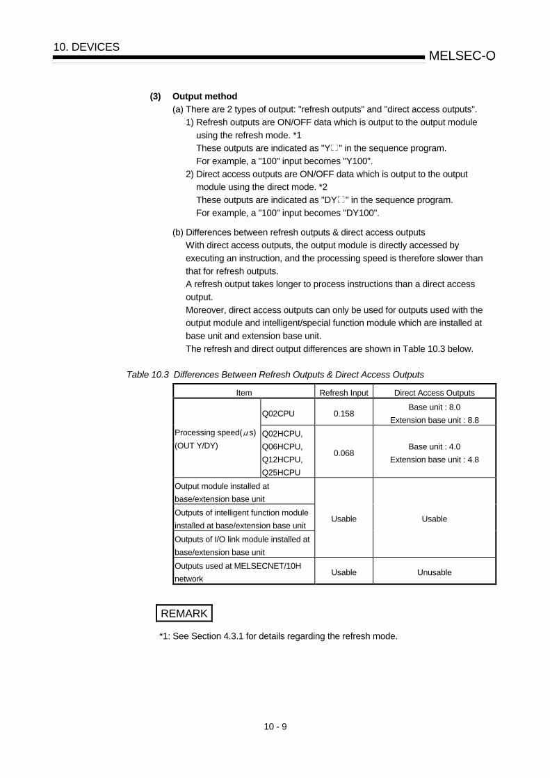
10 - 9
MELSEC-Q 10. DEVICES
(3) Output method
(a) There are 2 types of output: "refresh outputs" and "direct access outputs".
1) Refresh outputs are ON/OFF data which is output to the output module
using the refresh mode. *1
These outputs are indicated as "Y " in the sequence program.
For example, a "100" input becomes "Y100".
2) Direct access outputs are ON/OFF data which is output to the output
module using the direct mode. *2
These outputs are indicated as "DY " in the sequence program.
For example, a "100" input becomes "DY100".
(b) Differences between refresh outputs & direct access outputs
With direct access outputs, the output module is directly accessed by
executing an instruction, and the processing speed is therefore slower than
that for refresh outputs.
A refresh output takes longer to process instructions than a direct access
output.
Moreover, direct access outputs can only be used for outputs used with the
output module and intelligent/special function module which are installed at
base unit and extension base unit.
The refresh and direct output differences are shown in Table 10.3 below.
Table 10.3 Differences Between Refresh Outputs & Direct Access Outputs
Item Refresh Input Direct Access Outputs
Q02CPU 0.158 Base unit : 8.0
Extension base unit : 8.8
Processing speed( s)
(OUT Y/DY)
Q02HCPU,
Q06HCPU,
Q12HCPU,
Q25HCPU
0.068 Base unit : 4.0
Extension base unit : 4.8
Output module installed at
base/extension base unit
Outputs of intelligent function module
installed at base/extension base unit
Outputs of I/O link module installed at
base/extension base unit
Usable Usable
Outputs used at MELSECNET/10H
network Usable Unusable
REMARK
*1: See Section 4.3.1 for details regarding the refresh mode.

10 - 10
MELSEC-Q 10. DEVICES
10.2.3 Internal relays (M)
(1) Definition (a) Internal relays are auxiliary relays which cannot be latched by the
programmable controller's internal latch (memory backup).
All internal relays are switched OFF at the following times:
• When power is switched from OFF to ON.
• When a QCPU reset occurs.
• When a QCPU latch clear operation is executed.
(b) There are no restrictions regarding the number of contacts (N/O contacts, N/C
contacts) used in the program.
X0
M0
T0
Y20
X1 M0
M100
X2 M0
M2047
SET M0
K20
No restrictions regarding the quantity used.
M0 switches ON at X0 OFF to ON
The internal relay (M0) ON can only be used for internal QCPU processing, and cannot be output externally.
M0 ON/OFF information is output from the output module to an external destination.
Figure 10.5 Internal Relay
(2) Procedure for external outputs
Outputs (Y) are used to output sequence program operation results to an
external destination.
REMARK
1) Latch relays (L) should be used when a latch (memory backup) is required.
See Section 10.2.4 for details regarding latch relays.

10 - 11
MELSEC-Q 10. DEVICES
10.2.4 Latch relays (L)
(1) Definition (a) Latch relays are auxiliary relays which can be latched by the programmable
controller's internal latch (memory backup).
Latch relay operation results (ON/OFF information) are saved even in the
following cases:
• When power is switched from OFF to ON.
• When a QCPU reset occurs.
The latch is backed up by the QCPU battery.
(b) Latch relays can be switched OFF by latch clear at the QCPU. However, a
latch relay cannot be switched OFF by RESET/L.CLR key operation if latch
clear has been made ineffective for that latch relay in the device settings
parameters.
(c) There are no restrictions regarding the number of contacts (N/O contacts, N/C
contacts) used in the program.
X0
L0
T0
Y20
X1 L0
L100
X2 L0
L2047
SET L0
K20
No restrictions regarding the quantity used.
L0 switches ON at X0 OFF to ON.
The latch relay (L0) ON can only be used for internal QCPU processing, and cannot be output externally.
L0 ON/OFF information is output from the output module to an external destination.
Figure 10.6 Latch Relay
(2) Procedure for external outputs
Outputs (Y) are used to output sequence program operation results to an
external destination.
REMARK
Internal relays (M) should be used when a latch (memory backup) is not required.
See Section 10.2.3 for details regarding internal relays.

10 - 12
MELSEC-Q 10. DEVICES
10.2.5 Anunciators (F)
(1) Definition (a) Anunciators are internal relays used by the user in fault detection programs.
(b) When anunciators switch ON, a special relay (SM62) switches ON, and the
Nos. and quantity of anunciators which switched ON are stored at the special
registers (SD62 to SD79).
• Special relay :SM62.................... :Switches ON if even one anunciator
switches ON.
• Special register :SD62.................... No. of first anunciator which switched
ON is stored here.
SD63.................... The number (quantity) of anunciators
which are ON is stored here.
SD64 to SD79...... Anunciator Nos. are stored in the order
in which they switched ON.
(The same anunciator No. is stored at
SD62 and SD64.)
The anunciator No. stored at SD62 is also registered in the "fault history
area".
(c) The use of anunciators in the fault detection program permits the user to
check for the presence/absence of fault and to check the fault content
(anunciator No.), by monitoring the special registers(SD62 to SD79) when the
special relay(SM62) switches ON.
Example
The program which outputs the No. of the ON annunciator (F5) is shown below.
[Fault detection program]
SD62BCDP
SM62
SET F5
K4Y20
X0 X10
Output of annunciator No. which switched ON
Annunciator ON detection
SM62SD62SD63SD64SD65
SD79
OFF to ON0 to 50 to 10 to 5
0
0

10 - 13
MELSEC-Q 10. DEVICES
(2) Anunciator ON procedure
(a) Anunciator ON procedure
Anunciator operation can be controlled by the SET F and OUT
F instructions.
1) The SET F instruction switches the anunciator ON only at the leading
edge (OFF to ON) of the input condition, and keeps the anunciator ON
when the input condition switches OFF.
In cases where many anunciators are used, the OUT F instruction can be
used to speed up the scan time.
2) The OUT F instruction can switch the anunciator ON or OFF. It takes
longer to do so than the SET F instruction. If the anunciator is switched
OFF by using an OUT F instruction, this will require the execution of an
RST F or LEDR instruction. Use a SET F instruction to switch the
anunciator ON. POINT
(1) If switched ON by any method other than the SET F and OUT F
instructions, the anunciator functions in the same way as the internal relay.
(Does not switch ON at SM62, and anunciator Nos. are not stored at SD62,
SD64 to SD79.)
(b) Processing at anunciator ON 1) Data stored at special registers (SD62 to SD79)
a) Nos. of anunciators which switched ON are stored in order at SD64 to SD79.
b) The anunciator No. which was stored at SD64 is stored at SD62. c) "1" is added to the SD63 value.
0
0
0
0
0
0
0
SD62
SD63
SD64
SD65
SD66
SD67
SD79
50
1
50
0
0
0
0
50
2
50
25
0
0
0
50
3
50
25
2047
0
0
Up to 16 annunciator No. can be stored.
SET F50 SET F25 SET F2047
2) Processing at QCPU
"USER" LED at QCPU front is ON. (3) Anunciator OFF procedure & processing content
(a) Anunciator OFF procedure
An anunciator can be switched OFF by the RST F , LEDR, BKRST, and
OUT F instructions. 1) An anunciator No. which has been switched ON by the SET F instruction
can be switched OFF by the RST F instruction. 2) The LEDR instruction is used to switch OFF the anunciator Nos. stored at
SD62 and SD64. 3) Use the BKRST instruction if you want to switch all the anunciator Nos.
within a specified range.

10 - 14
MELSEC-Q 10. DEVICES
4) The OUT F instruction can execute ON/OFF of the anunciator No. by the
same instruction. However, if an anunciator is switched OFF by the OUT F instruction, the "processing at anunciator OFF" (item (b) below) does not occur. Execute the RST F , LEDR or BKRST instructions after the anunciator has been switched OFF by the OUT F instruction.
1) To switch OFF only the anunciators stored at SD62 and SD64:
SD62 and SD64 annuciators OFFprogram
Display reset input
LEDR
Fault detection program(Annunciator ON program)
2) To switch OFF all anunciators which are ON:
F0 K10
Display reset input
F0 to F11 OFF program
Fault detection program(Annunciator ON program)
BKRSTP
REMARK
For details regarding the LEDR and BKRST instruction, refer to the QCPU(Q
mode)/QnA Programming Manual(Common Instructions).
(b) Processing at anunciator OFF 1) Special register (SD62 to SD79) data operation at LEDR instruction
a) Anunciator No. stored at SD64 is deleted, and anunciator Nos. stored at subsequent registers (SD65 to SD79) are moved up to fill the vacant space.
b) The anunciator No. stored at SD64 is stored at SD62. c) "-1" is subtracted from the SD63 value. d) If the SD63 value is "0", SM62 is switched OFF.
0
0
0
0
0
0
0
SD62
SD63
SD64
SD65
SD66
SD67
SD79
50
1
50
0
0
0
0
50
2
50
25
0
0
0
50
3
50
25
2047
0
0
SET F50 SET F25 SET F2047
25
2
25
2047
0
0
0
LEDR

10 - 15
MELSEC-Q 10. DEVICES
2) Special register (SD62 to SD79) data operation when an anunciator is
switched OFF by the RST F instruction a) The anunciator No. which was switched OFF is deleted, and all
subsequent anunciator Nos. are moved up to fill the vacant space. b) If the anunciator No. stored at SD64 was switched OFF, the new
anunciator No. which is stored at SD64 is stored at SD62. c) "-1" is subtracted from the SD63 value. d) If the SD63 value is "0", SM62 is switched OFF.
0
0
0
0
0
0
0
SD62
SD63
SD64
SD65
SD66
SD67
SD79
50
1
50
0
0
0
0
50
2
50
25
0
0
0
50
3
50
25
2047
0
0
SET F50 SET F25 SET F2047
50
2
50
2047
0
0
0
RST F25
3) Processing at QCPU
If all SD64 to SD79 anunciator Nos. are switched OFF, the "USER" LED on the QCPU front display is switched OFF.
POINT
If an error occurs to continue operation with the higher-priority over an anunciator
when the anunciator is switched ON, eliminate the error by executing an LEDR
instruction. See Section 7.20.2 for precedence. In this case, executing an LED
instruction will not switch the anunciator OFF. To switch the anunciator OFF, you
must first eliminate the error before executing the LEDR instruction because the
error takes precedence over the anunciator.

10 - 16
MELSEC-Q 10. DEVICES
10.2.6 Edge relay (V)
(1) Definition (a) An edge relay is a device which stores the operation results (ON/OFF
information) from the beginning of the ladder block.
Edge relays can only be used at contacts, and cannot be used as coils. X0 X1 X10 V1
Edge relayStores the X0, X1 and X10 operation results
(b) The same edge relay number cannot be used twice in programs executed by
the QCPU.
(2) Edge relay applications
Edge relays are used for detecting the leading edge (OFF to ON) in programs
configured using index qualification.
SM400
[Ladder example]
X0Z1*1 V0Z1*1
SM400
Z1
M0Z1
K10
Z1
NEXT
K0
FOR
INC
MOV Index register (Z1) OFF
Repetition (10 times) designation
1 scan ON at X0 leading edge
Increment Index Register (Z1) (+1)
Return to FOR instruction
When Z1=0
X0 OFF
V0 OFF
M0 OFF
ON
ON
ON
1 Scan
[Timing chart]
When Z1=1
X1 OFF
V1 OFF
M1 OFF
ON
ON
ON
1 Scan
1 scan ON at X1 leading edge
REMARK
1) *1: The ON/OFF information for X0Z1 is stored at the V0Z1 edge relay.
For example, the X0 ON/OFF information is stored at V0, and the X1 ON/OFF
information is stored at V1.

10 - 17
MELSEC-Q 10. DEVICES
10.2.7 Link relays (B)
(1) Definition (a) A link relay is the QCPU relay used to refresh the QCPU from the
MELSECNET/10H network module's link relay (LB) and to refresh the
MELSECNET/10H network module's link relay (LB) from the QCPU data. QCPU
Link relay
B0
MELSECNET/10H network module
Link relay
LB0
Link refresh setting rangeLink refresh
Internal relays or latch relays can be used for data ranges not used by the
MELSECNET/10H network system.
• Range where no link relay latch occurs...Internal relay
• Range where link relay latch occurs........Latch relay
(b) There are no restrictions regarding the number of contacts (N/O contacts, N/C
contacts) used in the program.
X0
B0
T0
Y20
X1 B0B100
X2 B0B1FFF
SET B0
K20
No restrictions regarding the quantity used.
B0 switches ON at X0 OFF to ON.
The link relay (B0) ON can only be used for internal QCPUprocessing, and cannot be output externally.
B0 ON/OFF information is output from the output module to an external destination.
Figure 10.7 Link Relay
(2) Using link relays in the network system In order to use link relays in the network system, a network parameter setting is
required. Link relays for which no network parameter setting has been
designated can be used as internal relays or latch relays.
REMARK
1) For details regarding the network parameters, refer to the For Qs
MELSECNET/10H Network System Reference Manual.
2) The MELSECNET/10H Network Module has 16384 link relay points assigned.
QCPU has 8192 link relay points assigned. When using subsequent points after
Point 8192, change the number of link relay points by using the GPPW (the
Device Setting sheet of the PLC Parameter dialog box).
10 - 18
MELSEC-Q 10. DEVICES
10.2.8 Special link relays (SB)
(1) Definition (a) A special link relay indicates the communication status and error detection of
an intelligent function module, such as the MELSECNET/10H Network
Module.
(b) Because special link relays are switched ON and OFF in accordance with
various problems which may occur during a data link, they serve as a tool for
identifying data link problems.
(2) Number of special link relay points
There are a total of 2048 special link relay points between SB0 and SB7FF.
Special link relays are assigned at a rate of 512 points per each intelligent
function module, such as the MELSECNET/10H Network Module. Special link
relays are assigned as shown below.
For 1st network module
For 2nd network module
For 3rd network module
For 4th network module
SB200
SB3FFSB400
SB5FFSB600
SB7FF
SB0
SB1FF
512 points
512 points
512 points
512 points
2048 points
REMARK
1) For details regarding special link relays used at the QCPU, refer to the QCPU (Q
mode)/QnACPU Programming Manual (Common Instructions).
10.2.9 Step relays (S)
A step relay is an SFC program device.
For details regarding procedures for using step relays, refer to the QCPU (Q
mode)/QnACPU Programming Manual (SFC).
POINT
Because the step relay is a device exclusively for the SFC program, it cannot be
used as an internal relay in the sequence program.
If used in this manner a SFC error will occur, and system operation will be stopped
(system down).

10 - 19
MELSEC-Q 10. DEVICES
10.2.10 Timers (T)
Timers are of a forward timer type, with the time measurement beginning when the coil
switches ON, and ending (time out) when the present value exceeds the setting value.
The present value matches the setting value when a "time-out" occurs.
There are two types of timers: a low/high-speed that allows the current value to return
to "0" when a timer coil switches OFF, and a retentive timer that retains the current
value even when a timer coil switches OFF. Timers Timers Low-speed timers
High-speed timers
Retentive timers Low-speed retentive timers
High-speed retentive timers With a timer setting (instruction format), a device is assigned for a low-speed timer or
high-speed timer. The OUT T0 instruction is used to assign a device for a low -speed
timer. The OUTH T0 instruction is used to assign a device for a high-speed timer.
With a timer setting (instruction format), a device is assigned for a low-speed retentive
timer or high-speed retentive timer. The OUT T0 instruction is used to assign a device
for a low-speed retentive timer. The OUTH T0 instruction is used to assign a device for
a high-speed retentive timer.
Low-speed timers
(1) Definition (a) Low-speed timers are those that are only operative while the coil is ON.
(b) The time measurement begins when the timer's coil switches ON, and the
contact switches ON when a "time-out" occurs. When the timer's coil
switches OFF, the present value becomes "0", and the contact switches OFF.
X0
T0
K10[Ladder example]
When X0 switches ON, the T0 coil switches ON, and the contact switches ON 1 second later. (The low-speed timer measures time in 100 ms units.)
T0 coil
OFF
OFF
OFF
ON
ON
ON1 Sec.
[Time chart]
X0
T0 contact
(2) Measurement units (a) The default time measurement units setting for low-speed timers is 100 ms.
(b)The time measurement units setting can be designated in 1 ms units within a 1
ms to 1000 ms range.
This setting is designated in the "PLC system settings" in the PLC parameter
setting.

10 - 20
MELSEC-Q 10. DEVICES
High-speed timers
(1) Definition (a) High-speed timers are timers which are only operative while the coil is ON. A
high-speed timer is marked with a symbol "H".
(b) The time measurement begins when the timer's coil switches ON, and the
contact switches ON when the time elapses. When the timer's coil switches
OFF, the present value becomes "0", and the contact switches OFF.
X0 H
[Ladder example]
When X0 switches ON, the T200 coil switches ON, andthe contact switches ON 2 second later. (The high-speedtimer measures time in 10 ms units.)
K200
T200
High-speed timer display
T200 coil
OFF
OFF
OFF
ON
ON
ON2 Sec.
[Time chart]
X0
T200 contact
(2) Measurement units (a) The default time measurement units setting for high-speed timers is 10 ms.
(b) The time measurement units setting can be designated in 0.1ms units within a
0.1 ms to 100 ms range.
This setting is designated in the PLC system settings in the PLC parameter
setting.

10 - 21
MELSEC-Q 10. DEVICES
Retentive timers *
(1) Definition (a) Retentive timers measure the "coil ON" time.
(b) The measurement begins when the timer coil switches ON, and the contact
switches ON when a time-out (coil OFF) occurs.
Even when the timer coil is OFF, the present value and the contact ON/OFF
status are saved. When the coil is switched ON again, the time measurement
resumes from the present value which was saved.
(c) There are 2 retentive timer types: low-speed retentive timer, and high-speed
retentive timer.
(d) The RST T instruction is used to clear (reset) the present value and switch
the contact OFF.
X1RST ST0
X0
ST0
K200[Ladder example]
When X1 switches ON, the ST0 contact is reset, and the present value is cleared.
X0 ON time is measured as 20 seconds when the timer measures time in 100 ms units.
Retentive timer display
T0 coil
OFF
OFF
ON
ON
ON
15 Sec.
[Time chart]
X0
T0 present value
OFF
OFF
0 to1 151 200to
5 Sec.
0
Contact remains ON when coil switches.
Present value is saved when coil switches.
X1
T0 contact
RST ST0 instruction
150
Instruction execution
ON
(2) Measurement units (a) The measurement units settings for retentive timers are the same as those for
low-speed timers and high-speed timers.
• Low-speed retentive timer: Same as low-speed timer
• High-speed retentive timer: Same as high-speed timer
REMARK
1) *: In order to use retentive timers, a retentive timer "number of points used" setting
must be designated in the PLC parameters device settings.

10 - 22
MELSEC-Q 10. DEVICES
Timer Processing & accuracy
(a) When an OUT T instruction is executed, the following processing occurs:
timer coil ON/OFF, present value update & contact ON/OFF processing.
Timer present value update and contact ON/OFF processing do not occur at
END processing.
Processing content Coil ON/OFF Present value update Contact ON/OFF
X0
T0
K10[Ladder example]
Sequence
program
END OUT T0 END
[Processing at OUT T0 instruction]
(b) When the OUT T instruction is executed, the present value is added to the
scan time measured at the END instruction.
If the timer coil is OFF when the OUT T instruction is executed, the present
value is not updated.
X0
T0
H[Ladder example]
K8
QCPU's X0
21 1 1 2 1 1 2 1
2 3 2 3 2 3
2+3=50+2=2 5+2=7 7+3=10
OUT T0END processing
OUT T0 OUT T0 OUT T0 OUT T0 OUT T0
Input reading timing (+1 scan)
Timer accuracy (+1 scan)
Program
X0 external input
T0 coil
210 ms measurement
T0 contact
Measured value at END instruction
T0 present value
[Present value update timing]
ON
OFF
OFF
OFF
ON
ON
OFFON
3 2 3 2 3
END processing
END processing
END processing
END processing
END processing
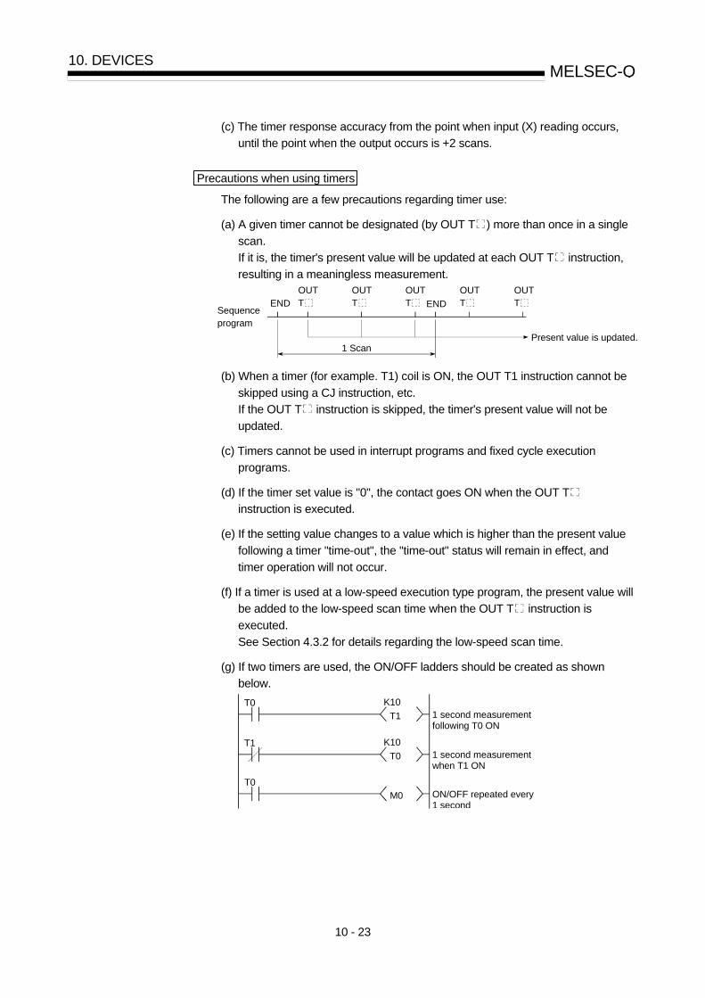
10 - 23
MELSEC-Q 10. DEVICES
(c) The timer response accuracy from the point when input (X) reading occurs,
until the point when the output occurs is +2 scans.
Precautions when using timers
The following are a few precautions regarding timer use:
(a) A given timer cannot be designated (by OUT T ) more than once in a single
scan.
If it is, the timer's present value will be updated at each OUT T instruction,
resulting in a meaningless measurement.
Sequence program
END END
OUTT
OUTT
OUTT
OUTT
Present value is updated.1 Scan
OUTT
(b) When a timer (for example. T1) coil is ON, the OUT T1 instruction cannot be
skipped using a CJ instruction, etc.
If the OUT T instruction is skipped, the timer's present value will not be
updated.
(c) Timers cannot be used in interrupt programs and fixed cycle execution
programs.
(d) If the timer set value is "0", the contact goes ON when the OUT T
instruction is executed.
(e) If the setting value changes to a value which is higher than the present value
following a timer "time-out", the "time-out" status will remain in effect, and
timer operation will not occur.
(f) If a timer is used at a low-speed execution type program, the present value will
be added to the low-speed scan time when the OUT T instruction is
executed.
See Section 4.3.2 for details regarding the low-speed scan time.
(g) If two timers are used, the ON/OFF ladders should be created as shown
below.
T0
M0
T1T0
K10
T0
T1
K101 second measurement following T0 ON
1 second measurement when T1 ON
ON/OFF repeated every 1 second

10 - 24
MELSEC-Q 10. DEVICES
10.2.11 Counters (C)
Counters are "up counter" types, with the contact being switched ON when the count
value equals the setting value (count-out condition).
There are two counter types: counters which count the number of input condition start-
ups (leading edges) in sequence programs, and counters which count the number of
interrupt factor occurrences.
Counters
(1) Definition A counter is a device which counts the number of input condition leading edges
in sequence programs.
(2) Count processing
A counter is a device which counts the number of input condition leading edges
in sequence programs.
(a) When and OUT C instruction is executed, the following counter processing
occurs: coil ON/OFF, present value update (count value + 1), and contact
ON/OFF.
Counter present value update and contact ON/OFF processing do not occur
at END processing.
Processing content
Coil ON/OFF
Present value update
Contact ON/OFF
X0C0
K10[Ladder example]
Sequence
program
END OUT C0 END
[Processing at OUT C0 Instruction (X0: OFF to ON)]
(b) The present value update (count value + 1) occurs at the leading edge (OFF
to ON) of the OUT C instruction.
The present value is not updated in the following OUT C instruction
statuses: OFF, ON to ON, ON to OFF
X0
C0
K10[Ladder example]
X0 OFF
OFF
ON
ON
[Present value update timing]
END END ENDOUT C0 OUT C0 OUT C0
Present value update Present value update
Sequence program
C0 coil

10 - 25
MELSEC-Q 10. DEVICES
(c) Multiple counters can be used within a single scan to achieve the maximum
counting speed.
In such cases, the direct access input (DX ) method should be used for the
counter input signals.*1 OUTC
Sequence program
END END
OUT C execution intervals
OUTC
OUTC
OUTC
OUTC
(3) Resetting the counter (a) Counter present values are not cleared even if the OUT C instruction
switches OFF. Use the RST C instruction to clear the counter's present
value and switch the contact OFF. (b) The count value is cleared and the contact is switched OFF at the point when
the RST C instruction is executed.
X0
[Ladder example]
RST C0
X0 OFF
OFF
ON
Execution
[Counter reset timing]
END END ENDRST C0 RST C0 RST C0
Count value cleared & contact OFF Count value cleared & contact OFF
Sequence program
RST C0 instruction
(4) Maximum counting speed The counter can count only when the input condition ON/OFF time is longer than
the execution interval of the corresponding OUT C instruction.
The maximum counting speed is calculated by the following formula:
= n
1001T
[times/sec]Maximum counting speed (Cmax)
n: Duty(%) *2
T: Execution interval of the OUT C instruction
REMARK
1) *1: See Section 10.2.1 for details regarding direct access inputs.
2) *2: The "duty" is the count input signal's ON-OFF time ratio expressed as a
percentage value.
Count input signal OFF
ON
T1 T2
When T1 T2 n = 100T1+T2
T1
T1+T2T2When T1 < T2 n = 100

10 - 26
MELSEC-Q 10. DEVICES
Interrupt counters
(1) Definition Interrupt counters are devices which count the number of interrupt factor
occurrences.
(2) Count processing
(a) The interrupt counter's present value is updated when an interruption occurs.
It is not necessary to create a program which includes an interrupt counter
function. (b) Interrupt counter operation requires more than the simple designation of a
setting value.
To use the interrupt counter for control purposes, comparison instructions (=,
<=, etc.) must also be used to enable comparisons with the setting value, with
an internal relay (M), etc., being switched ON or OFF according to the
comparison result.
The figure below shows a sample program in which M0 is switched ON after
10 interrupt inputs occur. (In this example, "C300" is the interrupt counter No.
corresponding to I0.) = K10 C300 M0
(3) Setting the interrupt counter (a) In order to use interrupt counters, at first interrupt counter No. setting must be
designated in the PLC system settings in the PLC parameter setting.
256 points are then allocated for interrupt counters, beginning from the "first
counter No." which is designated.
If C300 is designated as the first interrupt counter No., numbers C300 to
C555 will be allocated for interrupt counters. I0
I1
I2
I255
C300
C301
C302
C555
Interrupt counter (256 points)
Values corresponding to the interrupt counter No. (b) In order to use an interrupt counter, an "interruption permitted" status must be
established by E1 instruction at the main routine program.

10 - 27
MELSEC-Q 10. DEVICES
(4) Precautions
(a) One interrupt pointer is insufficient to execute interrupt counter and interrupt
program operation.
Moreover, an interrupt program cannot be executed by an interrupt counter
setting designated in the PLC system settings in the PLC parameter setting.
(b) If the processing items shown below are in progress when an interruption
occurs, the counting operation will be delayed until processing of these items
is completed.
The count processing starts after the execution of programs is completed.
Even if the same interruption occurs again while processing of these items is
in process, only one interruption will be counted.
• During execution of sequence program instructions
• During interrupt program execution
• During execution of a fixed scan execution type program
(c) The maximum counting speed of the interrupt timer is determined by the
longest processing time of the items shown below.
• Instruction with the longest processing time among the instructions used in
the program
• Interrupt program processing time
• The processing time of a fixed scan execution type program
(d) The use of too many interrupt counters will increase the sequence program
processing time, and may cause a "WDT ERROR".
If this occurs, either reduce the number of interrupt counters, or reduce the
counting speed for the input pulse signal.
(e) The interrupt counter's count value can be reset by using the RST C
instruction in the sequence program prior to the FEND instruction.
(f) The interrupt counter's count value can be read out by using the sequence
program MOV instruction.
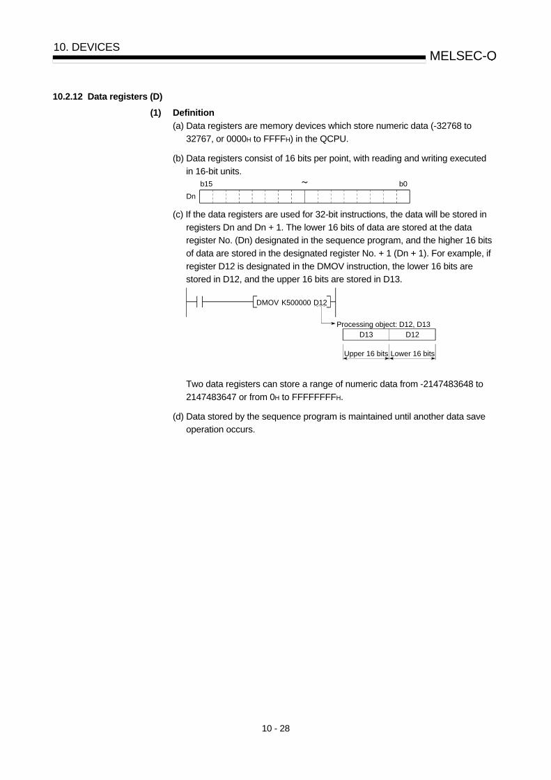
10 - 28
MELSEC-Q 10. DEVICES
10.2.12 Data registers (D)
(1) Definition (a) Data registers are memory devices which store numeric data (-32768 to
32767, or 0000H to FFFFH) in the QCPU.
(b) Data registers consist of 16 bits per point, with reading and writing executed
in 16-bit units.
Dn
b15 b0
(c) If the data registers are used for 32-bit instructions, the data will be stored in
registers Dn and Dn + 1. The lower 16 bits of data are stored at the data
register No. (Dn) designated in the sequence program, and the higher 16 bits
of data are stored in the designated register No. + 1 (Dn + 1). For example, if
register D12 is designated in the DMOV instruction, the lower 16 bits are
stored in D12, and the upper 16 bits are stored in D13.
K500000 D12DMOV
D13
Upper 16 bits Lower 16 bits
D12Processing object: D12, D13
Two data registers can store a range of numeric data from -2147483648 to
2147483647 or from 0H to FFFFFFFFH.
(d) Data stored by the sequence program is maintained until another data save
operation occurs.

10 - 29
MELSEC-Q 10. DEVICES
10.2.13 Link registers (W)
(1) Definition (a) A link register is the QCPU memory used to refresh the QCPU with data from
the link registers (LW) of intelligent function modules including
MELSECNET/10H network module.
Link registers are used to store numeric data (-32768 to 32767, or 0000H to
FFFFH) at the QCPU. QCPU
Link register
W0
MELSECNET/10H network module
Link register
LW0Link refresh setting rangeLink refresh
When used outside the MELSECNET/10H network system's range, link
registers can serve as data registers.
(b) Link registers consist of 16 bits per point, with reading and writing executed in
16-bit units.
Wn
b15 b0
(c) If the link registers are used for 32-bit instructions, the data is stored in
registers Wn and Wn + 1. The lower 16 bits of data are stored in the link
register No. (Wn) designated in the sequence program, and the higher 16 bits
of data are stored in the designated register No. + 1 (Wn + 1).
For example, if link register W12 is designated at the DMOV instruction, the
lower 16 bits are stored in W12, and the upper 16 bits are stored in W13.
K500000 W12DMOV
W13
Upper 16 bits Lower 16 bits
W12Processing object: W12, W13
In two link register points, -2147483648 to 2147483647 or OH to FFFFFFFFH
data can be stored. (d) Data stored by the sequence program is maintained until another data save
operation occurs.
REMARK
The MELSECNET/10H network module has 16384 link register points. The QCPU
has 8192 link register points. When subsequent points after Point 8192 are used for
link registers, change a "number of points" setting of link registers on the GPPW side
(in the Device sheet of the PLC Parameter dialog box).

10 - 30
MELSEC-Q 10. DEVICES
(2) Using link registers in a network system
In order to use link registers in the network system, network parameter settings
must be made.
Link registers not set in the network parameter settings can be used as data
registers.
REMARK
1) For details regarding network parameters, refer to the For Qs MELSECNET/10H
Network System Reference Manual.
10.2.14 Special link registers (SW)
(1) Definition (a) Special link registers are used to store data on the communication status and
errors of an intelligent function
(b) Because the data link information is stored as numeric data, the special link
registers serve as a tool for identifying the locations and causes of faults.
(2) Number of special link register points
There are 2048 special link register points from SW0 to SW7FF. The special link
register points are assigned at the rate of 512 points per intelligent function
module, such as a MELSECNET/10H network module.
By default, the following points are assigned for link registers as shown below.
For the 1st network module
For the 2nd network module
For the 3rd network module
For the 4th network module
SW200
SW3FFSW400
SW5FFSW600
SW7FF
SW0
SW1FF
Special register for the link
512 points
512 points
512 points
512 points
2048 points
REMARK
For details regarding special link registers used in the QCPU, refer to the QCPU(Q
mode)/QnACPU Programming Manual (Common Instructions).

10 - 31
MELSEC-Q 10. DEVICES
10.3 Internal System Devices
Internal system devices are devices used for system operations.
The allocations and sizes of internal system devices are fixed, and cannot be changed
by the user.
10.3.1 Function devices (FX, FY, FD)
(1) Definition (a) Function devices are devices used in sub-routine programs with arguments to
permit data transfers between the sub-routine program with argument, and
the CALL source for that sub-routine. Example
If FX0 and FD1 are used at the sub-routine program, and if M0 and D0 are designated by the sub-routine CALL instruction, the M0 ON/OFF data is transferred to FX0, and the D0 data is transferred to FD1.
[Sub-routine program CALL source]
M0 D0P0CALL FD1 R0MOV
RET
X0 FX0P0
[Sub-routine program]
(b) Because the function devices used for each sub-routine program CALL
source can be set, the same sub-routine program can be used without regard
to other sub-routine CALL sources.
(2) Types of function devices
There are 3 function device types: function input devices (FX), function output
devices (FY), and function register devices (FD).
(a) Function input devices (FX)
• These devices are used to designate inputs of ON/OFF data to a sub-
routine program.
• In the sub-routine program, these devices are used for reading and
processing bit data designated by sub-routine with argument CALL
instruction.
• All the QCPU bit data designation devices can be used.
(b) Function output devices (FY)
• These devices are used to designate outputs of sub-routine program
operation results (ON/OFF data) to the sub-routine program CALL source.
• At sub-routine programs with arguments, the operation results are stored at
the designated device.
• All bit data designation devices except QCPU inputs (X, DX) can be used.

10 - 32
MELSEC-Q 10. DEVICES
(c) Function registers
• Function registers are used to designate data transfers between the sub-
routine CALL source and the sub-routine program.
• The function register input/output condition is automatically determined by
the QCPU. If the sub-routine program data is the source data, the data is
designated as sub-routine input data.
If the sub-routine program data is the destination data, the data is
designated as sub-routine output data.
• 1 point occupies 4 words.
The number of words used depends on an instruction in a sub-routine
program. A one-word instruction requires 1 word.
CALLP P0 D0 MOV R0 PD0P0
The data is stored in one point (D0). A two-work instruction requires 2 words.
DMOV R0 PD0CALLP P0 D0 P0
The data is stored in two points (D0 and D1). The destination of 32-bit multiplication/division operation requires 4 words.
CALLP P0 D0 D* R0 R10 PD0P0
The data is stored in four points (D0 to D3).
• Active devices cannot be used in a sub-routine program that contains
arguments. If devices assigned for function registers are used, values of the
function registers will not properly be returned to a calling program.
CALLP P0 D0 D* R0 R10 PD0P0
MOV K0 D3
Since the points (D0 to D3) are used for FD0, D3 can not be used for the sub-routine program.
• QCPU's word data devices can be used.
REMARK
1) For a procedure for using function devices, see the QCPU (Q Mode)/QnACPU
Programming Manual (Common Instructions).

10 - 33
MELSEC-Q 10. DEVICES
10.3.2 Special relays (SM)
(1) Definition (a) A special relay is used to store QCPU status data.
(2) Special relay classifications
Special relays are classified according to their applications, as shown below.
(a) For fault diagnosis : SM0 to SM199
(b) System information : SM200 to SM399
(c) System clock/system counter : SM400 to SM499
(d) Scan information : SM500 to SM599
(e) Memory card information : SM600 to SM699
(f) Instruction related : SM700 to SM799
(g) For debugging : SM800 to SM899
(h) Latch area : SM900 to SM999
(i) For ACPU : SM1000 to SM1299*
REMARK
1) For details regarding special relays which can be used by the QCPU, refer to
Appendix 1.
2) *: This takes effect only after you have turned on the "Use special relay/special
register form SM1000/SD1000" check box in the "Compatibility with A-PLC"
section in the PLC System sheet of the PLC Parameter dialog box.

10 - 34
MELSEC-Q 10. DEVICES
10.3.3 Special registers (SD)
(1) Definition (a) A special register is used to store QCPU status data (diagnosis and system
information).
(2) Special register classifications
Special registers are classified according to their applications, as shown below.
(a) For fault diagnosis : SD0 to SD199
(b)System information : SD200 to SD399
(c) System clock/system counter : SD400 to SD499
(d) Scan information : SD500 to SD599
(e) Memory card information : SD600 to SD699
(f) Instruction related : SD700 to SD799
(g)For debugging : SD800 to SD899
(h) Latch area : SD900 to SD999
(i) For ACPU : SD1000 to SD1299*
(j) Fuse-blown module : SD1300 to SD1399
(k) Check of input/output modules : SD1400 to SD1499
REMARK
1) For details regarding special relays which can be used by the QCPU, refer to
Appendix 2.
2) *: This takes effect only after you have turned on the "Use special relay/special
register form SM1000/SD1000" check box in the "Compatibility with A-PLC"
section in the PLC System sheet of the PLC Parameter dialog box.

10 - 35
MELSEC-Q 10. DEVICES
10.4 Link Direct Devices (J \ )
(1) Definition (a) At END processing, a data refresh (data transfer) operation occurs between
the QCPU and the MELSECNET/10H network system modules. Link direct devices are used at that time to directly access the link devices in the MELSECNET/10H network modules.
(b) Designation method
• Link direct devices are designated by network No. and device No. Designation method: J \
Device No.
Input...........................X0
Output........................Y0
Link relay.................. B0
Link register...............W0
Link special relay.......SB0
Link special register ..SW0Network No.(1 to 255)
• For link register 10 (W10) of network No.2, the designation would be "J2\W10"
K100 J2W10MOVPNetwork modules at network No.2
W 0
W10
• For a bit device (X, Y, B, SB), digit designation is necessary.
Designation example : J1\K1X0, J10\K4B0 (2) Designation range
Link direct device designations are possible for all the link devices in network modules.
Device outside the range specified by the network refresh parameters can also be designated.
(a) Writing 1) Writing is executed within that part of the link device range set as the send
range in the common parameters of the network parameters that is outside the range specified as the "refresh range" in the network refresh parameters.
Refresh range
QCPU Network module
LB 0B 0
send range
Link range
Writing range

10 - 36
MELSEC-Q 10. DEVICES
2) Although writing is also possible in the "refresh range" portion of the link
device range (specified by the refresh parameters), the link module's link device data will be rewritten when a refresh operation occurs. Therefore, when writing by link direct device, the same data should also be written to the QCPU related devices designated by the refresh parameters.
[Sequence program]
"100" is written to link module LW1 when the MOV instruction is executed.
MOV K100 W1
MOV W1 J1\W1
"100" is written to link module LW1 when a refresh occurs.
[Writing timing]
MOV K100
MOV
Writing at instruction execution
W0W1 LW1
Writing at instruction execution
QCPU Network module
Writing at refresh operation
W1
W1 J1\W1
[Refresh parameter settings] Network No. : 1 QCPU(W0 to W3F) Network module (LW0 to LW3F)
3) When data is written to another station's writing range using a link direct
device, the data which is received from that station will replace the written data.
(b) Reading
Reading by link direct device is possible in the entire link device range of network modules.
POINT
(1) Only one network module capable of writing/reading link direct devices can be
used per network number.
If two or more network modules are installed at the same network number, the
network module with the lowest first I/O number will be the one that handles
writing/reading using link direct devices.
For example, if station No.1 and station No.2 network modules are installed in
network No.1 as shown in the figure below, the station No.2 network module will
handle link direct device operations.
Pow
er s
uppl
y m
odul
e
Station No.2
Network No.1
Writing/reading using link direct devices not possible
Writing/reading using link direct devices possible
Net
wor
k m
odul
e
Station No.1
QC
PU
Net
wor
k m
odul
e
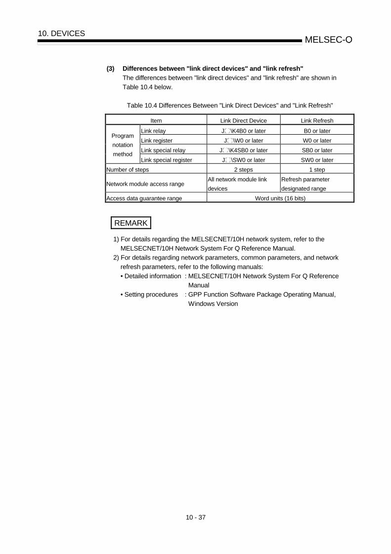
10 - 37
MELSEC-Q 10. DEVICES
(3) Differences between "link direct devices" and "link refresh"
The differences between "link direct devices" and "link refresh" are shown in
Table 10.4 below.
Table 10.4 Differences Between "Link Direct Devices" and "Link Refresh"
Item Link Direct Device Link Refresh
Link relay J \K4B0 or later B0 or later
Link register J \W0 or later W0 or later
Link special relay J \K4SB0 or later SB0 or later
Program
notation
method Link special register J \SW0 or later SW0 or later
Number of steps 2 steps 1 step
Network module access range All network module link
devices
Refresh parameter
designated range
Access data guarantee range Word units (16 bits)
REMARK
1) For details regarding the MELSECNET/10H network system, refer to the
MELSECNET/10H Network System For Q Reference Manual.
2) For details regarding network parameters, common parameters, and network
refresh parameters, refer to the following manuals:
• Detailed information : MELSECNET/10H Network System For Q Reference
Manual
• Setting procedures : GPP Function Software Package Operating Manual,
Windows Version

10 - 38
MELSEC-Q 10. DEVICES
10.5 Intelligent Function Module Devices (U \G )
(1) Definition (a) The intelligent function module devices allow the QCPU to directly access the
buffer memories of intelligent function modules/special function modules which are installed at the main base unit and extension base unit.
(b) Intelligent function module devices are designated by the intelligent/special
function module input/output No., and the buffer memory address. Designation method: U \G
Buffer memory address (setting range: 0 to16383 (decimal)) 1
Intelligent function module/special function module I/O No.
Setting: If the input/output No. is a 3-digit value, designate the first 2 digits.
For X/YF0.....X/Y1F0
Designate "1F"
Setting range: 00H to FEH When digital output values of channels (CH.1 to CH.4) of the Q64AD Type Analog-Digital Conversion Module (X/Y0 to X/YF) installed in Slot 0 of the main base unit are stored in D0 to D3, the output/input number and the buffer memory address are specified as shown below.
U0\G11 D0BMOVQ64AD
12
13
CH.1 Digital output value11
14
CH.2 Digital output value
CH.3 Digital output value
CH.4 Digital output value
K4
(2) Processing speed
The processing speed for intelligent function module devices is; (a) The processing speed of reading data from and to the buffer memory of an
intelligent-function module/special-function module is the same as that of executing the FROM/TO instruction as is the case with "M0V U0\G11 D0".
(b) The processing speed of reading data from the buffer memory of an
intelligent- function module/special-function module and performing other process is a sum of the "FROM/TO instruction processing speed" and the "instruction processing speed" as is the case with "+ U0\G11 D0 D10".
If the same buffer memory of the same intelligent function module/special function module is used two or more times in a sequence program, the processing speed can be increased by using the FROM instruction to read that buffer memory data to a QCPU device.
REMARK
1) *1: For details regarding buffer memory addresses and applications, refer to the manual for the intelligent function module/special function module in question.

10 - 39
MELSEC-Q 10. DEVICES
10.6 Index Registers (Z)
(1) Definition (a) Index registers are used in the sequence program for indirect setting (index
qualification) designations.
An index register point is used for index modification.
Index registers consist of 16 bits per point.
X0K5 Z0MOVP
SM400D0Z0 K4Y30BCD
(b) There are 16 index registers (Z0-Z15).
(c) Index registers consist of 16 bits per point, with reading and writing occurring
in 16-bit units.
Zn
b15 b0
(d) If the index registers are used for 32-bit instructions, the data is stored in
registers Zn and Zn +1.
The lower 16 bits of data are stored in the index register No. (Zn) designated
in the sequence program, and the upper 16 bits of data are stored in the
designated index register No. + 1.
For example, if register Z2 is designated in the DMOV instruction, the lower
16 bits are stored in Z2, and the upper 16 bits are stored at Z3.
D0 Z2DMOV
Z3
Upper 16 bits Lower 16 bits
Z2
Processing object: Z2, Z3

10 - 40
MELSEC-Q 10. DEVICES
10.6.1 Switching between scan execution type programs and low-speed execution type programs
When switching from a scan execution type programs or low-speed execution type
program to another program type, the index register (Z0 to Z15) data is saved
(protected) and reset.
(1) Index register processing at switching between scan execution type
programs and low-speed execution type programs
(a) When switching from a scan execution type program to a low-speed
execution type program occurs, the scan execution type program's index
register data is saved, and the low-speed execution type program's index
register data is reset.
(b) When switching from a low-speed execution program to a scan execution
type program occurs, the low-speed execution type program's index register
data is saved, and the scan execution type program's index register data is
reset.
Executed program
Index register value
Index register
storage area
Scan execution type program
Switch-ing
Z0=1
Low-speed execution type program
Z0=3
Z0=0
Z0=0
Z0=1
Z0=0
Z0=1
Z0=0
Z0=1
Z0=3
Z0=1
Z0=3
Z0=6
Z0=3
Z0=6
Z0=3
Saved Reset Saved Reset Saved Reset
Z0=0 to Z0=3*1
*1: For low-speed execution type program, Z0 is changed to 3.
*2: For scan execution type program, Z0 is changed to 6.
Z0=1 to Z0=6*2
For low-speed execution type program
For scan execution type programs
Scan execution type program
Low-speed execution type program
Switch-ing
Switch-ing
(2) Exchanges of index register data Word devices should be used for exchanges of index register data between scan execution type programs and low-speed execution type programs.
REMARK
1) For details regarding index qualifications using the index registers, refer to the
QCPU(Q mode)/QnACPU Programming Manual (Common Instructions).

10 - 41
MELSEC-Q 10. DEVICES
10.6.2 Switching between scan/low-speed execution type programs and interrupt/fixed scan execution
type programs
The PLC System sheet of the PLC Parameter dialog box provides the option to save
(protect) or restore index register data (Z0 to Z15) when switching between a scan
execution type program and a low-speed execution type program or between an
interrupt program and a fixed scan execution type program.
If you do not want to write date onto index registers when using an interrupt
program/fixed scan execution type program, turn on the "High speed execution" check
box in the "Interrupt program/Fixed scan program setting" section of the PLC System
sheet in the PLC Parameter dialog box. This will enable you to switch between
programs quickly.
(1) When the "High-speed execution" check box is OFF:
(a) When the scan/low-speed execution type program is switched to the
interrupt/fixed cycle execution type program, the scan/low-speed execution
type program's index register value is first saved, and is then transferred to
the interrupt/fixed scan execution type program.
(b) When the interrupt/fixed scan execution type program is switched to the
scan/low-speed execution type program, the saved index register value is
reset.
Executed program
Index register value
Scan/low-speed execution type program
Switch-ing
Z0=1
Z0=0 Z0=1
Index register storage area
For scan/low-speed execution type program
Interrupt program/Fixed scan executiontype program
Z0=1 to Z0=3
Z0=1
Reset
Z0=1
Z0=1
Z0=1
Scan/low-speed execution type program
*
Saved Reset
Transf-erred
*: For interrupt program, Z0 is changed to 3.
Word devices should be used to transfer index register data from an
interrupt or fixed scan execution type program to a scan or low-speed
execution type program.

10 - 42
MELSEC-Q 10. DEVICES
(2) When the "High-speed execution" check box is ON:
(a) If a scan execution type program/low-speed execution type program is
switched to an interrupt program/fixed scan execution type program, index
register data will not be saved/restored.
(b) If data is written onto index registers by using an interrupt program/fixed scan
execution type program, the values of index registers used for an scan/low-
speed execution type program will be corrupted.
Executed program
Index register value
Scan/low-speed execution type program
Z0=1
Z0=0 Z0=0
Index register storage area
For scan/low-speed execution type program
Interrupt program/Fixed scan execution type program
Z0=1 to Z0=3
Z0=0
Reset
Z0=0
Z0=3
Z0=0
Scan/low-speed execution type program
*
*: For interrupt program, Z0 is changed to 3.
Switch-ing
Transf-erred
Transf-erred
(c) Before writing data onto index registers by using an interrupt program/fixed
scan execution type program, use the ZPUSH/SPOP instruction to
save/restore the data.
ZPUSH D0SM400
ZPOP D0SM400
IRET
The points after D0 store the data (Z0 to Z15).
The data after D0 is stored in points (Z0 to Z15).
I0

10 - 43
MELSEC-Q 10. DEVICES
10.7 File Registers (R)
(1) Definition (a) File registers are expansion devices for data registers.
(b) File register data is stored in files in the QCPU standard RAM, the QCPU
memory card.
1) The standard RAM has 32k points assigned for file registers. File
registers can be used at the same processing speed as data registers.
2) Use a memory card if 32k or more points are assigned for file registers.
K100 R2MOV
"100" is written to R2.
Standard RAM/Memory card
File register
R0
R1
R2
(c) File registers consist of 16 bits per point, with reading and writing occurring in
16-bit units.
Rn
b15 b0
(d) If the file registers are used for 32-bit instructions, the data will be stored in
registers Rn and Rn + 1.
The lower 16 bits of data are stored in the file register No. (Rn) designated in
the sequence program, and the upper 16 bits of data are stored in the
designated file register No.+ 1.
For example, if file register R2 is designated in the DMOV instruction, the
lower 16 bits are stored in R2, and the upper 16 bits are stored in R3.
D0 R2DMOV
R3
Upper 16 bits Lower 16 bits
R2
Processing object: R2, R3
Two file registers can be used to store numeric data from -2147483648 to
2147483647 or from 0H to FFFFFFFFH.
(e) Data stored in a file register is retained even after power is turned on or reset.
A file register cannot be initialized with a latch clear. Use a sequence program
if you want to initialize file registers when power is turned off or reset.
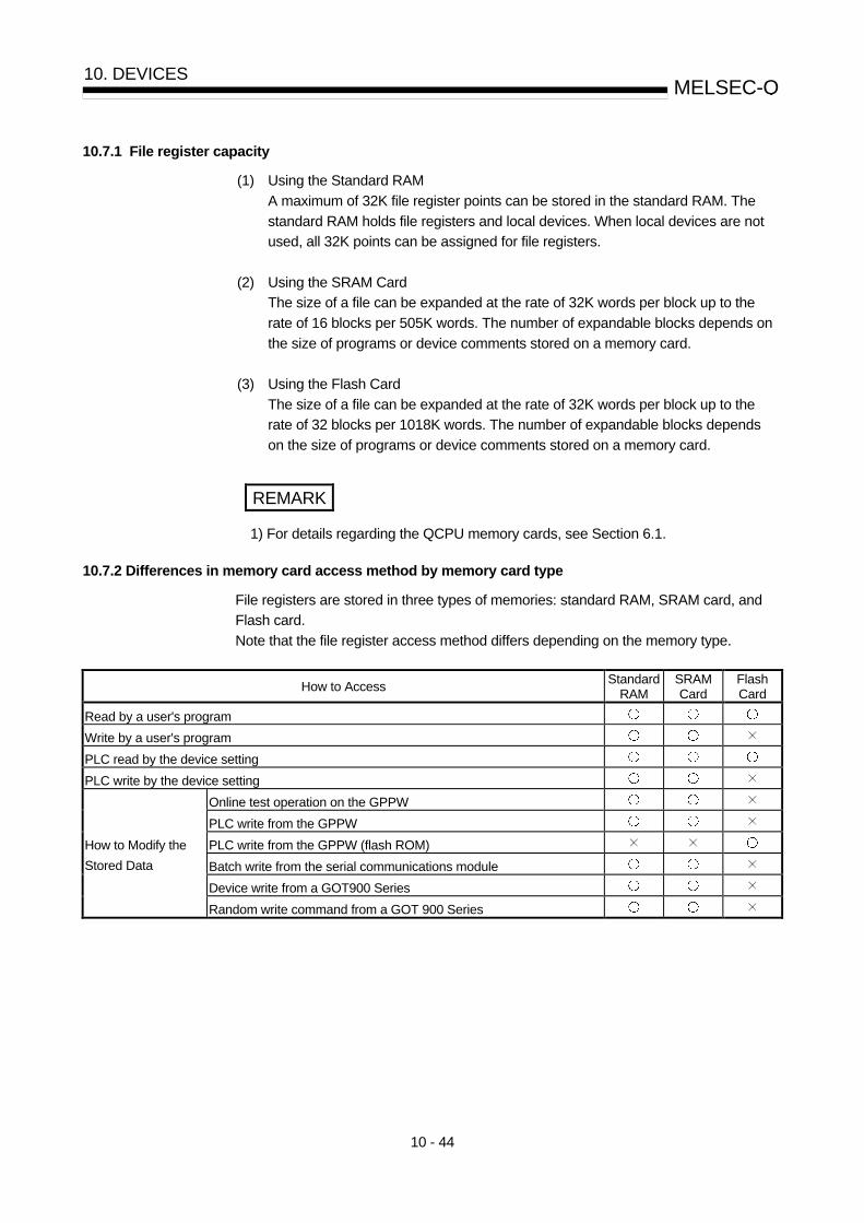
10 - 44
MELSEC-Q 10. DEVICES
10.7.1 File register capacity
(1) Using the Standard RAM
A maximum of 32K file register points can be stored in the standard RAM. The
standard RAM holds file registers and local devices. When local devices are not
used, all 32K points can be assigned for file registers.
(2) Using the SRAM Card
The size of a file can be expanded at the rate of 32K words per block up to the
rate of 16 blocks per 505K words. The number of expandable blocks depends on
the size of programs or device comments stored on a memory card.
(3) Using the Flash Card
The size of a file can be expanded at the rate of 32K words per block up to the
rate of 32 blocks per 1018K words. The number of expandable blocks depends
on the size of programs or device comments stored on a memory card.
REMARK
1) For details regarding the QCPU memory cards, see Section 6.1.
10.7.2 Differences in memory card access method by memory card type
File registers are stored in three types of memories: standard RAM, SRAM card, and
Flash card.
Note that the file register access method differs depending on the memory type.
How to Access Standard
RAM SRAM Card
Flash Card
Read by a user's program
Write by a user's program
PLC read by the device setting
PLC write by the device setting
Online test operation on the GPPW
PLC write from the GPPW
PLC write from the GPPW (flash ROM)
Batch write from the serial communications module
Device write from a GOT900 Series
How to Modify the
Stored Data
Random write command from a GOT 900 Series

10 - 45
MELSEC-Q 10. DEVICES
10.7.3 Registering the file registers
To use file registers, register the file registers with the QCPU in the following steps.
Start
Setting of file register to be used
............PLC file setting screen of PLC parameter
File register setting............Creating new device memory screen
"Not used" or "Use the same filename as the program" is selected.
"Use the following files" is selected.
Writing of file register............Online write to PLC screen
Writing of the file register to the QCPU
Writing of the parameter to the QCPU

10 - 46
MELSEC-Q 10. DEVICES
(1) Designating file registers for use
The standard RAM or the memory card file registers which are to be used in the
sequence program are determined by the PLC file settings in the PLC parameter
setting.
(b)(c)
(a)
(a) When to select "Not Used"
This setting should be selected for the following cases:
• When not using the file registers
• When designating the file registers to be used in the sequence program.
The QDRSET instruction is used to designate which file registers are to
be used.
(b) When to select "Use the Same File Name as the Program"
1) This setting should be selected when the file registers having the same
file name as the sequence program are to be used.
2) If the program is changed, the file registers are automatically changed to
conform to the new program name.
There are also cases where it is convenient to use the file registers as
local devices which can only be used with the program currently being
executed.
3) A maximum of 32768 points can be assigned for file registers.
When file registers (A-C) having the same name as the programs (A to C) are to be used, operation is as shown below.
Example
Program A execution
Program A execution
Program A execution
Program A execution
Program A execution
Program A execution
R0
R0
R0
Synchronized
Synchronized
Synchronized
At program A execution --- File register A is accessed.At program B execution --- File register B is accessed.At program C execution --- File register C is accessed.

10 - 47
MELSEC-Q 10. DEVICES
(c) When to use "Use the Following Files"
1) This setting should be selected when a given file register is to be shared
by all executed programs.
2) Specify the desired parameters in the "Corresponding memory", "File
name", and "Capacity" text boxes. The QCPU creates a file register file
with the specified parameters. If a parameter is not specified in the
Capacity test box, this may result in the following:
• If a file register file with the specified filename is stored on the specified
drive, that file register file is used.
• If a file register file with the specified filename is not found on the
specified drive, a parameter error (3002) will occur.
• When an ATA card is used, a memory card (ROM) cannot be
registered with the targeted memory. If a memory card is registered
with the targeted memory, a parameter error (3000) will occur when a
file register file is written onto the QCPU.
(2) File Register Setting
Use the device memory screen to specify a filename of a file register file. (a)
(b)
(a) Setting the file registers
Type "Rn" in the list box to view a listing of file registers.
(b) Setting the parameters
Enter the desired data in columns to specify file registers. This step is not
needed when you specify only the capacity of file registers.

10 - 48
MELSEC-Q 10. DEVICES
(3) Registering the File Register File with the QCPU
If you click on the following check boxes in the PLC file sheet of the PLC
Parameter dialog box, you must register a file register file with the QCPU:
• Not used
• Use the same file name as the program
For registration of a file register file, use the "Write to PLC" dialog box.
(b)
(c)
(a)
(d)
(a) Selecting a memory in which to store file registers
Choose the standard RAM, memory card (RAM), or memory card (ROM) from
this list box to specify a memory in which to store file registers. If you want to
use the same filename as that of a program, store a file register file in the
memory specified in the PLC File sheet of the PLC Parameter dialog box.
(b) Selecting a file register file
If a memory for file registers is selected, a filename of a file register file is
displayed. Select the desired filename of a file register file.
(c) Specifying the capacity and filename
This section is used to specify the capacity of file registers and a filename of
the file register file to be written onto the QCPU (QCPU-side filename).
1) The capacity of file registers can be specified from ZR0 in the units of 256
points. If file registers cannot be assigned from ZR0, this will result in a file
register file that contains points from ZR0 to the last point. For example, if
the storing range of file registers are designated from ZR1000 to ZR1791, a
file register file will contain points from ZR0 to ZR1791. Specify file
registers from ZR0 because undefined data is from ZR0 to ZR999. A check
on the capacity of file registers is made in the units of 1K points. The
capacity of file registers should be specified from R0 in the units of 1K
points. 2) This section is used to specify a filename that is different from the specified
filename of a file register file.
(d) Storing a file register file in the QCPU's memory
This button is used to store a file register file with the specified number of
points in the specified QCPU's memory.

10 - 49
MELSEC-Q 10. DEVICES
10.7.4 File register designation method
(1) Block switching format
The block switching format designates the number of file register points in 32k
point (R0 to R32767) units.
If multiple blocks are used, the RSET instruction is used to switch to another
block No. for further file register settings.
Settings are designated in the R0 to R32767 range in each block.
D0 R0MOV
Memory card
Block 0
Block 1
Block 2
D0 R0MOV
R0
R0
R0 designation at block 1
RSET K1
RSET K2 R0 designation at block 2
R32767
R32767
R0
(2) Serial number access format
This format is used for designating file register settings beyond 32k points
without switching blocks Nos.
Multiple blocks of file registers can be used as a continuous file register.
Memory card
Block 0
Block 1
Block 2
ZR32768
ZR65535
ZR0
ZR32767
ZR65536
D0 ZR65536MOV
D0 ZR32768MOV

10 - 50
MELSEC-Q 10. DEVICES
10.7.5 Precautions in using file registers
(1) Using file register Nos. not registered or outside the registered range (a) When file register files are not registered in the QCPU, no error occurs even if
reading/writing to file registers
The reading of data from a file register results in the following:
• Undefined data is stored in the standard RAM.
• "0H" is stored in a memory card.
(b) Reading/writing to file register Nos. outside the registered range (points)
No error occurs even if reading/writing occurs to these file registers.
The reading of data from a file register results in the following:
• Undefined data is stored in the standard RAM.
• "0H" is stored in a memory card.
(2) File register size check
(a) Perform a file register size check so that the file register size (points) setting
made for the QCPU can allow the reading and writing of data from and to file
registers.
• A file register size check should be executed at step 0 of programs in which
file registers are used.
• After switching to another file register file using the QDRSET instruction,
execute a file size check.
• When using the RSET instruction to switch blocks, check that the switching
destination block has a size of 1k points or more before executing the RSET
instruction.
(File register size) > [32k points (switching block No.) + 1k points]
(b) The available file register size can be checked in the file register capacity
storage register (SD 647).*1
The file register size is stored in SD647 in 1k-point units.
The "less than 1k-points" surplus portion of a file register size is not stored.
In order to ensure an accurate "range of use" check, be sure to designate
the file register setting in 1k-point (1024 points) units.
REMARK
*1 : If a file register file is switched to another, the file register size of the currently
selected file register file is stored in SD647.
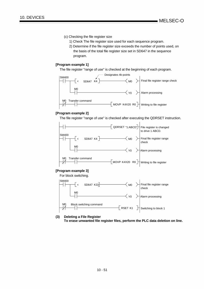
10 - 51
MELSEC-Q 10. DEVICES
(c) Checking the file register size
1) Check The file register size used for each sequence program.
2) Determine if the file register size exceeds the number of points used, on
the basis of the total file register size set in SD647 in the sequence
program.
[Program example 1]
The file register "range of use" is checked at the beginning of each program.
SM400
M0
Y0
M0 Transfer command
Final file register range check
M0
MOVP K4X20 R0
Alarm processing
Writing to file register
< SD647 K4
Designates 4k-points
[Program example 2] The file register "range of use" is checked after executing the QDRSET instruction.
SM400
M0
Y0
M0 Transfer command
Final file register range check
M0
MOVP K4X20 R0
Alarm processing
Writing to file register
< SD647 K4
QDRSET "1:ABCD" File register is changed to drive 1 ABCD.
[Program example 3] For block switching.
SM400
M0
Y0
M0 Block switching command
Final file register range check
M0
RSET K1
Alarm processing
Switching to block 1
< SD647 K33
(3) Deleting a File Register To erase unwanted file register files, perform the PLC data deletion on line.

10 - 52
MELSEC-Q 10. DEVICES
10.8 Nesting (N)
(1) Definition
Nesting devices are used to nest MC or MCR master control instructions when
programming operating conditions.
(2) Designation method with master control
The master control instructions are used to open and close the ladders' common
bus so that switching of ladders may be executed efficiently by the sequence
program. Nesting devices must be numbered in descending order (from N0 to
N7) of nested relation. For details on how to use master control, refer to the
QCPU(Q mode)/QnACPU Programming Manual (Common Instructions).
N0 nesting control range
N1 nesting control range
N2 nesting control range
Executed when conditions "A" and "B" are satisfied.
Executed when condition "A" is satisfied.
M15N0
B
C
A
M15N0MC
M16N1MC
N2MCR
N1MCR
M17N2MC
N0MC
M16N1
M17N2
Executed when condition "A", "B" and "C" are satisfied. MC2 to 7 are reset.
Executed when conditions "A" and "B" are satisfied.MC1 to 7 are reset.
Executed when condition "A" is satisfied.MC0 to 7 are reset.
Designated in ascending No. order
Designated in descending No. order
Executed regardless ofA, B, C condition statuses.
10 - 53
MELSEC-Q 10. DEVICES
10.9 Pointers
(1) Definition Pointer devices are used in jump instructions (CJ, SCJ, JUMP) or sub-routine call
instructions (CALL, ECALL).
A total of 4096 pointers can be used (total for all programs being executed).
(2) Pointer applications
(a) Pointers are used in jump instructions (CJ, SCJ, JMP) to designate jump
destinations and labels (jump destination beginning).
(b) Pointers are used in sub-routine CALL instructions (CALL, CALLP) to
designate the CALL destination and label (sub-routine beginning).
(3) Pointer types
There are 2 pointer types: "local pointers (Section 10.9.1)" which are used
independently in QCPU programs, and "common pointers (Section 10.9.1)"
which are used to call sub-routine programs from all programs executed in the
QCPU.
10.9.1 Local pointers
(1) Definition (a) Local pointers are pointers which can be used independently in QCPU
program jump instructions and sub-routine call instructions.
Local pointers cannot be used from other program jump instructions and sub-
routine CALL instructions.
Use an ECALL instruction to call a subroutine subprogram in a program file
that contains local pointers.
(b) The same pointer No. can be used in each of the programs. Program B
Same pointer is used.
Program A
P0P0
CALL P0
FEND
RET
END
CALL P0
FEND
RET
END
REMARK
For further information on jump instructions and sub-routine call instructions, see the
QCPU (Q Mode)/QnACPU Programming Manual (Common Instructions).

10 - 54
MELSEC-Q 10. DEVICES
(2) Number of local pointer points
Local pointers can be divided among all the programs stored in the program
memory.
The local pointer No. ranges from P0 to the highest No. of the local pointer in
use. (The QCPU's OS computes the number of points used.)
Even if only P99 is used in a program, for example, the number of points used
will be counted as 100 between P0 and P99.
Therefore, when local pointers are used at several programs, the pointer settings
should begin from P0.
If the total number of pointers (total for all programs) exceeds 4096 points, a
pointer configuration error (error code:4020) occurs.
P0 to P99 used in program
P100 to P199 used in program
Only P299 is used in program
P0 to P99 occupy 100 points
P0 to P199 occupy 200 points P0 to P299 occupy 300 points
If P0 is used, the number of occupied points is 1.
If P0 to P99 are used, the number of occupied points is 100.
Total of 600 points used.
Program A Program B Program C
If the local pointer points are used as follows, the total is 600 points.
Example
10.9.2 Common pointers
(1) Definition (a) Common pointers are used to call sub-routine programs from all programs
being executed in the QCPU. Program A
FEND
CALL P204
Program C
P204
P205
CALL P0
RET
RET
END
Program B
FEND
CALL P205
Label
(b) The same pointer No. cannot be used again as a label.
Such use will result in a pointer configuration error (error code:4021).
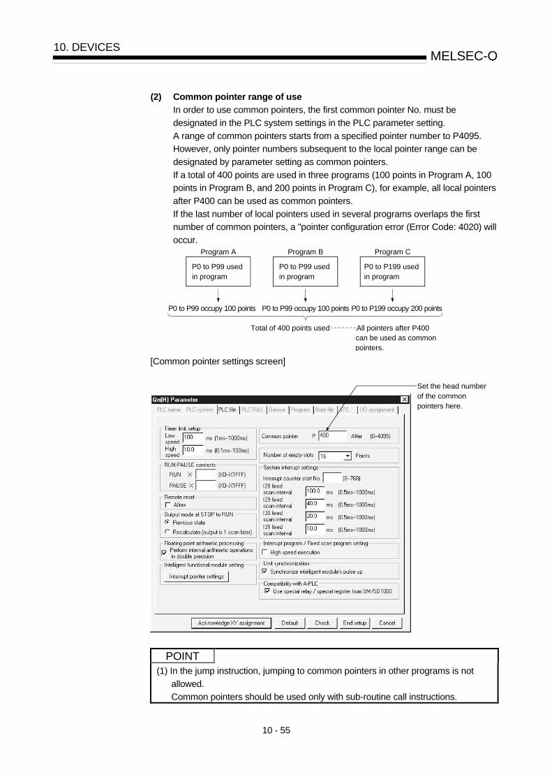
10 - 55
MELSEC-Q 10. DEVICES
(2) Common pointer range of use
In order to use common pointers, the first common pointer No. must be
designated in the PLC system settings in the PLC parameter setting.
A range of common pointers starts from a specified pointer number to P4095.
However, only pointer numbers subsequent to the local pointer range can be
designated by parameter setting as common pointers.
If a total of 400 points are used in three programs (100 points in Program A, 100
points in Program B, and 200 points in Program C), for example, all local pointers
after P400 can be used as common pointers.
If the last number of local pointers used in several programs overlaps the first
number of common pointers, a "pointer configuration error (Error Code: 4020) will
occur.
P0 to P99 usedin program
P0 to P99 usedin program
P0 to P199 usedin program
P0 to P99 occupy 100 points P0 to P99 occupy 100 points P0 to P199 occupy 200 points
Program A Program B Program C
Total of 400 points used All pointers after P400 can be used as common pointers.
[Common pointer settings screen]
Set the head number of the common pointers here.
POINT
(1) In the jump instruction, jumping to common pointers in other programs is not
allowed.
Common pointers should be used only with sub-routine call instructions.

10 - 56
MELSEC-Q 10. DEVICES
10.10 Interrupt Pointers (I)
(1) Definition (a) Interrupt pointers are used as labels at the beginning of interrupt programs.
Interrupt pointer (interrupt program label)
Interrupt program
IRET
I
(b) A total of 256 interrupt points (I0-I255) can be used (total for all programs
being executed).
(2) Interrupt pointer No. & interrupt factor
(a) As shown below, there are four types of interrupt factor.
• A1SI61 factor ......................... Interrupt input from the A1SI61 interruption
module.
• Sequence start generator ...... Interruption input from special function
module factor modules which can dictate an interrupt start to
the QCPU (A1SI61 excluded).
• Internal time factor ................. Fixed cycle interruption by QCPU's internal
timer.
• Error interruption .................... Interruption by an error that does not stop
sequence program operation.
• Intelligent-function .................. Interruption by an intelligent-function module.
module interrupt

10 - 57
MELSEC-Q 10. DEVICES
(b) A list of interrupt pointer Nos. and interrupt factors is given in Table 10.5
below. Table 10.5 List of Interrupt Pointer Nos. & Interrupt Factors
I No. Interrupt Factors Priority
Ranking I No. Interrupt factors
Priority Ranking
I0 1st point 237 I32*2 Errors that stop operation 1
I1 2nd point 238 I33 Vacant ——
I2 3rd point 239
I3 4th point 240
I4 5th point 241
I34
UNIT VERIFY ERR.
FUSE BREAK OFF
SP. UNIT ERROR
2
I5 6th point 242
I6 7th point 243
I7 8th point 244
I8 9th point 245
I35
OPERATION ERROR
SFCP OPE. ERROR
SFCP ECE. ERROR
EX. POWER OFF
3
I9 10th point 246
I10 11th point 247 I36
ICM. OPE ERROR
FILE OPE. ERROR 4
I11 12th point 248 I37 Vacant ——
I12 13th point 249 I38 PRG. TIME OVER 5
I13 14th point 250
I14 15th point 251 I39
Error factor*3*4,
CHK instruction execution
Anunciator detection 6
I15
A1SI61 interrupt
module factor
16th point 252
I16 1st point 224
I17 2nd point 225
I18 3rd point 226
I40 to
I49 —— Vacant ——
I19 4th point 227
I20 5th point 228
I21 6th point 229
I22 7th point 230
I23 8th point 231
I24 9th point 232
I25 10th point 234
I26 11th point 235
I27
Sequence start
generator module
factor*1
12th point 236
I28 100ms 256
I29 40ms 255
I30 20ms 254
I31
Internal timer factor
*2
10ms 253
I50 to
I255
Intelligent-function
module factor *5
Specifies which intelligent
function module is used
with parameters.
18 to 223
REMARK
1) *1 : 1st to 12th points are allocated in order, beginning from the sequence start generator module installed closest to the QCPU.
2) *2 :The internal times shown are the default setting times. These times can be designated in 0.5 ms units through a 0.5 ms to 1000 ms range by the GPPW(PLC system settings in the PLC parameter setting).
3) *3 :When an error interruption with "I32 (error that stops operation)" occurs, the QCPU is not stopped until I32 processing is completed.
4) *4 :Execution of error interruptions is prohibited for the interrupt pointer Nos. I32 to I39 when the power is turned on and during a QCPU reset. When using interrupt pointer Nos. I32 to I39, set the interruption permitted status by using the IMASK instruction.

10 - 58
MELSEC-Q 10. DEVICES
10.11 Other Devices
10.11.1 SFC block device (BL)
This device is used for checking if the block designated by the SFC program is active.
For details regarding the use of SFC block devices, refer to the QCPU(Q
mode)/QnACPU Programming Manual (SFC).
10.11.2 SFC transition device (TR)
This device is used for checking if a forced transition is designated for a specified
transition condition in a specified SFC program block.
For details regarding the use of SFC transition devices, refer to the QCPU(Q
mode)/QnACPU Programming Manual (SFC).
10.11.3 Network No. designation device (J)
(1) Definition The network No. designation device is used to designate the network No. in data
link instructions.
(2) Designating network No. designation device
The network No. designation device is designated in the data link instruction as
shown below.
JnJP.READ
Network No. designation device(n: network No.)
S1 S2 S3 D
Instruction nameNetwork No. designation instruction
REMARK
For details regarding data link instructions, refer to the MELSECNET/10H Network
System For Q Reference Manual.

10 - 59
MELSEC-Q 10. DEVICES
10.11.4 I/O No. designation device (U)
(1) Definition I/O No. designation devices are used with intelligent function module instruction
module instructions to designate I/O numbers.
(2) Designating the I/O No. designation device
I/O No. designation devices are designated with the intelligent function module
instructions as shown below.
UnGP.READ
I/O No. designation device(n: I/O No.)
S1 S2 S3 D
Instruction nameI/O No. designation instruction
REMARK
For details regarding intelligent function module instructions, refer to the
corresponding manual for the intelligent function module to be used.

10 - 60
MELSEC-Q 10. DEVICES
10.11.5 Macro instruction argument device (VD)
(1) Definition Macro instruction argument devices are used with ladders registered as macros. When a VD setting is designated for a ladder registered as a macro, conversion to the designated device occurs when the macro instruction is executed.
(2) Designating macro instruction argument devices Macro instruction argument devices are designated for those devices set as VD in ladders registered as macro instructions in macro registration at a peripheral device.* When using macro instructions in a sequence program, designate devices to correspond to the instruction argument devices used with the ladders registered as macros, in ascending order.
Transfer to VD2VD0MOV VD2VD0> VD1D0M.MAX D1 R0
Transfer to VD1
Transfer to VD0
VD1MOV VD2VD0<= VD1
Name of ladder registered as a macro
Actual sequence program executed at QCPU
Sequence program Ladder registered as a macro (registration name: MAX)
D0MOV R0D0> D1
D1MOV R0D0<= D1
REMARK
1) * : With the macro instruction argument device, VD0 to VD9 can be used in one ladder registered as a macro instruction.
2) The GPPW read mode provides an option to view a program in macro instruction format.(Choose "View" - "Macro Instruction format display" to view macro instructions.)
Change of macro instruction display

10 - 61
MELSEC-Q 10. DEVICES
10.12 Constants
10.12.1 Decimal constants (K)
(1) Definition Decimal constants are devices which designate decimal data in sequence
programs.
They are designated as "K "settings (e.g. K1234), and are stored in the QCPU
in binary (BIN) code.
See Section 4.8.1 for details regarding binary code.
(2) Designation range
The setting ranges for decimal constants are as follows:
• For word data (16 bits)............K-32768 to K32767
• For 2-word data (32 bits) ........K-2147483648 to K2147483647
10.12.2 Hexadecimal constants (H)
(1) Definition Hexadecimal constants are devices which designate hexadecimal or BCD data in
sequence programs.
(For BCD data designations, 0 to 9 digit designations are used.)
Hexadecimal constants are designated as "H " settings (e.g. H1234).
See Section 4.8.3 for details regarding hexadecimal code.
(2) Designation range
The setting ranges for hexadecimal constants are as follows:
• For word data (16 bits)............H0 to HFFFF (H0 to H9999 for BCD)
• For 2-word data (32 bits) ........H0 to HFFFFFFFF (H0 to H99999999 for BCD)
10 - 62
MELSEC-Q 10. DEVICES
10.12.3 Real numbers (E)
(1) Definition Real numbers are devices which designate real numbers in the sequence
program.
Real numbers are designated as "E "settings (e.g. E1.234).
X1E1.234 D0EMOVP
See Section 4.8.4 for details regarding real numbers. (2) Designation range
The setting range for real numbers is -1.0 2128 to -1.0x2-126, 0 and 1.0 2-126 to
1.0 2128.
(3) Designation method
Real numbers can be designated in sequence programs by a "normal
expression" or an "exponential expression".
• Normal expression............ The specified value is designated as it is.
For example, 10.2345 becomes E10.2345.
• Exponential expression .... The specified value is multiplied by a " 10n"exponent.
For example, 1234 becomes E1.234 + 3.*
REMARK
1) *:The "+3" in the above example represents a 10nvalue (103).
10.12.4 Character string ( " )
(1) Definition Character string constants are devices used to designate character strings in
sequence programs.
They are designated by quotation marks (e.g. "ABCD1234").
(2) Usable characters
All ASCII code characters can be used in character strings.
The QCPU is sensitive to uppercase and lowercase characters.
(3) Number of designated characters
Character strings extend from the designated character to the NUL code (00H).
You can use up to 32 characters for a character string in an instruction such as
$MOV.

10 - 63
MELSEC-Q 10. DEVICES
10.13 Convenient Uses for Devices
When executing multiple programs in the QCPU, local devices among the internal user
devices can be designated to execute each of the programs in an independent
manner.
Moreover, the device initial settings can be used to designate device and intelligent
function module/special function module data settings without using a program.
10.13.1 Global devices & local devices
A number of programs can be stored and executed in the QCPU.
QCPU devices which can be shared by all the programs are "global devices", and
those used independently by each of the programs are "local devices".
(1) Global devices
(a) Global devices are devices which can be shared by all the programs being
executed in the QCPU. Global devices are stored in the QCPU's device
memory, with all programs using the same devices.
Y12
M0
Program A
Y11
M0
Program B
M0 ON/OFF data
Device memory
Internal relay
ON/OFFM0
M0 ON/OFF data
Global devices are shared by all programs being executed.
QCPU
(b) When executing multiple programs, the "shared range" for all programs, and
the "independent range" for each program must be designated in advance.
Example: Internal relay
M0 Shared by all programs
Used in program A
Used in program B
Used in program C
The "range of use" must be designated for each program.

10 - 64
MELSEC-Q 10. DEVICES
(2) Local devices
(a) Local devices are devices which are used independently by the programs.
The use of local devices permits programming of multiple "independent
execution" programs without regard to other programs.
However, local devices data can be stored in the standard RAM and the
memory card.
Y12
M7000
Program A
Y11
M7000
Program B
M7000 ON/OFF data
M7000 ON/OFF data
If local devices are designated as the devices which follow M7000, they can be used independently in programs executed after M7000.
QCPU
Internal relay
ON/OFFM7000
For program A
Internal relay
ON/OFFM7000
For program B
Memory card
(b) Five device types can be used as local devices: internal relays (M), edge
relays (V), timers (T, ST), counters (C), and data registers (D).
(c) When local devices are used, an exchange occurs between the local device
file data stored in the standard RAM or memory card, and the data in the
QCPU's device area.
The scan time is therefore extended by this data exchange time.
Local device
Program A Program B Program C
Local device Local device
Reset Saved Reset Saved Reset
Sequence program
For program A
For program B
For program C
For program A
For program B
For program C
For program A
For program B
For program C
REMARK
1) * : See Section 10.1.2 (item 2) for details regarding the "number of words" for
local devices.

10 - 65
MELSEC-Q 10. DEVICES
(d) Local device designation
1) In order to use the above devices as local devices, a local device range of
use setting must be designated in the device settings in the PLC parameter
setting.
Note that the range designated for local devices applies in all programs,
and cannot be changed for individual programs.
For example, if the local device range is designated as M0 to M100, this
range will be used for local devices in all programs.
Local device
Program A
Local device
Program B
Local device
Program C
This range becomes the local device range for all programs.
M0
M100
2) When local device settings are designated, the drive and file name where
the local device data is to be stored must be designated in the PLC file
settings in the PLC parameter setting.
3) To write data from the GPPW onto the QCPU, use the PLC File sheet of
the PLC Parameter dialog box to specify whether to use a local device. If a
local device is not specified, the local devices used for previously-executed
programs are selected. This does not require replacing local devices in a
memory card with the device memory of the QCPU. If local devices are not
used for Program B while executing Programs A, B, and C, the local
devices are used as shown below.
Local device
Program A Program C Program A
Local device Local device
Reset Saved Reset Saved Reset
Sequence program
For program A
For program B
For program C
Forprogram A
For program B
For program C
For program A
For program B
For program C
Program B Program B
Used local device of program A
POINT
(1) Unless specifically designated as "local devices", all devices are global devices.
(e) Using local devices used by the file where a sub-routine program is stored
It is possible to use local devices that are used by the file where a sub-routine
program is stored when executing a sub-routine program.
Whether or not such local devices are used is set by special relay "SM776"
ON/OFF setting.

10 - 66
MELSEC-Q 10. DEVICES
1) Switching over local devices by setting ON/OFF for a special relay (SM776)
SM776
OFF Executes calculation by the local devices that are used by the file where the sub-routine program was called
ON Executes calculation by the local devices that are used by the file where the sub-routine program is stored.
[Operation at "SM776 : OFF"]
CALL P100X0
INCP D0X2
END
Local devices used bythe file name: ABC
File name: ABC
Local devices used bythe file name: DEF
File name: DEF (Standby program)
RET
P100
Subroutine program
Read/write of thelocal devices
Execution of the subroutine program
[Operation at "SM776 : ON"]
CALL P100X0
INCP D0X2
END
Local devices used by the file name: ABC
File name: ABC
Local devices used by the file name: DEF
File name: DEF (Standby program)
RET
P100
Subroutine programRead/write of the
local devices
Execution of the subroutine program
2) Cautions
• If SM776 is ON, the local device data is read when the sub-routine
program is called and the local device data is saved after the execution of
the RET instruction. Accordingly, scan time is elongated by the time as
shown below when a sub-routine program is executed once with the
setting of "SM776: ON". (See Section 10.13.1)
• ON/OFF setting of SM776 is possible in unit of CPU.
Setting in unit of file is not possible.
• If the ON/OFF setting of SM776 is changed while a sequence program is
executed, the control is made according to the information after change.
REMARK
For details on SM776, see Appendix 1 of this manual.

10 - 67
MELSEC-Q 10. DEVICES
(f) Using local devices when executing an interrupt/fixed scan execution type
program
It is possible to use local devices that are used by the file where an
interrupt/fixed scan execution type program is stored when executing an
interrupt/fixed scan execution type program.
Whether or not such local devices are used is set by special relay "SM777"
ON/OFF setting.
1) Switching over local devices by setting ON/OFF for a special relay (SM777)
SM777
OFF Executes calculation by the local devices that are used by the file which was executed before the execution of the interrupt/fixed scan execution type program.
ON Executes calculation by the local devices that are used by the file where the interrupt/fixed scan execution type program is stored.
[Operation at "SM777 : OFF"]
DECP D1X0
INCP D0X2
END
Local devices used by the file name: ABC
File name: ABC
Local devices used by the file name: DEF
File name: DEF (Standby program)
IRET
I0
Interrupt program
Occurrenceof interrupt Execution of the
interrupt program
Read/write of the local devices
[Operation at "SM777 : ON"]
DECP D1X0
INCP D0X2
END
Local devices used bythe file name: ABC
File name: ABC
Local devices used bythe file name: DEF
File name: DEF(Standby program)
IRET
I0
Interruptprogram
Occurrence of interrupt Execution of the
interrupt program
Read/write of thelocal devices
REMARK
For details on SM777, see Appendix 1 of this manual.

10 - 68
MELSEC-Q 10. DEVICES
2) Cautions
• If SM777 is ON, the local device data is read before the interrupt/fixed
scan execution type program is executed and the local device data is
saved after the execution of the IRET instruction.
Accordingly, scan time increases when an interrupt/fixed scan execution
type program is executed once with the setting of "SM777: ON". (See
Section 10.13.1)
• ON/OFF setting of SM777 is possible in unit of CPU.
Setting in unit of file is not possible.
• If the ON/OFF setting of SM777 is changed while a sequence program is
executed, the control is made according to the information after change.
(g) Clearing the Local Device Data
The local device data is cleared in the following cases where:
1) The QCPU is turned on or reset.
2) The QCPU enters from the STOP status into the RUN status.
The local device data cannot be cleared by operating from the GPPW. To
clear the local device data, follow the above-listed steps 1) and 2).

10 - 69
MELSEC-Q 10. DEVICES
10.13.2 Device initial values
(1) Definition (a) Using device initial setting values, the data used for a program can be stored
in device or intelligent function module buffer memories without using a data
setting program.
The use of device initial values provides a shortcut to specify device data in a
program without using a device data setting program (initial program).
[Data setting by initial processing program]
Device memoryPower supply ON/STOP to RUN
SM402
MOV H100 D0
MOV H2020 D1
Device memory
Power supply ON/STOP to RUN
Device initial value
(b) In order to use the device initial values, the device initial data must be created
in advance at the GPPW device, and this data must be stored as a device
initial value file in the QCPU's program memory, standard RAM or memory
card.
At power ON, or on switching from STOP to RUN, the QCPU writes the data
from the device initial value file to the specified device or intelligent function
module buffer memory.
GPPW
"Device initial value range" setting
"Device initial value data" setting
Program memory, Standard ROM, Memory card
Device initial value file
Device initial value writing
(Power supply ON/STOP to RUN)
Designated device
Intelligent function module
QCPU
Device initial value writing

10 - 70
MELSEC-Q 10. DEVICES
(c) Device initial values can be used at the following devices:
1) Timer present value (T) 7) Special link register (SW)
2) Retentive timer present value (ST) 8) File register (R0 to R32767)
3) Counter present value (C) 9) Intelligent function module device
4) Data register (D) (U \G )
5) Special register (SD) 10) Link direct device (J \W ,
6) Link register (W) J \SW )
(2) Procedure for using device initial values
(a) Designate the device initial value range settings in the device mode, in the
device initial value setting screen.
(b) Designate the device initial value data settings in the device mode screen.
[Device initialization range setting screen]
[Device mode screen]
(c) In the PLC file settings in the PLC parameter setting, designate the name of
the file where the device initial value data is to be stored.
[PLC file screen]
(d) Write the device initial value data and parameter settings to the QCPU.

10 - 71
MELSEC-Q 10. DEVICES
(3) Precautions for the use of device initial values
(a) In cases where both device initial value data and latch range data are
present, the device initial value data takes precedence.
Therefore, the latch range data is overwritten by device initial value data at
power ON.
(b) Device initial values cannot be used in areas where no setting is made for
switching from STOP to RUN (for data that is changed by a program at power
ON). Create a program to specify a device by using the MOV instruction in the
main routine program. Use the TO instruction to write data onto the buffer
memory of the intelligent function unit.
REMARK
For details regarding the setting procedures for the "device initial value range",
"device initial value data" items, and for writing the device initial values to the QCPU,
refer to the GPP Function Software Package Operating Manual.

10 - 72
MELSEC-Q 10. DEVICES
MEMO
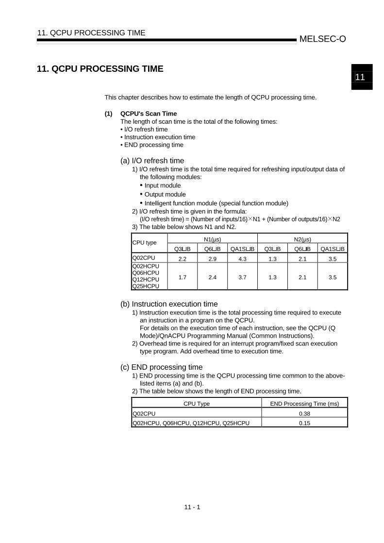
11 - 1
MELSEC-Q 11. QCPU PROCESSING TIME
11
11. QCPU PROCESSING TIME
This chapter describes how to estimate the length of QCPU processing time.
(1) QCPU's Scan Time
The length of scan time is the total of the following times: • I/O refresh time • Instruction execution time • END processing time
(a) I/O refresh time
1) I/O refresh time is the total time required for refreshing input/output data of the following modules: • Input module • Output module • Intelligent function module (special function module)
2) I/O refresh time is given in the formula: (I/O refresh time) = (Number of inputs/16) N1 + (Number of outputs/16) N2
3) The table below shows N1 and N2.
N1(µs) N2(µs) CPU type Q3 B Q6 B QA1S B Q3 B Q6 B QA1S B
Q02CPU 2.2 2.9 4.3 1.3 2.1 3.5 Q02HCPU Q06HCPU Q12HCPU Q25HCPU
1.7 2.4 3.7 1.3 2.1 3.5
(b) Instruction execution time
1) Instruction execution time is the total processing time required to execute an instruction in a program on the QCPU. For details on the execution time of each instruction, see the QCPU (Q Mode)/QnACPU Programming Manual (Common Instructions).
2) Overhead time is required for an interrupt program/fixed scan execution type program. Add overhead time to execution time.
(c) END processing time
1) END processing time is the QCPU processing time common to the above-listed items (a) and (b).
2) The table below shows the length of END processing time.
CPU Type END Processing Time (ms)
Q02CPU 0.38
Q02HCPU, Q06HCPU, Q12HCPU, Q25HCPU 0.15

11 - 2
MELSEC-Q 11. QCPU PROCESSING TIME
(2) Factors Responsible for Extended Scan Time
The following functions increase the length of scan time. When using any of the
following functions, add a value of extended time to values obtained from items
(a), (b) and (c).
• MELSECNET/10H refresh
• CC-Link automatic refresh
• Sampling trace
• GPPW monitoring
• Local devices
• Execution of multiple programs
• Installation/removal of a memory card
• File register with the same filename as a program.
(a) MELSECNET/10H refresh
MELSECNET/10H refresh requires additional processing time to refresh
data between the QCPU and the MELSECNET/10H network module. For
details on MELSECNET/10H refresh time, see the MELSECNET/10H
Network System For Q Reference Manual.
(b) CC-Link automatic refresh
CC-Link automatic refresh requires additional processing time to refresh
data between the QCPU and the CC-Link's master local module. When a
CC-Link master local module is installed, scan time is extended for some
time because refresh processing is performed by default. The table below
shows CC-Link automatic refresh time.
Processing Time (ms) CPU Type
Mater Station Local Station
Q02CPU 1.10 2.1
Q02HCPU, Q06HCPU, Q12HCPU, Q25HCPU 0.80 1.5
When a CC-Link master local module is installed, extended scan time can
be shortened by adjusting a CC-Link setting to a system setting. For details
on CC-Link automatic refresh time, see the QJ61BT11 Type CC-Link
System Master Local Module Users Manual - Details.
(c) Sampling trace time
Sampling trace requires additional processing time. When sampling trace
data is specified to execute the sampling trace function, add the sampling
trace time to the total processing time.
The table below shows the length of processing time required when
sampling trace data is specified to assign 50 internal relay points for bit
devices and 50 data register points for word deices.
CPU Type Processing Time (ms)
Q02CPU 0.24
Q02HCPU, Q06HCPU, Q12HCPU, Q25HCPU 0.12
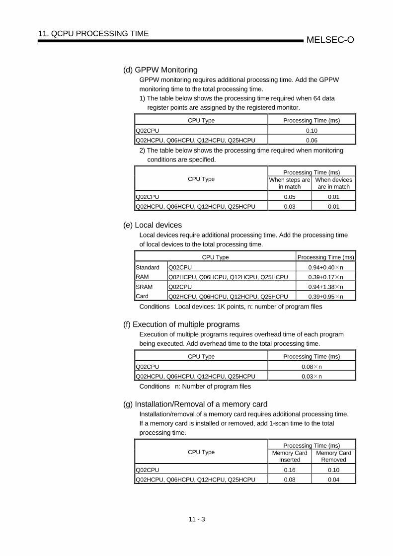
11 - 3
MELSEC-Q 11. QCPU PROCESSING TIME
(d) GPPW Monitoring
GPPW monitoring requires additional processing time. Add the GPPW
monitoring time to the total processing time.
1) The table below shows the processing time required when 64 data
register points are assigned by the registered monitor.
CPU Type Processing Time (ms)
Q02CPU 0.10
Q02HCPU, Q06HCPU, Q12HCPU, Q25HCPU 0.06
2) The table below shows the processing time required when monitoring
conditions are specified.
Processing Time (ms) CPU Type When steps are
in match When devices are in match
Q02CPU 0.05 0.01
Q02HCPU, Q06HCPU, Q12HCPU, Q25HCPU 0.03 0.01
(e) Local devices
Local devices require additional processing time. Add the processing time
of local devices to the total processing time.
CPU Type Processing Time (ms)
Q02CPU 0.94+0.40 n Standard
RAM Q02HCPU, Q06HCPU, Q12HCPU, Q25HCPU 0.39+0.17 n
Q02CPU 0.94+1.38 n SRAM
Card Q02HCPU, Q06HCPU, Q12HCPU, Q25HCPU 0.39+0.95 n
Conditions Local devices: 1K points, n: number of program files
(f) Execution of multiple programs
Execution of multiple programs requires overhead time of each program
being executed. Add overhead time to the total processing time.
CPU Type Processing Time (ms)
Q02CPU 0.08 n
Q02HCPU, Q06HCPU, Q12HCPU, Q25HCPU 0.03 n
Conditions n: Number of program files
(g) Installation/Removal of a memory card
Installation/removal of a memory card requires additional processing time.
If a memory card is installed or removed, add 1-scan time to the total
processing time.
Processing Time (ms) CPU Type Memory Card
Inserted Memory Card
Removed
Q02CPU 0.16 0.10
Q02HCPU, Q06HCPU, Q12HCPU, Q25HCPU 0.08 0.04
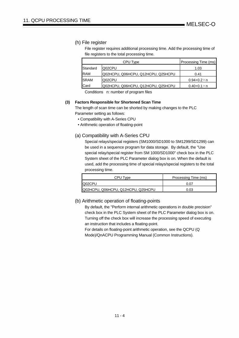
11 - 4
MELSEC-Q 11. QCPU PROCESSING TIME
(h) File register
File register requires additional processing time. Add the processing time of
file registers to the total processing time.
CPU Type Processing Time (ms)
Q02CPU 1.03 Standard
RAM Q02HCPU, Q06HCPU, Q12HCPU, Q25HCPU 0.41
Q02CPU 0.94+0.2 n SRAM
Card Q02HCPU, Q06HCPU, Q12HCPU, Q25HCPU 0.40+0.1 n
Conditions n: number of program files
(3) Factors Responsible for Shortened Scan Time
The length of scan time can be shorted by making changes to the PLC
Parameter setting as follows:
• Compatibility with A-Series CPU
• Arithmetic operation of floating-point
(a) Compatibility with A-Series CPU
Special relays/special registers (SM1000/SD1000 to SM1299/SD1299) can
be used in a sequence program for data storage. By default, the "Use
special relay/special register from SM 1000/SD1000" check box in the PLC
System sheet of the PLC Parameter dialog box is on. When the default is
used, add the processing time of special relays/special registers to the total
processing time.
CPU Type Processing Time (ms)
Q02CPU 0.07
Q02HCPU, Q06HCPU, Q12HCPU, Q25HCPU 0.03
(b) Arithmetic operation of floating-points
By default, the "Perform internal arithmetic operations in double precision"
check box in the PLC System sheet of the PLC Parameter dialog box is on.
Turning off the check box will increase the processing speed of executing
an instruction that includes a floating-point.
For details on floating-point arithmetic operation, see the QCPU (Q
Mode)/QnACPU Programming Manual (Common Instructions).

12 - 1
MELSEC-Q 12. PROCEDURE FOR WRITING PROGRAMS TO QCPU
12
12. PROCEDURE FOR WRITING PROGRAMS TO QCPU
This chapter describes the procedure for writing programs created at the GPPW to the
QCPU.
12.1 Writing Procedure For 1 Program
This section describes the procedure for writing one program to the QCPU and
executing it.
12.1.1 Items to consider when creating one program
In order to create a program, the program size, number of device points used, and the
program file name, etc., must be set in advance.
(1) Program size considerations
Check that CPU's program capacity is adequate for storing the program and
parameter data.
The program capacities of the CPUs are shown below:
• Q02CPU : 28 k steps
• Q02HCPU : 28 k steps
• Q06HCPU : 60 k steps
• Q12HCPU : 124 k steps
• Q25HCPU : 252 k steps
If the CPU capacity is only adequate for the program, the parameter data should
be stored in the standard ROM/memory card.
(2) Designating a program file name
The file name of the program to be stored in the QCPU must be designated.
This file name is used when writing the program and parameters from the GPPW
to the QCPU, and when designating the program to be executed in the QCPU.
See Chapter 6 for details regarding file names.
(3) Designating devices
The number of devices required for the program must be determined.
See Chapter 10 for details regarding devices which can be used in the QCPU.
(4) Device initial value setting
Designate whether or not the device initial value settings are to be used in the
QCPU devices and intelligent function modules.
See Section 10.13.2 for details regarding device initial values.

12 - 2
MELSEC-Q 12. PROCEDURE FOR WRITING PROGRAMS TO QCPU
12.1.2 Procedure for writing programs to the QCPU
The procedure for writing programs and parameters created at the GPPW to the
QCPU standard ROM is shown below.
In order to write programs and parameters to the QCPU standard ROM, the valid
parameters settings must be designated by the QCPU DIP switches (SYS 1), and the
boot settings must be designated in the PLC parameter mode.
For details regarding QCPU DIP switches, refer to the QCPU(Q mode) User's
Manual(Hardware Design and Maintenance & Inspection).
When writing programs and parameters to the QCPU program memory, the steps
indicated by asterisks (*) below are not required.
Procedural steps shown in boxes are performed at the GPPW, and those shown in
boxes are performed in the QCPU.
Start
Refer to the GPP functionSoftware package Operating Manual.
Start the GPPW
Change the number of devicepoints at the device settingitem in the PLC parameter.
Mode selection screenis displayed.
Change thenumber of device
points?
Create the program which isto be executed in the OCPU.
1)
YES
NORefer to Section 10.1.2.

12 - 3
MELSEC-Q 12. PROCEDURE FOR WRITING PROGRAMS TO QCPU
Use the deviceinitial value?
1)
YES
NORefer to Section 10.13.2.
Right-click on the devicememory and make a dataentry for device initial values.
Right-click on a device initialvalue and select "Add" to spe-cify a device initial value range.
Select "Use device memory"from the device memoryregistration setting and specifythe device to be used.
In the boot file setting item inthe PLC parameter, designatethe file name of parameter andprogram to be read from thestandard ROM.
In the program settings in the PLCparameter, designate the nameof the program to be executed,and its execution condition.
Connect the GPPW to the QCPU.
Set the QCPU's RUN/STOPkey to the STOP position,then switch the power ON.
In the GPPW online mode,select the program memory,and use the PLC memorybatch operation to format theprogram memory.
2)
*
In the PLC file setting in thePLC parameter, designate thename of file to be used for thedesignated device initial values.
*
ERROR LED switches ON.

12 - 4
MELSEC-Q 12. PROCEDURE FOR WRITING PROGRAMS TO QCPU
In the GPPW online mode,select the standard ROM, andwrite the parameter data andcreated program.
2)
Use the QCPU's RESET/L.CLRswitch to execute a reset.
QCPU's "BOOT" LEDswitches ON.
End
If a boot file setting is not made(or when writing parameters orprograms onto the program memory),the "BOOT" LED does not light up.

12 - 5
MELSEC-Q 12. PROCEDURE FOR WRITING PROGRAMS TO QCPU
12.2 Procedure For Multiple Programs
This section describes the procedure for writing multiple programs split up according to function, process, designer to the QCPU and executing them.
12.2.1 Items to consider when creating multiple programs
To create multiple programs, it is necessary to set in advance the size of each program, the device used, and the program file name, etc. (1) Program size considerations
Set the program capacity within the range of the QCPU program capacity. The program capacities of the QCPU's are shown below: • Q02CPU : 28 k steps • Q02HCPU : 28 k steps • Q06HCPU : 60 k steps • Q12HCPU : 124 k steps • Q25HCPU : 252 k steps Decide whether the parameters are to be stored in the program memory, the standard ROM, or the memory card. If they are to be stored in the program memory/the standard ROM, the area available for the program will be the capacity shown above, minus the parameter data size.
(2) Designating a program file name Designate the file name of the program to be stored in the QCPU. This file name is used when writing the program and parameters from the GPPW to the QCPU, and when designating the program to be executed in the QCPU. See Chapter 6 for details regarding file names.
(3) Designating the program execution conditions In order to execute multiple programs in the QCPU, execution conditions must be designated for each program. Execution is impossible for programs without file name and execution condition settings. See Section 4.2 for details regarding execution conditions.
(4) Designating devices (a) Designate the number of device points used in each program, and the
number of device points which are shared by all programs. See Chapter 10 for details regarding devices which can be used in the QCPU.
(b) Designate whether or not the internal relays, edge relays, timers, counters, and data registers of each program are to be designated as local devices. See Section 10.13.1 for details regarding local devices.
(c) When creating sub-routine programs, designate whether or not common pointers are to be used. See Section 10.9.2 for details regarding common pointers.
(5) Device initial value setting
Designate whether or not the device initial value settings are to be used for the QCPU devices and intelligent function modules. See Section 10.13.2 for details regarding device initial values.

12 - 6
MELSEC-Q 12. PROCEDURE FOR WRITING PROGRAMS TO QCPU
12.2.2 Procedure for writing programs to the QCPU
The procedure for writing programs and parameters created at the GPPW to the
memory card installed in the QCPU memory card interface is shown below.
In order to write programs and parameters to the QCPU memory card, the memory
card must be installed, the valid parameters drive settings must be designated by the
QCPU DIP switches (SW 1), and the boot settings for the PLC parameters must be
designated by the GPPW.
For details regarding QCPU DIP switches, refer to the QCPU (Q mode) User's Manual
(Hardware Design and Maintenance & Inspection).
When writing programs and parameters to the QCPU program memory, the steps
indicated by asterisks (*) below are not required.
Procedural steps shown in boxes are performed at the GPPW, and those shown in
boxes are performed at the QCPU.
Start
Refer to the GPP functionSoftware package Operating Manual.
Start the GPPW.
Change the number of devicepoints at the device settingitem in the PLC parameter.
Mode selection screenis displayed.
Change thenumber of device
points?
Create the program which isto be executed in the OCPU.
1)
YES
NORefer to Section 10.1.2.

12 - 7
MELSEC-Q 12. PROCEDURE FOR WRITING PROGRAMS TO QCPU
Use the deviceinitial value?
1)
YES
NO
Right-click on the devicememory and make a dataentry for device initial values.
Right-click on a device initialvalue and select "Add" to specifya device initial value range.
Select "Use device memory"from the device memory regi-stration setting and specifythe device to be used.
2)
Designate localdevices?
YES
NO
In the device setting item in thePLC parameter, designate thename of the local device range.
In the PLC file setting item inthe PLC parameter, designatethe name of the local device file.
Use the commonpointers?
YES
NO
In the PLC system setting itemin the PLC parameter, desig-nate the first pointer No.
Refer to Section 10.13.2.
In the PLC file setting in thePLC parameter, designate thename of file to be used for thedesignated device initial values.
Refer to Section 10.13.1.
Refer to Section 10.9.2.
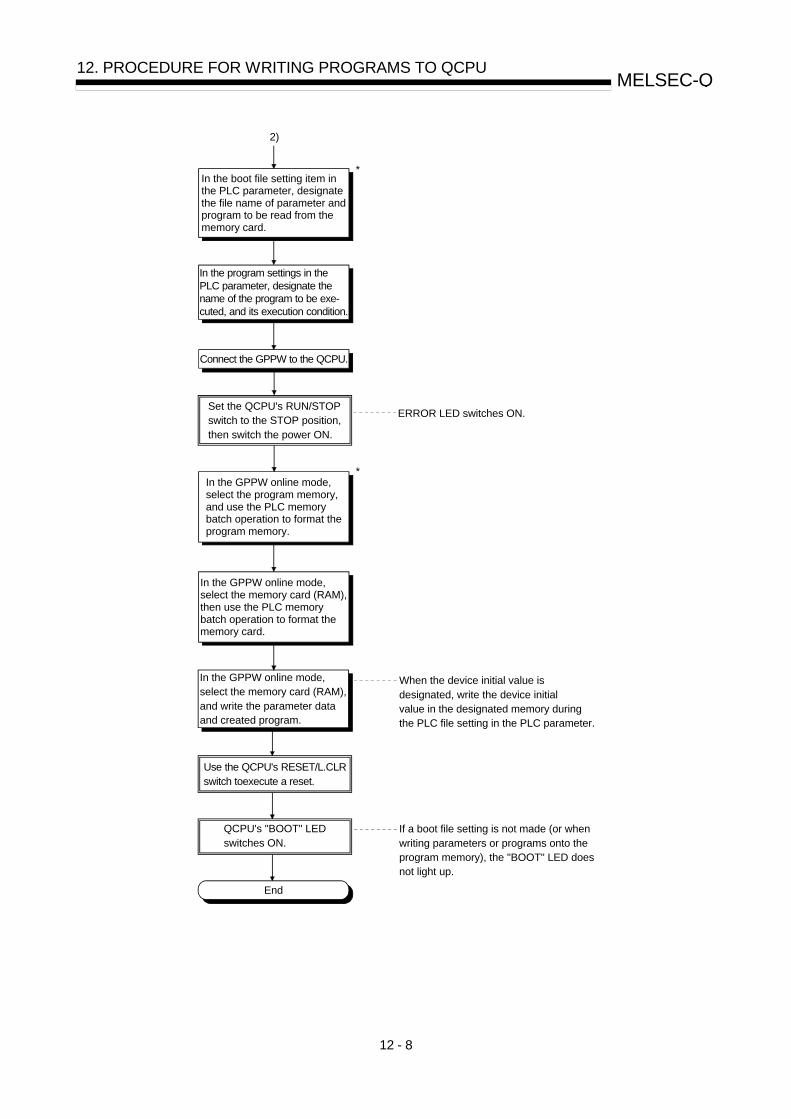
12 - 8
MELSEC-Q 12. PROCEDURE FOR WRITING PROGRAMS TO QCPU
2)
In the GPPW online mode,select the memory card (RAM),and write the parameter dataand created program.
Use the QCPU's RESET/L.CLRswitch toexecute a reset.
QCPU's "BOOT" LEDswitches ON.
End
In the boot file setting item inthe PLC parameter, designatethe file name of parameter andprogram to be read from thememory card.
In the program settings in thePLC parameter, designate thename of the program to be exe-cuted, and its execution condition.
Connect the GPPW to the QCPU.
Set the QCPU's RUN/STOPswitch to the STOP position,then switch the power ON.
*
In the GPPW online mode,select the memory card (RAM),then use the PLC memorybatch operation to format thememory card.
ERROR LED switches ON.
In the GPPW online mode,select the program memory,and use the PLC memorybatch operation to format theprogram memory.
*
When the device initial value isdesignated, write the device initialvalue in the designated memory duringthe PLC file setting in the PLC parameter.
If a boot file setting is not made (or whenwriting parameters or programs onto theprogram memory), the "BOOT" LED doesnot light up.
App - 1
MELSEC-Q APPENDICES
App.
APPENDICES
APPENDIX 1 Special Relay List
Special relays, SM, are internal relays whose applications are fixed in the
programmable controller.
For this reason, they cannot be used by sequence programs in the same way as the
normal internal relays.
However, they can be turned ON or OFF as needed in order to control the QnACPU.
The headings in the table that follows have the following meanings. Item Function of Item
Number • Indicates the number of the special relay.
Name • Indicates the name of the special relay.
Meaning • Indicates the nature of the special relay.
Explanation • Contains detailed information about the nature of the special relay.
Set by (When set)
• Indicates whether the relay is set by the system or user, and, if it is set by the system, when
setting is performed.
<Set by>
S : Set by system
U : Set by user (in sequence program or test operation at a peripheral device)
S/U : Set by both system and user
<When set> indicated only if setting is done by system.
Each END : Set during each END processing
Initial : Set only during initial processing
(when power supply is turned ON, or when going from STOP to
RUN)
Status change : Set only when there is a change in status
Error : Set when error is generated
Instruction execution : Set when instruction is executed
Request : Set only when there is a user request
(through SM, etc.)
Corresponding ACPU
M9
• Indicates special relay M9 / corresponding to the ACPU.
(Change and notation when there has been a change in contents)
• Items indicated as "New" have been newly added for Q/QnACPU
Corresponding CPU
• Indicates the corresponding CPU type name.
: Can be applied to all types of CPU
QCPU: Can be applied to Q-series CPU
QnA: Can be applied to QnA series and Q2ASCPU series
Each CPU type name: Can be applied only to the specific CPU. (e.g. Q4ARCPU, Q3ACPU)
For details on the following items, see these manuals:
• Networks • MELSECNET/10H Network System Reference Manual for Q
• MELSECNET/10 Network System Reference Manual for QnA
• SFC QCPU/QnACPU Programming Manual (SFC)
POINT
(1) SM1200 to SM1255 are used for QnACPU.
These relays are vacant with QCPU.
(2) Special relays SM1500 and later are dedicated for Q4ARCPU.
App - 2
MELSEC-Q APPENDICES
Special Relay List
(1) Diagnostic Information
Number Name Meaning Explanation Set by (When Set)
Corresponding ACPU
M9
Applicable CPU
SM0 Diagnostic errors OFF : No error ON : Error
• ON if diagnosis results show error occurrence (Includes external diagnosis)
• Stays ON subsequently even if normal operations restored
S (Error) New
SM1 Self-diagnostic error
OFF : No self-diagnosis errors
ON : Self-diagnosis
• Comes ON when an error occurs as a result of self-diagnosis.
• Stays ON subsequently even if normal operations restored
S (Error) M9008
SM5 Error common information
OFF : No error common information
ON : Error common information
• When SM0 is ON, ON if there is error common information
S (Error) New
SM16 Error individual information
OFF : No error common information
ON : Error common information
• When SM0 is ON, ON if there is error individual information
S (Error) New
SM50 Error reset OFF ON : Error reset • Conducts error reset operation • See section 11.3 for further information
U New
SM51 Battery low latch OFF : Normal ON : Battery low
• ON if battery voltage at CPU or memory card drops below rated value. Stays ON subsequently even after normal operation is restored
• Synchronous with BAT. ALARM LED
S (Error) M9007
SM52 Battery low OFF : Normal ON : Battery low
• Same as SM51, but goes OFF subsequently when battery voltage returns to normal.
S (Error) M9006
SM53 AC DOWN detection
OFF : AC DOWN not detected
ON : AC DOWN detected
• Comes ON when there is a momentary power interruption not exceeding 20 ms; reset by turning the power OFF then ON again.
S (Error) M9005
SM54 MINI link errors OFF : Normal ON : Error
• Goes ON if MINI (S3) link error is detected at even one of the installed AJ71PT32 (S3) modules. Stays ON subsequently even after normal operation is restored.
S (Error) M9004 QnA
SM56 Operation Errors OFF : Normal ON : Operation error
• ON when operation error is generated • Stays ON subsequently even if normal operations
restored S (Error) M9011
SM60 Blown fuse detection
OFF : Normal ON : Module with blown fuse
• Comes ON even if there is only one output module with a blown fuse, and remains ON even after return to normal
• Blown fuse state is checked even for remote I/O station output modules.
S (Error) M9000
SM61 I/O module Verification error
OFF : Normal ON : Error
• Comes ON if there is a discrepancy between the actual I/O modules and the registered information when the power is turned on
• I/O module verification is also conducted for remote I/O station modules.
S (Error) M9002
SM62 Annunciator detection
OFF : Not detected ON : Detected
• Goes ON if even one annunciator F goes ON. S
(Instruction execution)
M9009
SM80 CHK detection OFF : Not detected ON : Detected
• Goes ON if error is detected by CHK instruction. • Stays ON subsequently even after normal operation is
restored.
S (Instruction execution)
New
SM90 Corresponds to SD90 M9108
SM91 Corresponds to SD91 M9109
SM92 Corresponds to SD92 M9110
SM93 Corresponds to SD93 M9111
SM94 Corresponds to SD94 M9112
SM95 Corresponds to SD95 M9113
SM96 Corresponds to SD96 M9114
SM97 Corresponds to SD97 New
SM98 Corresponds to SD98 New
SM99
Startup of watchdog timer for step transition (Enabled only when SFC program exists)
OFF : Not started (watchdog timer reset)
ON : Started (watchdog timer started)
Corresponds to SD99
• Goes ON when measurement of step transition watchdog timer is commenced.
• Resets watchdog timer when it goes OFF.
U
New
SM120 Detection of
external power
supply OFF
OFF : Normal
ON : There is a module
whose external power
supply is OFF.
• Goes ON when at least one module is in the status
where the external power supply is OFF. Stays ON even
after normal operation is restored.
Applicable only for Q-series module. (For future use)
S (Error) New QCPU

App - 3
MELSEC-Q APPENDICES
Special Relay List
(2) System information
Number Name Meaning Explanation Set by (When Set)
Corresponding ACPU
M9
Applicable CPU
SM202 LED off command
OFF ON : LED off • At change from OFF to ON, the LEDs corresponding to
the individual bits at SD202 go off U New
SM203 STOP contact STOP state • Goes ON at STOP state S (Status change)
M9042
SM204 PAUSE contact PAUSE state • Goes ON at PAUSE state S (Status change)
M9041
SM205 STEP-RUN contact
STEP-RUN state • Goes ON at STEP-RUN state S (Status change)
M9054
SM206 PAUSE enable coil
OFF : PAUSE disabled ON : PAUSE enabled
• PAUSE state is entered if this relay is ON when the remote PAUSE contact goes ON
U M9040
SM210 Clock data set request
OFF : Ignored ON : Set request
• When this relay goes from OFF to ON, clock data being stored from SD210 through SD213 after execution of END instruction for changed scan is written to the clock device.
U M9025
SM211 Clock data error OFF : No error ON : Error
• ON when error is generated in clock data (SD210 through SD213) value, and OFF if no error is detected.
S (Request) M9026
SM212 Clock data display
OFF : Ignored ON : Display
• Displays clock data as month, day, hour, minute, and second at the LED display at front of CPU. (Enabled only for Q3ACPU and Q4ACPU)
U M9027 Q3A Q4A
Q4AR
SM213 Clock data read request
OFF : Ignored ON : Read request
• When this relay is ON, clock data is read to SD210 through SD213 as BCD values.
U M9028
SM250 Max. loaded I/O read
OFF : Ignored ON : Read
• When this relay goes from OFF to ON, maximum loaded I/O number is read to SD250.
U New
SM251 I/O change flag OFF : No replacement ON : Replacement
• After the head I/O number of the I/O module being replaced is set in SD251 is set, on-line I/O module replace ment is enabled when this relay is ON. (Only one module can be replaced at each setting.)
• To replace an I/O module in the RUN state, use the program or a peripheral device to turn this relay ON; to replace an I/O module in the STOP state, turn this relay ON in the test mode of a peripheral device.
• Do not switch between RUN and STOP states until I/O module replacement is completed.
U (END) M9094
SM252 I/O change OK OFF : Replacement prohibited ON : Replacement enabled
• Goes ON when I/O replacement is OK. S (END) New
Q2A (S1) Q3A Q4A
Q4AR
SM254 All stations refresh command
OFF : Refresh arrival station ON : Refresh all stations
• Effective for the batch refresh (also effective for the low-speed cyclic)
• Designate whether to receive arrival stations only or to receive all slave stations.
U (Every END)
New QCPU
SM255 OFF : Operative network ON : Standby network
• Goes ON for standby network (If no designation has been made concerning active or standby, active is assumed.)
S (Initial) New
SM256 OFF : Reads ON : Does not read
• For refresh from link to CPU (B, W, etc.) indicate whether to read from the link module.
U New
SM257
MELSECNET/10 module 1 information
OFF : Writes ON : Does not write
• For refresh from CPU to link (B, W, etc.), designate whether to write to the link module.
U New
SM260 OFF : Operative network ON : Standby network
• Goes ON for standby network (If no designation has been made concerning active or standby, active is assumed.)
S (Initial) New
SM261 OFF : Reads ON : Does not read
• For refresh from link to CPU (B, W, etc.) indicate whether to read from the link module.
U New
SM262
MELSECNET/10 module 2 information
OFF : Writes ON : Does not write
• For refresh from CPU to link (B, W, etc.), designate whether to write to the link module.
U New
SM265 OFF : Operative network ON : Standby network
• Goes ON for standby network (If no designation has been made concerning active or standby, active is assumed.)
S (Initial) New
SM266 OFF : Reads ON : Does not read
• For refresh from link to CPU (B, W, etc.) indicate whether to read from the link module.
U New
SM267
MELSECNET/10 module 3 information
OFF : Writes ON : Does not write
• For refresh from CPU to link (B, W, etc.), designate whether to write to the link module.
U New
SM270 OFF : Operative network ON : Standby network
• Goes ON for standby network (If no designation has been made concerning active or standby, active is assumed.)
S (Initial) New
SM271 OFF : Reads ON : Does not read
• For refresh from link to CPU (B, W, etc.) indicate whether to read from the link module.
U New
SM272
MELSECNET/10 module 4 information
OFF : Writes ON : Does not write
• For refresh from CPU to link (B, W, etc.), designate whether to write to the link module.
U New
App - 4
MELSEC-Q APPENDICES
Special Relay List
Number Name Meaning Explanation Set by (When Set)
Corresponding ACPU
M9
Applicable CPU
• Goes ON when a CC-Link error is detected in any of the installed QJ61QBT11. Goes OFF when normal operation is restored.
S (Status change)
New QCPU
SM280 CC-Link error OFF : Normal ON : Error • Goes ON when a CC-Link error is detected in any of the
installed A(1S)J61QBT11. Stays ON even after normal operation is restored.
S (Error) New QnA
SM320 Presence/absence of SFC program
OFF : SFC program absent ON : SFC program present
• ON if SFC program is correctly registered, and OFF if not registered.
• Goes OFF if SFC dedicated instruction is not correct. S (Initial) M9100
SM321 Start/stop SFC program
OFF : SFC program stop ON : SFC program start
• Initial value is set at the same value as SM320. (Goes ON automatically if SFC program is present.)
• SFC program will not execute if this goes OFF prior to SFC program processing
• Subsequently, starts SFC program when this goes from OFF to ON.
• Subsequently, stops SFC program when this goes from ON to OFF.
S (Initial) U
M9101 format change
SM322 SFC program start state
OFF : Initial start ON : Restart
• Initial value is set at ON or OFF depending on parameters.
• When OFF, all execution states are cleared from time SFC program was stopped; starts from the initial step of block where the start request was made.
• When ON, starts from execution block and execution step active at time SFC program was stopped. (ON is enabled only when resumptive start has been designated at parameters.)
• SM902 is not automatically designated for latch.
S (Initial) U
M9102 format change
SM323
Presence/absence of continuous transition for entire block
OFF : Continuous transition not effective
ON : Continuous transition effective
• When OFF, transition occurs at one scan/one step, for all blocks.
• When ON, transition occurs continuously for all blocks in one scan.
• In designation of individual blocks, priority is given to the continuous transition bit of the block. (Designation is checked when block starts.)
U M9103
SM324 Continuous transition prevention flag
OFF : When transition is executed
ON : When no transition
• When continuous transition is effective, goes ON when continuous transition is not being executed; goes OFF when continuous transition is being executed.
• Normally ON when continuous transition is not effective.
S (Instruction execution)
M9104
SM325 Output mode at block stop
OFF : OFF ON : Preserves
When block stops, selects active step operation output. • All coil outputs go OFF when OFF. • Coil outputs are preserved when ON.
S (Initial) U
M9196
SM326 SFC device clear mode
OFF : Clear device ON : Preserves device
Selects the device status when the stopped CPU is run after the sequence program or SFC program has been modified when the SFC program exists.
U New
SM327 Output during end step execution
OFF : OFF ON : Preserves
Selects the output action of the step being held when a block is ended by executing the end step. • All coil outputs go OFF when OFF. • Coil outputs are preserved when ON.
S (Initial) U
New
SM330
Operation mode for low-speed execution type program
OFF : Asynchronous mode ON : Synchronous mode
• Asynchronous mode Mode where the operations for the low-speed execution type program are continued during the excess time.
• Synchronous mode Mode where the operations for the low-speed execution type program are started from the next scan even when there is the excess time.
U (END) New
SM390 Access execution flag
ON indicates the completion of the access to intelligent function modules.
• ON indicates that intelligent function modules are being accessed.
• Stores the status of the last intelligent function module access instruction. (This information is overwritten at the next execution of the intelligent function module access instruction)
• Users use this flag in a program as a completion bit.
S (Status change)
New QCPU

App - 5
MELSEC-Q APPENDICES
Special Relay List
(3) System clocks/counters
Number Name Meaning Explanation Set by (When Set)
Corresponding ACPU
M9
Applicable CPU
SM400 Always ON ONOFF
• Normally is ON S
(Every END processing)
M9036
SM401 Always OFF ONOFF
• Normally is OFF S
(Every END processing)
M9037
SM402 ON for 1 scan only after RUN
ONOFF
1 scan
• After RUN, ON for one scan only. • This connection can be used for scan execution type
programs only.
S (Every END processing)
M9038
SM403 After RUN, OFF for 1 scan only
ONOFF 1 scan
• After RUN, OFF for 1 scan only. • This connection can be used for scan execution type
programs only.
S (Every END processing)
M9039
SM404
Low speed execution type program ON for 1 scan only after RUN
ONOFF
1 scan
• After RUN, ON for one scan only. • This connection can be used for scan execution type
programs only.
S (Every END processing)
New
SM405
Low speed execution type program After RUN, OFF for 1 scan only
ONOFF 1 scan
• After RUN, OFF for 1 scan only. • This connection can be used for scan execution type
programs only.
S (Every END processing)
New
SM409 0.01 second clock
0.005 sec.0.005 sec.
• Repeatedly changes between ON and OFF at 5-ms interval.
• When power supply is turned OFF or a reset is performed, goes from OFF to start.
S (Status change)
New QCPU
SM410 0.1 second clock 0.05 sec.0.05 sec.
M9030
SM411 0.2 second clock 0.1sec.0.1sec.
M9031
SM412 1 second clock 0.5 sec.0.5 sec.
M9032
SM413 2 second clock 1 sec.1 sec.
• Repeatedly changes between ON and OFF at each designated time interval.
• When power supply is turned OFF, or reset is performed, goes from OFF to start.
Note that the ON-OFF status changes when the designated time has elapsed during the execution of the program.
S (Status change)
M9033
SM414 2n second clock n sec.n sec.
• Goes between ON and OFF in accordance with the
number of seconds designated by SD414. S (Status change)
M9034 format change
SM415 2n (ms) clock n(ms)
n(ms)
• Switches between ON and OFF in accordance with the
number of milliseconds designated by SD415. S (Status change)
New QCPU
SM420 User timing clock No.0
M9020
SM421 User timing clock No.1
M9021
SM422 User timing clock No.2
M9022
SM423 User timing clock No.3
M9023
SM424 User timing clock No.4
• Relay repeats ON/OFF switching at fixed scan intervals. • When power supply is turned ON, or reset is performed,
goes from OFF to start. • The ON/OFF intervals are set with the DUTY instruction.
DUTY n1 n2 SM420
S (Every END processing)
M9024
SM430 User timing clock No.5
SM431 User timing clock No.6
SM432 User timing clock No.7
SM433 User timing clock No.8
SM434 User timing clock No.9
n2scan
n2scan
n1scan
• For use with SM420 through SM424 low speed programs.
S (Every END processing)
New

App - 6
MELSEC-Q APPENDICES
Special Relay List
(4) Scan information
Number Name Meaning Explanation Set by (When Set)
Corresponding ACPU
M9
Applicable CPU
SM510 Low speed program execution flag
OFF : Completed or not executed
ON : Execution under way.
• Goes ON when low-speed execution type program is executed.
S (Every END processing)
New
SM551 Reads module service interval
OFF : Ignored ON : Read
• When this goes from OFF to ON, the module service interval designated by SD550 is read to SD551 through 552.
U New
(5) Memory cards
Number Name Meaning Explanation Set by (When Set)
Corresponding ACPU
M9
Applicable CPU
SM600 Memory card A usable flags
OFF : Unusable ON : Use enabled
• ON when memory card A is ready for use by user S (Initial) New
SM601 Memory card A protect flag
OFF : No protect ON : Protect
• Goes ON when memory card A protect switch is ON S (Initial) New
SM602 Drive 1 flag OFF : No drive 1 ON : Drive 1 present
• Goes ON when drive 1 (card 1 RAM area) is present S (Initial) New
SM603 Drive 2 flag OFF : No drive 2 ON : Drive 2 present
• Goes ON when drive 2 (card 1 ROM area) is present S (Initial) New
SM604 Memory card A in-use flag
OFF : Not in use ON : In use
• Goes ON when memory card A is in use S (Initial) New
SM605 Memory card A remove/insert prohibit flag
OFF : Remove/insert enabled ON : Remove/insert
prohibited
• Goes ON when memory card A cannot be inserted or removed
U New
SM609 Memory card remove/insert enable flag
OFF : Remove/insert prohibited
ON : Remove/insert enabled
• Turned ON by user to enable the removal/insertion of memory card.
• Turned OFF by the system after the card is removed. U/S New
• Always ON S (Initial) New QCPU
SM620 Memory card B usable flags
OFF : Unusable ON : Use enabled • ON when memory card B is ready for use by user S (Initial) New
Q2A (S1) Q3A Q4A
Q4AR
• Always ON S (Initial) New QCPU
SM621 Memory card B protect flag
OFF : No protect ON : Protect • Goes ON when memory card B protect switch is ON S (Initial) New
Q2A (S1) Q3A Q4A
Q4AR
• Always ON S (Initial) New QCPU
SM622 Drive 3 flag OFF : No drive 3 ON : Drive 3 present • Goes ON when drive 3 (card 2 RAM area) is present S (Initial) New
Q2A (S1) Q3A Q4A
Q4AR
• Always ON S (Initial) New QCPU SM623 Drive 4 flag
OFF : No drive 4 ON : Drive 4 present • Goes ON when drive 4 (card 2 ROM area) is present S (Initial) New
SM624 Memory card B in-use flag
OFF : Not in use ON : In use
• Goes ON when memory card B is in use S (Initial) New
SM625 Memory card B remove/insert prohibit flag
OFF : Remove/insert enabled ON : Remove/insert
prohibited
• Goes ON when memory card B cannot be inserted or removed
U New
Q2A (S1) Q3A Q4A
Q4AR
SM640 File register use OFF : File register not in use ON : File register in use
• Goes ON when file register is in use S (Status change)
New
SM650 Comment use OFF : File register not in use ON : File register in use
• Goes ON when comment file is in use S (Status change)
New
SM660 Boot operation
OFF : Internal memory execution
ON : Boot operation in progress
• Goes ON while boot operation is in process • Goes OFF if boot designation switch is OFF
S (Status change)
New
SM672 Memory card A file register access range flag
OFF : Within access range ON : Outside access range
• Goes ON when access is made to area outside the range of file register R of memory card A (Set within END processing.)
• Reset at user program
S/U New

App - 7
MELSEC-Q APPENDICES
Special Relay List (Continued)
Number Name Meaning Explanation Set by (When Set)
Corresponding ACPU
M9
Applicable CPU
SM673 Memory card B file register access range flag
OFF : Within access range ON : Outside access range
• Goes ON when access is made outside the range of file registers, R. of memory card B. (Set within END processing.)
• Reset at user program
S/U New
Q2A (S1) Q3A Q4A
Q4AR
(6) Instruction-Related Special Relays
Number Name Meaning Explanation Set by (When Set)
Corresponding ACPU
M9
Applicable CPU
SM700 Carry flag OFF : Carry OFF ON : Carry ON
• Carry flag used in application instruction S
(Instruction execution)
M9012
SM701 Number of output characters selection
OFF : 16 characters output ON : Outputs until NUL
• When SM701 is OFF, 16 characters of ASCII code are output.
• When SM701 is ON, output conducted until NUL (00H) code is encountered.
U M9049
SM702 Search method OFF : Search next ON : 2-part search
• Designates method to be used by search instruction. • Data must be arranged for 2-part search.
U New
SM703 Sort order OFF : Ascending order ON : Descending order
• The sort instruction is used to designate whether data should be sorted in ascending order or in descending order.
U New
SM704 Block comparison OFF : Non-match found ON : All match
• Goes ON when all data conditions have been met for the BKCMP instruction.
S (Instruction execution)
New
SM707
Selection of real number instruction processing type
OFF : Speed oriented ON : Accuracy oriented
• When SM707 is OFF, real number instructions are processed at high speed.
• When it is ON, real number instructions are processed with high accuracy.
U New Q4AR
SM710 CHK instruction priority ranking flag
OFF : Conditions priority ON : Pattern priority
• Remains as originally set when OFF. • CHK priorities updated when ON.
S (Instruction execution)
New
SM711 Divided transmission status
OFF : Other than during divided processing
ON : During divided processing
• In processing of AD57(S1), goes ON when screen is split for transfer, and goes OFF when split processing is completed
S (Instruction execution)
M9065
SM712 Transmission processing selection
OFF : Batch transmission ON : Divided transmission
• In processing of AD57(S1), goes ON when canvas screen is divided for transfer.
S (Instruction execution)
M9066
SM714
Communication request registration area BUSY signal
OFF : Communication request to remote terminal module enabled
ON : Communication request to remote terminal module disabled
• Used to determine whether communications requests to remote terminal modules connected to the AJ71PT32-S3 can be executed or not.
S (Instruction execution)
M9081
QnA
SM715 EI flag 0 : During DI 1 : During EI
• ON when EI instruction is being executed. S
(Instruction execution)
New
SM720 Comment read completion flag
OFF : Comment read not completed
ON : Comment read completed
• Switches ON for only one scan when COMRD or PRC instruction is completed.
S (Status change)
New
SM721 File being accessed
OFF : File not accessed ON : File being accessed
• Switches ON while a file is being accessed by the S.FWRITE, S.FREAD, COMRD, PRC, or LEDC instruction.
S (Status change)
New
SM722 BIN/DBIN instruction error disabling flag
OFF : Error enabled ON : Error disabled
• Turned ON when "OPERATION ERROR" is suppressed for BIN or DBIN instruction.
U New
QCPU
SM730
BUSY signal for CC-Link communication request registration area
OFF : Request for communication with intelligent device station enabled
ON : Request for communication with intelligent device station disabled
• Used for determination whether to enable or disable the communication request for the intelligent device station connected with A(1S)J61QBT11.
S (Instruction execution)
New QnA

App - 8
MELSEC-Q APPENDICES
Special Relay List (Continued)
Number Name Meaning Explanation Set by (When Set)
Corresponding ACPU
M9
Applicable CPU
SM736 PKEY instruction execution in progress flag
OFF : Instruction not executed
ON : Instruction execution
• ON when PKEY instruction is being executed. Goes OFF when CR is input, or when input character string reaches 32 characters.
S (Instruction execution)
New
SM737 Keyboard input reception flag for PKEY instruction
OFF : Keyboard input reception enabled
ON : Keyboard input reception disabled
• Goes ON when keyboard input is being conducted. Goes when keyboard input has been stored at the CPU.
S (Instruction execution)
New
SM738 MSG instruction reception flag
OFF : Instruction not executed
ON : Instruction execution • Goes ON when MSG instruction is executed.
S (Instruction execution)
New
SM774 PID bumpless processing
OFF : Forces match ON : Does not force match
• In manual mode, designates whether or not to force the SV value to match the PV value.
U New
SM775
Selection of link refresh processing during COM instruction execution
OFF : Performs link refresh ON : No link refresh
performed
• Select whether or not to perform link refresh processing in cases where only general data processing will be conducted during the execution of the COM instruction.
U New
SM776 Enable/disable local device at CALL
OFF : Local device disabled ON : Local device enabled
• Determines whether to enable/disable the local device in the program CALLED at CALL.
U (Status change)
New
SM777 Enable/disable local device in interrupt program
OFF : Local device disabled ON : Local device enabled
• Determines whether to enable/disable the local device at the execution of interrupt programs.
U (Status change)
New
SM780
CC-Link dedicated instruction executable
OFF : CC-Link dedicated instruction executable
ON : CC-Link dedicated instruction not executable
• Switches ON when the number of the CC-Link dedicated instructions that can be executed simultaneously reaches 32. Switches OFF when the number goes below 32.
U (Status change)
New QnA
(7) Debug
Number Name Meaning Explanation Set by (When Set)
Corresponding ACPU
M9
Applicable CPU
Trace preparation • Switches ON when the trace preparation is completed. S (Status change)
New QCPU SM800
Sampling trace preparation
OFF : Not prepared ON : Ready
• Goes ON when sampling trace is ready S (Status change)
New QnA
Trace start • Trace is started when this relay switches ON. • Trace is suspended when this relay switches OFF.
(All related special Ms switches OFF.) U M9047 QCPU
SM801
Sampling trace start
OFF : Suspend ON : Start
• Sampling trace started when this goes ON • Suspended when OFF (Related special M all OFF)
U M9047 QnA
Trace execution in progress
• Switches ON during execution of trace. S (Status change)
M9046 QCPU
SM802 Sampling trace execution in progress
OFF : Suspend ON : Start
• Goes ON during execution of sampling trace S (Status change)
M9046 QnA
Trace trigger • Trace is triggered when this relay switches from OFF to
ON. (Identical to TRACE instruction execution state) U M9044 QCPU
SM803 Sampling trace trigger
OFF ON: Start • Sampling trace trigger goes ON when this goes from
OFF to ON (Identical to STRA instruction execution state) U M9044 QnA
After trace trigger • Switches ON after trace is triggered. S (Status change)
New QCPU SM804
After sampling trace trigger
OFF : Not after trigger ON : After trigger
• Goes ON after sampling trace trigger S (Status change)
New QnA
Trace completed • Switches ON at completion of trace. S (Status change)
9043 QCPU SM805
Sampling trace completed
OFF : Not completed ON : End
• Goes ON at completion of sampling trace S (Status change)
9043 QnA
SM806 Status latch preparation
OFF : Not prepared ON : Ready
• Goes ON when status latch is ready S (Status change)
New
SM807 Status latch command
OFF ON: Latch • Runs status latch command U New
SM808 Status latch completion
OFF : Latch not completed ON : Latch completed
• Comes ON when status latch is completed. S (Status change)
9055
SM809 Status latch clear OFF ON: Clear • Enable next status latch U New
QnA

App - 9
MELSEC-Q APPENDICES
Special Relay List (Continued)
Number Name Meaning Explanation Set by (When Set)
Corresponding ACPU
M9
Applicable CPU
SM810 Program trace preparation
OFF : Not ready ON : Ready
• Goes ON when program trace is ready S (Status change)
New
SM811 Start program trace
OFF : Suspend ON : Start
• Program trace started when this goes ON • Suspended when OFF (Related special M all OFF)
S (Status change)
New
SM812 Program trace execution under way
OFF : Suspend ON : Start
• ON when program trace execution is underway U New
SM813 Program trace trigger
OFF ON: Start • Program trace trigger goes ON when this goes from OFF
to ON (Identical to PTRA instruction execution status) S (Status change)
New
SM814 After program trace trigger
OFF : Not after trigger ON : After trigger
• Goes ON after program trace trigger S (Status change)
New
SM815 Program trace completion
OFF : Not completed ON : End
• Goes ON at completion of program trace S (Status change)
New
QnA
SM820 Step trace preparation
OFF : Not prepared ON : Ready
• Goes ON after program trace registration, at ready. U New
SM821 Step trace starts OFF : Suspend ON : Start
• When this goes ON, step trace is started • Suspended when OFF (Related special M all OFF)
S (Status change)
M9182 format change
SM822 Step trace execution underway
OFF : Suspend ON : Start
• Goes ON when step trace execution is underway • Goes OFF at completion or suspension
S (Status change)
M9181
SM823 After step trace trigger
OFF : Not after trigger ON : Is after first trigger
• Goes ON if even 1 block within the step trace being executed is triggered.
• Goes OFF when step trace is commenced.
S (Status change)
New
SM824 Step trace After trigger
OFF : Is not after all triggers ON : Is after all triggers
• Goes ON if all blocks within the step trace being executed are triggered.
• Goes OFF when step trace is commenced.
S (Status change)
New
SM825 Step tracecompleted
OFF : Not completed ON : End
• Goes ON at step trace completion. • Goes OFF when step trace is commenced.
S (Status change)
M9180
Trace error • Switches ON if error occurs during execution of trace. S (Status change)
New QCPU SM826
Sampling trace error
OFF : Normal ON : Errors • Goes ON if error occurs during execution of sampling
trace. S (Status change)
New
SM827 Status latch error OFF : Normal ON : Errors
• Goes ON if error occurs during execution of status latch. S (Status change)
New
SM828 Program trace error
OFF : Normal ON : Errors
• Goes ON if error occurs during execution of program trace.
S (Status change)
New
QnA
(8) Latch area
Number Name Meaning Explanation Set by (When Set)
Corresponding ACPU
M9
Applicable CPU
SM900 Power cut file OFF : No power cut file ON : Power cut file present
• Goes ON if a file is present during access when power is interrupted.
S/U (Status change)
New QnA
SM910 RKEY registration flag
OFF : Keyboard input notregistered
ON : Keyboard input registered
• Goes ON at registration of keyboard input. OFF if keyboard input is not registered.
S (Instruction execution)
New

App - 10
MELSEC-Q APPENDICES
(9) A to Q/QnA conversion correspondences
Special relays SM1000 to SM1255 are the relays which correspond to ACPU
special relays M9000 to M9255 after A to Q/QnA conversion.
All of these special relays are controlled by the system so that users cannot turn
them ON/OFF in the program.
If users want to turn these relays ON/OFF, the program should be modified to
use QCPU/QnACPU special relays.
For SM1084 and SM1200 through SM1255, however, if a user can turn ON/OFF
some of special relays M9084 and M9200 through M9255 before conversion, the
user can also turn ON/OFF the corresponding relays among SM1084 and
SM1200 through SM1255 after the conversion.
For details on the ACPU special relays, see the user's manuals for the individual
CPUs, and MELSECNET or MELSECNET/B Data Link System Reference
Manuals.
POINT
The processing time may be longer when converted special relays are used with
QCPU. Uncheck "A-series CPU compatibility setting" within the PC system setting
in GPPW parameters when converted special relays are not used.
REMARK
The following are additional explanations about the Special Relay for Modification column. 1 When a special relay for modification is provided, the device number should be
changed to the provided QCPU/QnACPU special relay. 2 When is provided, the converted special relay can be used for the device
number. 3 When is provided, the device number does not work with QCPU/QnACPU.
Special Relay List
ACPU Special Relay
Special Relay after Conversion
Special Relay for
Modification Name Meaning Details Applicable
CPU
M9000 SM1000 Fuse blown OFF : Normal ON : Fuse blown module with
blown fuse present
• Turned on when there is one or more output units of which fuse has been blown.Remains on if normal status is restored. Output modules of remote I/O stations are also checked fore fuse condition.
M9002 SM1002 I/O module verification error
OFF : Normal ON : Error
• Turned on if the states of I/O module is different form entered states when power is turned on. Remains on if normal states is restored. I/O module verification is done also to remote I/O station modules. (Reset is enabled only when special registers SD1116 to SD1123 are reset.)
M9004 SM1004 NIMI link error OFF : Normal ON : Error
• Turned on when the MINI(S3) link error is detected on even one of the AJ71PT32(S3) modules being loaded.Remains on if normal status is restored.
QnA
M9005 SM1005 AC DOWN detection
OFF : AC DOWN not detected ON : AC DOWN detected
• Turned on when an momentary power failure of 20msec or less occurred. Reset when POWER switch is moved from OFF to ON position.
M9006 SM1006 Battery low OFF : Normal ON : Battery low
• Turned on when battery voltage reduces to less than specified.Turned off when battery voltage becomes normal.
M9007 SM1007 Battery low latch OFF : Normal ON : Battery low
• Turned on when battery voltage reduces to less than specified.Remains on if battery voltage becomes normal.
M9008 SM1008 SM1 Self-diagnostic error
OFF : No error ON : Error
• Turned on when error is found as a result of self-diagnosis.

App - 11
MELSEC-Q APPENDICES
Special Relay List (Continued)
ACPU Special Relay
Special Relay after Conversion
Special Relay for
Modification Name Meaning Details Applicable
CPU
M9009 SM1009 SM62 Annunciator detection
OFF : No F number detected ON : F number detected
• Turned on when OUT F of SET F instruction is executed.Switched off when SD1124 data is zeroed.
M9011 SM1011 SM56 Operation error flag
OFF : No error ON : Error
• Turned on when operation error occurs during execution of application instruction.Remains on if normal status is restored.
M9012 SM1012 SM700 Carry flag OFF : Carry OFF ON : Carry ON
• Carry flag used in application instruction.
M9016 SM1016 Data memory clear flag
OFF : lgnored ON : Output claered
• Clears the data memory including the latch range (other than special relays and special registers) in remote run mode from computer,etc.when SM1016 is on.
M9017 SM1017 Data memory clear flag
OFF : lgnored ON : Output claered
• Clears the unlatched data memory (other than special relays and registers) in remote run mode from computer,etc.shen SM1017 is on.
M9020 SM1020 User timing clock No.0
M9021 SM1021 User timing clock No.1
M9022 SM1022 User timing clock No.2
M9023 SM1023 User timing clock No.3
M9024 SM1024 User timing clock No.4
n2 scan
n2 scan
n1scan
• Relay which repeats on/off at intervals of predetermined scan.
• When power is turned on or reset is per-formed, the clock starts with off.
• Set the intervals of on/off by DUTY instruction.
DUTY n1 n2 M9020
M9025 SM1025 Clock data set request
OFF : Ignored ON : Set request present used
• Writes clock data from SD1025 to SD1028 to the clock element after the END instruction is executed during the scan in which SM1025 has changed from off to on.
M9026 SM1026 Clock data error OFF : No error ON : Error
• Switched on by clock data (SD1025 to SD1028) error
M9027 SM1027 Clock data display
OFF : Ignored ON : Display
• Clock data is read from SD1025 to SD1028 and month, day, hour, minute and minute are indicated on the CPU front LED display.
M9028 SM1028 Clock data read request
OFF : Ignored ON : Read request
• Reads clock data to SD1025 to SD1028 in BCD when SD1028 is on.
M9029 SM1029
Batch processing of data communications requests
OFF : Batch processing not conducted
ON : Batch processing conducted
• The SM1029 relay is turned on using a sequence program to process all data communication requests accepted during one scan in the END processing of that scan.
• The batch processing of the data communication requests can be turned on and off during running.
• The default is OFF (processed one at a time for each END processing in the order in which data communication requests are accepted).
M9030 SM1030 0.1 second clock 0.05
seconds 0.05seconds
M9031 SM1031 0.2 second clock 0.1
seconds 0.1seconds
M9032 SM1032 1 second clock 0.5
seconds 0.5seconds
M9033 SM1033 2 second clock 1
seconds 1seconds
M9034 SM1034 1 minute clock 30
seconds 30seconds
• 0.1 second, 0.2 second, 1 second, 2 second, and 1 minute clocks are generated.
• Not turned on and off per scan but turned on and off even during scan if corresponding time has elapsed.
• Starts with off when power is turned on or reset is performed.
M9036 SM1036 Always ON ONOFF
M9037 SM1037 Always OFF ONOFF
M9038 SM1038 ON for 1 scan only after RUN
ONOFF
1 scan
M9039 SM1039
RUN flag(After RUN, OFF for 1 scan only)
ONOFF
1 scan
• Used as dummy contacts of initialization and application instruction in sequence program.
• SM1038 and SM1037 are turned on and off without regard to position of key switch on CPU front. SM1038 and SM1039 are under the same condition as RUN status except when the key switch is at STOP position, and turned off and on. Switched off if the key switch is in STOP position. SM1038 is on for one scan only and SM1039 is off for one scan only if the key switch is not in STOP position.

App - 12
MELSEC-Q APPENDICES
Special Relay List (Continued)
ACPU Special Relay
Special Relay after Conversion
Special Relay for
Modification Name Meaning Details Applicable
CPU
M9040 SM1040 SM206 PAUSE enable coil
OFF : PAUSE disabled ON : PAUSE enabled
M9041 SM1041 SM204 USE statuscontact
OFF : PAUSE not in effect ON : PAUSE in effect
• When RUN key switch is at PAUSE position or remote pause contact has turned on and if SM204 is on, PAUSE mode is set and SM206 is turned on.
M9042 SM1042 SM203 STOP status contact
OFF : STOP not in effect ON : STOP in effect
• Switched on when the RUN key switch is in STOP position.
M9043 SM1043 SM805 SamplingTrace completed
OFF : Sampling trace in progress
ON : Sampling trace completed
• Turned on upon completion of sampling trace performed the number of times preset by parameter after STRA instruction is executed. Reset when STRAR instruction is executed.
M9044 SM1044 SM803 Sampling trace
OFF ON STRA Same as execution
ON OFF STRAR Same as execution
• Turning on/off SM803 can execute STRA / STRAR instruction. (SM803 is forcibly turned on/off by a peripheral device.) When switched from OFF to ON: STRA instruction
When switched from ON to OFF: STRAR instruction The value stored in SD1044 is used as the condition for the sampling trace. At scanning, at time → Time (10 msec unit)
M9045 SM1045 Watchdog timer (WDT) reset
OFF : Does not reset WDT ON : Resets WDT
• The SM1015 relay is turned on to reset the WDT when the ZCOM instruction and data communication request batch processing are executed (used when the scan time exceeds 200 ms).
M9046 SM1046 SM802 Sampling trace OFF : Trace not in progress ON : Trace in progress
• Switched on during sampling trace.
M9047 SM1047 SM801 Sampling trace preparations
OFF : Sampling trace suspended
ON : Sampling trace started
• Sampling trace is not executed unless SM801 is turned ON.
• Sampling trace is suspended when SM801 goes OFF.
M9049 SM1049 SM701 Selection of number of characters output
OFF : Output until NULL code encountered
ON : 16 characters output
• When SM701 is OFF, characters up to NUL (00H) code are output.
• When SM701 is ON, ASCII codes of 16 characters are output.
M9051 SM1051 CHG instruction execution disable
OFF : Enabled ON : Disable
• Switched ON to disable the CHG instruction. • Switched ON when program transfer is requested.
Automatically switched OFF when transfer is complete.
M9052 SM1052 SEG instruction switch
OFF : 7SEG segment display ON : I/O partial refresh
• When SM1052 is ON, the SEG instruction is executed as an I/O partial refresh instruction.
• When SM1052 is OFF, the SEG instruction is executed as a 7-SEG display instruction.
M9054 SM1054 SM205 STEP RUN flag OFF : STEP RUN not in effect ON : STEP RUN in effect
• Switched on when the RUN key switch is in STEP RUN position.
M9055 SM1055 SM808 Status latch completion flag
OFF : Not completed ON : Completed
• Turned on when status latch is completed. Turned off by reset instruction.
QnA
M9056 SM1056 Main side P, I set request
OFF : Other than when P, I set being requested
ON : P, I set being requested
M9057 SM1057 Sub side P, I set request
OFF : Other than when P, I set being requested
ON : P, I set being requested
• Provides P, I set request after transfer of the other program (for example subprogram when main program is being run) is complete during run. Automatically switched off when P, I setting is complete.
M9058 SM1058 Main program P, I set completion
Momentarily ON at P, I set completion
M9059 SM1059 Sub program P, I set completion
Momentarily ON at P, I set completion
• Turned ON once when the P, I set has been completed, and then turned OFF again.
M9060 SM1060 Sub program 2 P, I set request
OFF : Other than when P, I set being requested
ON : P, I set being requested
M9061 SM1061 Sub program 3 P, I set request
OFF : Other than when P, I set being requested
ON : P, I set being requested
• Provides P, I set request after transfer of the other program (for example subprogram when main program is being run) is complete during run. Automatically switched off when P, I setting is complete.
M9065 SM1065 SM711
Divided processing execution detection
OFF : Divided processing not underway
ON : During divided processing
• Turned on when canvas screen transfer to AD57(S1)/AD58 is done by divided processing, and turned off at completion of divided processing.
M9066 SM1066 SM712 Divided processing request flag
OFF : Batch processing ON : Divided processing
• Turned on when canvas screen transfer to AD57(S1)/AD58 is done by divided processing.
QnA
App - 13
MELSEC-Q APPENDICES
Special Relay List (Continued)
ACPU Special Relay
Special Relay after Conversion
Special Relay for
Modification Name Meaning Details Applicable
CPU
M9070 SM1070 A8UPU/A8PUJrequired search time
OFF : Read time not shortened ON : Read time shortened
• Turned ON to shorten the search time in the A8UPU/A8PUJ. (In this case, the scan time is extended by 10 %.)
The A8UPU/A8PUJ cannot be used in the QCPU/QnACPU special relays.
M9081 SM1081 SM714
Communication request registration area BUSY signal
OFF : Empty spaces in communication request registration area
ON : No empty spaces in communication request registration area
• Indication of communication enable/disable to remote terminal modules connected to the AJ71PT32-S3, A2C or A52G.
QnA
M9084 SM1084 Error check OFF : Error check executed ON : No error check
• It is set whether the error checks below are performed or not when the END instruction is processed (to set the END instruction processing time). • Check for breakage of fuse. • Collation check of I/O unit • Check of battery
M9091 SM1091 Instruction error flag
OFF : No error ON : Error
• Set when an operation error detail factor is stored at SD1091, and remains set after normal state is restored.
• Set when an error occurred at execution of the microcomputer program package, and remains set after normal state is restored.
M9094 SM1094 SM251 I/O change flag OFF : Replacement ON : No replacement
• After the head address of the required I/O module is set to SD251, switching SM251 on allows the I/O module to be changed in online mode. (One module is only allowed to be changed by one setting.)
• To be switched on in the program or peripheral device test mode to change the module during CPU RUN. To be switched on in peripheral device test mode to change the module during CPU STOP.
• RUN/STOP mode must not be changed until I/O module change is complete.
QnA
M9100 SM1100 SM320 Presence/absence of SFC program
OFF : SFC programs not used ON : SFC programs used
• Turned on if the SFC program is registered, and turned off if it is not.
M9101 SM1101 SM321 Start/stop SFC program
OFF : SFC programs stop ON : SFC programs start
• Should be turned on by the program if the SFC program is to be started. If turned off, operation output of the execution step is turned off and the SFC program is stopped.
M9102 SM1102 SM322 SFC program start state
OFF : Initial Start ON : Continue
• Selects the starting step when the SFC program is
restarted using SM322.
ON: All execution conditions when the SFC program
stopped are cleared, and the program is started
with the initial step of block 0. OFF: Started with the step of the block being executed when the program stopped. • Once turned on, the program is latched in the system and
remains on even if the power is turned off. Should be turned off by the sequence program when turning on the power, or when starting with the initial step of block 0.
M9103 SM1103 SM323 Presence/absence of continuous transition
OFF : Continuous transition not effective
ON : Continuous transition effective
• Selects consecutive or step-by-step transfer of steps of
which transfer conditions are established when all of the
transfer conditions of consecutive steps are established.
ON: Consecutive transfer is executed.
OFF: One step per one scan is transferred.
M9104 SM1104 SM324 Continuous transition suspension flag
OFF : When transition is completed
ON : When no transition
• Set when consecutive transfer is not executed with consecutive transfer enabled. Reset when transfer of one step is completed. Consecutive transfer of a step can be prevented by writing an AND condition to corresponding M9104.
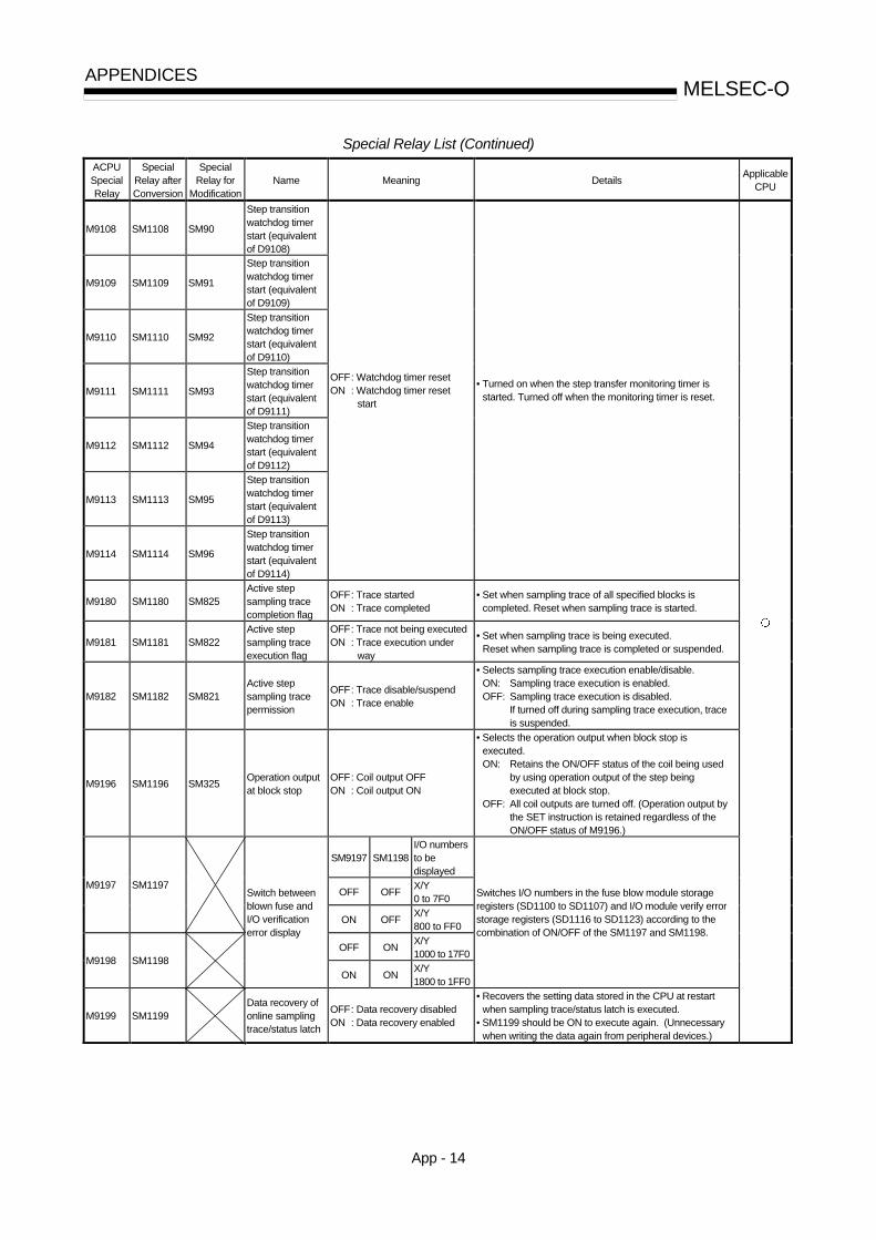
App - 14
MELSEC-Q APPENDICES
Special Relay List (Continued)
ACPU Special Relay
Special Relay after Conversion
Special Relay for
Modification Name Meaning Details Applicable
CPU
M9108 SM1108 SM90
Step transition watchdog timer start (equivalent of D9108)
M9109 SM1109 SM91
Step transition watchdog timer start (equivalent of D9109)
M9110 SM1110 SM92
Step transition watchdog timer start (equivalent of D9110)
M9111 SM1111 SM93
Step transition watchdog timer start (equivalent of D9111)
M9112 SM1112 SM94
Step transition watchdog timer start (equivalent of D9112)
M9113 SM1113 SM95
Step transition watchdog timer start (equivalent of D9113)
M9114 SM1114 SM96
Step transition watchdog timer start (equivalent of D9114)
OFF : Watchdog timer reset ON : Watchdog timer reset
start
• Turned on when the step transfer monitoring timer is started. Turned off when the monitoring timer is reset.
M9180 SM1180 SM825 Active step sampling trace completion flag
OFF : Trace started ON : Trace completed
• Set when sampling trace of all specified blocks is completed. Reset when sampling trace is started.
M9181 SM1181 SM822 Active step sampling trace execution flag
OFF : Trace not being executed ON : Trace execution under
way
• Set when sampling trace is being executed. Reset when sampling trace is completed or suspended.
M9182 SM1182 SM821 Active step sampling trace permission
OFF : Trace disable/suspend ON : Trace enable
• Selects sampling trace execution enable/disable. ON: Sampling trace execution is enabled. OFF: Sampling trace execution is disabled. If turned off during sampling trace execution, trace is suspended.
M9196 SM1196 SM325 Operation output at block stop
OFF : Coil output OFF ON : Coil output ON
• Selects the operation output when block stop is executed. ON: Retains the ON/OFF status of the coil being used by using operation output of the step being executed at block stop. OFF: All coil outputs are turned off. (Operation output by the SET instruction is retained regardless of the ON/OFF status of M9196.)
SM9197 SM1198 I/O numbers to be displayed
OFF OFF X/Y 0 to 7F0
M9197 SM1197
ON OFF X/Y 800 to FF0
OFF ON X/Y 1000 to 17F0
M9198 SM1198
Switch between blown fuse and I/O verification error display
ON ON X/Y 1800 to 1FF0
Switches I/O numbers in the fuse blow module storage registers (SD1100 to SD1107) and I/O module verify error storage registers (SD1116 to SD1123) according to the combination of ON/OFF of the SM1197 and SM1198.
M9199 SM1199 Data recovery of online sampling trace/status latch
OFF : Data recovery disabled ON : Data recovery enabled
• Recovers the setting data stored in the CPU at restart when sampling trace/status latch is executed.
• SM1199 should be ON to execute again. (Unnecessary when writing the data again from peripheral devices.)
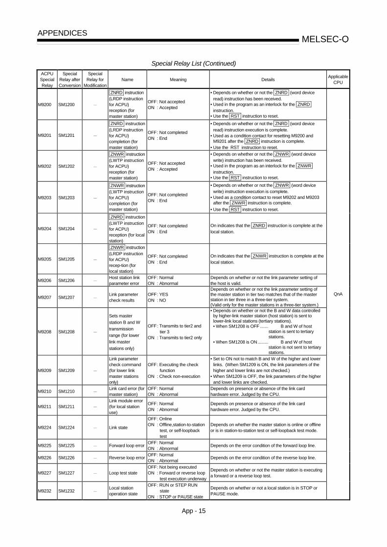
App - 15
MELSEC-Q APPENDICES
Special Relay List (Continued)
ACPU Special Relay
Special Relay after Conversion
Special Relay for
Modification Name Meaning Details Applicable
CPU
M9200 SM1200
ZNRD instruction (LRDP instruction for ACPU) reception (for master station)
OFF : Not accepted ON : Accepted
• Depends on whether or not the ZNRD (word device read) instruction has been received.
• Used in the program as an interlock for the ZNRD instruction.
• Use the RST instruction to reset.
M9201 SM1201
ZNRD instruction (LRDP instruction for ACPU) completion (for master station)
OFF : Not completed ON : End
• Depends on whether or not the ZNRD (word device read) instruction execution is complete.
• Used as a condition contact for resetting M9200 and M9201 after the ZNRD instruction is complete.
• Use the RST instruction to reset.
M9202 SM1202
ZNWR instruction (LWTP instruction for ACPU) reception (for master station)
OFF : Not accepted ON : Accepted
• Depends on whether or not the ZNWR (word device write) instruction has been received.
• Used in the program as an interlock for the ZNWR instruction.
• Use the RST instruction to reset.
M9203 SM1203
ZNWR instruction (LWTP instruction for ACPU) completion (for master station)
OFF : Not completed ON : End
• Depends on whether or not the ZNWR (word device write) instruction execution is complete.
• Used as a condition contact to reset M9202 and M9203 after the ZNWR instruction is complete.
• Use the RST instruction to reset.
M9204 SM1204
ZNRD instruction (LWTP instruction for ACPU) reception (for local station)
OFF : Not completed ON : End
On indicates that the ZNRD instruction is complete at the local station.
M9205 SM1205
ZNWR instruction (LRDP instruction for ACPU) recep-tion (for local station)
OFF : Not completed ON : End
On indicates that the ZNWR instruction is complete at the local station.
M9206 SM1206 Host station link parameter error
OFF : Normal ON : Abnormal
Depends on whether or not the link parameter setting of the host is valid.
M9207 SM1207 Link parameter check results
OFF : YES ON : NO
Depends on whether or not the link parameter setting of the master station in tier two matches that of the master station in tier three in a three-tier system. (Valid only for the master stations in a three-tier system.)
M9208 SM1208
Sets master
station B and W
transmission
range (for lower
link master
stations only)
OFF : Transmits to tier2 and tier 3
ON : Transmits to tier2 only
• Depends on whether or not the B and W data controlled by higher-link master station (host station) is sent to lower-link local stations (tertiary stations). • When SM1208 is OFF ....... B and W of host
station is sent to tertiary stations.
• When SM1208 is ON......... B and W of host station is not sent to tertiary stations.
M9209 SM1209
Link parameter check command (for lower link master stations only)
OFF : Executing the check function
ON : Check non-execution
• Set to ON not to match B and W of the higher and lower links. (When SM1209 is ON, the link parameters of the higher and lower links are not checked.)
• When SM1209 is OFF, the link parameters of the higher and lower links are checked.
M9210 SM1210 Link card error (for master station)
OFF : Normal ON : Abnormal
Depends on presence or absence of the link card hardware error. Judged by the CPU.
M9211 SM1211
Link module error (for local station use)
OFF : Normal ON : Abnormal
Depends on presence or absence of the link card hardware error. Judged by the CPU.
M9224 SM1224 Link state
OFF : Online ON : Offline,station-to-station
test, or self-loopback test
Depends on whether the master station is online or offline or is in station-to-station test or self-loopback test mode.
M9225 SM1225 Forward loop error OFF : Normal ON : Abnormal
Depends on the error condition of the forward loop line.
M9226 SM1226 Reverse loop error OFF : Normal ON : Abnormal
Depends on the error condition of the reverse loop line.
M9227 SM1227 Loop test state OFF : Not being executed ON : Forward or reverse loop
test execution underway
Depends on whether or not the master station is executing a forward or a reverse loop test.
M9232 SM1232 Local station operation state
OFF : RUN or STEP RUN state
ON : STOP or PAUSE state
Depends on whether or not a local station is in STOP or PAUSE mode.
QnA

App - 16
MELSEC-Q APPENDICES
Special Relay List (Continued)
ACPU Special Relay
Special Relay after Conversion
Special Relay for
Modification Name Meaning Details Applicable
CPU
M9233 SM1233 Local station error detect state
OFF : No errors ON : Error detection
Depends on whether or not a local station has detected an error in another station.
M9235 SM1235
Local station,remote I/O station parameter error detect state
OFF : No errors ON : Error detection
Depends on whether or not a local or a remote I/O station has detected any link parameter error in the master station
M9236 SM1236
Local station,remote I/O station initial communications state
OFF : No communications ON : Communications
underway
Depends on whether or not a local or a remote I/O station is communicating initial data (such as parameters) with the master station.
M9237 SM1237
Local station,remote I/O station error
OFF : Normal ON : Abnormal
Depends on the error condition of a local or remote I/O station.
M9238 SM1238
Local station,remote I/O station forward or reverse loop error
OFF : Normal ON : Abnormal
Depends on the error condition of the forward and reverse loop lines of a local or a remote I/O station.
M9240 SM1240 Link state
OFF : Online ON : Offline,station-to-
stationtest, or self-loopback test
Depends on whether the local station is online or offline, or is in station-to-station test or self-loopback test mode.
M9241 SM1241 Forward loop line error
OFF : Normal ON : Abnormal
Depends on the error condition of the forward loop line.
M9242 SM1242 Reverse loop line error
OFF : Normal ON : Abnormal
Depends on the error condition of the reverse loop line.
M9243 SM1243 Loopback implementation
OFF : Loopback not being conducted
ON : Loopback implementation
Depends on whether or not loopback is occurring at the local station.
M9246 SM1246 Data not received OFF : Reception ON : No reception
Depends on whether or not data has been received from the master station.
M9247 SM1247 Data not received OFF : Reception ON : No reception
Depends on whether or not a tier three station has received data from its master station in a three-tier system.
M9250 SM1250 Parameters not received
OFF : Reception ON : No reception
Depends on whether or not link parameters have been received from the master station.
M9251 SM1251 Link relay OFF : Normal ON : Abnormal
Depands on the data link condition at the local station.
M9252 SM1252 Loop test state OFF : Not being executed ON : Forward or reverse loop
test execution underway
Depends on whether or not the local station is executing a forward or a reverse loop test.
M9253 SM1253 Master station operation state
OFF : RUN or STEP RUN state ON : STOP or PAUSE state
Depends on whether or not the master station is in STOP or PAUSE mode.
M9254 SM1254
Local station other than host station operation state
OFF : RUN or STEP RUN state ON : STOP or PAUSE state
Depends on whether or not a local station other than the host is in STOP or PAUSE mode.
M9255 SM1255
Local station other than host station error
OFF : Normal ON : Abnormal
Depends on whether or not a local station other than the host is in error.
QnA

App - 17
MELSEC-Q APPENDICES
Special Relay List
(10) For redundant systems (Host system CPU information 1) for Q4AR only SM1510 to SM1599 are only valid for redundant systems. All off for standalone systems.
Number Name Meaning Explanation Set by (When Set)
ACPU M9
Applicable CPU
SM1500 Hold mode OFF : No-hold ON : Hold
• Specifies whether or not to hold the output value when a range over occurs for the S.IN instruction range check.
U New
SM1501 Hold mode OFF : No-hold ON : Hold
• Specifies whether or not the output value is held when a range over occurs for the S.OUT instruction range check.
U New
SM1510 Operation mode
OFF : Redundant system backup mode, independent system
ON : Redundant system separate mode
• Turns on when the operating mode is redundant system separate.
S (Each END)
New
SM1511 Start mode when power supply is on
OFF: System A fixed mode
ON : Previous control system latch mode
• Turns on when the start mode for a redundant system when the power is turned on is the previous control system latch mode.
S (Initial) New
SM1512 Start mode when CPU is started
OFF : Initial start ON : Hot start
• Turns on when the CPU operation mode is hot start when the redundant system is started up.
S (Initial) New
SM1513 Operation status when CPU is started
OFF : Initial start ON : Hot start
• Turns on when the CPU operation mode is hot start when the redundant system is actually start up.
S (Initial) New
SM1514 Operation mode when CPU is switched
OFF : Initial start ON : Hot start
• Turns on when the operation is hot start when the CPU operation is switched for a redundant system.
S (Initial) New
SM1515 Output hold mode OFF : Output reset ON : Output hold
• Turns on when the output mode during a stop error is output hold.
S (Each END)
New
SM1516 Operation system status
OFF : Control system ON : Standby system
• Turns on when the CPU operation system status is the standby system.
S (Status change)
New
SM1517 CPU startup status
OFF : Power supply on startup
ON : Operation system switch starup
• Turns on when the CPU is started up by the operation system switch.
• Reset using the user program.
S (Status change) /U
New
SM1518 Tracking execution mode
OFF : Batch operation mode
ON : Carryover mode
• When turned off when the tracking memory is in use during END, standby is executed until execution is possible.
• When turned on when the tracking memory is being used-during END, this is repeatedly executed until the next END
U New
SM1520 SM1520 Block 1
SM1521 SM1521 Block 2
SM1522 SM1522 Block 3
SM1523 SM1523 Block 4
SM1524 SM1524 Block 5
SM1525 SM1525 Block 6
SM1526 SM1526 Block 7
SM1527 SM1527 Block 8
SM1528 SM1528 Block 9
SM1529 SM1529 Block 10
SM1530 SM1530 Block 11
SM1531 SM1531 Block 12
SM1532 SM1532 Block 13
SM1533 SM1533 Block 14
SM1534 SM1534 Block 15
SM1535 SM1535 Block 16
SM1536 SM1536 Block 17
SM1537 SM1537 Block 18
SM1538 SM1538 Block 19
SM1539 SM1539 Block 20
SM1540 SM1540 Block 21
SM1541 SM1541 Block 22
SM1542 SM1542 Block 23
SM1543 SM1543 Block 24
SM1544 SM1544 Block 25
SM1545
Data tracking transmission link specification
OFF : No trigger ON : Trigger
SM1545 Block 26
• Specified the blocks to trigger when the data is transmitted by the data tracking instruction S. TRUCK.
U New
Q4AR

App - 18
MELSEC-Q APPENDICES
Special Relay List (Continued)
Number Name Meaning Explanation Set by (When Set)
ACPU M9
Applicable CPU
SM1546 SM1546 Block 27 SM1547 SM1547 Block 28
SM1548 SM1548 Block 29
SM1549 SM1549 Block 30
SM1550 SM1550 Block 31
SM1551 SM1551 Block 32
SM1552 SM1552 Block 33
SM1553 SM1553 Block 34
SM1554 SM1554 Block 35
SM1555 SM1555 Block 36
SM1556 SM1556 Block 37
SM1557 SM1557 Block 38
SM1558 SM1558 Block 39
SM1559 SM1559 Block 40
SM1560 SM1560 Block 41
SM1561 SM1561 Block 42
SM1562 SM1562 Block 43
SM1563 SM1563 Block 44
SM1564 SM1564 Block 45
SM1565 SM1565 Block 46
SM1566 SM1566 Block 47
SM1567 SM1567 Block 48
SM1568 SM1568 Block 49
SM1569 SM1569 Block 50
SM1570 SM1570 Block 51
SM1571 SM1571 Block 52
SM1572 SM1572 Block 53
SM1573 SM1573 Block 54
SM1574 SM1574 Block 55
SM1575 SM1575 Block 56
SM1576 SM1576 Block 57
SM1577 SM1577 Block 58
SM1578 SM1578 Block 59
SM1579 SM1579 Block 60
SM1580 SM1580 Block 61
SM1581 SM1581 Block 62
SM1582 SM1582 Block 63
SM1583
Data tracking transmission link specification
OFF : No trigger ON : Trigger
SM1583 Block 64
• Specified the blocks to trigger when the data is transmitted by the data tracking instruction S. TRUCK.
U
SM1590 Switching status from the network module
OFF : Normal ON : Switching
unsuccessful
• Turns on when could not be executed normally when the network module detects a network error and issues a switching request to the host system CPU.
S (Error ocurrs)
New Q4AR

App - 19
MELSEC-Q APPENDICES
Special Relay List
(11) For redundant system (Other system CPU information 1) for Q4AR only SM1600 to SM1650 only valid for the CPU redundant system backup mode, so they cannot be refreshed during the separate mode.Either the backup mode or the separate mode is valid for the SM4651 to SM1699. SM1600 to SM1699 are all turned off for standalone system.
Number Name Meaning Explanation Set by
(When Set) ACPU
M9 2
Applicable CPU
SM1600 Diagnosis error OFF : No error ON : Error
• Turns on if a error occurs in the diagnosis results. (Including external diagnosis)
• Remains on even if returns to normal thereafter.
S (Each END)
SM0
SM1601 Self diagnosis error
OFF : No self diagnosis error
ON : Self diagnosis error
• Turns on when an error occurs in the self-diagnosis results.
• Remains on even if returns to normal thereafter.
S (Each END)
SM1
SM1605 Error common information
OFF : No error common information
ON : Error common information
• Turns on when there is error common information and the SM1600 is on.
S (Each END)
SM5
SM1616 Error individual information
OFF : No error individual information
ON : Error individual information
• Turns on when there is error individual information and the SM1600 is on.
S (Each END)
SM16
SM1653 STOP contact STOP status • Turns on when in the STOP status. S
(Each END) SM203
SM1654 PAUSE contact PAUSE status • Turns on when in the PAUSE status. S
(Each END) SM204
SM1655 STEP-RUN contact STEP-RUN status • Turns on when in the STEP-RUN status. S
(Each END) SM205
Q4AR
1 Stores other system CPU diagnostic information and system information.
2 This shows the special relay(SM ) for the host system CPU. (12) For redundant system (tracking) for Q4AR only
Either the backup mode or the second mode is valid for SM1700 to SM1799. All is turned off for standalone system.
Number Name Meaning Explanation Set by (When Set)
ACPU M9
Applicable CPU
SM1700 Tracking execution flag
OFF : Execution not possible
ON : Execution possible
• Turns on when tracking is executed normally. S (status change)
New
SM1712 SM1712 Block 1
SM1713 SM1713 Block 2
SM1714 SM1714 Block 3
SM1715 SM1715 Block 4
SM1716 SM1716 Block 5
SM1717 SM1717 Block 6
SM1718 SM1718 Block 7
SM1719 SM1719 Block 8
SM1720 SM1720 Block 9
SM1721 SM1721 Block 10
SM1722 SM1722 Block 11
SM1723 SM1723 Block 12
SM1724 SM1724 Block 13
SM1725 SM1725 Block 14
SM1726 SM1726 Block 15
SM1727 SM1727 Block 16
SM1728 SM1728 Block 17
SM1729 SM1729 Block 18
SM1730 SM1730 Block 19
SM1731 SM1731 Block 20
SM1732 SM1732 Block 21
SM1733
Transmission trigger end flag
OFF : Transmission uncompleted
ON : Transmission end
SM1733 Block 22
• One scan turns on when the corresponding data transmission has been completed.
S (status change)
New
Q4AR

App - 20
MELSEC-Q APPENDICES
Special Relay List (Continued)
Number Name Meaning Explanation Set by (When Set)
ACPU M9
Applicable CPU
SM1734 SM1734 Block 23 SM1735 SM1735 Block 24
SM1736 SM1736 Block 25
SM1737 SM1737 Block 26
SM1738 SM1738 Block 27
SM1739 SM1739 Block 28
SM1740 SM1740 Block 29
SM1741 SM1741 Block 30
SM1742 SM1742 Block 31
SM1743 SM1743 Block 32
SM1744 SM1744 Block 33
SM1745 SM1745 Block 34
SM1746 SM1746 Block 35
SM1747 SM1747 Block 36
SM1748 SM1748 Block 37
SM1749 SM1749 Block 38
SM1750 SM1750 Block 39
SM1751 SM1751 Block 40
SM1752 SM1752 Block 41
SM1753 SM1753 Block 42
SM1754 SM1754 Block 43
SM1755 SM1755 Block 44
SM1756 SM1756 Block 45
SM1757 SM1757 Block 46
SM1758 SM1758 Block 47
SM1759 SM1759 Block 48
SM1760 SM1760 Block 49
SM1761 SM1761 Block 50
SM1762 SM1762 Block 51
SM1763 SM1763 Block 52
SM1764 SM1764 Block 53
SM1765 SM1765 Block 54
SM1766 SM1766 Block 55
SM1767 SM1767 Block 56
SM1768 SM1768 Block 57
SM1769 SM1769 Block 58
SM1770 SM1770 Block 59
SM1771 SM1771 Block 60
SM1772 SM1772 Block 61
SM1773 SM1773 Block 62
SM1774 SM1774 Block 63
SM1775
Transmission trigger end flag
OFF : Transmission uncompleted
ON : Transmission end
SM1775 Block 64
• One scan turns on when the corresponding data transmission has been completed.
S (status change)
New Q4AR

App - 21
MELSEC-Q APPENDICES
APPENDIX 2 Special Register List
The special registers, SD, are internal registers with fixed applications in the
programmable controller.
For this reason, it is not possible to use these registers in sequence programs in the
same way that normal registers are used.
However, it is possible to write data to them in order to conduct Q/QnACPU controls.
Data stored in the special registers are stored as BIN values if no special designation
has been made to the contrary.
The headings in the table that follows have the following meanings.
Item Function of Item
Number • Indicates special register number
Name • Indicates name of special register
Meaning • Indicates contents of special register
Explanation • Discusses contents of special register in more detail
Set by (When set)
• Indicates whether the relay is set by the system or user, and, if it is set by the system, when
setting is performed.
<Set by>
S : Set by system
U : Set by user (sequence programs or test operations from peripheral devices)
S/U : Set by both system and user
<When set> Indicated only for registers set by system
Each END : Set during each END processing
Initial : Set only during initial processing (when power supply is turned ON,
or when going from STOP to RUN)
Status change : Set only when there is a change in status
Error : Set when error occurs
Instruction execution : Set when instruction is executed
Request : Set only when there is a user request (through SM, etc.)
Corresponding ACPU
M9
• Indicates corresponding special register in ACPU (D9 )(Change and notation when
there has been a change in contents)
• Items indicated as "New" have been newly added for QnACPU
Corresponding CPU
• Indicates the corresponding CPU type name.
: Can be applied to all types of CPU
QCPU: Can be applied to Q-series CPU
QnA: Can be applied to QnA series and Q2ASCPU series
Each CPU type name: Can be applied only to the specific CPU. (e.g. Q4ARCPU, Q3ACPU)
For details on the following items, see these manuals:
• Networks • MELSECNET/10H Network System Reference Manual for Q
• MELSECNET/10 Network System Reference Manual for QnA
• SFC QCPU (Q mode)/QnACPU Programming Manual (SFC)
POINT
(1) SD1200 to SD1255 are used for QnACPU.
These relays are vacant with QCPU.
(2) Special register SD1500 and later are dedicated for Q4ARCPU.
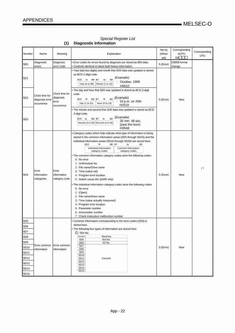
App - 22
MELSEC-Q APPENDICES
Special Register List
(1) Diagnostic Information
Number Name Meaning Explanation
Set by
(When
set)
Corresponding
ACPU
D9
Corresponding
CPU
SD0 Diagnostic
errors
Diagnosis
error code
• Error codes for errors found by diagnosis are stored as BIN data.
• Contents identical to latest fault history information. S (Error)
D9008 format
change
SD1
• Year (last two digits) and month that SD0 data was updated is stored
as BCD 2-digit code.
Year (0 to 99) Month (1 to 12)
B15 B7 B0B8to to(Example) : October, 1995 H9510
SD2
• The day and hour that SD0 was updated is stored as BCD 2-digit
code.
Day (1 to 31) Hour (0 to 23)
B15 B7 B0B8to to (Example) : 10 p.m. on 25th H2510
SD3
Clock time for
diagnosis error
occurrence
Clock time for
diagnosis
error
occurrence
• The minute and second that SD0 data was updated is stored as BCD
2-digit code.
Minutes (0 to 59)
B15 B7 B0B8to to(Example) : 35 min. 48 sec. (past the hour) H3548
Seconds (0 to 59)
S (Error) New
SD4
Error
information
categories
Error
information
category code
• Category codes which help indicate what type of information is being
stored in the common information areas (SD5 through SD15) and the
individual information areas (SD16 through SD26) are stored here.
Individual informationcategory codes
Common informationcategory codes
B15 B7 B0B8to to
• The common information category codes store the following codes:
0 : No error
1 : Unit/module No.
2 : File name/Drive name
3 : Time (value set)
4 : Program error location
5 : Switch cause (for Q4AR only) • The individual information category codes store the following codes:
0 : No error
1 : (Open)
2 : File name/Drive name
3 : Time (value actually measured)
4 : Program error location
5 : Parameter number
6 : Annunciator number
7 : Check instruction malfunction number
S (Error) New
SD5
SD6
SD7
SD8
SD9
SD10
SD11
SD12
SD13
SD14
SD15
Error common
information
Error common
information
• Common information corresponding to the error codes (SD0) is
stored here.
• The following four types of information are stored here:
1 Slot No.
SD5SD6SD7SD8SD9
SD10SD11SD12SD13SD14SD15
MeaningSlot No.I/O No.
(Vacant)
Number
S (Error) New

App - 23
MELSEC-Q APPENDICES
Special Register List (Continued)
Number Name Meaning Explanation
Set by
(When
set)
Corresponding
ACPU
D9
Corresponding
CPU
SD5
SD6
SD7
SD8
SD9
SD10
SD11
SD12
SD13
SD14
(Continued)
2 File name/Drive name
Number
SD5SD6SD7SD8SD9SD10SD11SD12SD13SD14SD15
Meaning
Drive
2EH(.)
File name
(ASCII code: 8 characters)
(Vacant)
42H(B) 41H(A)44H(D) 43H(C)46H(F) 45H(E)48H(H) 47H(G)49H(I) 2DH(.)4BH(K) 4AH(B)
B15 to B8 B7 to B0
(Example)File name=ABCDEFGH. IJK
Extension
(ASCII code: 3 characters)
3 Time (value set)
Number
SD5SD6SD7SD8SD9
SD10SD11SD12SD13SD14SD15
MeaningTime : 1 µs units (0 to 999 µs)
(Vacant)
Time : 1 ms units (0 to 65535 ms)
4 Program error location
Number
SD5SD6SD7SD8SD9
SD10SD11SD12SD13SD14SD15
Meaning
2EH(.)
File name
(ASCII code: 8 characters)
Extension(ASCII code: 3 characters)
PatternBlock No.
Step No./transition No.Sequence step No. (L)Sequence step No. (H)
Contents of pattern data
SFC block designation present (1)/absent (0)
000 0 to
0123415 14 to
SFC step designation present (1)/absent (0)SFC transition designation present (1)/absent (0)
(Not used)
(Bit number)
S (Error) New
SD15
Error
common
information
Error common
information
5 Switch cause
Switch direction (0:standby system to control system/ 1: control system to standby system)
Number
SD5
SD6
SD7SD8SD9SD10SD11SD12SD13SD14SD15
MeaningSwitch cause (0: automatic switch/ 1: manual switch)
(Vacant)
Tracking flag
Tracking flag contents
Shows whether or not the tracking data is valid.
Invalid work data invalid (0) /valid (1)
000 0 to0123415 14 to
System data (SFC active step information) invalid (0)/ valid (1)Switching cause invalid (0)/ valid (1)
(Not used)
(Bit number)
S (Error) New Q4AR
: Refer to REMARK in APP-25.

App - 24
MELSEC-Q APPENDICES
Special Register List (Continued)
Number Name Meaning Explanation
Set by
(When
set)
Corresponding
ACPU
D9
Corresponding
CPU
SD16
SD17
SD18
SD19
SD20
SD21
SD22
SD23
SD24
SD25
• Individual information corresponding to error codes (SD0) is stored
here.
1 File name/Drive name
Number
SD16SD17SD18SD19SD20SD21SD22SD23SD24SD25SD26
Meaning
Drive
2EH(.)
File name
(ASCII code: 8 characters)
(Vacant)
42H(B) 41H(A)44H(D) 43H(C)46H(F) 45H(E)48H(H) 47H(G)49H(I) 2DH(.)4BH(K) 4AH(B)
B15 to B8 B7 to B0
(Example)File name=ABCDEFGH. IJK
Extension
(ASCII code: 3 characters)
2 Time (value actu1ally measured)
Number
SD16SD17SD18SD19SD20SD21SD22SD23SD24SD25SD26
MeaningTime : 1 µs units (0 to 999 µs)
(Vacant)
Time : 1 ms units (0 to 65535 ms)
3 Program error location
Number
SD16SD17SD18SD19SD20SD21SD22SD23SD24SD25SD26
Meaning
2EH(.)
File name
(ASCII code: 8 characters)
Extension(ASCII code: 3 characters)
PatternBlock No.
Step No./transition No.
Sequence step No. (L)Sequence step No. (H)
Contents of pattern data
SFC block designation present (1)/absent (0)
000 0 to
0123415 14 to
SFC step designation present (1)/absent (0)SFC transition designation present (1)/absent (0)
(Not used)
(Bit number)
4 Parameter number 5 Annunciator
number / CHK
instruction
malfunction
number
6 Intelligent function
module parameter
error
(for QCPU only)
SD26
Error individual
information
Error
individual
information
Number
SD16SD17SD18SD19SD20SD21SD22SD23SD24SD25SD26
MeaningNo.
(Vacant)
Number
SD16SD17SD18SD19SD20SD21SD22SD23SD24SD25SD26
MeaningParameter No.
(Vacant)1
Number
SD16SD17
SD18SD19SD20SD21SD22SD23SD24SD25
SD26
Meaning
(Vacant)
Parameter No.
Error code for intelligent
function module
S (Error) New
: Refer to REMARK in APP-25.
1: For details of parameters, refer to User's Manual of the CPU you are using.

App - 25
MELSEC-Q APPENDICES
Special Register List (Continued)
Number Name Meaning Explanation Set by
(When set)
Corresponding
ACPU
D9
Corresponding
CPU
SD50 Error reset Error number that
performs error reset • Stores error number that performs error reset U New
SD51 Battery low
latch
Bit pattern
indicating where
battery voltage drop
occurred
• All corresponding bits go ON when battery voltage drops.
• Subsequently, these remain ON even after battery voltage has
been returned to normal. B4 B3 B0B2 B1
CPU error
Memory card A alarm
Memory card A error
Memory card B alarm
Memory card B error
0< >-------------------
• When QCPU is used, this flag is always OFF because memory
card B is used as standard memory.
S (Error) New
SD52 Battery low
Bit pattern
indicating where
battery voltage drop
occurred
• Same configuration as SD51 above
• Subsequently, goes OFF when battery voltage is restored to
normal.
• When QCPU is used, this flag is always OFF because memory
card B is used as standard memory.
S (Error) New
SD53 AC DOWN
detection
Number of times for
AC DOWN
• 1 is added to the stored value each time the input voltage
becomes 85 % or less of the rating while the CPU module is
operating, and the value is stored in BIN code.
S (Error) D9005
SD54 MINI link
errors
Error detection
state
1 The relevant station bit goes ON when any of the Installed
MINI (-S3) X(n+0)/X(n+20), X(n+6)/(n+26), X(n+7)/(n+27) or
X(n+8)/X(n+28) goes ON.
2 Goes ON when communications between the installed MINI
(-S3) and the CPU are not possible. B15 B8B9 B0
8th
module
8th
module
1st
module
1st
module.........
Information on Information on 12
S (Error) D9004 format
change QnA
SD60 Blown fuse
number
Number of module
with blown fuse
• Value stored here is the lowest station I/O number of the module
with the blown fuse. S (Error) D9000
SD61
I/O module
verification
error number
I/O module
verification error
module number
• The lowest I/O number of the module where the I/O module
verification number took place. S (Error) D9002
SD62 Annunciator
number
Annunciator
number • The first annunciator number to be detected is stored here.
S
(Instruction
execution)
D9009
SD63 Number of
annunciators
Number of
annunciators • Stores the number of annunciators searched.
S
(Instruction
execution)
D9124
REMARK
1) Extensions are shown below. SD10 SD11
Higher8 bits Lower8 bits Higher8 bits Extension name File type
51H 50H 41H QPA Parameters 51H 50H 47H QPG Sequence program/SFC program 51H 43H 44H QCD Device comment 51H 44H 49H QDI Device initial value 51H 44H 52H QDR File register 51H 44H 53H QDS Simulation data 51H 44H 4CH QDL Local device 51H 54H 53H QTS Sampling trace data (For QnA) 51H 54H 4CH QTL Status latch data (For QnA) 51H 54H 50H QTP Program trace data (For QnA) 51H 54H 52H QTR SFC trace file 51H 46H 44H QFD Trouble history data

App - 26
MELSEC-Q APPENDICES
Special Register List (Continued)
Number Name Meaning Explanation Set by
(When set)
Corresponding
ACPU
D9
Corresponding
CPU
SD64 D9125
SD65 D9126
SD66 D9127
SD67 D9128
SD68 D9129
SD69 D9130
SD70 D9131
SD71 D9132
SD72 New
SD73 New
SD74 New
SD75 New
SD76 New
SD77 New
SD78 New
SD79
Table of
detected
annunciator
numbers
Annunciator
detection
number
When F goes ON due to OUT F or SET F , the F numbers which
go progressively ON from SD64 through SD79 are registered. F numbers turned OFF by RST F are deleted from SD64 to SD79,
and are shifted to the data register following the data register where
the deleted F numbers had been stored. Execution of the LED R instruction shifts the contents of SD64 to
SD79 up by one.
(This can also be done by using the INDICATOR RESET switch on
the front of the CPU of the Q3A/Q4ACPU.)
After 16 annunciators have been detected, detection of the 17th will
not be stored from SD64 through SD79.
SD62 0 50 50 50 50 50 50 50 50 50 50 50 99 ...(Number detected)
SD63 0 1 2 3 2 3 4 5 6 7 8 9 8
0 50 50 50 50 50 50 50 50 50 50 50 99SD64
SD65
SD66
SD67
SD68
SD69
SD70
SD71
SD72
SD73
SD74
SD75
SD76
SD77
SD78
SD79
0 0 25 25 99 99 99 99 99 99 99 99 15
0 0 0 99 0 15 15 15 15 15 15 15 70
0 0 0 0 0 0 70 70 70 70 70 70 65
0 0 0 0 0 0 0 65 65 65 65 65 38
0 0 0 0 0 0 0 0 38 38 38 38 110
0 0 0 0 0 0 0 0 0 110 110 110 151
0 0 151
0
0 0 0 0 0 0 0 0 151 210
00 0 0 0 0 0 0 0 0 0210
0 00 0 0 0 0 0 0 0 0 00
0 00 0 0 0 0 0 0 0 0 00
0 00 0 0 0 0 0 0 0 0 00
0 00 0 0 0 0 0 0 0 0 00
0 00 0 0 0 0 0 0 0 0 00
0 00 0 0 0 0 0 0 0 0 00
0 00 0 0 0 0 0 0 0 0 00
...(Number of annunciators detected)
(Number
detected)
SET
F50
SET
F25
SET
F99
RET
F25
SET
F15
SET
F70
SET
F65
SET
F38
SET
F110
SET
F151
SET
F210LEDR
S
(Instruction
execution)
New
SD80 CHK number CHK number • Error codes detected by the CHK instruction are stored as BCD
code.
S
(Instruction
execution)
New
SD90 Corresponds to SM90 D9108
SD91 Corresponds to SM91 D9109
SD92 Corresponds to SM92 D9110
SD93 Corresponds to SM93 D9111
SD94 Corresponds to SM94 D9112
SD95 Corresponds to SM95 D9113
SD96 Corresponds to SM96 D9114
SD97 Corresponds to SM97 New
SD98 Corresponds to SM98 New
SD99
Step transition
watchdog
timer setting
value
(Enabled only
when SFC
program
exists)
F number for
timer set value
and time over
error
Corresponds to SM99
• F numbers which go ON at step transition
watchdog timer set value and watchdog timer
over errors. B15 B7 B0B8
F number setting (0 to 255)
Timer time limit setting (1 to 255 sec: (1-second units))
• Timer is started by turning SM90 through
SM99 ON during active step, and if the
transition conditions for the relevant steps are
not met within the timer limits, the designated
annunciator (F) will go ON.
U
New
SD105
CH1
transmission
speed setting
(RS232)
Stores the
preset
transmission
speed when
GPP function
is used.
K3 : 300bps, K6 : 600bps, K24 : 2400bps, K48 : 4800bps
K96 : 9600bps, K192 : 19.2kbps, K384 : 38.4kbps
K576 : 57.6kbps, K1152 : 115.2kbps
S New QCPU

App - 27
MELSEC-Q APPENDICES
Special Register List
(2) System information
Number Name Meaning Explanation Set by
(When set)
Corresponding
ACPU
D9
Corresponding
CPU
SD120
Error No. for
external
power supply
OFF
Module No.
which has
external
power supply
error
• Stores the smallest head No. of the module whose external power
supply is OFF.
Applicable only for Q-series modules (For future use)
S (Error) New
• The CPU switch status is stored in the following format: BF BCBB B8 B7 B4 B3 B0
Vacant3 2 1 1 : CPU switch status 0: RUN
1: STOP
2: L.CLR 2 : Memory card switch Always OFF
3 : DIP switch B8 through BC correspond to SW1
through SW5 of system setting
switch 1.
0: OFF, 1: ON
BD through BF are vacant.
S(Every
END
processing)
New
QCPU
• The CPU switch state is stored in the following format: B15 B12B11 B8 B7 B4 B3 B0
Vacant3 2 1
1 : CPU key
State of switch 0 : RUN
1 : STOP
2 : L.CLR
2 : Memory cards switch B4 corresponds to card A, and B5
corresponds to card B
OFF at 0; ON at 1
3 : DIP switch B8 through B12 correspond to
SW1 through SW5 of system
setting switch 1.
B14 and B15 correspond to SW1
and SW2 of system setting switch
2, respectively.
OFF at 0; ON at 1
SD200 State of
switch
State of CPU
switch
S(Every
END
processing)
New QnA
• The following bit patterns are used to store the statuses of the LEDs
on the CPU: BF BCBB B8 B7 B4 B3 B0
8 3 2 14567
1 : RUN
2 : ERROR
3 : USER
4 : BAT.ALARM
5 : BOOT
6 : Vacant
7 : Vacant
8 : MODE
Bit patterns for MODE
0: OFF, 1: Green, 2:
Orange
S (Status
change) New QCPU
• Information concerning which of the following states the LEDs on the
CPU are in is stored in the following bit patterns:
• 0 is off, 1 is on, and 2 is flicker B15 B12B11 B8 B7 B4 B3 B0
8 3 2 14567
1 : RUN
2 : ERROR
3 : USER
4 : BAT.ALARM
5 : BOOT
6 : CARD A (Memory card)
7 : CARD B (Memory card)
8 : Vacant
SD201 LED status State of CPU-
LED
S (Status
change) New QnA

App - 28
MELSEC-Q APPENDICES
Special Register List (Continued)
Number Name Meaning Explanation Set by
(When set)
Corresponding
ACPU
D9
Corresponding
CPU
SD202 LED off
Bit pattern of
LED that is
turned off
• Stores bit patterns of LEDs turned off
(Only USER and BOOT enabled)
• Turned off at 1, not turned off at 0
U New QnA
• The CPU operating state is stored as indicated in the following
figure: B15 B12B11 B8 B7 B4 B3 B0
2 1 1 : Operating state of CPU 0 :RUN
1 :STEP-RUN
2 :STOP
3 :PAUSE
2 : STOP/PAUSE cause 0 :Key switch
1 :Remote contact
2 :Peripheral, computer link,or
operation from some other
remote source
3 :Internal program instruction
Note: Priority is earliest first 4 :Errors
SD203 Operating
state of CPU
Operating
state of CPU
S (Every
END
processing)
D9015 format
change
SD207 Priorities 1 to
4 D9038
SD208 Priorities 5 to
8
D3039 format
change
SD209
LED display
priority
ranking Priorities 9 to
10
• When error is generated, the LED display (flicker) is made according
to the error number setting priorities.
• The setting areas for priorities are as follows: B15 B12B11 B8 B7 B4 B3 B0
Priority 4 Priority 3 Priority 2 Priority 1SD207Priority 8 Priority 7 Priority 6 Priority 5SD208
Priority 10 Priority 9SD209 Default Value SD207=H4321
SD208=H8765
SD207=H00A9
• No display is made if "0" is set.
However, even if "0" has been set, information concerning CPU
operation stop (including parameter settings) errors will be indicated
by the LEDs without conditions.
See Section 7.9.5 REMARK for the priority order.
U
New
SD210 Clock data Clock data
(year, month)
• The year (last two digits) and month are stored as BCD code at
SD210 as shown below: B15 B12.......... B11 B8........... B7 B4............ B3 B0.............
Year Month
Example :July 1993H9307
D9025
SD211 Clock data Clock data
(day, hour)
• The day and hour are stored as BCD code at SD211 as shown
below: B15 B12.......... B11 B8........... B7 B4............ B3 B0.............
Day Hour
Example :31st, 10 a.m.H3110
D9026
SD212 Clock data
Clock data
(minute,
second)
• The minutes and seconds (after the hour) are stored as BCD code at
SD212 as shown below: Example :B15 B12.......... B11 B8........... B7 B4............ B3 B0.............
Minute Second
35 min., 48 sec.(after the hour)H3548
S/U
(Request)
D9027

App - 29
MELSEC-Q APPENDICES
Special Register List (Continued)
Number Name Meaning Explanation Set by
(When set)
Corresponding
ACPU
D9
Corresponding
CPU
• The day of the week is stored as BCD code at SD213 as shown
below: B15 B12.......... B11 B8........... B7 B4............ B3 B0.............
Higher digits of year (0 to 99)
Day of week
0
1
2
3
4
5
6
Sunday
Monday
Tuesday
Wednesday
Thursday
Friday
Saturday
Example :Friday H0005
S/U
(Request) D9028 QCPU
SD213 Clock data Clock data
(day of week) • The day of the week is stored as BCD code at SD213 as shown
below: B15 B12.......... B11 B8........... B7 B4............ B3 B0.............
Always set "0"
Day of week
0
1
2
3
4
5
6
Sunday
Monday
Tuesday
Wednesday
Thursday
Friday
Saturday
Example :Friday H0005
S/U
(Request) D9028 QnA
SD220
SD221
SD222
SD223
SD224
SD225
SD226
SD227
LED display
data
Display indicator
data
• LED display ASCII data (16 characters) stored here.
SD220
SD221
SD222
SD223
SD224
SD225
SD226
SD226
15th character from the right
13th character from the right
11th character from the right
9th character from the right
7th character from the right
5th character from the right
3rd character from the right
1st character from the right
16th character from the right
14th character from the right
12th character from the right
10th character from the right
8th character from the right
6th character from the right
4th character from the right
2nd character from the right
toB15 B8 toB7 B0
S (When
changed) New
SD240 Base mode 0: Automatic mode
1: Detail mode • Stores the base mode. S (Initial) New
SD241
No. of
expansion
bases
0: Basic only
1 to 7: No. of
expansion
bases
• Stores the maximum number of the expansion bases being
installed. S (Initial) New
SD242 A/Q base
differentiation
Base type
differentiation
0: QA B is
installed
(A mode)
1: Q B is
installed
(Q mode)
0
Fixed to 0
Basic base
127
1st expansion base
to
2nd expansion base
7th expansion base
to
bit No.
When no expansion
base is installed, the
value is fixed to 0.
S (Initial) New
SD243
SD244
No. of base
slots No. of base slots
SM243 Expansion 3 Expansion 2 Expansion 1 Basic
Expansion 7 Expansion 6 Expansion 5 Expansion 4SM244
F C B 8 7 4 3 0 bit No.
• As shown above, each area stores the number of slots being
installed.
S (Initial) New
QCPU
SD250 Loaded
maximum I/O
Loaded maximum
I/O No.
• When SM250 goes from OFF to ON, the upper 2 digits of the
final I/O number plus 1 of the modules loaded are stored as BIN
values.
S (Request
END) New
SD251
Head I/O
number for
replacement
Head I/O No. for
module
replacement
• Stores the upper two digits of the first I/O number of an I/O
module that is removed/replaced in the online status.(default
value : 100H)
U D9094
Q2A (S1)
Q3A
Q4A
Q4AR
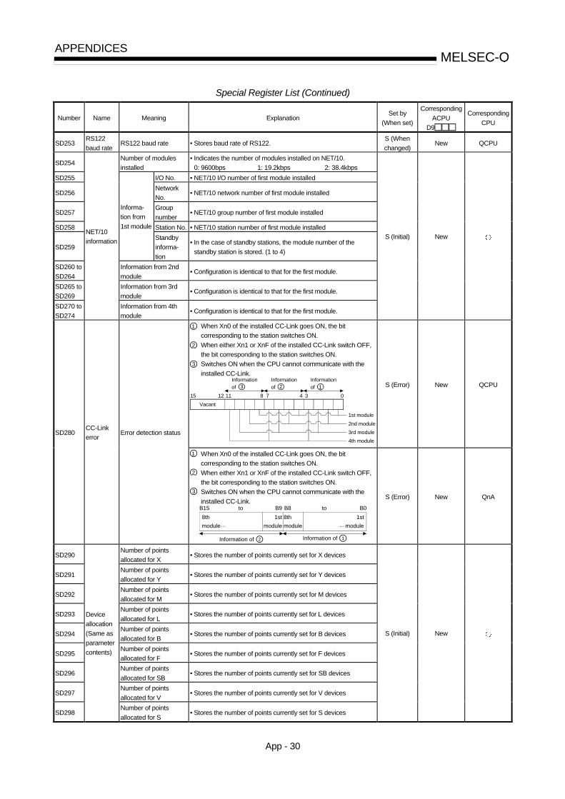
App - 30
MELSEC-Q APPENDICES
Special Register List (Continued)
Number Name Meaning Explanation Set by
(When set)
Corresponding
ACPU
D9
Corresponding
CPU
SD253 RS122
baud rate RS122 baud rate • Stores baud rate of RS122.
S (When
changed) New QCPU
SD254 Number of modules
installed
• Indicates the number of modules installed on NET/10.
0: 9600bps 1: 19.2kbps 2: 38.4kbps
SD255 I/O No. • NET/10 I/O number of first module installed
SD256 Network
No. • NET/10 network number of first module installed
SD257 Group
number • NET/10 group number of first module installed
SD258 Station No. • NET/10 station number of first module installed
SD259
Informa-
tion from
1st module
Standby
informa-
tion
• In the case of standby stations, the module number of the
standby station is stored. (1 to 4)
SD260 to
SD264
Information from 2nd
module • Configuration is identical to that for the first module.
SD265 to
SD269
Information from 3rd
module • Configuration is identical to that for the first module.
SD270 to
SD274
NET/10
information
Information from 4th
module • Configuration is identical to that for the first module.
S (Initial) New
1 When Xn0 of the installed CC-Link goes ON, the bit
corresponding to the station switches ON.
2 When either Xn1 or XnF of the installed CC-Link switch OFF,
the bit corresponding to the station switches ON.
3 Switches ON when the CPU cannot communicate with the
installed CC-Link.
0
1st module
2nd module
3rd module
3478111215
Vacant
4th module
Information
of 1Information
of 2Information
of 3
S (Error) New QCPU
SD280 CC-Link
error Error detection status
1 When Xn0 of the installed CC-Link goes ON, the bit
corresponding to the station switches ON. 2 When either Xn1 or XnF of the installed CC-Link switch OFF,
the bit corresponding to the station switches ON. 3 Switches ON when the CPU cannot communicate with the
installed CC-Link. B15 B8B9 B0
8th
module
8th
module
1st
module
1st
module...
toto
...
Information of 1Information of 2
S (Error) New QnA
SD290 Number of points
allocated for X • Stores the number of points currently set for X devices
SD291 Number of points
allocated for Y • Stores the number of points currently set for Y devices
SD292 Number of points
allocated for M • Stores the number of points currently set for M devices
SD293 Number of points
allocated for L • Stores the number of points currently set for L devices
SD294 Number of points
allocated for B • Stores the number of points currently set for B devices
SD295 Number of points
allocated for F • Stores the number of points currently set for F devices
SD296 Number of points
allocated for SB • Stores the number of points currently set for SB devices
SD297 Number of points
allocated for V • Stores the number of points currently set for V devices
SD298
Device
allocation
(Same as
parameter
contents)
Number of points
allocated for S • Stores the number of points currently set for S devices
S (Initial) New
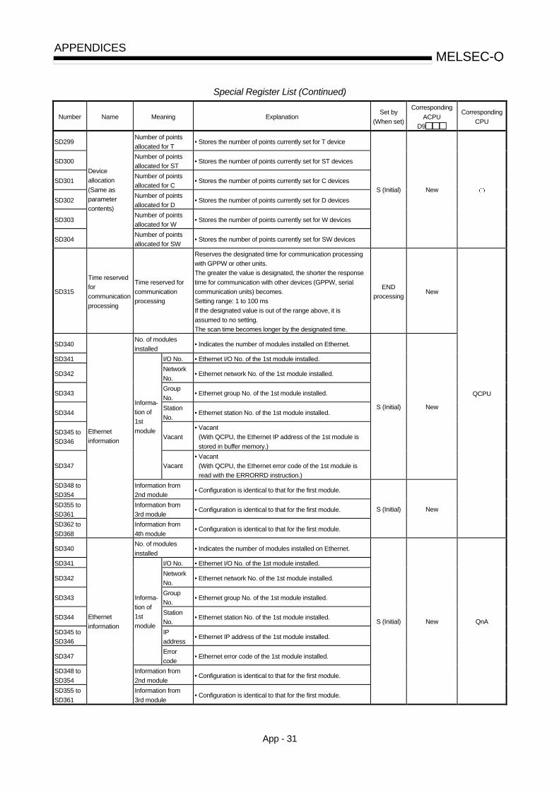
App - 31
MELSEC-Q APPENDICES
Special Register List (Continued)
Number Name Meaning Explanation Set by
(When set)
Corresponding
ACPU
D9
Corresponding
CPU
SD299 Number of points
allocated for T • Stores the number of points currently set for T device
SD300 Number of points
allocated for ST • Stores the number of points currently set for ST devices
SD301 Number of points
allocated for C • Stores the number of points currently set for C devices
SD302 Number of points
allocated for D • Stores the number of points currently set for D devices
SD303 Number of points
allocated for W • Stores the number of points currently set for W devices
SD304
Device
allocation
(Same as
parameter
contents)
Number of points
allocated for SW • Stores the number of points currently set for SW devices
S (Initial) New
SD315
Time reserved
for
communication
processing
Time reserved for
communication
processing
Reserves the designated time for communication processing
with GPPW or other units.
The greater the value is designated, the shorter the response
time for communication with other devices (GPPW, serial
communication units) becomes.
Setting range: 1 to 100 ms
If the designated value is out of the range above, it is
assumed to no setting.
The scan time becomes longer by the designated time.
END
processing New
SD340 No. of modules
installed • Indicates the number of modules installed on Ethernet.
SD341 I/O No. • Ethernet I/O No. of the 1st module installed.
SD342 Network
No. • Ethernet network No. of the 1st module installed.
SD343 Group
No. • Ethernet group No. of the 1st module installed.
SD344 Station
No. • Ethernet station No. of the 1st module installed.
SD345 to
SD346 Vacant
• Vacant
(With QCPU, the Ethernet IP address of the 1st module is
stored in buffer memory.)
SD347
Informa-
tion of
1st
module
Vacant
• Vacant
(With QCPU, the Ethernet error code of the 1st module is
read with the ERRORRD instruction.)
S (Initial) New
SD348 to
SD354
Information from
2nd module • Configuration is identical to that for the first module.
SD355 to
SD361
Information from
3rd module • Configuration is identical to that for the first module.
SD362 to
SD368
Ethernet
information
Information from
4th module • Configuration is identical to that for the first module.
S (Initial) New
QCPU
SD340 No. of modules
installed • Indicates the number of modules installed on Ethernet.
SD341 I/O No. • Ethernet I/O No. of the 1st module installed.
SD342 Network
No. • Ethernet network No. of the 1st module installed.
SD343 Group
No. • Ethernet group No. of the 1st module installed.
SD344 Station
No. • Ethernet station No. of the 1st module installed.
SD345 to
SD346
IP
address • Ethernet IP address of the 1st module installed.
SD347
Informa-
tion of
1st
module
Error
code • Ethernet error code of the 1st module installed.
SD348 to
SD354
Information from
2nd module • Configuration is identical to that for the first module.
SD355 to
SD361
Ethernet
information
Information from
3rd module • Configuration is identical to that for the first module.
S (Initial) New QnA

App - 32
MELSEC-Q APPENDICES
Special Register List (Continued)
Number Name Meaning Explanation Set by
(When set)
Corresponding
ACPU
D9
Corresponding
CPU
SD362 to
SD368
Ethernet
information
Information from
4th module • Configuration is identical to that for the first module. S (Initial) New
SD380
Instruction
reception status
of 1st module
B0
Instruction reception status of channel 1Instruction reception status of channel 2
B1B2B3B4B5B6B7B8B15
Instruction reception status of channel 3Instruction reception status of channel 4Instruction reception status of channel 5Instruction reception status of channel 6Instruction reception status of channel 7Instruction reception status of channel 8
ON: Received (Channel is used.)OFF: Not received (Channel is not used.)
00 to
Not used
SD381 Information from
2nd module • Configuration is identical to that for the first module.
SD382 Information from
3rd module • Configuration is identical to that for the first module.
SD383
Ethernet
instruction
reception
status
Information from
4th module • Configuration is identical to that for the first module.
S (Initial) New
SD392 Software
version
Internal system
software version
• Stores the internal system software version in ASCII code.
Higher byte Lower byte
The data in the lower byte position is indefinite.The software version is stored in the higher byte position.
For version "A", for example, "41H" is stored. Note: The internal system software version may differ from the
version indicated by the version symbol printed on the
case.
S (Initial) D9060
QnA
(3) System clocks/counters
Number Name Meaning Explanation Set by
(When set)
Corresponding
ACPU
D9
Corresponding
CPU
SD412 1 second
counter
Number of counts in
1-second units
• Following programmable controller CPU RUN, 1 is added each
second
• Count repeats from 0 to 32767 to -32768 to 0
S (Status
change) D9022
SD414
2n second
clock
setting
2n second clock
units
• Stores value n of 2n second clock (Default is 30)
• Setting can be made between 1 and 32767 U New
SD415 2nms clock
setting 2nms clock units
• Stores value n of 2nms clock (Default is 30)
• Setting can be made between 1 and 32767 U New QCPU
SD420 Scan
counter
Number of counts in
each scan
• Incremented by 1 for each scan execution after the PC CPU is
set to RUN.
• Count repeats from 0 to 32767 to -32768 to 0
S(Every
END
processing)
New
SD430
Low speed
scan
counter
Number of counts in
each scan
• Incremented by 1 for each scan execution after the PC CPU is
set to RUN.
• Count repeats from 0 to 32767 to -32768 to 0
• Used only for low speed execution type programs
S(Every
END
processing)
New
: Not counted by the scan in an initial execution type program.

App - 33
MELSEC-Q APPENDICES
Special Register List
(4) Scan information
Number Name Meaning Explanation Set by
(When set)
Corresponding
ACPU
D9
Corresponding
CPU
SD500 Execution
program No.
Execution type of
program being
executed
• Program number of program currently being executed is
stored as BIN value.
S (Status
change) New
SD510 Low speed
program No.
File name of low
speed execution in
progress
• Program number of low speed program currently being
executed is stored as BIN value.
• Enabled only when SM510 is ON.
S (Every
END
processing) New
SD520 Current scan time
(in 1 ms units)
• Stores current scan time (in 1 ms units)
Range from 0 to 65535
S (Every
END
processing)
D9017 format
change
SD521
Current scan
time Current scan time
(in 1 µs units)
• Stores current scan time (in 1 µs units)
Range from 00000 to 900
(Example)
A current scan of 23.6 ms would be stored as follows:
D520=23
D521=600
S (Every
END
processing) New
SD522 Initial scan time
(in 1 ms units)
• Stores scan time for first scan (in 1 ms units)
• Range from 0 to 65535
SD523
Initial scan
time Initial scan time
(in 100 µs units)
• Stores scan time for first scan (in 1 µs units)
• Range of 000 to 900
S (First
END
processing) New
SD524 Minimum scan time
(in 1 ms units)
• Stores minimum value of scan time (in 1 ms units)
• Range from 0 to 65535
S (Every
END
processing)
D9018 format
change
SD525
Minimum scan
time Minimum scan time
(in 100 µs units)
• Stores minimum value of scan time (in 100 µs units)
• Range of 000 to 900
S (Every
END
processing) New
SD526 Maximum scan time
(in 1 ms units)
• Stores maximum value of scan time, excepting the first
scan. (in 1 ms units) • Range from 0 to 65535
D9019 format
change
SD527
Maximum scan
time Maximum scan time
(in 100 µs units)
• Stores maximum value of scan time, excepting the first
scan. (in 100 µs units) • Range of 000 to 900
S (Every
END
processing) New
SD528 Current scan time
(in 1 ms units)
• Stores current scan time for low speed execution type
program (in 1 ms units)
SD529
For low speed
execution type
programs
current scan
time
Current scan time
(in 100 µs units)
• Stores current scan time for low speed execution type
program (in 100 µs units) • Range of 000 to 900
S (Every
END
processing) New
SD532 Minimum scan time
(in 1 ms units)
• Stores minimum value of scan time for low speed execution
type program (in 1 ms units) • Range from 0 to 65535
SD533
Minimum scan
time for low
speed
execution type
programs Minimum scan time
(in 100 µs units)
• Stores minimum value of scan time for low speed execution
type program (in 100 µs units) • Range of 000 to 900
S (Every
END
processing) New
SD534 Maximum scan time
(in 1 ms units)
• Stores the maximum scan time for all except low speed
execution type program's first scan. (in 1 ms units) • Range from 0 to 65535
SD535
Maximum scan
time for low
speed
execution type
programs Maximum scan time
(in 100 µs units)
• Stores the maximum scan time for all except low speed
execution type program's first scan. (in 100 µs units) • Range of 000 to 900
S (Every
END
processing) New
SD540 END processing time
(in 1 ms units)
• Stores time from completion of scan program to start of next
scan. (in 1 ms units) • Range from 0 to 65535
SD541
END
processing
time END processing time
(in 100 µs units)
• Stores time from completion of scan program to start of next
scan. (in 100 µs units) • Range of 000 to 900
S (Every
END
processing) New
SD542 Constant scan wait
time (in 1 ms units)
• Stores wait time when constant scan time has been set.
(in 1 ms units) • Range from 0 to 65535
SD543
Constant scan
wait time Constant scan wait
time (in 100 µs units)
• Stores wait time when constant scan time has been set.
(in 100 µs units) • Range of 000 to 900
S (First
END
processing) New

App - 34
MELSEC-Q APPENDICES
Special Register List (Continued)
Number Name Meaning Explanation Set by
(When set)
Corresponding
ACPU
D9
Corresponding
CPU
SD544
Cumulative
execution time for
low speed execution
type programs
(in 1 ms units)
• Stores cumulative execution time for low speed execution
type programs. (in 1 ms units) • Range from 0 to 65535 • Cleared to 0 following 1 low speed scan
SD545
Cumulative
execution time
for low speed
execution type
programs
Cumulative
execution time for
low speed execution
type programs
(in 100 µs units)
• Stores cumulative execution time for low speed execution
type programs. (in 100 µs units) • Range of 000 to 900 • Cleared to 0 following 1 low speed scan
S (Every
END
processing) New
SD546
Execution time for
low speed execution
type programs
(in 1 ms units)
• Stores low speed program execution time during 1 scan
(in 1 ms units)
• Range from 0 to 65535
• Stores each scan
SD547
Execution time
for low speed
execution type
programs Execution time for
low speed execution
type programs
(in 100 µs units)
• Stores low speed program execution time during 1 scan
(in 100 µs units)
• Range of 000 to 900
• Stores each scan
S (Every
END
processing) New
SD548
Scan program
execution time
(in 1 ms units)
• Stores execution time for scan execution type program
during 1 scan (in 1 ms units)
• Range from 0 to 65535
• Stores each scan
SD549
Scan program
execution time Scan program
execution time
(in 100 µs units)
• Stores execution time for scan execution type program
during 1 scan (in 100 µs units)
• vRange of 000 to 900
• Stores each scan
S (Every
END
processing) New
SD550
Service
interval
measurement
module
Unit/module No. • Sets I/O number for module that measures service interval U New
SD551
Module service
interval
(in 1 ms units)
• When SM551 is ON, stores service interval for module
designated by SD550. (in 1 ms units)
• Range from 0 to 65535
SD552
Service
interval time Module service
interval
(in 100 µs units)
• When SM551 is ON, stores service interval for module
designated by SD550. (in 1 µs units)
• Range from 000 to 999
S
(Request) New

App - 35
MELSEC-Q APPENDICES
Special Register List
(5) Memory card
Number Name Meaning Explanation Set by
(When set)
Corresponding
ACPU
D9
Corresponding
CPU
• Indicates memory card A model installed
Drive 1
(RAM) model
Drive 2
(ROM) model
0: Does not exist
1: SRAM
0: Does not exist
(1: SRAM)
2: ATA FRASH
3: FLASH ROM
B4 B3 B0B8 B7BF
0< >0-----------
S (Initial and card
removal) New QCPU
SD600
Memory
card A
models
Memory
card A
models • Indicates memory card A model installed B4 B3 B0
Drive 1
(RAM) model
Drive 2
(ROM) model
0< >0
0: Does not exist
1: SRAM
0: Does not exist
2: EEPROM
3: Flash ROM
B8 B7B15
-----------
S (Initial and card
removal) New QnA
S (Initial and card
removal) New QCPU
SD602
Drive 1
(RAM)
capacity
Drive 1
capacity • Drive 1 capacity is stored in 1 K byte units
S (Initial and card
removal) New QnA
S (Initial and card
removal) New QCPU
SD603
Drive 2
(ROM)
capacity
Drive 2
capacity • Drive 2 capacity is stored in 1 K byte units
S (Initial and card
removal) New QnA
• The use conditions for memory card A are stored as bit patterns
(In use when ON)
• The significance of these bit patterns is indicated below:
B0: Boot operation (QBT)
B1: Parameters (QPA)
B2: Device comments (QCD)
B3: Device initial value (QDI)
B4: File register R (QDR)
B5: Trace (QTS)
B6:
B7:
B8:
B9: CPU fault history (QFD)
BA: SFC trace (QTS)
BB: Local device (QDL)
BC:
BD:
BE:
BF:
S (Status change) New QCPU
• The use conditions for memory card A are stored as bit patterns
(In use when ON)
• The significance of these bit patterns is indicated below:
B0: Boot operation (QBT)
B1: Parameters (QPA)
B2: Device comments (QCD)
B3: Device initial value (QDI)
B4: File register R (QDR)
B5: Sampling trace (QTS)
B6: Status latch (QTL)
B7: Program trace (QTP)
B8: Simulation data (QDS)
B9: CPU fault history (QFD)
B10: SFC trace (QTS)
B11: Local device (QDL)
B12:
B13:
B14:
B15:
SD604
Memory
card A use
conditions
Memory
card A
use
conditions
S (Status change) New QnA
SD620
Memory
card B
models
Memory
card B
models
• Indicates memory card B models installed
Drive 3
(RAM) model
Drive 4
(ROM) model
(0: Does not exist)
1: SRAM
0: Does not exist
(1: SRAM)
(2: E PROM)
3: FLASH ROM
B4 B3 B0B8 B7BF
0< >0-----------
2
Drive 4 is fixed to "3" because it has built-in flash ROM.
S (Initial) New QCPU

App - 36
MELSEC-Q APPENDICES
Special Register List (Continued)
Number Name Meaning Explanation
Set by
(When
set)
Corresponding
ACPU
D9
Corresponding
CPU
SD620 Memory card
B models
Memory card
B models
• Indicates memory card B models installed B4 B3 B0
Drive 1
(RAM) model
Drive 2
(ROM) model
0< >0
0: Does not exist
1: SRAM
0: Does not exist
2: EEPROM
3: Flash ROM
B8 B7B15
-----------
S (Initial) New
Q2A (S1)
Q3A
Q4A
Q4AR
• Drive 3 capacity is stored in 1 K byte units.
(Fixed to "61" because it has 61 KB RAM built-in.) S (Initial) New QCPU
SD622
Drive 3
(RAM)
capacity
Drive 3
capacity • Drive 3 capacity is stored in 1 K byte units S (Initial) New
Q2A (S1)
Q3A
Q4A
Q4AR
• Drive 4 capacity is stored in 1 K byte units. S (Initial) New QCPU
SD623
Drive 4
(ROM)
capacity
Drive 4
capacity • Drive 4 capacity is stored in 1 K byte units S (Initial) New
Q2A (S1)
Q3A
Q4A
Q4AR
• The conditions for usage for drive 3/4 are stored as bit patterns.
(In use when ON)
• The significance of these bit patterns is indicated below:
B0: Boot operation (QBT)
B1: Parameters (QPA)
B2: Device comments (QCD)
B3: Device initial value (QDI)
B4: File R (QDR)
B5: Trace (QTS)
B6:
B7:
B8:
B9: CPU fault history (QFD)
B10: SFC trace (QTS)
B11: Local device (QDL)
B12:
B13:
B14:
B15:
Drive 3/4 use
conditions
Drive 3/4 use
conditions
S (Status
change) New QCPU
• The use conditions for memory card B are stored as bit patterns
(In use when ON)
• The significance of these bit patterns is indicated below:
B0: Boot operation (QBT)
B1: Parameters (QPA)
B2: Device comments (QCD)
B3: Device initial value (QDI)
B4: File R (QDR)
B5: Sampling trace (QTS)
B6: Status latch (QCL)
B7: Program trace (QDL)
B8: Simulation data (QDS)
B9: CPU fault history (QFD)
B10: SFC trace (QTS)
B11: Local device (QDL)
B12:
B13:
B14:
B15:
SD624
Memory card
B use
conditions
Memory card
B use
conditions
S (Status
change) New
Q2A (S1)
Q3A
Q4A
Q4AR
SD640 File register
drive Drive number: • Stores drive number being used by file register S (Initial) New
SD641
SD642
SD643
SD644
SD645
SD646
File register
file name
File register
file name
• Stores file register file name (with extension) selected at parameters
or by use of QDRSET instruction as ASCII code.
SD641
SD642
SD643
SD644
SD645
SD646
Second character
Fourth character
Sixth character
Eighth character
First character of extension
Third character of extension
First character
Third character
Fifth character
Seventh character
2EH(.)
Second character of extension
B15 to B8 B7 to B0
S (Initial) New
SD647 File register
capacity
File register
capacity
• Stores the data capacity of the currently selected file register in 1 K
word units.
S (Status
change) New
SD648 File register
block number
File register
block number • Stores the currently selected file register block number.
S (Status
change) D9035
SD650 Comment
drive
Comment
drive number
• Stores the comment drive number selected at the parameters or by
the QCDSET instruction.
S (Status
change) New
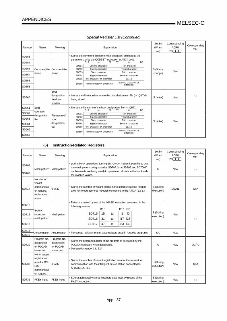
App - 37
MELSEC-Q APPENDICES
Special Register List (Continued)
Number Name Meaning Explanation
Set by
(When
set)
Corresponding
ACPU
D9
Corresponding
CPU
SD651
SD652
SD653
SD654
SD655
SD656
Comment file
name
Comment file
name
• Stores the comment file name (with extension) selected at the
parameters or by the QCDSET instruction in ASCII code.
SD651
SD652
SD653
SD654
SD655
SD656
Second character
Fourth character
Sixth character
Eighth character
First character of extension
Third character of extension
First character
Third character
Fifth character
Seventh character
2EH(.)
Second character of extension
B15 to B8 B7 to B0
S (Status
change) New
SD660
Boot
designation
file drive
number
• Stores the drive number where the boot designation file ( .QBT) is
being stored. S (Initial) New
SD661
SD662
SD663
SD664
SD665
SD666
Boot
operation
designation
file
File name of
boot
designation
file
• Stores the file name of the boot designation file ( .QBT).
SD661
SD662
SD663
SD664
SD665
SD666
Second character
Fourth character
Sixth character
Eighth character
First character of extension
Third character of extension
First character
Third character
Fifth character
Seventh character
2EH(.)
Second character of extension
B15 to B8 B7 to B0
S (Initial) New
(6) Instruction-Related Registers
Number Name Meaning Explanation
Set by
(When
set)
Corresponding
ACPU
D9
Corresponding
CPU
SD705
SD706
Mask pattern Mask pattern
• During block operations, turning SM705 ON makes it possible to use
the mask pattern being stored at SD705 (or at SD705 and SD706 if
double words are being used) to operate on all data in the block with
the masked values.
U New
SD714
Number of
vacant
communicati
on request
registration
areas
0 to 32 • Stores the number of vacant blocks in the communications request
area for remote terminal modules connected to the AJ71PT32-S3.
S (During
execution) M9081 QnA
SD715
SD716
SD717
IMASK
instruction
mask pattern
Mask pattern
• Patterns masked by use of the IMASK instruction are stored in the
following manner:
SD715
SD716
SD717
l15 l1 l0
l31
l47
l17
l33
l16
l32
B15 B0B11
to
to
to
S (During
execution) New
SD718
SD719 Accumulator Accumulator • For use as replacement for accumulators used in A-series programs. S/U New
SD720
Program No.
designation
for PLOAD
instruction
Program No.
designation
for PLOAD
instruction
• Stores the program number of the program to be loaded by the
PLOAD instruction when designated.
• Designation range: 1 to 124
U New QCPU
SD730
No. of vacant
registration
area for CC-
Link
communicati
on request
0 to 32
• Stores the number of vacant registration area for the request for
communication with the intelligent device station connected to
A(1S)J61QBT61.
S (During
execution) New QnA
SD736 PKEY input PKEY input • SD that temporarily stores keyboard data input by means of the
PKEY instruction.
S (During
execution) New

App - 38
MELSEC-Q APPENDICES
Special Register List (Continued)
Number Name Meaning Explanation
Set by
(When
set)
Corresponding
ACPU
D9
Corresponding
CPU
SD738
SD739
SD740
SD741
SD742
SD743
SD744
SD745
SD746
SD747
SD748
SD749
SD750
SD751
SD752
SD753
SD754
SD755
SD756
SD757
SD758
SD759
SD760
SD761
SD762
SD763
SD764
SD765
SD766
SD767
SD768
SD769
Message
storage
Message
storage
• Stores the message designated by the MSG instruction.
SD738SD739SD740SD741SD742SD743
1st characterB15 B8 B7 B0
SD744SD745SD746SD747SD748SD749SD750SD751SD752SD753SD754SD755SD756SD757SD758SD759SD760SD761SD762SD763SD764SD765SD766SD767SD768SD769 64th character
2nd character3rd character4th character5th character6th character7th character8th character9th character10th character
11th character12th character13th character14th character15th character16th character17th character18th character19th character20th character21st character22nd character23rd character24th character25th character26th character27th character28th character29th character30th character31st character32nd character33rd character34th character35th character36th character37th character38th character39th character40th character41st character42nd character43rd character44th character45th character46th character47th character48th character49th character50th character51st character52nd character53rd character54th character55th character56th character57th character58th character59th character60th character61st character62nd character63rd character
to to
S (During
execution) New
SD774
TO
SD775
PID limit
setting
0: Limit set
1: Limit not set
• Designate the limit for each PID loop as follows:
SD774
SD775
b15 b1 b0
Loop16
Loop32
Loop2
Loop18
Loop1
Loop17
to
to
U New QCPU
SD780
Remaining
No. of
simultaneous
execution of
CC-Link
dedicated
instruction
0 to 32 • Stores the remaining number of simultaneous execution of the CC-
Link dedicated instructions. U New QnA
SD781
TO
SD793
Mask pattern
of IMASK
instruction
Mask pattern
• Stores the mask patterns masked by the IMASK instruction as
follows:
SD781
SD782
SD793
l63 l59 l48
l79
l255
l65
l241
l64
l240
B15 B0B11
to
to
to
to
S (During
execution) New QCPU

App - 39
MELSEC-Q APPENDICES
Special Register List
(7) Debug
Number Name Meaning Explanation
Set by
(When
set)
Corresponding
ACPU
D9
Corresponding
CPU
SD806
SD807
SD808
SD809
SD810
SD811
Status latch
file name
Status latch
file name
• Stores file name (with extension) from point in time when status latch
was conducted as ASCII code.
SD806
SD807
SD808
SD809
SD810
SD811
First characterSecond character
Third characterFourth character
Fifth characterSixth character
seventh characterEighth character
B15 B8to B7 B0to
First character ofextension
2EH(.)
2nd character ofextension
Third character ofextension
S (During
execution) New
SD812 • Stores step number from point in time when status latch was
conducted.
SD813 SD812 Patterm
SD814 SD813 Block No.
SD815 SD814 Step No./transition No.
SD815 Sequence step No.(L)
SD816 Sequence step No.(H)
SD816
Status latch
step
Status latch
step Contents of pattern data
000 0
0123415 14
SFC transition designation present (1)/absent (0)
to
to
(Bit number)
(Not in use) SFC block designation present (1)/absent (0)
SFC block designation present (1)/absent (0)
S (During
execution)
D9055 format
change
QnA

App - 40
MELSEC-Q APPENDICES
Special Register List
(8) Latch area
Number Name Meaning Explanation
Set by
(When
set)
Corresponding
ACPU
D9
Corresponding
CPU
SD900
Drive where
power was
interrupted
Access file
drive number
during power
loss
• Stores drive number if file was being accessed during power loss. S (Status
change) New
SD901
SD902
SD903
SD904
SD905
SD906
File name
active during
power loss
Access file
name during
power loss
• Stores file name (with extension) in ASCII code if file was being
accessed during power loss.
SD901SD902SD903SD904
SD905
SD906
B15 B8 B7 B01st character2nd character3rd character4th character5th character6th character7th character8th character
to to
1st character ofextension 2EH(.)
2nd character ofextension
3rd character ofextension
S (Status
change) New
SD910
SD911
SD912
SD913
SD914
SD915
SD916
SD917
SD918
SD919
SD920
SD921
SD922
SD923
SD924
SD925
RKEY input RKEY input
• Stored in sequence that PU key code was entered.
SD910SD911SD912SD913SD914SD915
B15 B8 B7 B0
SD916SD917SD918SD919SD920SD921SD922SD923SD924SD925
1st character2nd character3rd character4th character5th character6th character7th character8th character9th character10th character11th character12th character13th character14th character15th character16th character17th character18th character19th character20th character21st character22nd character23rd character24th character25th character26th character27th character28th character29th character30th character31st character32nd character
to to
S (During
execution) New
QnA

App - 41
MELSEC-Q APPENDICES
(9) A to Q/QnA conversion correspondences
ACPU special registers D9000 to D9255 correspond to the special registers
SD1000 to SD1255 after A-series to the Q/QnA-series conversion.
These special registers are all set by the system, and users cannot use them to
set program data.
Users who need to set data with these registers should edit the special registers
for the Q/QnA.
However, before conversion users could set data at special registers D9200 to
D9255 only, and after conversion users can also set data at registers 1200 to
1255.
For more detailed information concerning the contents of the ACPU special
registers, see the individual CPU users manual, and the MELSECNET and
MELSECNET/B data link system reference manual.
REMARK
Supplemental explanation on "Special Register for Modification" column
1 For the device numbers for which a special register for modification is specified,
modify it to the special register for QCPU/QnACPU.
2 For the device numbers for which is specified, special register after
conversion can be used.
3 Device numbers for which is specified do not function for QCPU/QnACPU.
Special Register List ACPU
Special
Conversion
Special
Register after
Conversion
Special
Register for
Modification
Name Meaning Details Corresponding
CPU
D9000 SD1000 Fuse blown
Number of
module with
blown fuse
• When fuse blown modules are detected, the lowest
number of detected units is stored in hexadecimal.
(Example: When fuses of Y50 to 6F output modules have
blown, "50" is stored in hexadecimal) To monitor the
number by peripheral devices, perform monitor operation
given in hexadecimal.
(Cleared when all contents of SD1100 to SD1107 are reset
to 0.)
• Fuse blow check is executed also to the output modules of
remote I/O stations.
• Stores the module numbers corresponding to setting
switch numbers or base slot numbers when fuse blow
occurred.
I/O module for A0J2 Extension base unit
Setting
switch Stored data
Base unit
slot No. Stored data
0 1 0 5
1 2 1 6
2 3 2 7
3 4 3 8
4 5
5 6
6 7
7 8
D9001 SD1001 Fuse blown
Number of
module with
blown fuse

App - 42
MELSEC-Q APPENDICES
Special Register List (Continued)
ACPU
Special
Conversion
Special
Register after
Conversion
Special
Register for
Modification
Name Meaning Details Corresponding
CPU
D9002 SD1002 I/O module
verification error
I/O module
verification error
module number
• If I/O modules, of which data are different from data
entered, are detected when the power is turned on,
the first I/O number of the lowest number unit among
the detected units is stored in hexadecimal. (Storing
method is the same as that of SD1000.) To monitor
the number by peripheral devices, perform monitor
operation given in hexadecimal.
(Cleared when all contents of SD1116 to SD1123 are
reset to 0.)
• I/O module verify check is executed also to the
modules of remote I/O terminals.
D9004 SD1004 MINI link errors
Stores setting
status made at
parameters
(modules 1 to 8)
• Error status of the MINI(S3) link detected on loaded
AJ71PT32(S3) is stored. b15 b8 b7 b0
8 7 6 5 4 3 2 1 8 7 6 5 4 3 2 1
Bits which correspond to faulty
AJ71PT32(S3) are turned on.
Bits which correspond to the signals of
AJ71PT32(S3), shown below, are
turned on as the signals are turned on.
• Hardware error (X0/X20)
• MINI(S3) link error datection (X6/X26)
• MINI(S3) link communication error
(X7/X27)
QnA
D9005 SD1005 AC DOWN
counter
Number of times for
AC DOWN
• 1 is added each time input voltage becomes 85% or
less of rating while the CPU unit is performing
operation, and the value is stored in BIN code.
D9008 SD1008 SD0 Self-diagnostic
error
Self-diagnostic
error number
• When error is found as a result of self-diagnosis, error
number is stored in BIN code.
• When one of F0 to 255 is turned on by OUT F or
SET F , the F number, which has been detected
earliest among the F numbers which have turned on,
is stored in BIN code. • SD62 can be cleared by RST F or LEDR
instruction. If another F number has been detected,
the clearing of SD62 causes the next number to be
stored in SD62.
D9009 SD1009 SD62 Annunciator
detection
F number at which
external failure has
occurred
• When one of F0 to 255 is turned on by OUT F or
SET F , the F number, which has been detected
earliest among the F numbers which have turned on,
is stored in BIN code. • SD62 can be cleared by executing RST F or
LEDR instruction or moving INDICATOR RESET
switch on CPU front to ON position. If another F
number has been detected, the clearing of SD62
causes the nest number to be stored in SD62.
D9010 SD1010 Error step
Step number at
which operation
error has occurred.
• When operation error has occurred during execution
of application instruction, the step number, at which
the error has occurred, is stored in BIN code.
Thereafter, each time operation error occurs, the
contents of SD1010 are renewed.
D9011 SD1011 Error step
Step number at
which operation
error has occurred.
• When operation error has occurred during execution
of application instruction, the step number, at which
the error has occurred, is stored in BIN code. Since
storage into SD1011 is made when SM1011 changes
from off to on, the contents of SD1011 cannot be
renewed unless SM1011 is cleared by user program.
D9014 SD1014 I/O control mode I/O control mode
number
• The I/O control mode set is returned in any of the
following numbers:
0. Both input and output in direct mode
1. Input in refresh mode, output in direct mode
3. Both input and output in refresh mode

App - 43
MELSEC-Q APPENDICES
Special Register List (Continued)
ACPU
Special
Conversion
Special
Register after
Conversion
Special
Register for
Modification
Name Meaning Details Corresponding
CPU
D9015 SD1015 SD203 Operating state
of CPU
Operating state of
CPU
• The operation states of CPU as shown below are
stored in SD203.
CPU key switch
Remains the same in
remote RUN/STOP mode.
0 RUN
1 STOP
2
3 STEP RUN
Remote RUN/STOP
by parameter setting
PAUSE 1
Remote RUN/STOP
by computer
instruction
execution
STOP
Status in program
Except below
B15 B12 B11 B8 B7 B4 B3 B0
0 RUN
1 STOP
2 PAUSE 1
0 RUN
1 STOP
2 PAUSE 1
0
1
1 When the CPU is in RUN mode and SM1040 is off,
the CPU remains in RUN mode if changed to
PAUSE mode.
D9016 SD1016 Program
number
0: Main program
(ROM)
1: Main program
(RAM)
2: Subprogram 1
(RAM)
3: Subprogram 2
(RAM)
4: Subprogram 3
(RAM)
5: Subprogram 1
(ROM)
6: Subprogram 2
(ROM)
7: Subprogram 3
(ROM)
8: Main program
(E2PROM)
9: Subprogram 1
(E2PROM)
A: Subprogram 2
(E2PROM)
B: Subprogram 3
(E2PROM)
• Indicates which sequence program is run presently.
One value of 0 to B is stored in BIN code.
D9017 SD1017 SD520 Scan time Minimum scan time
(10 ms units)
• If scan time is smaller than the content of SD520, the
value is newly stored at each END. Namely, the
minimum value of scan time is stored into SD520 in
BIN code.
D9018 SD1018 SD524 Scan time Scan time
(10 ms units)
• Scan time is stored in BIN code at each END and
always rewritten.
D9019 SD1019 SD526 Scan time Maximum scan
time (10 ms units)
• If scan time is larger than the content of SD526, the
value is newly stored at each END. Namely, the
maximum value of scan time is stored into SD526 in
BIN code.
D9020 SD1020 Constant scan
Constant scan time
(User sets in 10 ms
units)
• Sets the interval between consecutive program starts
in multiples of 10 ms.
0: No setting
1 to 200: Set. Program is executed at intervals of
(set value) × 10 ms.
D9021 SD1021 Scan time Scan time
(1 ms units)
• Scan time is stored and updated in BIN code after
every END.

App - 44
MELSEC-Q APPENDICES
Special Register List (Continued)
ACPU
Special
Conversion
Special
Register after
Conversion
Special
Register for
Modification
Name Meaning Details Corresponding
CPU
D9022 SD1022 SD412 1 second
counter
Count in units of
1ms.
• When the PC CPU starts running, it starts counting 1
every second.
• It starts counting up from 0 to 32767, then down to
-32768 and then again up to 0. Counting repeats this
routine.
D9025 SD1025 SD210 Clock data Clock data
(year, month)
• Stores the year (2 lower digits) and month in BCD. B15 B12 B11 B8 B7 B4 B3 B0
Example: 1987, July H8707
Year Month
D9026 SD1026 SD211 Clock data Clock data
(day, hour)
• Stores the day and hour in BCD. B15 B12 B11 B8 B7 B4 B3 B0
Day Hour
Example
31th, 10 o'clock
H3110
D9027 SD1027 SD212 Clock data Clock data
(minute, second)
• Stores the Minute and second in BCD. B15 B12 B11 B8 B7 B4 B3 B0
Minute Second
Example:
35 minutes,
48 seconds
H3548
D9028 SD1028 SD213 Clock data Clock data
(day of week)
• Stores the day of the week in BCD. B15 B12 B11 B8 B7 B4 B3 B0 Example:
Friday
H0005
0 must be set. Day of the week
0
1
2
3
4
5
6
Sunday
Monday
Tuesday
Wednesday
Thursday
Friday
Saturday
D9035 SD1035 SD648 Extension file
register Use block No.
• Stores the block No. of the extension file register
being used in BCD code.
D9036 SD1036
D9037 SD1037
Extension file
registerfor
designation of
device number
Device number
when individual
devices from
extension file
register are directly
accessed
• Designate the device number for the extension file
register for direct read and write in 2 words at SD1036
and SD1037 in BIN data.
Use consecutive numbers beginning with R0 of block
No. 1 to designate device numbers.
SD1036,SD1037
0
1638316384
Block No.2 area
Device No. (BIN data)
Exetension file register
Block No.1 area
to
to
to
D9038 SD1038 SD207 Priorities 1 to 4
D9039 SD1039 SD208
LED display
priority ranking Priorities 5 to 7
• Sets priority of ERROR LEDs which illuminate (or
flicker) to indicate errors with error code numbers.
• Configuration of the priority setting areas is as shown
below.
SD207
SD208
b15 b12 b11 b8 b7 b4 b3 b0
Priority 4 Priority 3 Priority 2 Priority 1
Priority 5Priority 6Priority 7 • For details, refer to the applicable CPUs User’s
Manual and the ACPU (Fundamentals) Programming
manual.

App - 45
MELSEC-Q APPENDICES
Special Register List (Continued)
ACPU
Special
Conversion
Special
Register after
Conversion
Special
Register for
Modification
Name Meaning Details Corresponding
CPU
D9044 SD1044 For sampling
trace
Step or time during
sampling trace
• Turned on/off with a peripheral device.
At scanning --------- 0
At time---------------- Time (10 msec unit)
Stores the value in BIN code.
D9049 SD1049 Work area for
SFC
Block number of
extension file
register
• Stores the block number of the expansion file register
which is used as the work area for the execution of a
SFC program in a binary value.
• Stores "0" if an empty area of 16K bytes or smaller,
which cannot be expansion file register No. 1, is used
or if SM320 is OFF.
D9050 SD1050 SFC program
error number
Error code
generated by SFC
program
• Stores code numbers of errors occurred in the SFC
program in BIN code.
0: No error
80: SFC program parameter error
81: SFC code error
82: Number of steps of simultaneous execution
exceeded
83: Block start error
84: SFC program operation error
D9051 SD1051 Error block
Block number
where error
occurred
• Stores the block number in which an error occurred in
the SFC program in BIN code.
In the case of error 83 the starting block number is
stored.
D9052 SD1052 Step number where
error occurred
• Stores the step number in which error 84 occurred in
the SFC program in BIN code.
Stores "0" when errors 80, 81 and 82 occurred.
Stored the block starting step number when error 83
occurred.
D9053 SD1053 Error transition
Transition condition
number where error
occurred
• Stores the transfer condition number in which error 84
occurred in the SFC program in BIN code.
Stored "0" when errors 80, 81, 82 and 83 occurred.
D9054 SD1054 Error sequence
step
Sequence step
number where error
occurred
• Stores the sequence step number of transfer condition
and operation output in which error 84 occurred in the
SFC program in BIN code.
D9055 SD1055 SD812 Status latch Status latch step
• Stores the step number when status latch is executed.
• Stores the step number in a binary value if status latch
is executed in a main sequence program.
• Stores the block number and the step number if status
latch is executed in a SFC program.
Block No.(BIN)
Step No.(BIN)
Higher 8 bits Lower 8 bits
D9060 SD1060 SD392 Software version Software version of
internal software
(QnA)
• Stores the software version of the internal system in
ASCII code.
Higher byte Lower byte
The data in the lower byte position is indefinite.The software version is stored in the higher byte position.
For version "A", for example, "41H" is stored. Note: The software version of the initial system may
differ from the version indicated by the version
information printed on the rear of the case.
QnA
D9072 SD1072
PC
communications
check
Computer link data
check
• In the loopback test mode of individual AJ71C24
(S3/S6/S8), the AJ71C24 (S3/S6/S8) executes data
write/read and communication check.
D9081 SD1081 SD714
Number of
empty blocks in
communications
request
registrtion area
Number of empty
blocks in
communications
request registration
area
• Stores the number of communication requests
executed to remote terminal modules connected to
AJ71PT32 (S3), A2C and A52G.
• Subtracts 1 at completion of communication with a
remote terminal module.
QnA

App - 46
MELSEC-Q APPENDICES
Special Register List (Continued)
ACPU
Special
Conversion
Special
Register after
Conversion
Special
Register for
Modification
Name Meaning Details Corresponding
CPU
D9085 SD1085
Register for
setting time
check value
Default value 10s
• Sets the time check time of the data link instructions
(ZNRD, ZNWR) for the MELSECNET/10.
• Setting range: 1 s to 65535 s (1 to 65535)
• Setting unit: 1 s
• Default value: 10 s (If 0 has been set, default
10 s is applied)
D9090 SD1090
Number of
special functions
modules over
Number of special
functions modules
over
• For details, refer to the manual of each microcompu-
ter program package.
D9091 SD1091 Detailed error
code
Self-diagnosis
detailed error code • Stores the detail code of cause of an instruction error.
D9094 SD1094 SD251
Head I/O
number for
replacement
Head I/O number
for replacement
• Stores upper 2 digits of the head I/O address of I/O
modules to be loaded or unloaded during online mode
in BIN code. Example) Input module X2F0 → H2F
D9100 SD1100
D9101 SD1101
D9102 SD1102
D9103 SD1103
D9104 SD1104
D9105 SD1105
D9106 SD1106
D9107 SD1107
Fuse blown
module
Bit pattern in units
of 16 points,
indicating the
modules whose
fuses have blown
• Output module numbers (in units of 16 points), of
which fuses have blown, are entered in bit pattern.
(Preset output unit numbers when parameter setting
has been performed.) 15 14 13 12 11 10 9 8 7 6 5 4 3 2 1 0
000000001(Y80)
000000
0000000000000000
000000000000001Y7B0
SD1100
SD1101
SD1107
1(YCO)
Indicates fuse blow.
1Y730
• Fuse blow check is executed also to the output
module of remote I/O station.
(If normal status is restored, clear is not performed.
Therefore, it is required to perform clear by user
program.)
D9108 SD1108
D9109 SD1109
D9110 SD1110
D9111 SD1111
D9112 SD1112
D9113 SD1113
D9114 SD1114
Step transfer
monitoring timer
setting
Timer setting valve
and the f number at
time out
• Sets value for the step transfer monitoring timer and
the number of F which turns on when the monitoring
timer timed out.
Timer setting (1 to 255 sec in seconds)
F number setting
b15 b8 b7 b0to to
(By turning on any of MSM708 to SM1114, the
monitoring timer starts. If the transfer condition
following a step which corresponds to the timer is not
established within set time, set annunciator (F) is
tuned on.)
D9116 SD1116
D9117 SD1117
D9118 SD1118
D9119 SD1119
D9120 SD1120
D9121 SD1121
D9122 SD1122
D9123 SD1123
I/O module
verification error
Bit pattern, in units
of 16 points,
indicating the
modules with
verification errors.
• When I/O modules, of which data are different from
those entered at power-on, have been detected, the
I/O unit numbers (in units of 16 points) are entered in
bit pattern. (Preset I/O unit numbers when parameter
setting has been performed.) 15 14 13 12 11 10 9 8 7 6 5 4 3 2 1 0
0000000000000
000000000000000
000000000000001XY100
SD1116
SD1117
SD1123
1XY0
1XY100
0
0 0
Indicates I/O module verify error. • I/O module verify check is executed also to remote I/O
station modules.
(If normal status is restored, clear is not performed.
Therefore, it is required to perform clear by user
program.)

App - 47
MELSEC-Q APPENDICES
Special Register List (Continued)
ACPU
Special
Conversion
Special
Register after
Conversion
Special
Register for
Modification
Name Meaning Details Corresponding
CPU
D9124 SD1124 SD63
Annunciator
detection
quantity
Annunciator
detection quantity
• When one of F0 to 255 (F0 to 2047 for AuA and AnU) is turned on by SET F 1 is added to the contents of
SD63. When RST F or LEDR instruction is
executed, 1 is subtracted from the contents of SD63.
(If the INDICATOR RESET switch is provided to the
CPU, pressing the switch can execute the same
processing.) • Quantity, which has been turned on by SET F is
stored into SD63 in BIN code. The value of SD63 is
maximum 8.
D9125 SD1125 SD64
D9126 SD1126 SD65
D9127 SD1127 SD66
D9128 SD1128 SD67
D9129 SD1129 SD68
D9130 SD1130 SD69
D9131 SD1131 SD70
D9132 SD1132 SD71
Annunciator
detection
number
Annunciator
detection number
• When one of F0 to 255 (F0 to 2047 for AuA and AnU) is turned on by SET F , F number, which has turned
on, is entered into SD64 to SD71 in due order in BIN
code. • F number, which has been turned off by RST F , is
erased from SD64 to SD71, and the contents of data
registers succeeding the data register, where the
erased F number was stored, are shifted to the
preceding data registers. • By executing LEDR instruction, the contents of
SD64 to SD71 are shifted upward by one. (For A3N,
A3HCPU, it can be performed by use of INDICATOR
RESET switch on front of CPU module.)
• When there are 8 annunciator detections, the 9th one
is not stored into SD64 to SD71 even if detected.
0 50 50 50 50 50 50 50 50 50 50 50 99
0
0 50 50 50 50 50 50 50 50 50 50 99
0 25 25 99 99 99 99 99 99 99 99 15
1 2 3 2 3 4 5 6 7 8 8 8
50
0
0 99 15 15 15 15 15 15 15 700 0 0
0 70 70 70 70 70 70 650 0 00 0
0 65 65 65 65 65 380 0 00 0 0
0 38 38 38 38 1100 0 00 0 0 0
0 110 110 110 1510 0 00 0 0 0
0 151 151 2100 0 00 0 0 0
0
0 0
SD62
SD63
SD64
SD65
SD66
SD67
SD68
SD69
SD70
SD71
SETF50
SETF25
SETF99
RSTF25
SETF15
SETF70
SETF65
SETF38
SETF110
SETF151
SETF210 LEDR

App - 48
MELSEC-Q APPENDICES
Special Register List
(10) Special register list dedicated for QnA ACPU
Special
Conversion
Special
Register after
Conversion
Special
Register for
Modification
Name Meaning Details Corresponding
CPU
Stores the execution result of the ZNRD (word device
read) instruction
• ZNRD instruction setting
fault:
Faulty setting of the ZNRD instruction
constant, source,
and/or destination
• Corresponding station error: One of the stations is
not communicating.
D9200 SD1200
ZNRD
(LRDP for
ACPU)
processing
results
0: Normal end
2: ZNRD instruction
setting fault
3: Error at relevant
station
4: Relevant station
ZNRD execution
disabled • ZNRD cannot be executed
in the corresponding station:
The specified station is
a remote I/O station.
Stores the execution result of the ZNWR (word device
write) instruction.
• ZNWR instruction setting
fault:
Faulty setting of the ZNWR instruction
constant, source,
and/or destination.
• Corresponding station error: One of the stations is
not communicating.
D9201 SD1201
ZNWR
(LWTP for
ACPU)
processing
results
0: Normal end
2: ZNWR
instruction setting
fault
3: Error at relevant
station
4: Relevant station
ZNWR execution
disabled • ZNWR cannot be executed
in the corresponding station:
The specified station is
a remote I/O station.
D9202 SD1202
Stores conditions
for up to numbers 1
to 16
D9203 SD1203
Local station link
type
Stores conditions
for up to numbers
17 to 32
Stores whether the slave station corresponds to
MELSECNET or MELSECNET11.
• Bits corresponding to the MELSECNET 11 stations
become "1."
• Bits corresponding to the MELSECNET stations or
unconnected become "0."
SD1202
SD1203
SD1241
SD1242
b15 b14 b13 b12 b11 b10 b9 b8 b7 b6 b5 b4 b3 b2 b1 b0
L16 L15 L14 L13 L12 L11
L32 L31 L30 L29 L28 L27
L48 L47 L46 L45 L44 L43
L64 L63 L62 L61 L60 L59
L26
L42
L58
L25
L41
L57
L24
L40
L56
L23
L39
L55
L22
L38
L54
L21
L37
L53
L20
L36
L52
L19
L35
L51
L18
L34
L50
L17
L33
L49
L10 L9 L8 L7 L6 L5 L4 L3 L2 L1
BitDevice number
• If a local station goes down during the operation, the
contents before going down are retained.
Contents of SD1224 to SD1227 and SD1228 to
SD1231 are ORed. If the corresponding bit is "0", the
corresponding bit of the special register above
becomes valid.
• If the own (master) station goes down, the contents
before going down are also retained.
QnA
D9204 SD1204 Link state
0: Forward loop,
during data link
1: Reverse loop,
during data link
2: Loopback
implemented in
forward/reverse
directions
3: Loopback
implemented
only in forward
direction
4: Loopback
implemented
only inreverse
direction
5: Data link
disabled
Stores the present path status of the data link.
• Data link in forward loop Master station Station 1 Station 2 Station n
Forward loop Reverse loop • Data link in reverse loop
Master station
Station 1 Station 2 Station n
Forward loop Reverse loop
QnA
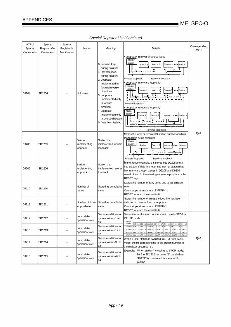
App - 49
MELSEC-Q APPENDICES
Special Register List (Continue)
ACPU
Special
Conversion
Special
Register after
Conversion
Special
Register for
Modification
Name Meaning Details Corresponding
CPU
D9204 SD1204 Link state
0: Forward loop,
during data link
1: Reverse loop,
during data link
2: Loopback
implemented in
forward/reverse
directions
3: Loopback
implemented only
in forward
direction
4: Loopback
implemented only
inreverse direction
5: Data link disabled
• Loopback in forward/reverse loops Master station
Station 1 Station 2 Station 3 Station n
Forward loopback Reverse loopback • Loopback in forward loop only
Master
stationStation 1 Station 2 Station 3 Station n
Forward loopback • Loopback in reverse loop only
Master
stationStation 1 Station 2 Station 3 Station n
Reverse loopback
D9205 SD1205
Station
implementing
loopback
Station that
implemented forward
loopback
D9206 SD1206
Station
implementing
loopback
Station that
implemented reverse
loopback
Stores the local or remote I/O station number at which
loopback is being executed. Master
stationStation 1 Station 2 Station 3 Station n
Forward loopback Reverse loopback In the above example, 1 is stored into D9205 and 3
into D9206. If data link returns to normal status (data
link in forward loop), values in D9205 and D9206
remain 1 and 3. Reset using sequence program or the
RESET key.
D9210 SD1210 Number of
retries
Stored as cumulative
value
Stores the number of retry times due to transmission
error.
Count stops at maximum of "FFFFH" .
RESET to return the count to 0.
D9211 SD1211 Number of times
loop selected
Stored as cumulative
value
Stores the number of times the loop line has been
switched to reverse loop or loopback.
Count stops at maximum of "FFFFH".
RESET to return the count to 0.
QnA
D9212 SD1212 Local station
operation state
Stores conditions for
up to numbers 1 to
16
D9213 SD1213 Local station
operation state
Stores conditions for
up to numbers 17 to
32
D9214 SD1214 Local station
operation state
Stores conditions for
up to numbers 33 to
48
D9215 SD1215 Local station
operation state
Stores conditions for
up to numbers 49 to
64
Stores the local station numbers which are in STOP or
PAUSE mode.
SD1212
SD1213
SD1214
SD1215
b15 b14 b13 b12 b11 b10 b9 b8 b7 b6 b5 b4 b3 b2 b1 b0
L16 L15 L14 L13 L12 L11
L32 L31 L30 L29 L28 L27
L48 L47 L46 L45 L44 L43
L64 L63 L62 L61 L60 L59
L26
L42
L58
L25
L41
L57
L24
L40
L56
L23
L39
L55
L22
L38
L54
L21
L37
L53
L20
L36
L52
L19
L35
L51
L18
L34
L50
L17
L33
L49
L10 L9 L8 L7 L6 L5 L4 L3 L2 L1
BitDevice number
When a local station is switched to STOP or PAUSE
mode, the bit corresponding to the station number in
the register becomes "1".
Example: When station 7 switches to STOP mode,
bit 6 in SD1212 becomes "1" , and when
SD1212 is monitored, its value is "64
(40H)".
QnA

App - 50
MELSEC-Q APPENDICES
Special Register List (Continue)
ACPU
Special
Conversion
Special
Register after
Conversion
Special
Register for
Modification
Name Meaning Details Corresponding
CPU
D9216 SD1216
Stores conditions
for up to numbers
1 to 16
D9217 SD1217
Stores conditions
for up to numbers
17 to 32
D9218 SD1218
Stores conditions
for up to numbers
33 to 48
D9219 SD1219
Local station
error detect
state
Stores conditions
for up to numbers
49 to 64
Stores the local station numbers which are in error.
SD1216
SD1217
SD1218
SD1219
b15 b14 b13 b12 b11 b10 b9 b8 b7 b6 b5 b4 b3 b2 b1 b0
L16 L15 L14 L13 L12 L11
L32 L31 L30 L29 L28 L27
L48 L47 L46 L45 L44 L43
L64 L63 L62 L61 L60 L59
L26
L42
L58
L25
L41
L57
L24
L40
L56
L23
L39
L55
L22
L38
L54
L21
L37
L53
L20
L36
L52
L19
L35
L51
L18
L34
L50
L17
L33
L49
L10 L9 L8 L7 L6 L5 L4 L3 L2 L1
BitDevice number
If a local station detects an error, the bit corresponding to
the station number becomes "1".
Example: When station 6 and 12 detect an error, bits 5
and 11 in SD1216 become "1", and when
SD1216 is monitored, its value is "2080
(820H)".
D9220 SD1220
Stores conditions
for up to numbers
1 to 16
D9221 SD1221
Stores conditions
for up to numbers
17 to 32
D9222 SD1222
Stores conditions
for up to numbers
33 to 48
D9223 SD1223
Local station
parameters
non-conforming;
remote I/O
station I/O
allocation error
Stores conditions
for up to numbers
49 to 64
Stores the local station numbers which contain
mismatched parameters or of remote station numbers for
which incorrect I/O assignment has been made.
SD1220
SD1221
SD1222
SD1223
b15 b14 b13 b12 b11 b10 b9 b8 b7 b6 b5 b4 b3 b2 b1 b0
L16 L15 L14 L13 L12 L11
L32 L31 L30 L29 L28 L27
L48 L47 L46 L45 L44 L43
L64 L63 L62 L61 L60 L59
L26
L42
L58
L25
L41
L57
L24
L40
L56
L23
L39
L55
L22
L38
L54
L21
L37
L53
L20
L36
L52
L19
L35
L51
L18
L34
L50
L17
L33
L49
L10 L9 L8 L7 L6 L5 L4 L3 L2 L1
BitDevice number
If a local station acting as the master station of tier three
detects a parameter error or a remote station contains an
invalid I/O assignment, the bit corresponding to the
station number becomes "1".
Example: When local station 5 and remote I/O station
14 detect an error, bits 4 and 13 in SD1220
become "1" , and when SD1220 is monitored,
its value is "8208 (2010H) " .
D9224 SD1224
Stores conditions
for up to numbers
1 to 16
D9225 SD1225
Stores conditions
for up to numbers
17 to 32
D9226 SD1226
Stores conditions
for up to numbers
33 to 48
D9227 SD1227
Local station
and remote I/O
station initial
communications
underway
Stores conditions
for up to numbers
49 to 64
Stores the local or remote station numbers while they are
communicating the initial data with their relevant master
station.
SD1224
SD1225
SD1226
SD1227
b15 b14 b13 b12 b11 b10 b9 b8 b7 b6 b5 b4 b3 b2 b1 b0L/R16
L/R15
L/R14
L/R13
L/R12
L/R11
L/R10
L/R9
L/R8
L/R7
L/R6
L/R5
L/R4
L/R3
L/R2
L/R1
L/R32
L/R31
L/R30
L/R29
L/R28
L/R27
L/R26
L/R25
L/R24
L/R23
L/R22
L/R21
L/R20
L/R19
L/R18
L/R17
L/R48
L/R47
L/R46
L/R45
L/R44
L/R43
L/R42
L/R41
L/R40
L/R39
L/R38
L/R37
L/R36
L/R35
L/R34
L/R33
L/R64
L/R63
L/R62
L/R61
L/R60
L/R59
L/R58
L/R57
L/R56
L/R55
L/R54
L/R53
L/R52
L/R51
L/R50
L/R49
BitDevice number
The bit corresponding to the station number which is
currently communicating the initial settings becomes "1" .
Example: When stations 23 and 45 are communicating,
bit 6 of SD1225 and bit 12 of SD1226
become "1", and when SD1225 is monitored,
its value is "64 (40H)", and when SD1226 is
monitored, its value is "4096 (1000H)"
D9228 SD1228
Stores conditions
for up to numbers
1 to 16
D9229 SD1229
Stores conditions
for up to numbers
17 to 32
D9230 SD1230
Stores conditions
for up to numbers
33 to 48
D9231 SD1231
Local station
and remote I/O
station error
Stores conditions
for up to numbers
49 to 64
Stores the local or remote station numbers which are in
error.
SD1228
SD1229
SD1230
SD1231
b15 b14 b13 b12 b11 b10 b9 b8 b7 b6 b5 b4 b3 b2 b1 b0L/R16
L/R15
L/R14
L/R13
L/R12
L/R11
L/R10
L/R9
L/R8
L/R7
L/R6
L/R5
L/R4
L/R3
L/R2
L/R1
L/R32
L/R31
L/R30
L/R29
L/R28
L/R27
L/R26
L/R25
L/R24
L/R23
L/R22
L/R21
L/R20
L/R19
L/R18
L/R17
L/R48
L/R47
L/R46
L/R45
L/R44
L/R43
L/R42
L/R41
L/R40
L/R39
L/R38
L/R37
L/R36
L/R35
L/R34
L/R33
L/R64
L/R63
L/R62
L/R61
L/R60
L/R59
L/R58
L/R57
L/R56
L/R55
L/R54
L/R53
L/R52
L/R51
L/R50
L/R49
BitDevice number
The bit corresponding to the station number with the error
becomes "1" .
Example: When local station 3 and remote I/O station
14 have an error, bits 2 and 13 of D9228
become "1", and when SD1228 is monitored,
its value is "8196 (2004H)".
QnA
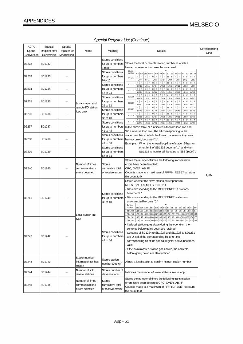
App - 51
MELSEC-Q APPENDICES
Special Register List (Continue)
ACPU
Special
Conversion
Special
Register after
Conversion
Special
Register for
Modification
Name Meaning Details Corresponding
CPU
D9232 SD1232
Stores conditions
for up to numbers
1 to 8
D9233 SD1233
Stores conditions
for up to numbers
9 to 16
D9234 SD1234
Stores conditions
for up to numbers
17 to 24
D9235 SD1235
Stores conditions
for up to numbers
25 to 32
D9236 SD1236
Stores conditions
for up to numbers
33 to 40
D9237 SD1237
Stores conditions
for up to numbers
41 to 48
D9238 SD1238
Stores conditions
for up to numbers
49 to 56
D9239 SD1239
Local station and
remote I/O station
loop error
Stores conditions
for up to numbers
57 to 64
Stores the local or remote station number at which a
forward or reverse loop error has occurred
SD1232
b15 b14 b13 b12 b11 b10 b9 b8 b7 b6 b5 b4 b3 b2 b1 b0
L/R8 L/R7 L/R6 L/R5 L/R4 L/R3 L/R2 L/R1
SD1233L/R16 L/R15 L/R14 L/R13 L/R12 L/R11 L/R10 L/R9
SD1234L/R24 L/R23 L/R22 L/R21 L/R20 L/R19 L/R18 L/R17
SD1235L/R32 L/R31 L/R30 L/R29 L/R28 L/R27 L/R26 L/R25
SD1236L/R40 L/R39 L/R38 L/R37 L/R36 L/R35 L/R34 L/R33
SD1237L/R48 L/R47 L/R46 L/R45 L/R44 L/R43 L/R42 L/R41
SD1238L/R56 L/R55 L/R54 L/R53 L/R52 L/R51 L/R50 L/R49
SD1239L/R64 L/R63 L/R62 L/R61 L/R60 L/R59 L/R58 L/R57
BitDevice number
R F R F R F R F R F R F R F R F
R F R F R F R F R F R F R F R F
R F R F R F R F R F R F R F R F
R F R F R F R F R F R F R F R F
R F R F R F R F R F R F R F R F
R F R F R F R F R F R F R F R F
R F R F R F R F R F R F R F R F
R F R F R F R F R F R F R F R F
In the above table, "F" indicates a forward loop line and
"R" a reverse loop line .The bit corresponding to the
station number at which the forward or reverse loop error
has occurred, becomes "1".
Example: When the forward loop line of station 5 has an
error, bit 8 of SD1232 become "1", and when
SD1232 is monitored, its value is "256 (100H)".
D9240 SD1240
Number of times
communications
errors detected
Stores
cumulative total
of receive errors
Stores the number of times the following transmission
errors have been detected:
CRC, OVER, AB. IF
Count is made to a maximum of FFFFH. RESET to return
the count to 0.
D9241 SD1241
Stores conditions
for up to numbers
33 to 48
D9242 SD1242
Local station link
type
Stores conditions
for up to numbers
49 to 64
Stores whether the slave station corresponds to
MELSECNET or MELSECNET11.
• Bits corresponding to the MELSECNET 11 stations
become "1."
• Bits corresponding to the MELSECNET stations or
unconnected become "0."
SD1202
SD1203
SD1241
SD1242
b15 b14 b13 b12 b11 b10 b9 b8 b7 b6 b5 b4 b3 b2 b1 b0
L16 L15 L14 L13 L12 L11
L32 L31 L30 L29 L28 L27
L48 L47 L46 L45 L44 L43
L64 L63 L62 L61 L60 L59
L26
L42
L58
L25
L41
L57
L24
L40
L56
L23
L39
L55
L22
L38
L54
L21
L37
L53
L20
L36
L52
L19
L35
L51
L18
L34
L50
L17
L33
L49
L10 L9 L8 L7 L6 L5 L4 L3 L2 L1
BitDevice number
• If a local station goes down during the operation, the
contents before going down are retained.
Contents of SD1224 to SD1227 and SD1228 to SD1231
are ORed. If the corresponding bit is "0", the
corresponding bit of the special register above becomes
valid.
• If the own (master) station goes down, the contents
before going down are also retained.
D9243 SD1243
Station number
information for host
station
Stores station
number (0 to 64) Allows a local station to confirm its own station number
D9244 SD1244 Number of link
device stations
Stores number of
slave stations Indicates the number of slave stations in one loop.
D9245 SD1245
Number of times
communications
errors detected
Stores
cumulative total
of receive errors
Stores the number of times the following transmission
errors have been detected: CRC, OVER, AB. IF
Count is made to a maximum of FFFFH. RESET to return
the count to 0.
QnA

App - 52
MELSEC-Q APPENDICES
Special Register List (Continue)
ACPU
Special
Conversion
Special
Register after
Conversion
Special
Register for
Modification
Name Meaning Details Corresponding
CPU
D9248 SD1248
Stores conditions
for up to numbers 1
to 16
D9249 SD1249
Stores conditions
for up to numbers
17 to 32
D9250 SD1250
Stores conditions
for up to numbers
33 to 48
D9251 SD1251
Local station
operation
state
Stores conditions
for up to numbers
49 to 64
Stores the local station number which is in STOP or PAUSE
mode.
SD1248
SD1249
SD1250
SD1251
b15 b14 b13 b12 b11 b10 b9 b8 b7 b6 b5 b4 b3 b2 b1 b0
L16 L15 L14 L13 L12 L11
L32 L31 L30 L29 L28 L27
L48 L47 L46 L45 L44 L43
L64 L63 L62 L61 L60 L59
L26
L42
L58
L25
L41
L57
L24
L40
L56
L23
L39
L55
L22
L38
L54
L21
L37
L53
L20
L36
L52
L19
L35
L51
L18
L34
L50
L17
L33
L49
L10 L9 L8 L7 L6 L5 L4 L3 L2 L1
BitDevice number
The bit corresponding to the station number which is in
STOP or PAUSE mode, becomes "1".
Example: When local stations 7 and 15 are in STOP mode,
bits 6 and 14 of SD1248 become "1", and when
SD1248 is monitored, its value is "16448
(4040H)".
D9252 SD1252
Stores conditions
for up to numbers 1
to 16
D9253 SD1253
Stores conditions
for up to numbers
17 to 32
D9254 SD1254
Stores conditions
for up to numbers
33 to 48
D9255 SD1255
Local station
error
conditions
Stores conditions
for up to numbers
49 to 64
Stores the local station number other than the host, which is
in error.
SD1252
SD1253
SD1254
SD1255
b15 b14 b13 b12 b11 b10 b9 b8 b7 b6 b5 b4 b3 b2 b1 b0
L16 L15 L14 L13 L12 L11
L32 L31 L30 L29 L28 L27
L48 L47 L46 L45 L44 L43
L64 L63 L62 L61 L60 L59
L26
L42
L58
L25
L41
L57
L24
L40
L56
L23
L39
L55
L22
L38
L54
L21
L37
L53
L20
L36
L52
L19
L35
L51
L18
L34
L50
L17
L33
L49
L10 L9 L8 L7 L6 L5 L4 L3 L2 L1
BitDevice number
The bit corresponding to the station number which is in error,
becomes "1".
Example: When local station 12 is in error, bit 11 of SD1252
becomes "1", and when SD1252 is monitored, its
value is "2048 (800H) ".
QnA
(11) Fuse blown module
Number Name Meaning Explanation
Set by
(When
set)
Corresponding
ACPU
D9
Corresponding
CPU
SD1300 D9100
SD1301 D9101
SD1302 D9102
SD1303 D9103
SD1304 D9104
SD1305 D9105
SD1306 D9106
SD1307 D9107
SD1308 New
SD1309
to
SD1330
New to New
SD1331
Fuse blown
module
Bit pattern in units
of 16 points,
indicating the
modules whose
fuses have blown
0: No blown fuse
1: Blown fuse
present
• The numbers of output modules whose fuses have blown are
input as a bit pattern (in units of 16 points).
(If the module numbers are set by parameter, the parameter-set
numbers are stored.)
• Also detects blown fuse condition at remote station output
modules 15 14 13 12 11 10 9 8 7 6 5 4 3 2 1 0
0 0 0 1(YC0)
0 0 0 0 0 0 0 0 0 0 01(Y80)SD1300
0 01(Y1F0) 0 0 0 0 0 0 0 0 0 01
(Y1A)SD1301 0 0
0 01
(Y1F B0)
0 0 0 0 0 0 0 0SD1331 0 001
(Y1F 30)
0
Indicates a blown fuse• Not cleared even if the blown fuse is replaced with a new one.
This flag is cleared by error resetting operation
(refer to 11.3.).
S (Error)
New
SD1350
to
SD1381
External
power supply
disconnected
module
(For future
expansion)
Bit pattern in units
of 16 points,
indicating the
modules whose
external power
supply has been
disconnected
0: External power
supply
disconnected
1: External power
supply is not
disconnected
The module number (in units of 16 points) whose external power
supply has been disconnected is input as a bit pattern.
(If the module numbers are set by parameter, the parameter-set
numbers are used.) 15 14 13 12 11 10 9 8 7 6 5 4 3 2 1 0
SD1350
SD1351
0 0 0 1 0 0 0 0 0 0 0 0 0 0 01
0 01 0 0 0 0 0 0 0 0 0 010 0
SD1381 0 0 1 0 0 0 0 0 0 0 00 00 10
Indicates a blown fuse
S (Error) New QCPU

App - 53
MELSEC-Q APPENDICES
Special Register List (Continue)
(12) I/O module verification
Number Name Meaning Explanation
Set by
(When
set)
Corresponding
ACPU
D9
Corresponding
CPU
SD1400 D9116
SD1401 D9117
SD1402 D9118
SD1403 D9119
SD1404 D9120
SD1405 D9121
SD1406 D9122
SD1407 D9123
SD1408 New
SD1409
to
SD1430
New to New
SD1431
I/O module
verification
error
Bit pattern, in
units of 16 points,
indicating the
modules with
verification errors.
0: No I/O
verification
errors
1: I/O verification
error present
• When the power is turned on, the module numbers of the I/O
modules whose information differs from the registered I/O module
information are set in this register (in units of 16 points).
(If the I/O numbers are set by parameter, the parameter-set
numbers are stored.)
• Also detects I/O module information 15 14 13 12 11 10 9 8 7 6 5 4 3 2 1 0
0 0 0 0 0 0 0 0 0 0 0 0 0D9116
0 0 0 0 0 0 0 0 0 0 0D9117 0 0
0 0 0 0 0 0 0 0 0D9123 0 000
0 0
00
001
( )X Y1FE0
1( )
1( )X Y
190
X Y0
Indicates an I/O module verification error • Not cleared even if the blown fuse is replaced with a new one.
This flag is cleared by error resetting operation
(refer to 11.3.).
S (Error)
New
(13) For redundant systems (Host system CPU information 1) for Q4AR only
SD1510 to SD1599 are only valid for redundant systems. They are all set to 0 for
standalone systems.
Number Name Meaning Explanation Set by
(When set)
Corresponding
ACPU
D9
Corresponding
CPU
SD1500
SD1501 Basic period
Basic period
tome
• Set the basic period (1 second units) use for the process
control instruction using floating point data.
SD1501 SD1500Floating points data = U New
SD1502
Process control
instruction detail
error code
Process control
instruction detail
error code
• Shows the detailed error contents for the error that occurred
in the process control instruction
S (Error
occurrence) New
SD1503
Process control
instruction
generated error
location
Process control
instruction
generated error
location
• Shows the error process block that occurred in the process
control instruction.
S (Error
occurrence) New
SD1512
Operation mode
during CPU start
up
Hot start switch
power out time
• Shows the power out time (S) during the automatic switch
from hot start to initial start in the operation mode when the
CPU is started up.
S (Initial) New
SD1590 Switch request
network No.
Request origin
network No.
• Stores the request origin at work No. when the SM1590 is
turned on.
S (Error
occurrence) New
1 Stores the host system CPU information.

App - 54
MELSEC-Q APPENDICES
Special Register List (Continue)
(14) For redundant systems (Other system CPU information 1) for Q4AR only SD1600 to SD1659 is only valid during the back up mode for redundant systems, and refresh cannot be done when in the separate mode. When a standalone system SD1600 to SD1699 are all 0.
Number Name Meaning Explanation Set by
(When set)
Corresponding
ACPU
SD 2
Corresponding
CPU
SD1600 Diagnosis error Diagnosis error
No.
• Stores as BIN code the error No. of the error that occurred during the other system CPU diagnosis.
• Stores the latest error currently occurring.
S (Each
END) SD0
SD1601
SD1602
SD1603
Diagnosis error
occurrence
time
Diagnosis error
occurrence time
• SD1600 stores the updated date and time. • Stores each of the BCD two digits. • Refer to SD1 to SD3 for the storage status.
(SD1 SD1601, SD2 SD1602, SD3 SD1603)
S (Each
END) SD1 to SD3
SD1604
Error
information
classification
Error
information
classification
• Stores the error comment information/individual information
classification code.
• Refer to SD4 for the storage status.
S (Each
END) SD4
SD1605
SD1606
SD1607
SD1608
SD1609
SD1610
SD1611
SD1612
SD1613
SD1614
SD1615
Error common
information
Error common
information
• Stores the common information for the error code.
• Refer to SD5 to SD15 for the storage status.
(SD5 SD1605, SD6 SD1606, SD7 SD1607,
SD8 SD1608, SD9 SD1609, SD10 SD1610,
SD11 SD1611, SD12 SD1612, SD13 SD1613,
SD14 SD1614, SD15 SD1615)
S (Each
END) SD5 to SD15
SD1616
SD1617
SD1618
SD1619
SD1620
SD1621
SD1622
SD1623
SD1624
SD1625
SD1626
Error individual
information
Error individual
information
• Stores the individual information for the error code Refer to
SD16 to SD26 for the storage status.
(SD16 SD1616, SD17 SD1617, SD18 SD1618,
SD19 SD1619, SD20 SD1620, SD21 SD1621,
SD22 SD1622, SD23 SD1623, SD24 SD1624,
SD25 SD1625, SD26 SD1626)
S (Each
END) SD16 to SD26
SD1650 Switch status CPU switch
status
• Stores the CPU switch status.
• Refer to SD200 for the storage status. (SD1650 SD200)
S (Each
END) SD200
SD1651 LED status CPU-LED status
• Stores the CPU's LED status.
• Shows 0 when turned off, 1 when turned on, and 2 when
flashing.
• Refer to SD201 for the storage status. (SD1651 SD201)
S (Each
END) SD201
SD1653 CPU operation
status
CPU operation
status
• Stores the CPU operation status. Refer to SD203 for the
storage status. (SD1653 SD203)
S (Each
END) SD203
Q4AR
1 Stores other system CPU self-diagnostic information and system information.
2 Shows the special register (SD ) for the host system CPU.
(15) For redundant systems (Trucking) for Q4AR only SD1700 to SD1799 is valid only for redundant systems. These are all 0 for
standalone systems.
Number Name Meaning Explanation Set by
(When set)
Corresponding
ACPU
SD 2
Corresponding
CPU
SD1700 Trucking error
detection count
Trucking error
detection count • Make it the trucking error detection +1.
Error
occurrence New Q4AR
2 Shows the special register (SD ) for the host system CPU.

App - 55
MELSEC-Q APPENDICES
APPENDIX 3 List of Interrupt Pointer Nos. & Interrupt Factors
I No. Interrupt Factors Priority
Ranking I No. Interrupt factors
Priority Ranking
I0 1st point 237 I32*2 Errors that stop operation 1
I1 2nd point 238 I33 Vacant ——
I2 3rd point 239
I3 4th point 240
I4 5th point 241
I34
UNIT VERIFY ERR.
FUSE BREAK OFF
SP. UNIT ERROR
2
I5 6th point 242
I6 7th point 243
I7 8th point 244
I8 9th point 245
I35
OPERATION ERROR
SFCP OPE. ERROR
SFCP ECE. ERROR
EX. POWER OFF
3
I9 10th point 246
I10 11th point 247 I36
ICM. OPE ERROR
FILE OPE. ERROR 4
I11 12th point 248 I37 Vacant ——
I12 13th point 249 I38 PRG. TIME OVER 5
I13 14th point 250
I14 15th point 251 I39
Error factor*3*4,
CHK instruction execution
Anunciator detection 6
I15
A1SI61 interrupt
module factor
16th point 252
I16 1st point 224
I17 2nd point 225
I18 3rd point 226
I40 to
I49 —— Vacant ——
I19 4th point 227
I20 5th point 228
I21 6th point 229
I22 7th point 230
I23 8th point 231
I24 9th point 232
I25 10th point 234
I26 11th point 235
I27
Sequence start
generator module
factor*1
12th point 236
I28 100ms 256
I29 40ms 255
I30 20ms 254
I31
Internal timer factor
*2
10ms 253
I50 to
I255
Intelligent-function
module factor *5
Specifies which intelligent
function module is used
with parameters.
18 to 223
REMARK
1) *1 : 1st to 12th points are allocated in order, beginning from the sequence start generator module installed closest to the QCPU.
2) *2 :The internal times shown are the default setting times. These times can be designated in 0.5 ms units through a 0.5 ms to 1000 ms range by the GPPW(PLC system settings in the PLC parameter setting).
3) *3 :When an error interruption with "I32 (error that stops operation)" occurs, the QCPU is not stopped until I32 processing is completed.
4) *4 :Execution of error interruptions is prohibited for the interrupt pointer Nos. I32 to I39 when the power is turned on and during a QCPU reset. When using interrupt pointer Nos. I32 to I39, set the interruption permitted status by using the IMASK instruction.

App - 56
MELSEC-Q APPENDICES
MEMO

Index - 1
INDEX
[A] Accuracy of initial scan time.......................4-16 Accuracy of scan time................................4-18 Annunciator (F).........................................10-12 ASCII code .................................................4-50 ATA card.....................................................6-10 Auto mode ..................................................5- 3
[B]
B (Link relay) ............................................10-17
Base mode .................................................5- 3
BCD (Binary coded decimal) .....................4-47
BIN (Binary code) .......................................4-45
BL (SFC block device) .............................10-58
Boot operation ............................................6-13 [C]
C (Counter)...................................................10-24
Catalog PLC memory ....................................6-14
Character string..............................................4-50
Clock function.................................................7- 9
Precision .....................................................7-11
Year 2000 problems...................................7-11
Common pointer...........................................10-54
Concept of I/O assignment .............................5- 7
Concept of I/O assignment using GPPW......5-10
Constant scan ................................................7- 2
Constants .....................................................10-61
Counter (C)...................................................10-24
Count processing .....................................10-24
Maximum counting speed........................10-25 [D]
D (Data register)...........................................10-28
Data register (D)...........................................10-28
Data stored on the memory card...................6- 4
Decimal constants (K)..................................10-61
Device initial value ......................................10- 69
Device list .....................................................10- 1
Direct access input.......................................10- 6
Direct access output ....................................10- 9
Direct mode ....................................................4-41
Drive No..........................................................6- 5
Duty ..............................................................10-25
DX (Direct access input) ..............................10- 6
DY (Direct access output)............................10- 9
[E]
E (Real numbers).........................................10-62
Edge relay(V) ...............................................10-16
END processing.............................................4-34
Execute type ..................................................4-10
Execution time measurement........................7-32
Execution time of the low-speed execution type
program..........................................................4-19
Extension .......................................................6- 2
6- 4
[F] F (Annunciator) ............................................10-12
Failure history ................................................7-57
FD (Function register)..................................10-31
File register ..................................................10-43
Access method ........................................10-44
Designation method.................................10-49
Registering ...............................................10-45
File size ..........................................................6-18
Fixed scan execution type program..............4-31
Flash card ......................................................6-10
Floating decimal point data ...........................4-28
Function device (FX, FY, FD)......................10-31
FX (Function input) ......................................10-31
FY (Function output)....................................10-31
[G] Global device ...............................................10-63
GPPW ............................................................A-13
[H] H (Hexadecimal constants) .........................10-61
HEX (Hexadecimal) .......................................4-46
Hexadecimal constants (H) .........................10-61
High-speed retentive timer (ST)..................10-21
High-speed timer (T)....................................10-20

Index - 2
[I] I (Interrupt pointer) .......................................10-56
I/O No. designation device (Un) ..................10-59
Index register (Z)..........................................10-39
Initial execution monitor time .........................4-16
Initial execution type program........................4-15
Initial scan time...............................................4-16
Input response speed ....................................7-20
Intelligent function module device (U \G ). 10-38
Internal relay (M) ..........................................10-10
Internal system device .................................10-31
Internal user device......................................10- 3
Interrupt pointer (I) .......................................10-56
Interrupt program ...........................................4- 6
[J] J (Network designation device) ...................10-58
J \B (Link relay) ...................................10-35
J \SB (Link special relay) ....................10-35
J \SW (Link special register)...............10-35
J \W (Link register) ..............................10-35
J \X (Link input) ...................................10-35
J \Y (Link output) .................................10-35
[K] K (Decimal constants)..................................10-61
[L] L (Latch relay) ..............................................10-11
Latch function ..................................................7- 5
Latch relay (L) ..............................................10-11
LED diaplay....................................................7-62
Link direct device .........................................10-35
Link register ..................................................10-29
Link relay ......................................................10-17
List of Interrupt factors .................................10-57
App-55
Local device .................................................10-63
Low-speed END processing..........................4-23
Low-speed execution monitor time................4-24
Low-speed execution type program ..............4-19
Low-speed retentive timer (ST) ...................10-21
Low-speed scan timer....................................4-23
Low-speed timer (T).....................................10-19
[M] M (Internal relay)..........................................10-10
Macro instruction argument device (VD) ....10-60
Main routine program ....................................4- 3
Memory card..................................................6-10
Monitor condition setting................................7-22
Monitoring the local devices ..........................7-27
[N] N (Nesting) ...................................................10-52
[O] Output (Y).....................................................10- 8
[P] P (Pointer) ....................................................10-53
Password .......................................................7-58
PLOW instruction...........................................4-14
POFF instruction............................................4-14
Precautions for the use of device initial values ...10-71
Precautions when using timers ...................10-23
Priority of LED................................................7-64
Procedure for using device initial values ....10-70
Processing at annunciator OFF ..................10-14
Processing at annunciator ON ....................10-12
Program construction ....................................1- 4
Program execute type ...................................4-10
Program memory...........................................6- 6
Program monitor list ......................................7-32
PSCAN instruction.........................................4-14
PSTOP instruction .........................................4-14
Purpose of I/O assignment............................5- 9
Purpose of I/O assignment using GPPW .....5- 9
[Q] QCPU.............................................................A-13
QnCPU...........................................................A-13
QnHCPU ........................................................A-13
Index - 3
[R] R (File register).............................................10-43
Reading from the time data ...........................7-11
Real numbers (E) ...........................................4-48
10-62
Refresh input ................................................10- 6
Refresh mode.................................................4-38
Refresh output..............................................10- 9
Remote latch clear .........................................7-18
Remote operation...........................................7-12
Remote PAUSE .............................................7-15
Remote RESET..............................................7-17
Remote RUN/STOP.......................................7-12
Retentive timer (OUT ST ) .......................10-21
RUN state.......................................................4-35
[S] S (Step relay) ...............................................10-18
SB (Special link relay) ..................................10-18
Scan execution type program........................4-17
Scan time........................................................4-18
SD (Special register) ....................................10-34
SD415 (2n ms clock setting)..........................8- 9
SD520, SD521 (Scan time: present value) ...4-18
SD522, SD523 (Initial scan time) ..................4-16
SD524, SD525 (Scan time: Maximum value).......4-18
SD526, SD527 (Scan time: Minimum value)........4-18
SD528, SD529 (Low-speed scan time: Present value)
....................................................................................4-23
SD530, SD531 (Low-speed scan time: Initial value)
...............................................................................4-23
SD532, SD533 (Low-speed scan time: Minimum value)
....................................................................................4-23
SD534, SD535 (Low-speed scan time: Maximum
value)...............................................................4-23
Self-diagnosis function...................................7-52
Sequence program ........................................4- 1
Setting range in the internal user device.....10- 3
Setting the number of stages.........................5- 2
SFC block device (BL) .................................10-58
SFC transition device (TR) ..........................10-58
Single precision floating decimal point data......4-48
Size (File capacity) .........................................6- 2
SM (Special relay)........................................10-33
SM415 (2n ms clock) .....................................8- 9
Special link register (SW) ............................10-30
Special link relay (SB)..................................10-18
Special register (SD)....................................10-34
Special relay (SM)........................................10-33
SRAM card.....................................................6-10
ST (Retentive timer: OUT ST ) ................10-21
Stand-by type program..................................4-25
Standard RAM ...............................................6- 9
Standard ROM...............................................6- 8
Step relay (S) ...............................................10-18
Subroutine program.......................................4- 4
SW (Special link register) ............................10-30
Switch setting of intelligent function module.7-21
System protect...............................................7-58
[T] T (Timer) ......................................................10-19
Timer (T) ......................................................10-19
Accuracy...................................................10-22
Processing ...............................................10-22
TR (SFC transition device) ..........................10-58
[U] U (I/O No. designation device) ....................10-59
U \G (Intelligent function module device) ..10-38
User memory .................................................6- 3
[V] V (Edge relay) ..............................................10-16
VD (Macro instruction argument device) ....10-60
[W] W (Link register) ..........................................10-29
Watchdog timer..............................................7-50
WDT (Watchdog timer)..................................7-50
Write during RUN...........................................7-28
7-30
7-48
Writing to the time data .................................7- 9
[X] X (Input) .......................................................10- 5
[Y] Y (Output).....................................................10- 8
Year 2000 problems ......................................7-11
[Z] Z (Index register) .........................................10-39
ZR (Serial number access format of file register)
......................................................................10-49

HEADQUARTERS
MITSUBISHI ELECTRIC EUROPEEUROPE B.V.German BranchGothaer Straße 8D-40880 RatingenPhone: +49 (0) 21 02 / 486-0Fax: +49 (0) 21 02 / 4 86-1 12E mail: [email protected]
MITSUBISHI ELECTRIC ITALYEUROPE B.V.ITALIAN BRANCHCentro Dir. Colleoni Pal. Perseo - Ingr. 2Via Paracelso 12I-20041 Agrate Brianza (MI)Phone: +39 039 6053 1Fax: +39 039 6053 312E mail: [email protected]
MITSUBISHI ELECTRIC SPAINEUROPE B.V.SPANISH BRANCHPol. Ind. Can MagiCalle Joan Buscallá, 2–4E-08190 Sant Cugat del VallésPhone: +34 (9) 3 / 565 31 60Fax: +34 (9) 3 / 589 15 79E mail: [email protected]
MITSUBISHI ELECTRIC UKEUROPE B.V.UK BranchTravellers LaneGB-Hatfield Herts. AL10 8 XBPhone: +44 (0) 1707 / 27 61 00Fax: +44 (0) 1707 / 27 86 95
MITSUBISHI ELECTRIC JAPANCORPORATION2-2-3 Marunouchi Chiyoda-KuTokyo 100-8310Phone: +81 (0) 3 / 32 18 31 76Fax: +81 (0) 3 / 32 18 24 22
MITSUBISHI ELECTRIC USAAUTOMATION INC.500 Corporate Woods ParkwayVernon Hills, IL 60061Phone: +1 847 / 478 2100Fax: +1 847 / 478 2283
EUROPEAN REPRESENTATIVES
GEVA GmbH AUSTRIAWiener Straße 89A-2500 BadenPhone: +43 (0) 2252 / 85 55 20Fax: +43 (0) 2252 / 488 60E mail: [email protected]
GETRONICS NV/SA BELGIUMPontbeeklaan 43B-1731 ZellikPhone: +32 (0) 2 / 467 17 11Fax: +32 (0) 2 / 467 17 00E mail: [email protected]
TELECON CO. BULGARIA4, A. Ljapchev Blvd.BG-1756 SofiaPhone: +359 92 / 97 44 05 8Fax: +359 92 / 97 44 06 1E mail: —
AutoCont s.r.o. CZECHIANemocnicni 12CZ-70100 Ostrava 1Phone: +420 (0) 69 / 615 21 11Fax: +420 (0) 69 / 615 21 12E mail: [email protected]
louis poulsen DENMARKGeminivej 32DK-2670 GrevePhone: +45 (0) 43 / 95 95 95Fax: +45 (0) 43 / 95 95 91E mail: [email protected]
UTU ELEKTROTEHNIKA AS ESTONIALaki 12EEE-10621 TallinnPhone: +372 6 / 51 72 80Fax: +372 6 / 51 72 88E mail: [email protected]
Beijer Electronics OY FINLANDElannontie 5FIN-01510 VantaaPhone: +358 (0) 9 / 615 20 11Fax: +358 (0) 9 / 615 20 500E mail: [email protected]
IP Systèmes FRANCE8, Rue du Colonel ChambonnetF-69672 Lyon Bron CedexPhone: +33 (0) 4 / 72 14 18 00Fax: +33 (0) 4 / 72 14 18 01E mail: [email protected]
MITSUBISHI ELECTRIC IRELANDEUROPE B.V. – Irish BranchWestgate Business ParkIRL-Dublin 24Phone: +353 (0) 1 / 419 88 00Fax: +353 (0) 1 / 419 88 90
EUROPEAN REPRESENTATIVES
Getronics bv NETHERLANDSIndustrial AutomationDonauweg 10NL-1043 AJ-AmsterdamPhone: +31 (0) 20 / 586 14 11Fax: +31 (0) 20 / 586 19 27E mail: [email protected]
Beijer Electronics A/S NORWAYTeglverksveien 1N-3002 DrammenPhone: +47 (0) 32 / 24 30 00Fax: +47 (0) 32 / 84 85 77E mail: [email protected]
MPL Technology SP. Z.o.o POLANDul. Wroclawska 53PL-30011 KrakówPhone: +48 (0) 12 / 632 28 85Fax: +48 (0) 12 / 632 47 82E mail: [email protected]
Sirius Trading & Services srl ROMANIABd. Ghica nr. 112, Bl. 41, Sc. 2RO-72335 Bucaresti 2Phone: +40 (0) 1 / 210 55 11Fax: +40 (0) 1 / 210 55 11E mail: [email protected]
ACP AUTOCOMP a.s. SLOVAKIAChulupkova 7SK-81109 BratisavaPhone: +421 (0) 7 592 2248Fax: +421 (0) 7 592 2254E mail: [email protected]
INEA d.o.o. SLOVENIALjubljanska 80SI-61230 DomzalePhone: +386 (0) 1 / 721 80 00Fax: +386 (0) 1 / 724 16 72E mail: [email protected]
Beijer Electronics AB SWEDENBox 325S-20123 MalmöPhone: +46 (0) 40 / 35 86 00Fax: +46 (0) 40 / 93 23 01E mail: [email protected]
ECONOTEC AG SWITZERLANDPostfach 282CH-8309 NürensdorfPhone: +41 (0) 1 / 838 48 11Fax: +41 (0) 1 / 838 48 12E mail: [email protected]
GTS TURKEYDarülaceze Cad., No. 43 KAT: 2TR-80270 Okmeydani-IstanbulPhone: +90 (0) 212 / 320 1640Fax: +90 (0) 212 / 320 1649E mail: [email protected]
MIDDLE EAST REPRESENTATIVES
TEXEL Electronics Ltd. ISRAELPO Box 6272IL-Netanya 42160Phone: +972 (0) 9 / 863 08 91Fax: +972 (0) 9 / 885 24 30E mail: [email protected]
EURASIAN REPRESENTATIVES
MITSUBISHI ELECTRIC RUSSIAEUROPE B.V.12/ Goncharnava St, suite 3cRUS-109240 MoscowPhone: +7 (0) 95 / 915-8602Fax: +7 (0) 95 / 915-8603E mail: —
JV-CSC Automation UKRAINE15, M. Raskovoyi St.Floor 10, Office 1010U-02002 KievPhone: +380 (4) 4 / 238 83 16Fax: +380 (4) 4 / 238 83 17E mail: [email protected]
Gothaer Strasse 8 Phone: +49 2102 486-0 Fax: +49 2102 486-717 www.mitsubishi-automation.de [email protected] Ratingen Hotline: +49 2102 1805 000-765 /-766 Faxback: +49 2102 486-485 /-790 www.mitsubishi-automation.com
INDUSTRIAL AUTOMATIONMITSUBISHI ELECTRIC EUROPE B.V.