Embed Size (px)
Citation preview
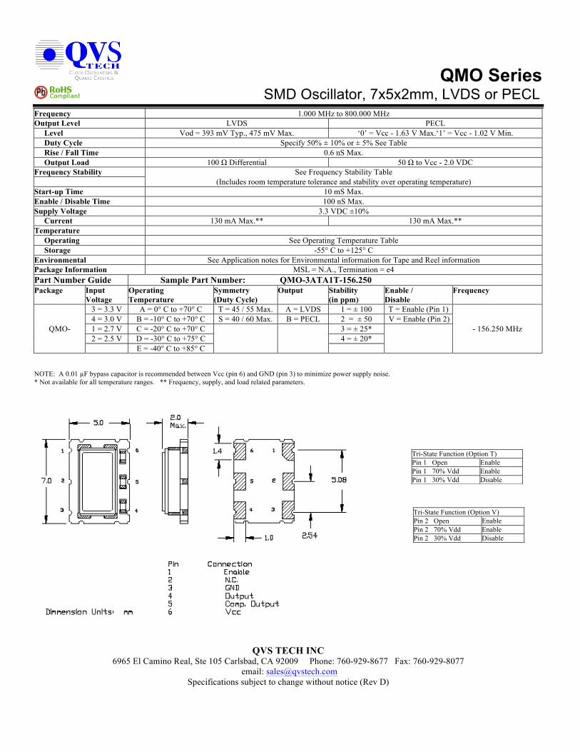
QMO Series SMD Oscillator, 7x5x2mm, LVDS or PECL
QVS TECH INC 6965 El Camino Real, Ste 105 Carlsbad, CA 92009 Phone: 760-929-8677 Fax: 760-929-8077
email: [email protected] Specifications subject to change without notice (Rev D)
Frequency 1.000 MHz to 800.000 MHz Output Level LVDS PECL Level Vod = 393 mV Typ., 475 mV Max. ‘0’ = Vcc - 1.63 V Max.‘1’ = Vcc - 1.02 V Min. Duty Cycle Specify 50% ± 10% or ± 5% See Table Rise / Fall Time 0.6 nS Max. Output Load 100 Ω Differential 50 Ω to Vcc - 2.0 VDC Frequency Stability See Frequency Stability Table (Includes room temperature tolerance and stability over operating temperature) Start-up Time 10 mS Max. Enable / Disable Time 100 nS Max. Supply Voltage 3.3 VDC ±10% Current 130 mA Max.** 130 mA Max.** Temperature Operating See Operating Temperature Table Storage -55° C to +125° C Environmental See Application notes for Environmental information for Tape and Reel information Package Information MSL = N.A., Termination = e4 Part Number Guide Sample Part Number: QMO-3ATA1T-156.250
Package Input Operating Symmetry Output Stability Enable / Frequency Voltage Temperature (Duty Cycle) (in ppm) Disable 3 = 3.3 V A = 0° C to +70° C T = 45 / 55 Max. A = LVDS 1 = ± 100 T = Enable (Pin 1) 4 = 3.0 V B = -10° C to +70° C S = 40 / 60 Max. B = PECL 2 = ± 50 V = Enable (Pin 2)
QMO- 1 = 2.7 V C = -20° C to +70° C 3 = ± 25* - 156.250 MHz 2 = 2.5 V D = -30° C to +75° C 4 = ± 20* E = -40° C to +85° C NOTE: A 0.01 µF bypass capacitor is recommended between Vcc (pin 6) and GND (pin 3) to minimize power supply noise. * Not available for all temperature ranges. ** Frequency, supply, and load related parameters.
Tri-State Function (Option T) Pin 1 Open Enable Pin 1 70% Vdd Enable Pin 1 30% Vdd Disable
Tri-State Function (Option V) Pin 2 Open Enable Pin 2 70% Vdd Enable Pin 2 30% Vdd Disable