Embed Size (px)
Citation preview
DS541 (v1.0) November 27, 2006 www.xilinx.comProduct Specification 1
© 2006 Xilinx, Inc. All rights reserved. All Xilinx trademarks, registered trademarks, patents, and disclaimers are as listed at http://www.xilinx.com/legal.htm. PowerPC is a trademark of IBM, Inc. All other trademarks are the property of their respective owners. All specifications are subject to change without notice.
Features• In-System Programmable PROM for Configuration of
Xilinx FPGAs
• Low-Power Advanced CMOS NOR FLASH Process
• Endurance of 20,000 Program/Erase Cycles
• Operation over Full Military Temperature Range (–55°C to +125°C)
• IEEE Standard 1149.1/1532 Boundary-Scan (JTAG) Support for Programming, Prototyping, and Testing
• JTAG Command Initiation of Standard FPGA Configuration
• Cascadable for Storing Longer or Multiple Bitstreams
• Dedicated Boundary-Scan (JTAG) I/O Power Supply (VCCJ)
• I/O Pins Compatible with Voltage Levels Ranging From 1.5V to 3.3V
• Design Support Using the Xilinx Alliance ISE™ and Foundation ISE Series Software Packages
• XQF32P
♦ 1.8V Supply Voltage
♦ Serial or Parallel FPGA Configuration Interface (up to 33 MHz)
♦ Available in Small-Footprint VO48 Package
♦ Design Revision Technology Enables Storing and Accessing Multiple Design Revisions for Configuration
♦ Built-In Data Decompressor Compatible with Xilinx Advanced Compression Technology
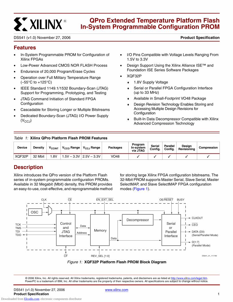
DescriptionXilinx introduces the QPro version of the Platform Flash series of in-system programmable configuration PROMs. Available in 32 Megabit (Mbit) density, this PROM provides an easy-to-use, cost-effective, and reprogrammable method
for storing large Xilinx FPGA configuration bitstreams. The 32-Mbit PROM supports Master Serial, Slave Serial, Master SelectMAP, and Slave SelectMAP FPGA configuration modes (Figure 1).
<BLB
QPro Extended Temperature Platform FlashIn-System Programmable Configuration PROM
DS541 (v1.0) November 27, 2006 0 Product Specification
R
Table 1: Xilinx QPro Platform Flash PROM Features
Device Density VCCINT VCCO Range VCCJ Range PackagesProgram
In-systemvia JTAG
Serial Config.
Parallel Config.
Design Revisioning Compression
XQF32P 32 Mbit 1.8V 1.5V – 3.3V 2.5V – 3.3V VO48 ✓ ✓ ✓ ✓ ✓
Figure 1: XQF32P Platform Flash PROM Block Diagram
CLKOUT
CEO
DATA (D0)(Serial/Parallel Mode)
D[1:7](Parallel Mode)
TCKTMSTDITDO
CLK CE EN_EXT_SEL OE/RESET BUSY
Data
Data
Address
REV_SEL [1:0]CF
Controland
JTAGInterface
Memory
OSC
Serialor
ParallelInterface
Decompressor
DS541_01_111706
Downloaded from Elcodis.com electronic components distributor
QPro Extended Temperature Platform Flash In-System Programmable Configuration PROM
DS541 (v1.0) November 27, 2006 www.xilinx.comProduct Specification 2
R
When the FPGA is in Master Serial mode, it generates a configuration clock that drives the PROM. With CF High, a short access time after CE and OE are enabled, data is available on the PROM DATA (D0) pin that is connected to the FPGA DIN pin. New data is available a short access time after each rising clock edge. The FPGA generates the appropriate number of clock pulses to complete the configuration.
When the FPGA is in Slave Serial mode, the PROM and the FPGA are both clocked by an external clock source, or optionally, the PROM can be used to drive the FPGA’s configuration clock.
The XQF32P QPro version of the Platform Flash PROM also supports Master SelectMAP and Slave SelectMAP (or Slave Parallel) FPGA configuration modes. When the FPGA is in Master SelectMAP mode, the FPGA generates a configuration clock that drives the PROM. When the FPGA is in Slave SelectMAP Mode, either an external oscillator generates the configuration clock that drives the PROM and the FPGA, or optionally, the XQF32P PROM can be used to drive the FPGA’s configuration clock. With BUSY Low and CF High, after CE and OE are enabled, data is available on the PROM DATA (D0-D7) pins. New data is available a short access time after each rising clock edge. The data is clocked into the FPGA on the following rising edge of the CCLK. A free-running oscillator can be used in the Slave Parallel /Slave SelecMAP mode.
The XQF32P QPro version of the Platform Flash PROM provides additional advanced features. A built-in data decompressor supports utilizing compressed PROM files, and design revisioning allows multiple design revisions to be stored on a single PROM or stored across several PROMs. For design revisioning, external pins or internal control bits are used to select the active design revision.
Multiple Platform Flash PROM devices can be cascaded to support the larger configuration files required when targeting larger FPGA devices or targeting multiple FPGAs daisy chained together. When utilizing the advanced features for the XQF32P Platform Flash PROM, such as design revisioning, programming files which span cascaded PROM devices can only be created for cascaded chains containing only XQF32P PROMs.
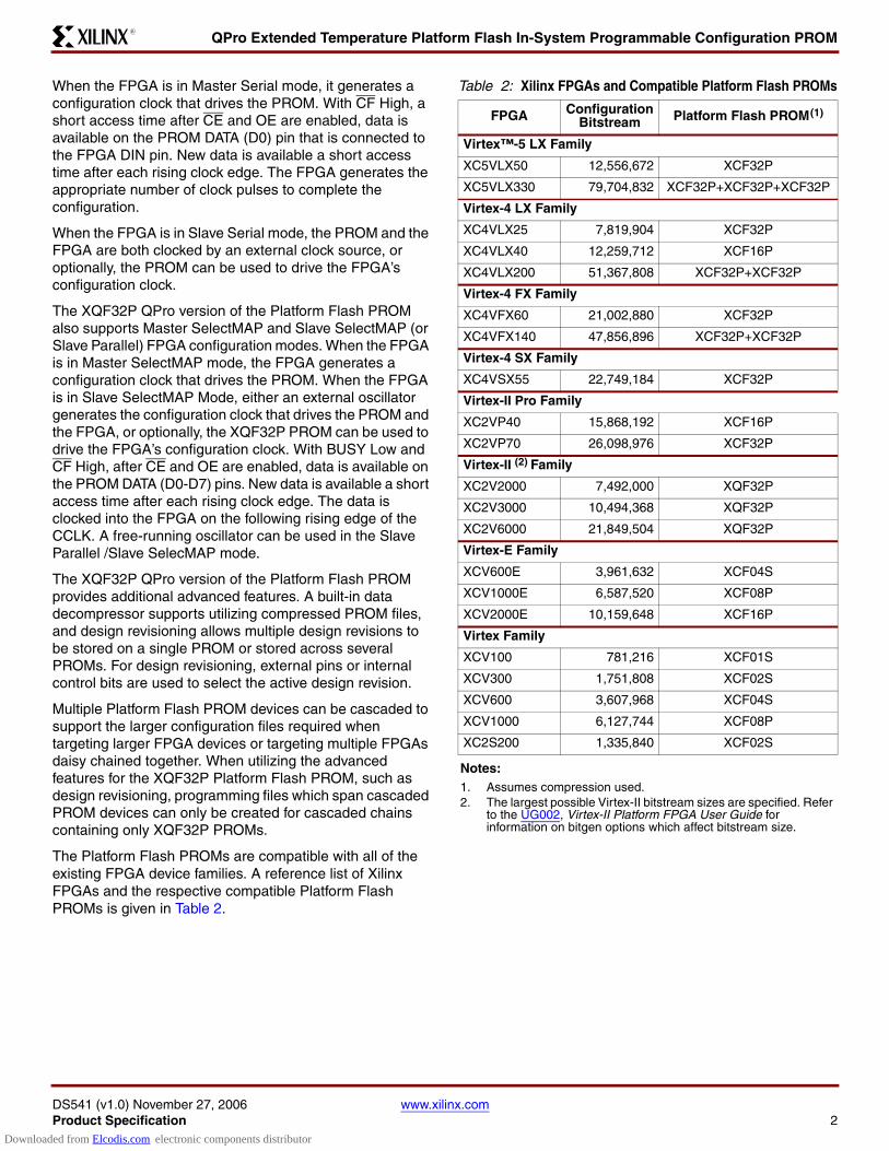
The Platform Flash PROMs are compatible with all of the existing FPGA device families. A reference list of Xilinx FPGAs and the respective compatible Platform Flash PROMs is given in Table 2.
Table 2: Xilinx FPGAs and Compatible Platform Flash PROMs
FPGA Configuration Bitstream Platform Flash PROM(1)
Virtex™-5 LX Family
XC5VLX50 12,556,672 XCF32P
XC5VLX330 79,704,832 XCF32P+XCF32P+XCF32P
Virtex-4 LX Family
XC4VLX25 7,819,904 XCF32P
XC4VLX40 12,259,712 XCF16P
XC4VLX200 51,367,808 XCF32P+XCF32P
Virtex-4 FX Family
XC4VFX60 21,002,880 XCF32P
XC4VFX140 47,856,896 XCF32P+XCF32P
Virtex-4 SX Family
XC4VSX55 22,749,184 XCF32P
Virtex-II Pro Family
XC2VP40 15,868,192 XCF16P
XC2VP70 26,098,976 XCF32P
Virtex-II (2) Family
XC2V2000 7,492,000 XQF32P
XC2V3000 10,494,368 XQF32P
XC2V6000 21,849,504 XQF32P
Virtex-E Family
XCV600E 3,961,632 XCF04S
XCV1000E 6,587,520 XCF08P
XCV2000E 10,159,648 XCF16P
Virtex Family
XCV100 781,216 XCF01S
XCV300 1,751,808 XCF02S
XCV600 3,607,968 XCF04S
XCV1000 6,127,744 XCF08P
XC2S200 1,335,840 XCF02S
Notes: 1. Assumes compression used.2. The largest possible Virtex-II bitstream sizes are specified. Refer
to the UG002, Virtex-II Platform FPGA User Guide for information on bitgen options which affect bitstream size.
Downloaded from Elcodis.com electronic components distributor
QPro Extended Temperature Platform Flash In-System Programmable Configuration PROM
DS541 (v1.0) November 27, 2006 www.xilinx.comProduct Specification 3
R
Programming
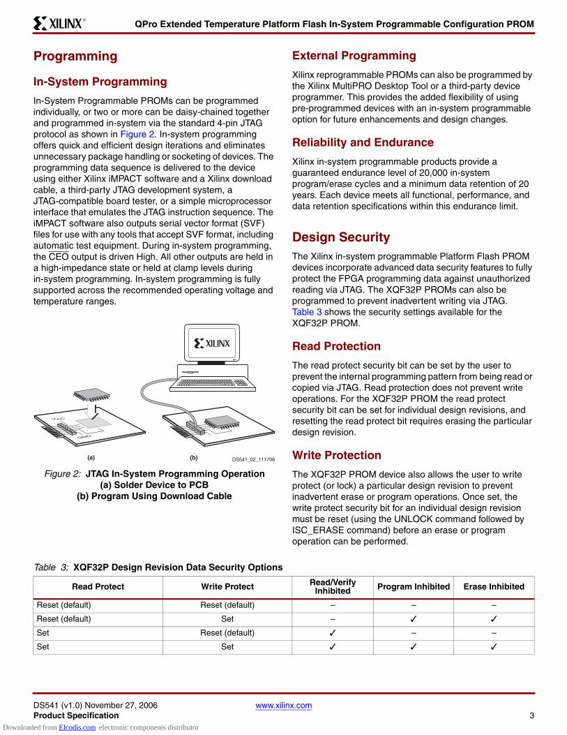
In-System Programming
In-System Programmable PROMs can be programmed individually, or two or more can be daisy-chained together and programmed in-system via the standard 4-pin JTAG protocol as shown in Figure 2. In-system programming offers quick and efficient design iterations and eliminates unnecessary package handling or socketing of devices. The programming data sequence is delivered to the device using either Xilinx iMPACT software and a Xilinx download cable, a third-party JTAG development system, a JTAG-compatible board tester, or a simple microprocessor interface that emulates the JTAG instruction sequence. The iMPACT software also outputs serial vector format (SVF) files for use with any tools that accept SVF format, including automatic test equipment. During in-system programming, the CEO output is driven High. All other outputs are held in a high-impedance state or held at clamp levels during in-system programming. In-system programming is fully supported across the recommended operating voltage and temperature ranges.
External Programming
Xilinx reprogrammable PROMs can also be programmed by the Xilinx MultiPRO Desktop Tool or a third-party device programmer. This provides the added flexibility of using pre-programmed devices with an in-system programmable option for future enhancements and design changes.
Reliability and Endurance
Xilinx in-system programmable products provide a guaranteed endurance level of 20,000 in-system program/erase cycles and a minimum data retention of 20 years. Each device meets all functional, performance, and data retention specifications within this endurance limit.
Design SecurityThe Xilinx in-system programmable Platform Flash PROM devices incorporate advanced data security features to fully protect the FPGA programming data against unauthorized reading via JTAG. The XQF32P PROMs can also be programmed to prevent inadvertent writing via JTAG. Table 3 shows the security settings available for the XQF32P PROM.
Read Protection
The read protect security bit can be set by the user to prevent the internal programming pattern from being read or copied via JTAG. Read protection does not prevent write operations. For the XQF32P PROM the read protect security bit can be set for individual design revisions, and resetting the read protect bit requires erasing the particular design revision.
Write Protection
The XQF32P PROM device also allows the user to write protect (or lock) a particular design revision to prevent inadvertent erase or program operations. Once set, the write protect security bit for an individual design revision must be reset (using the UNLOCK command followed by ISC_ERASE command) before an erase or program operation can be performed.
Figure 2: JTAG In-System Programming Operation (a) Solder Device to PCB
(b) Program Using Download Cable
DS541_02_111706
GND
V CC
(a) (b)
Table 3: XQF32P Design Revision Data Security Options
Read Protect Write Protect Read/Verify Inhibited Program Inhibited Erase Inhibited
Reset (default) Reset (default) – – –
Reset (default) Set – ✓ ✓
Set Reset (default) ✓ – –
Set Set ✓ ✓ ✓
Downloaded from Elcodis.com electronic components distributor
QPro Extended Temperature Platform Flash In-System Programmable Configuration PROM
DS541 (v1.0) November 27, 2006 www.xilinx.comProduct Specification 4
R
IEEE 1149.1 Boundary-Scan (JTAG)The Platform Flash PROM family is compatible with the IEEE 1149.1 boundary-scan standard and the IEEE 1532 in-system configuration standard. A Test Access Port (TAP) and registers are provided to support all required boundary scan instructions, as well as many of the optional instructions specified by IEEE Std. 1149.1. In addition, the JTAG interface is used to implement in-system programming (ISP) to facilitate configuration, erasure, and verification operations on the Platform Flash PROM device. Table 4, page 4 lists the required and optional boundary-scan instructions supported in the Platform Flash PROMs. Refer to the IEEE Std. 1149.1 specification for a complete description of boundary-scan architecture and the required and optional instructions.
Caution! The XQF32P JTAG TAP pause states are not fully compliant with the JTAG 1149.1 specification. If a temporary pause of a JTAG shift operation is required, then stop the JTAG TCK clock and maintain the JTAG TAP within the JTAG Shift-IR or Shift-DR TAP state. Do not transition the XQF32P JTAG TAP through the JTAG Pause-IR or Pause-DR TAP state to temporarily pause a JTAG shift operation.
Instruction Register
The Instruction Register (IR) for the Platform Flash PROM is connected between TDI and TDO during an instruction scan sequence. In preparation for an instruction scan sequence, the instruction register is parallel loaded with a fixed instruction capture pattern. This pattern is shifted out
onto TDO (LSB first), while an instruction is shifted into the instruction register from TDI.
XQF32P Instruction Register (16 bits wide)
The Instruction Register (IR) for the XQF32P PROM is sixteen bits wide and is connected between TDI and TDO during an instruction scan sequence. The detailed composition of the instruction capture pattern is illustrated in Table 5, page 5.
The instruction capture pattern shifted out of the XQF32P device includes IR[15:0]. IR[15:9] are reserved bits and are set to a logic 0. The ISC Error field, IR[8:7], contains a 10 when an ISC operation is a success; otherwise a 01 when an In-System Configuration (ISC) operation fails. The Erase/Program (ER/PROG) Error field, IR[6:5], contains a 10 when an erase or program operation is a success; otherwise a 01 when an erase or program operation fails. The Erase/Program (ER/PROG) Status field, IR[4], contains a logic 0 when the device is busy performing an erase or programming operation; otherwise, it contains a logic 1. The ISC Status field, IR[3], contains logic 1 if the device is currently in In-System Configuration (ISC) mode; otherwise, it contains logic 0. The DONE field, IR[2], contains logic 1 if the sampled design revision has been successfully programmed; otherwise, a logic 0 indicates incomplete programming. The remaining bits IR[1:0] are set to 01 as defined by IEEE Std. 1149.1.
Table 4: Platform Flash PROM Boundary Scan Instructions
Boundary-Scan Command XQF32P IR[15:0] (hex) Instruction Description
Required Instructions
BYPASS FFFF Enables BYPASS.
SAMPLE/PRELOAD 0001 Enables boundary-scan SAMPLE/PRELOAD operation.
EXTEST 0000 Enables boundary-scan EXTEST operation.
Optional Instructions
CLAMP 00FA Enables boundary-scan CLAMP operation.
HIGHZ 00FC Places all outputs in high-impedance state simultaneously.
IDCODE 00FE Enables shifting out 32-bit IDCODE.
USERCODE 00FD Enables shifting out 32-bit USERCODE.
Platform Flash PROM Specific Instructions
CONFIG 00EE Initiates FPGA configuration by pulsing CF pin Low once (for the XQF32P, this command also resets the selected design revision based on either the external REV_SEL[1:0] pins or on the internal design revision selection bits).(1)
Notes: 1. For more information see "Initiating FPGA Configuration," page 11.
Downloaded from Elcodis.com electronic components distributor
QPro Extended Temperature Platform Flash In-System Programmable Configuration PROM
DS541 (v1.0) November 27, 2006 www.xilinx.comProduct Specification 5
R
Boundary Scan Register
The boundary-scan register is used to control and observe the state of the device pins during the EXTEST, SAMPLE/PRELOAD, and CLAMP instructions. Each output pin on the Platform Flash PROM has two register stages which contribute to the boundary-scan register, while each input pin has only one register stage. The bidirectional pins have a total of three register stages which contribute to the boundary-scan register. For each output pin, the register stage nearest to TDI controls and observes the output state, and the second stage closest to TDO controls and observes the High-Z enable state of the output pin. For each input pin, a single register stage controls and observes the input state of the pin. The bidirectional pin combines the three bits, the input stage bit is first, followed by the output stage bit and finally the output enable stage bit. The output enable stage bit is closest to TDO.
See the XQF32P Pin Names and Descriptions Tables in the "Pinouts and Pin Descriptions," page 33 section for the boundary-scan bit order for all connected device pins, or see the appropriate BSDL file for the complete boundary-scan bit order description under the "attribute BOUNDARY_REGISTER" section in the BSDL file. The bit assigned to boundary-scan cell 0 is the LSB in the boundary-scan register, and is the register bit closest to TDO.
Identification Registers
IDCODE Register
The IDCODE is a fixed, vendor-assigned value that is used to electrically identify the manufacturer and type of the device being addressed. The IDCODE register is 32 bits wide. The IDCODE register can be shifted out for examination by using the IDCODE instruction. The IDCODE is available to any other system component via JTAG.
The IDCODE register has the following binary format:
vvvv:ffff:ffff:aaaa:aaaa:cccc:cccc:ccc1
where
v = the die version numberf = the PROM family codea = the specific Platform Flash PROM product IDc = the Xilinx manufacturer's ID
The LSB of the IDCODE register is always read as logic 1 as defined by IEEE Std. 1149.1. The IDCODE register value for the XQ32PPlatform Flash PROM is <v>5059093.
Note: The <v> in the IDCODE field represents the device’s revision code (in hex) and can vary.
USERCODE Register
The USERCODE instruction gives access to a 32-bit user programmable scratch pad typically used to supply information about the device's programmed contents. By using the USERCODE instruction, a user-programmable identification code can be shifted out for examination. This code is loaded into the USERCODE register during programming of the Platform Flash PROM. If the device is blank or was not loaded during programming, the USERCODE register contains FFFFFFFFh.
Customer Code Register
For the XQF32P Platform Flash PROM, in addition to the USERCODE, a unique 32-byte Customer Code can be assigned to each design revision enabled for the PROM. The Customer Code is set during programming, and is typically used to supply information about the design revision contents. A private JTAG instruction is required to read the Customer Code. If the PROM is blank, or the Customer Code for the selected design revision was not loaded during programming, or if the particular design revision is erased, the Customer Code contains all ones.
Platform Flash PROM TAP CharacteristicsThe Platform Flash PROM family performs both in-system programming and IEEE 1149.1 boundary-scan (JTAG) testing via a single 4-wire Test Access Port (TAP). This simplifies system designs and allows standard Automatic Test Equipment to perform both functions. The AC characteristics of the Platform Flash PROM TAP are described as follows.
TAP Timing
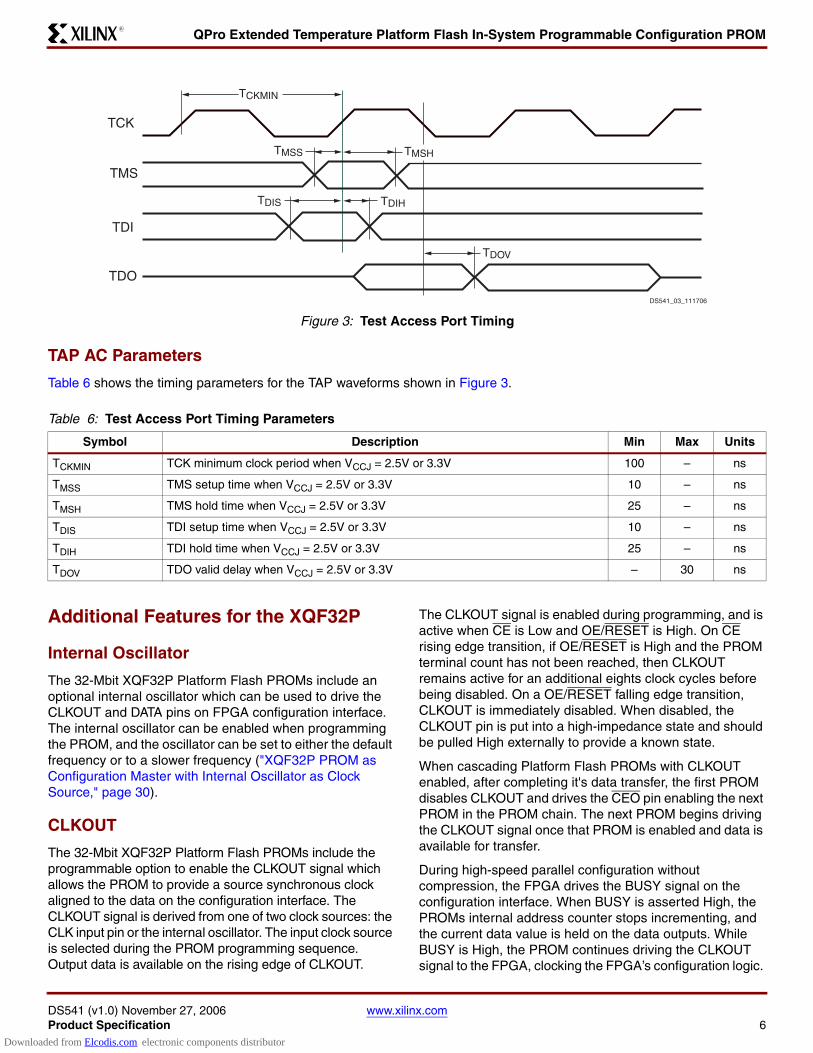
Figure 3, page 6 shows the timing relationships of the TAP signals. These TAP timing characteristics are identical for both boundary-scan and ISP operations.
Table 5: XQF32P Instruction Capture Values Loaded into IR as part of an Instruction Scan Sequence
TDI → IR[15:9] IR[8:7] IR[6:5] IR[4] IR[3] IR[2] IR[1:0]
→ TDOReserved ISC Error ER/PROG
ErrorER/PROG
Status ISC Status DONE 0 1
Downloaded from Elcodis.com electronic components distributor
QPro Extended Temperature Platform Flash In-System Programmable Configuration PROM
DS541 (v1.0) November 27, 2006 www.xilinx.comProduct Specification 6
R
TAP AC Parameters
Table 6 shows the timing parameters for the TAP waveforms shown in Figure 3.
Additional Features for the XQF32P
Internal Oscillator
The 32-Mbit XQF32P Platform Flash PROMs include an optional internal oscillator which can be used to drive the CLKOUT and DATA pins on FPGA configuration interface. The internal oscillator can be enabled when programming the PROM, and the oscillator can be set to either the default frequency or to a slower frequency ("XQF32P PROM as Configuration Master with Internal Oscillator as Clock Source," page 30).
CLKOUT
The 32-Mbit XQF32P Platform Flash PROMs include the programmable option to enable the CLKOUT signal which allows the PROM to provide a source synchronous clock aligned to the data on the configuration interface. The CLKOUT signal is derived from one of two clock sources: the CLK input pin or the internal oscillator. The input clock source is selected during the PROM programming sequence. Output data is available on the rising edge of CLKOUT.
The CLKOUT signal is enabled during programming, and is active when CE is Low and OE/RESET is High. On CE rising edge transition, if OE/RESET is High and the PROM terminal count has not been reached, then CLKOUT remains active for an additional eights clock cycles before being disabled. On a OE/RESET falling edge transition, CLKOUT is immediately disabled. When disabled, the CLKOUT pin is put into a high-impedance state and should be pulled High externally to provide a known state.
When cascading Platform Flash PROMs with CLKOUT enabled, after completing it's data transfer, the first PROM disables CLKOUT and drives the CEO pin enabling the next PROM in the PROM chain. The next PROM begins driving the CLKOUT signal once that PROM is enabled and data is available for transfer.
During high-speed parallel configuration without compression, the FPGA drives the BUSY signal on the configuration interface. When BUSY is asserted High, the PROMs internal address counter stops incrementing, and the current data value is held on the data outputs. While BUSY is High, the PROM continues driving the CLKOUT signal to the FPGA, clocking the FPGA’s configuration logic.
Figure 3: Test Access Port Timing
TCK
TCKMIN
TMSS
TMS
TDI
TDO
TMSH
TDIH
TDOV
TDIS
DS541_03_111706
Table 6: Test Access Port Timing Parameters
Symbol Description Min Max Units
TCKMIN TCK minimum clock period when VCCJ = 2.5V or 3.3V 100 – ns
TMSS TMS setup time when VCCJ = 2.5V or 3.3V 10 – ns
TMSH TMS hold time when VCCJ = 2.5V or 3.3V 25 – ns
TDIS TDI setup time when VCCJ = 2.5V or 3.3V 10 – ns
TDIH TDI hold time when VCCJ = 2.5V or 3.3V 25 – ns
TDOV TDO valid delay when VCCJ = 2.5V or 3.3V – 30 ns
Downloaded from Elcodis.com electronic components distributor
QPro Extended Temperature Platform Flash In-System Programmable Configuration PROM
DS541 (v1.0) November 27, 2006 www.xilinx.comProduct Specification 7
R
When the FPGA deasserts BUSY, indicating that it is ready to receive additional configuration data, the PROM begins driving new data onto the configuration interface.
Decompression
The 32-Mbit XQF32P Platform Flash PROMs include a built-in data decompressor compatible with Xilinx advanced compression technology. Compressed Platform Flash PROM files are created from the target FPGA bitstream(s) using the iMPACT software. Only Slave Serial and Slave SelectMAP (parallel) configuration modes are supported for FPGA configuration when using a XQF32P PROM programmed with a compressed bitstream. Compression rates vary depending on several factors, including the target device family and the target design contents.
The decompression option is enabled during the PROM programming sequence. The PROM decompresses the stored data before driving both clock and data onto the FPGA's configuration interface. If Decompression is enabled, then the Platform Flash clock output pin (CLKOUT) must be used as the clock signal for the configuration interface, driving the target FPGA's configuration clock input pin (CCLK). Either the PROM's CLK input pin or the internal oscillator must be selected as the source for CLKOUT. Any target FPGA connected to the PROM must operate as slave in the configuration chain, with the configuration mode set to Slave Serial mode or Slave SelectMap (parallel) mode.
When decompression is enabled, the CLKOUT signal becomes a controlled clock output with a reduced maximum frequency. When decompressed data is not ready, the CLKOUT pin is put into a high-Z state and must be pulled High externally to provide a known state.
The BUSY input is automatically disabled when decompression is enabled.
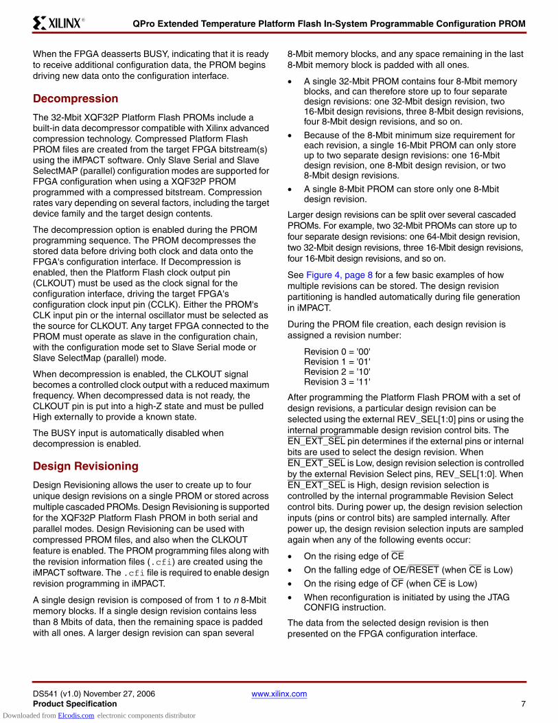
Design Revisioning
Design Revisioning allows the user to create up to four unique design revisions on a single PROM or stored across multiple cascaded PROMs. Design Revisioning is supported for the XQF32P Platform Flash PROM in both serial and parallel modes. Design Revisioning can be used with compressed PROM files, and also when the CLKOUT feature is enabled. The PROM programming files along with the revision information files (.cfi) are created using the iMPACT software. The .cfi file is required to enable design revision programming in iMPACT.
A single design revision is composed of from 1 to n 8-Mbit memory blocks. If a single design revision contains less than 8 Mbits of data, then the remaining space is padded with all ones. A larger design revision can span several
8-Mbit memory blocks, and any space remaining in the last 8-Mbit memory block is padded with all ones.
• A single 32-Mbit PROM contains four 8-Mbit memory blocks, and can therefore store up to four separate design revisions: one 32-Mbit design revision, two 16-Mbit design revisions, three 8-Mbit design revisions, four 8-Mbit design revisions, and so on.
• Because of the 8-Mbit minimum size requirement for each revision, a single 16-Mbit PROM can only store up to two separate design revisions: one 16-Mbit design revision, one 8-Mbit design revision, or two 8-Mbit design revisions.
• A single 8-Mbit PROM can store only one 8-Mbit design revision.
Larger design revisions can be split over several cascaded PROMs. For example, two 32-Mbit PROMs can store up to four separate design revisions: one 64-Mbit design revision, two 32-Mbit design revisions, three 16-Mbit design revisions, four 16-Mbit design revisions, and so on.
See Figure 4, page 8 for a few basic examples of how multiple revisions can be stored. The design revision partitioning is handled automatically during file generation in iMPACT.
During the PROM file creation, each design revision is assigned a revision number:
Revision 0 = '00' Revision 1 = '01'Revision 2 = '10'Revision 3 = '11'
After programming the Platform Flash PROM with a set of design revisions, a particular design revision can be selected using the external REV_SEL[1:0] pins or using the internal programmable design revision control bits. The EN_EXT_SEL pin determines if the external pins or internal bits are used to select the design revision. When EN_EXT_SEL is Low, design revision selection is controlled by the external Revision Select pins, REV_SEL[1:0]. When EN_EXT_SEL is High, design revision selection is controlled by the internal programmable Revision Select control bits. During power up, the design revision selection inputs (pins or control bits) are sampled internally. After power up, the design revision selection inputs are sampled again when any of the following events occur:
• On the rising edge of CE
• On the falling edge of OE/RESET (when CE is Low)
• On the rising edge of CF (when CE is Low)
• When reconfiguration is initiated by using the JTAG CONFIG instruction.
The data from the selected design revision is then presented on the FPGA configuration interface.
Downloaded from Elcodis.com electronic components distributor
QPro Extended Temperature Platform Flash In-System Programmable Configuration PROM
DS541 (v1.0) November 27, 2006 www.xilinx.comProduct Specification 8
R
PROM to FPGA Configuration Mode and Connections SummaryThe FPGA's I/O, logical functions, and internal interconnections are established by the configuration data contained in the FPGA’s bitstream. The bitstream is loaded into the FPGA either automatically upon power up, or on command, depending on the state of the FPGA's mode pins. Xilinx Platform Flash PROMs are designed to download directly to the FPGA configuration interface. FPGA configuration modes which are supported by the XQF32P Platform Flash PROMs include: Master Serial, Slave Serial, Master SelectMAP, and Slave SelectMAP. Below is a short summary of the supported FPGA configuration modes. See the respective FPGA data sheet for device configuration details, including which configuration modes are supported by the targeted FPGA device.
FPGA Master Serial Mode
In Master Serial mode, the FPGA automatically loads the configuration bitstream in bit-serial form from external memory synchronized by the configuration clock (CCLK) generated by the FPGA. Upon power-up or reconfiguration, the FPGA's mode select pins are used to select the Master Serial configuration mode. Master Serial Mode provides a simple configuration interface. Only a serial data line, a clock line, and two control lines (INIT and DONE) are required to configure an FPGA. Data from the PROM is read out sequentially on a single data line (DIN), accessed via the PROM's internal address counter which is incremented on every valid rising edge of CCLK. The serial bitstream data must be set up at the FPGA’s DIN input pin a short time before each rising edge of the FPGA's internally generated CCLK signal.
Figure 4: Design Revision Storage Examples
REV 0(8 Mbits)
REV 1(8 Mbits)
REV 2(8 Mbits)
REV 3(8 Mbits)
REV 0(8 Mbits)
REV 1(8 Mbits)
REV 2(16 Mbits)
REV 0(16 Mbits)
REV 1(16 Mbits)
REV 0(8 Mbits)
REV 1(24 Mbits)
REV 0(32 Mbits)
4 Design Revisions 3 Design Revisions 2 Design Revisions 1 Design Revision
(a) Design Revision storage examples for a single XQF32P PROM
REV 0(16 Mbits)
REV 1(16 Mbits)
REV 2(16 Mbits)
REV 3(16 Mbits)
REV 0(16 Mbits)
REV 1(16 Mbits)
REV 2(32 Mbits)
REV 0(32 Mbits)
REV 1(32 Mbits)
REV 0(16 Mbits)
REV 1(16 Mbits)
REV 0(32 Mbits)
4 Design Revisions 3 Design Revisions 2 Design Revisions 1 Design Revision
(b) Design Revision storage examples spanning two XQF32P PROMs
PROM 0 PROM 0 PROM 0 PROM 0 PROM 0
PROM 0 PROM 0 PROM 0 PROM 0 PROM 0
REV 0(32 Mbits)
REV 1(32 Mbits)
PROM 1 PROM 1 PROM 1 PROM 1 PROM 1
ds541_04_070906
Downloaded from Elcodis.com electronic components distributor

QPro Extended Temperature Platform Flash In-System Programmable Configuration PROM
DS541 (v1.0) November 27, 2006 www.xilinx.comProduct Specification 9
R
Typically, a wide range of frequencies can be selected for the FPGA’s internally generated CCLK which always starts at a slow default frequency. The FPGA’s bitstream contains configuration bits which can switch CCLK to a higher frequency for the remainder of the Master Serial configuration sequence. The desired CCLK frequency is selected during bitstream generation.
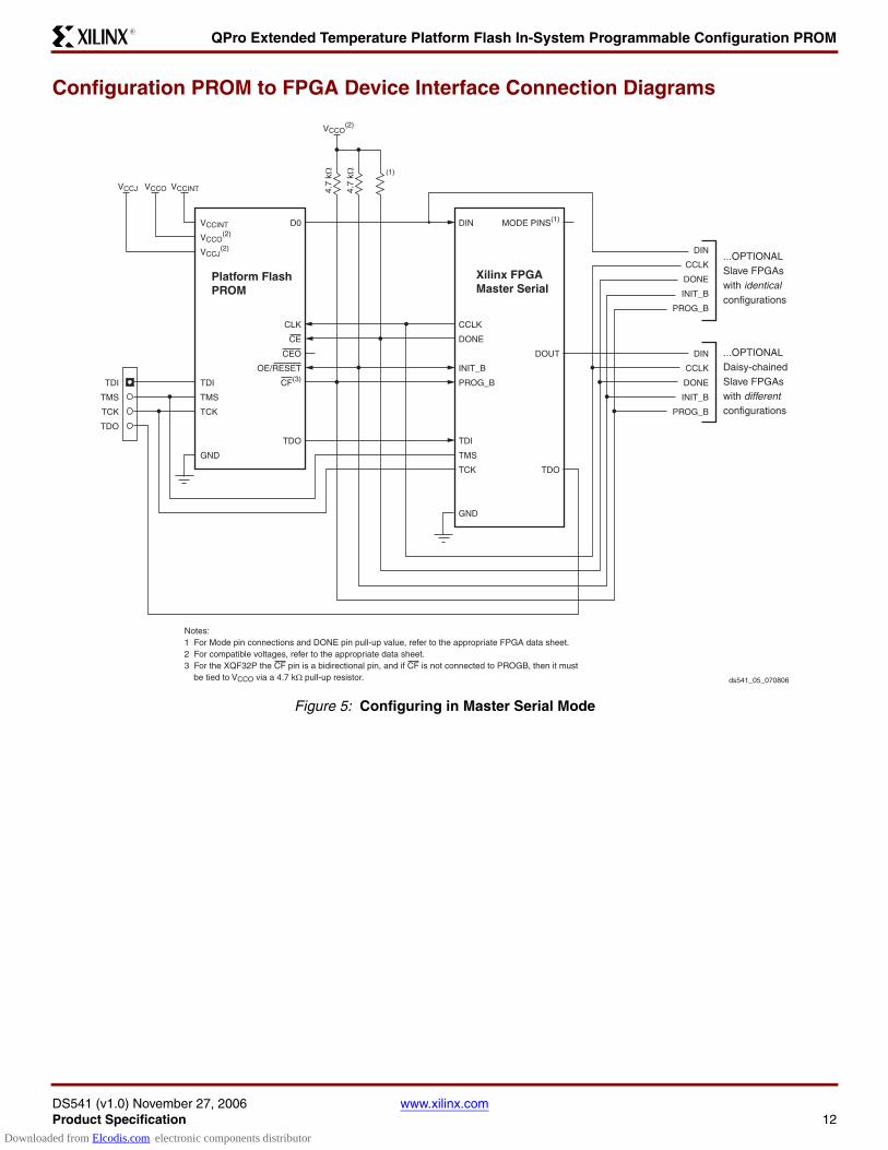
Connecting the FPGA device to the configuration PROM for Master Serial Configuration Mode (Figure 5, page 12):
• The DATA output of the PROM(s) drive the DIN input of the lead FPGA device.
• The Master FPGA CCLK output drives the CLK input(s) of the PROM(s)
• The CEO output of a PROM drives the CE input of the next PROM in a daisy chain (if any).
• The OE/RESET pins of all PROMs are connected to the INIT_B pins of all FPGA devices. This connection assures that the PROM address counter is reset before the start of any (re)configuration.
• The PROM CE input can be driven from the DONE pin. The CE input of the first (or only) PROM can be driven by the DONE output of all target FPGA devices, provided that DONE is not permanently grounded. CE can also be permanently tied Low, but this keeps the DATA output active and causes an unnecessary ICC active supply current ("DC Characteristics Over Operating Conditions," page 24).
• The PROM CF pin is typically connected to the FPGA's PROG_B (or PROGRAM) input. For the XQF32P only, the CF pin is a bidirectional pin. If the XQF32P CF pin is not connected to the FPGA's PROG_B (or PROGRAM) input, then the pin should be tied High.
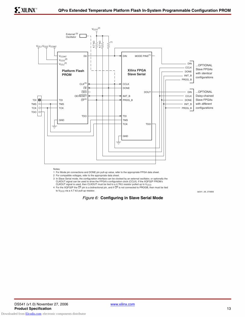
FPGA Slave Serial Mode
In Slave Serial mode, the FPGA loads the configuration bitstream in bit-serial form from external memory synchronized by an externally supplied clock. Upon power-up or reconfiguration, the FPGA's mode select pins are used to select the Slave Serial configuration mode. Slave Serial Mode provides a simple configuration interface. Only a serial data line, a clock line, and two control lines (INIT and DONE) are required to configure an FPGA. Data from the PROM is read out sequentially on a single data line (DIN), accessed via the PROM's internal address counter which is incremented on every valid rising edge of CCLK. The serial bitstream data must be set up at the FPGA’s DIN input pin a short time before each rising edge of the externally provided CCLK.
Connecting the FPGA device to the configuration PROM for Slave Serial Configuration Mode (Figure 6, page 13):
• The DATA output of the PROM(s) drive the DIN input of the lead FPGA device.
• The PROM CLKOUT (for XQF32P only) or an external clock source drives the FPGA's CCLK input.
• The CEO output of a PROM drives the CE input of the next PROM in a daisy chain (if any).
• The OE/RESET pins of all PROMs are connected to the INIT_B (or INIT) pins of all FPGA devices. This connection assures that the PROM address counter is reset before the start of any (re)configuration.
• The PROM CE input can be driven from the DONE pin. The CE input of the first (or only) PROM can be driven by the DONE output of all target FPGA devices, provided that DONE is not permanently grounded. CE can also be permanently tied Low, but this keeps the DATA output active and causes an unnecessary ICC active supply current ("DC Characteristics Over Operating Conditions," page 24).
• The PROM CF pin is typically connected to the FPGA's PROG_B (or PROGRAM) input. For the XQF32P only, the CF pin is a bidirectional pin. If the XQF32P CF pin is not connected to the FPGA's PROG_B (or PROGRAM) input, then the pin should be tied High.
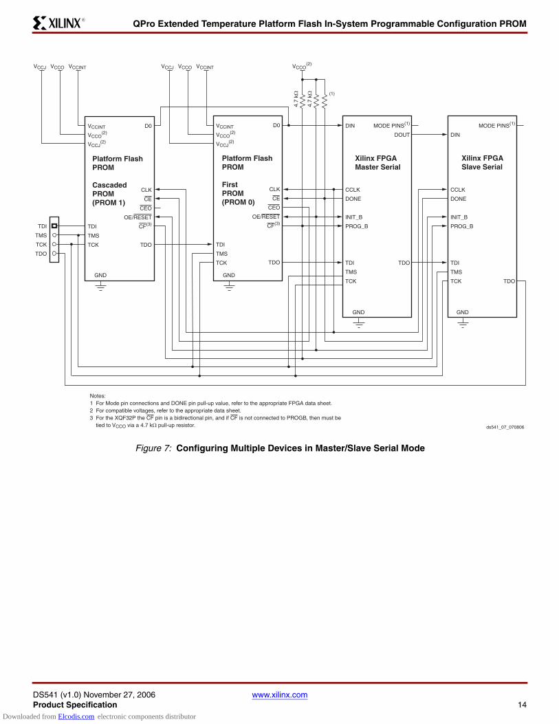
Serial Daisy Chain
Multiple FPGAs can be daisy-chained for serial configuration from a single source. After a particular FPGA has been configured, the data for the next device is routed internally to the FPGA’s DOUT pin. Typically the data on the DOUT pin changes on the falling edge of CCLK, although for some devices the DOUT pin changes on the rising edge of CCLK. Consult the respective device data sheets for detailed information on a particular FPGA device. For clocking the daisy-chained configuration, either the first FPGA in the chain can be set to Master Serial, generating the CCLK, with the remaining devices set to Slave Serial (Figure 7, page 14), or all the FPGA devices can be set to Slave Serial and an externally generated clock can be used to drive the FPGA's configuration interface (Figure 6, page 13 or Figure 11, page 18).
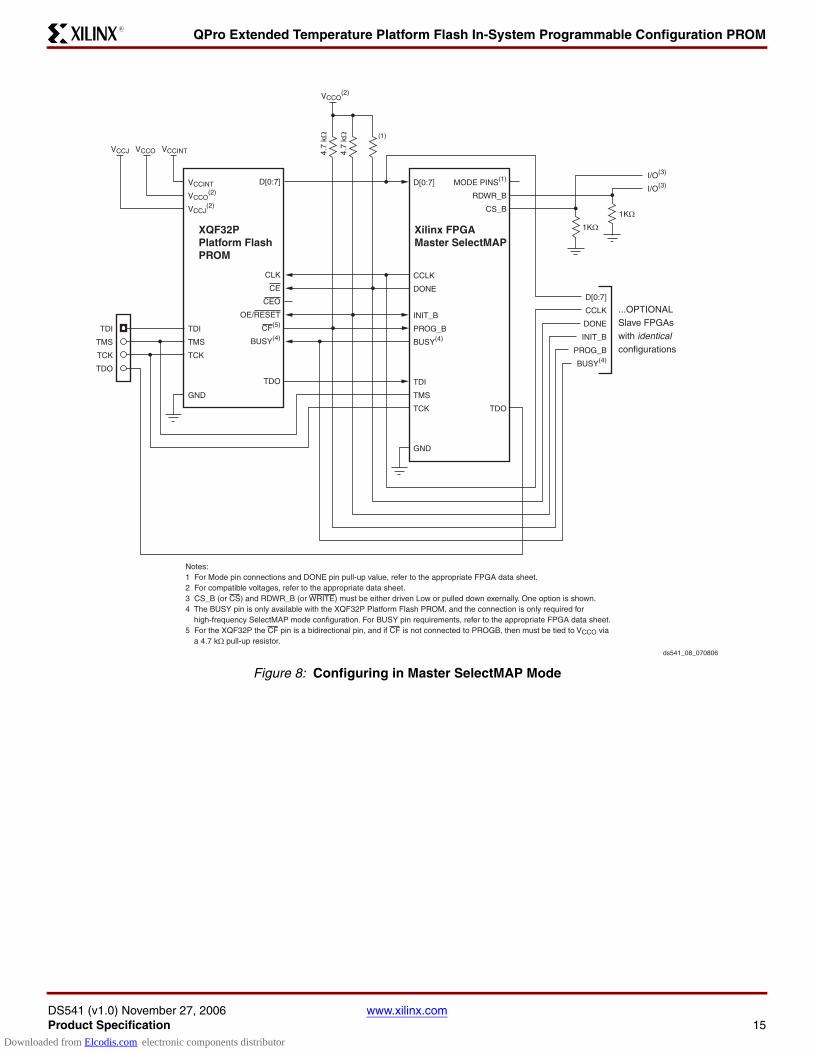
FPGA Master SelectMAP (Parallel) Mode
In Master SelectMAP mode, byte-wide data is written into the FPGA, typically with a BUSY flag controlling the flow of data, synchronized by the configuration clock (CCLK) generated by the FPGA. Upon power-up or reconfiguration, the FPGA's mode select pins are used to select the Master SelectMAP configuration mode. The configuration interface typically requires a parallel data bus, a clock line, and two control lines (INIT and DONE). In addition, the FPGA’s Chip Select, Write, and BUSY pins must be correctly controlled to enable SelectMAP configuration. The configuration data is read from the PROM byte by byte on pins [D0..D7], accessed via the PROM's internal address counter which is incremented on every valid rising edge of CCLK. The bitstream data must be set up at the FPGA’s [D0..D7] input
Downloaded from Elcodis.com electronic components distributor

QPro Extended Temperature Platform Flash In-System Programmable Configuration PROM
DS541 (v1.0) November 27, 2006 www.xilinx.comProduct Specification 10
R
pins a short time before each rising edge of the FPGA's internally generated CCLK signal. If BUSY is asserted (High) by the FPGA, the configuration data must be held until BUSY goes Low. An external data source or external pull-down resistors must be used to enable the FPGA's active Low Chip Select (CS or CS_B) and Write (WRITE or RDWR_B) signals to enable the FPGA's SelectMAP configuration process.
The Master SelectMAP configuration interface is clocked by the FPGA’s internal oscillator. Typically, a wide range of frequencies can be selected for the internally generated CCLK which always starts at a slow default frequency. The FPGA’s bitstream contains configuration bits which can switch CCLK to a higher frequency for the remainder of the Master SelectMAP configuration sequence. The desired CCLK frequency is selected during bitstream generation.
After configuration, the pins of the SelectMAP port can be used as additional user I/O. Alternatively, the port can be retained using the persist option.
Connecting the FPGA device to the configuration PROM for Master SelectMAP (Parallel) Configuration Mode (Figure 8, page 15):
• The DATA outputs of the PROM(s) drive the [D0..D7] input of the lead FPGA device.
• The Master FPGA CCLK output drives the CLK input(s) of the PROM(s)
• The CEO output of a PROM drives the CE input of the next PROM in a daisy chain (if any).
• The OE/RESET pins of all PROMs are connected to the INIT_B pins of all FPGA devices. This connection assures that the PROM address counter is reset before the start of any (re)configuration.
• The PROM CE input can be driven from the DONE pin. The CE input of the first (or only) PROM can be driven by the DONE output of all target FPGA devices, provided that DONE is not permanently grounded. CE can also be permanently tied Low, but this keeps the DATA output active and causes an unnecessary ICC active supply current ("DC Characteristics Over Operating Conditions," page 24).
• For high-frequency parallel configuration, the BUSY pins of all PROMs are connected to the FPGA's BUSY output. This connection assures that the next data transition for the PROM is delayed until the FPGA is ready for the next configuration data byte.
• The PROM CF pin is typically connected to the FPGA's PROG_B (or PROGRAM) input. For the XQF32P only, the CF pin is a bidirectional pin. If the XQF32P CF pin is not connected to the FPGA's PROG_B (or PROGRAM) input, then the pin should be tied High.
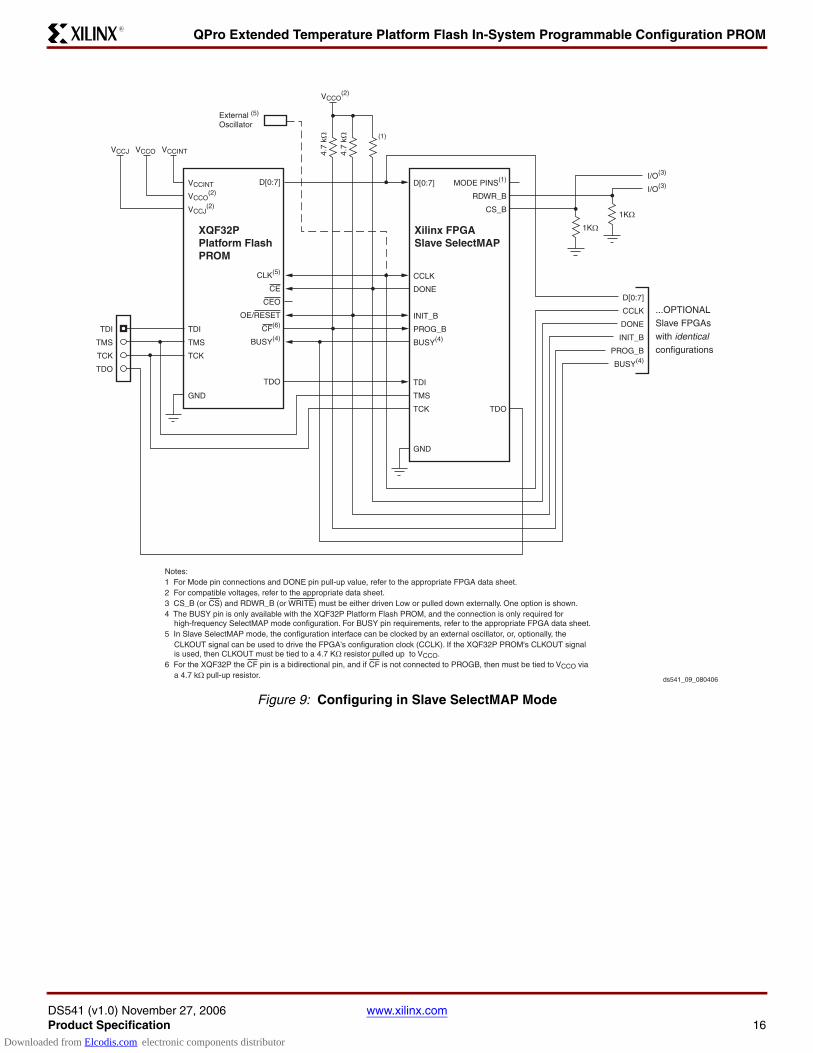
FPGA Slave SelectMAP (Parallel) Mode
In Slave SelectMAP mode, byte-wide data is written into the FPGA, typically with a BUSY flag controlling the flow of data, synchronized by an externally supplied configuration clock (CCLK). Upon power-up or reconfiguration, the FPGA's mode select pins are used to select the Slave SelectMAP configuration mode. The configuration interface typically requires a parallel data bus, a clock line, and two control lines (INIT and DONE). In addition, the FPGA’s Chip Select, Write, and BUSY pins must be correctly controlled to enable SelectMAP configuration. The configuration data is read from the PROM byte by byte on pins [D0..D7], accessed via the PROM's internal address counter which is incremented on every valid rising edge of CCLK. The bitstream data must be set up at the FPGA’s [D0..D7] input pins a short time before each rising edge of the provided CCLK. If BUSY is asserted (High) by the FPGA, the configuration data must be held until BUSY goes Low. An external data source or external pull-down resistors must be used to enable the FPGA's active Low Chip Select (CS or CS_B) and Write (WRITE or RDWR_B) signals to enable the FPGA's SelectMAP configuration process.
After configuration, the pins of the SelectMAP port can be used as additional user I/O. Alternatively, the port can be retained using the persist option.
Connecting the FPGA device to the configuration PROM for Slave SelectMAP (Parallel) Configuration Mode (Figure 9, page 16):
• The DATA outputs of the PROM(s) drives the [D0..D7] inputs of the lead FPGA device.
• The PROM CLKOUT (for XQF32P only) or an external clock source drives the FPGA's CCLK input.
• The CEO output of a PROM drives the CE input of the next PROM in a daisy chain (if any).
• The OE/RESET pins of all PROMs are connected to the INIT_B pins of all FPGA devices. This connection assures that the PROM address counter is reset before the start of any (re)configuration.
• The PROM CE input can be driven from the DONE pin. The CE input of the first (or only) PROM can be driven by the DONE output of all target FPGA devices, provided that DONE is not permanently grounded. CE can also be permanently tied Low, but this keeps the DATA output active and causes an unnecessary ICC active supply current ("DC Characteristics Over Operating Conditions," page 24).
• For high-frequency parallel configuration, the BUSY pins of all PROMs are connected to the FPGA's BUSY output. This connection assures that the next data transition for the PROM is delayed until the FPGA is ready for the next configuration data byte.
Downloaded from Elcodis.com electronic components distributor

QPro Extended Temperature Platform Flash In-System Programmable Configuration PROM
DS541 (v1.0) November 27, 2006 www.xilinx.comProduct Specification 11
R
• The PROM CF pin is typically connected to the FPGA's PROG_B (or PROGRAM) input. For the XQF32P only, the CF pin is a bidirectional pin. If the XQF32P CF pin is not connected to the FPGA's PROG_B (or PROGRAM) input, then the pin should be tied High.
FPGA SelectMAP (Parallel) Device Chaining
Multiple Virtex-II FPGAs can be configured using the SelectMAP mode, and be made to start up simultaneously. To configure multiple devices in this way, wire the individual CCLK, DONE, INIT, Data ([D0..D7]), Write (WRITE or RDWR_B), and BUSY pins of all the devices in parallel. If all devices are to be configured with the same bitstream, readback is not being used, and the CCLK frequency selected does not require the use of the BUSY signal, the CS_B pins can be connected to a common line so all of the devices are configured simultaneously (Figure 9, page 16).
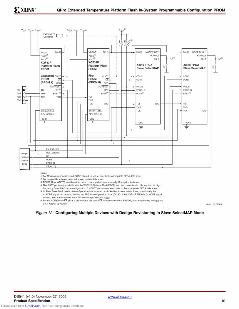
With additional control logic, the individual devices can be loaded separately by asserting the CS_B pin of each device in turn and then enabling the appropriate configuration data. The PROM can also store the individual bitstreams for each FPGA for SelectMAP configuration in separate design revisions. When design revisioning is utilized, additional control logic can be used to select the appropriate bitstream by asserting the EN_EXT_SEL pin, and using the REV_SEL[1:0] pins to select the required bitstream, while asserting the CS_B pin for the FPGA the bitstream is targeting (Figure 12, page 19).
For clocking the parallel configuration chain, either the first FPGA in the chain can be set to Master SelectMAP, generating the CCLK, with the remaining devices set to Slave SelectMAP, or all the FPGA devices can be set to Slave SelectMAP and an externally generated clock can be used to drive the configuration interface. Again, the respective device data sheets should be consulted for detailed information on a particular FPGA device, including which configuration modes are supported by the targeted FPGA device.
Cascading Configuration PROMs
When configuring multiple FPGAs in a serial daisy chain, configuring multiple FPGAs in a SelectMAP parallel chain, or configuring a single FPGA requiring a larger configuration bitstream, cascaded PROMs provide additional memory (Figure 7, page 14, Figure 10, page 17, Figure 11, page 18, and Figure 12, page 19). Multiple Platform Flash PROMs can be concatenated by using the CEO output to drive the CE input of the downstream device. The clock signal and the data outputs of all Platform Flash PROMs in the chain are interconnected. After the last data
from the first PROM is read, the first PROM asserts its CEO output Low and drives its outputs to a high-impedance state. The second PROM recognizes the Low level on its CE input and immediately enables its outputs.
After configuration is complete, address counters of all cascaded PROMs are reset if the PROM OE/RESET pin goes Low or CE goes High.
When utilizing the advanced features for the XQF32P Platform Flash PROM, including the clock output (CLKOUT) option, decompression option, or design revisioning, programming files which span cascaded PROM devices can only be created for cascaded chains containing only XQF32P PROM.
Initiating FPGA Configuration
The options for initiating FPGA configuration via the Platform Flash PROM include:
• Automatic configuration on power up
• Applying an external PROG_B (or PROGRAM) pulse
• Applying the JTAG CONFIG instruction
Following the FPGA’s power-on sequence or the assertion of the PROG_B (or PROGRAM) pin the FPGA’s configuration memory is cleared, the configuration mode is selected, and the FPGA is ready to accept a new configuration bitstream. The FPGA’s PROG_B pin can be controlled by an external source, or alternatively, the Platform Flash PROMs incorporate a CF pin that can be tied to the FPGA’s PROG_B pin. Executing the CONFIG instruction through JTAG pulses the CF output Low once for 300-500 ns, resetting the FPGA and initiating configuration. The iMPACT software can issue the JTAG CONFIG command to initiate FPGA configuration by setting the "Load FPGA" option.
When using the XQF32P Platform Flash PROM with design revisioning enabled, the CF pin should always be connected to the PROG_B (or PROGRAM) pin on the FPGA to ensure that the current design revision selection is sampled when the FPGA is reset. The XQF32P PROM samples the current design revision selection from the external REV_SEL pins or the internal programmable Revision Select bits on the rising edge of CF. When the JTAG CONFIG command is executed, the XQF32P samples the new design revision selection before initiating the FPGA configuration sequence. When using the XQF32P Platform Flash PROM without design revisioning, if the CF pin is not connected to the FPGA PROG_B (or PROGRAM) pin, then the XQF32P CF pin must be tied High.
Downloaded from Elcodis.com electronic components distributor
QPro Extended Temperature Platform Flash In-System Programmable Configuration PROM
DS541 (v1.0) November 27, 2006 www.xilinx.comProduct Specification 12
R
Configuration PROM to FPGA Device Interface Connection Diagrams
Figure 5: Configuring in Master Serial Mode
Notes:1 For Mode pin connections and DONE pin pull-up value, refer to the appropriate FPGA data sheet.2 For compatible voltages, refer to the appropriate data sheet.3 For the XQF32P the CF pin is a bidirectional pin, and if CF is not connected to PROGB, then it must
be tied to VCCO via a 4.7 kΩ pull-up resistor.
Xilinx FPGAMaster Serial
DIN
CCLK
DONE
INIT_B
PROG_B
TDI
TMS
TCK
GND
MODE PINS(1)
DOUT
TDO
VCCJ VCCO VCCINT
DIN
CCLK
DONE
INIT_B
PROG_B
DIN
CCLK
DONE
INIT_B
PROG_B
4.7
kΩ
4.7
kΩ (1)
VCCO(2)
...OPTIONALDaisy-chainedSlave FPGAs with differentconfigurations
...OPTIONALSlave FPGAs with identicalconfigurations
TDI
TMS
TCK
TDO
Platform Flash PROM
VCCINT
VCCO(2)
VCCJ(2)
TDI
TMS
TCK
GND
D0
CLK
CE
CEO
OE/RESET
CF(3)
TDO
ds541_05_070806
Downloaded from Elcodis.com electronic components distributor
QPro Extended Temperature Platform Flash In-System Programmable Configuration PROM
DS541 (v1.0) November 27, 2006 www.xilinx.comProduct Specification 13
R
Figure 6: Configuring in Slave Serial Mode
Notes:1 For Mode pin connections and DONE pin pull-up value, refer to the appropriate FPGA data sheet.2 For compatible voltages, refer to the appropriate data sheet.3 In Slave Serial mode, the configuration interface can be clocked by an external oscillator, or optionally the
CLKOUT signal can be used to drive the FPGA's configuration clock (CCLK). If the XQF32P PROM's CLKOUT signal is used, then CLKOUT must be tied to a 4.7KΩ resistor pulled up to VCCO.
4 For the XQF32P the CF pin is a bidirectional pin, and if CF is not connected to PROGB, then must be tied to VCCO via a 4.7 kΩ pull-up resistor.
Xilinx FPGASlave Serial
DIN
CCLK
DONE
INIT_B
PROG_B
TDI
TMS
TCK
GND
MODE PINS(1)
DOUT
TDO
VCCJ VCCO VCCINT
DIN
CCLK
DONE
INIT_B
PROG_B
DIN
CCLK
DONE
INIT_B
PROG_B
4.7
kΩ
4.7
kΩ (1)
VCCO(2)
...OPTIONALDaisy-chainedSlave FPGAs with differentconfigurations
...OPTIONALSlave FPGAs with identicalconfigurations
TDI
TMS
TCK
TDO
Platform Flash PROM
VCCINT
VCCO(2)
VCCJ(2)
TDI
TMS
TCK
GND
D0
CLK(3)
CE
CEO
OE/RESET
CF(4)
TDO
ds541_06_070806
External (3)
Oscillator
Downloaded from Elcodis.com electronic components distributor
QPro Extended Temperature Platform Flash In-System Programmable Configuration PROM
DS541 (v1.0) November 27, 2006 www.xilinx.comProduct Specification 14
R
Figure 7: Configuring Multiple Devices in Master/Slave Serial Mode
Notes:1 For Mode pin connections and DONE pin pull-up value, refer to the appropriate FPGA data sheet.2 For compatible voltages, refer to the appropriate data sheet.3 For the XQF32P the CF pin is a bidirectional pin, and if CF is not connected to PROGB, then must be
tied to VCCO via a 4.7 kΩ pull-up resistor.
Platform Flash PROM
First PROM(PROM 0)
VCCINT
VCCO(2)
VCCJ(2)
TDI
TMS
TCK
D0
CLK
CE
CEO
OE/RESET
CF(3)
TDO
Xilinx FPGAMaster Serial
DIN
CCLK
DONE
INIT_B
PROG_B
TDI
TMS
TCK
MODE PINS(1)
DOUT
TDO
VCCJ VCCO VCCINT
4.7
kΩ
4.7
kΩ (1)
VCCO(2)
TDI
TMS
TCK
TDO
Xilinx FPGASlave Serial
DIN
CCLK
DONE
INIT_B
PROG_B
TDI
TMS
TCK
Platform Flash PROM
Cascaded PROM(PROM 1)
VCCINT
VCCO(2)
VCCJ(2)
TDI
TMS
TCK
D0
CLK
CE
CEO
OE/RESET
CF(3)
TDO
VCCJ VCCO VCCINT
MODE PINS(1)
TDO
ds541_07_070806
GND
GNDGND
GND
Downloaded from Elcodis.com electronic components distributor
QPro Extended Temperature Platform Flash In-System Programmable Configuration PROM
DS541 (v1.0) November 27, 2006 www.xilinx.comProduct Specification 15
R
Figure 8: Configuring in Master SelectMAP Mode
Notes:1 For Mode pin connections and DONE pin pull-up value, refer to the appropriate FPGA data sheet.2 For compatible voltages, refer to the appropriate data sheet.3 CS_B (or CS) and RDWR_B (or WRITE) must be either driven Low or pulled down exernally. One option is shown.4 The BUSY pin is only available with the XQF32P Platform Flash PROM, and the connection is only required for
high-frequency SelectMAP mode configuration. For BUSY pin requirements, refer to the appropriate FPGA data sheet.5 For the XQF32P the CF pin is a bidirectional pin, and if CF is not connected to PROGB, then must be tied to VCCO via
a 4.7 kΩ pull-up resistor.
XQF32PPlatform Flash PROM
VCCINT
VCCO(2)
VCCJ(2)
TDI
TMS
TCK
GND
D[0:7]
CLK
CE
CEO
OE/RESET
CF(5)
BUSY(4)
TDO
Xilinx FPGAMaster SelectMAP
D[0:7]
CCLK
DONE
INIT_B
PROG_B
BUSY(4)
TDI
TMS
TCK
GND
MODE PINS(1)
RDWR_B
CS_B
TDO
VCCJ VCCO VCCINT
D[0:7]
CCLK
DONE
INIT_B
PROG_B
BUSY(4)
4.7
kΩ
4.7
kΩ (1)
VCCO(2)
...OPTIONALSlave FPGAs with identicalconfigurations
TDI
TMS
TCK
TDO
1KΩ
1KΩ
I/O(3)
I/O(3)
ds541_08_070806
Downloaded from Elcodis.com electronic components distributor
QPro Extended Temperature Platform Flash In-System Programmable Configuration PROM
DS541 (v1.0) November 27, 2006 www.xilinx.comProduct Specification 16
R
Figure 9: Configuring in Slave SelectMAP Mode
Notes:1 For Mode pin connections and DONE pin pull-up value, refer to the appropriate FPGA data sheet.2 For compatible voltages, refer to the appropriate data sheet.3 CS_B (or CS) and RDWR_B (or WRITE) must be either driven Low or pulled down externally. One option is shown.4 The BUSY pin is only available with the XQF32P Platform Flash PROM, and the connection is only required for
high-frequency SelectMAP mode configuration. For BUSY pin requirements, refer to the appropriate FPGA data sheet.5 In Slave SelectMAP mode, the configuration interface can be clocked by an external oscillator, or, optionally, the
CLKOUT signal can be used to drive the FPGA's configuration clock (CCLK). If the XQF32P PROM's CLKOUT signal is used, then CLKOUT must be tied to a 4.7 KΩ resistor pulled up to VCCO.
6 For the XQF32P the CF pin is a bidirectional pin, and if CF is not connected to PROGB, then must be tied to VCCO via a 4.7 kΩ pull-up resistor.
XQF32PPlatform Flash PROM
VCCINT
VCCO(2)
VCCJ(2)
TDI
TMS
TCK
GND
D[0:7]
CLK(5)
CE
CEO
OE/RESET
CF(6)
BUSY(4)
TDO
Xilinx FPGASlave SelectMAP
D[0:7]
CCLK
DONE
INIT_B
PROG_B
BUSY(4)
TDI
TMS
TCK
GND
MODE PINS(1)
RDWR_B
CS_B
TDO
VCCJ VCCO VCCINT
D[0:7]
CCLK
DONE
INIT_B
PROG_B
BUSY(4)
4.7
kΩ
4.7
kΩ (1)
VCCO(2)
...OPTIONALSlave FPGAs with identicalconfigurations
TDI
TMS
TCK
TDO
1KΩ
1KΩ
I/O(3)
I/O(3)
ds541_09_080406
External (5)
Oscillator
Downloaded from Elcodis.com electronic components distributor
QPro Extended Temperature Platform Flash In-System Programmable Configuration PROM
DS541 (v1.0) November 27, 2006 www.xilinx.comProduct Specification 17
R
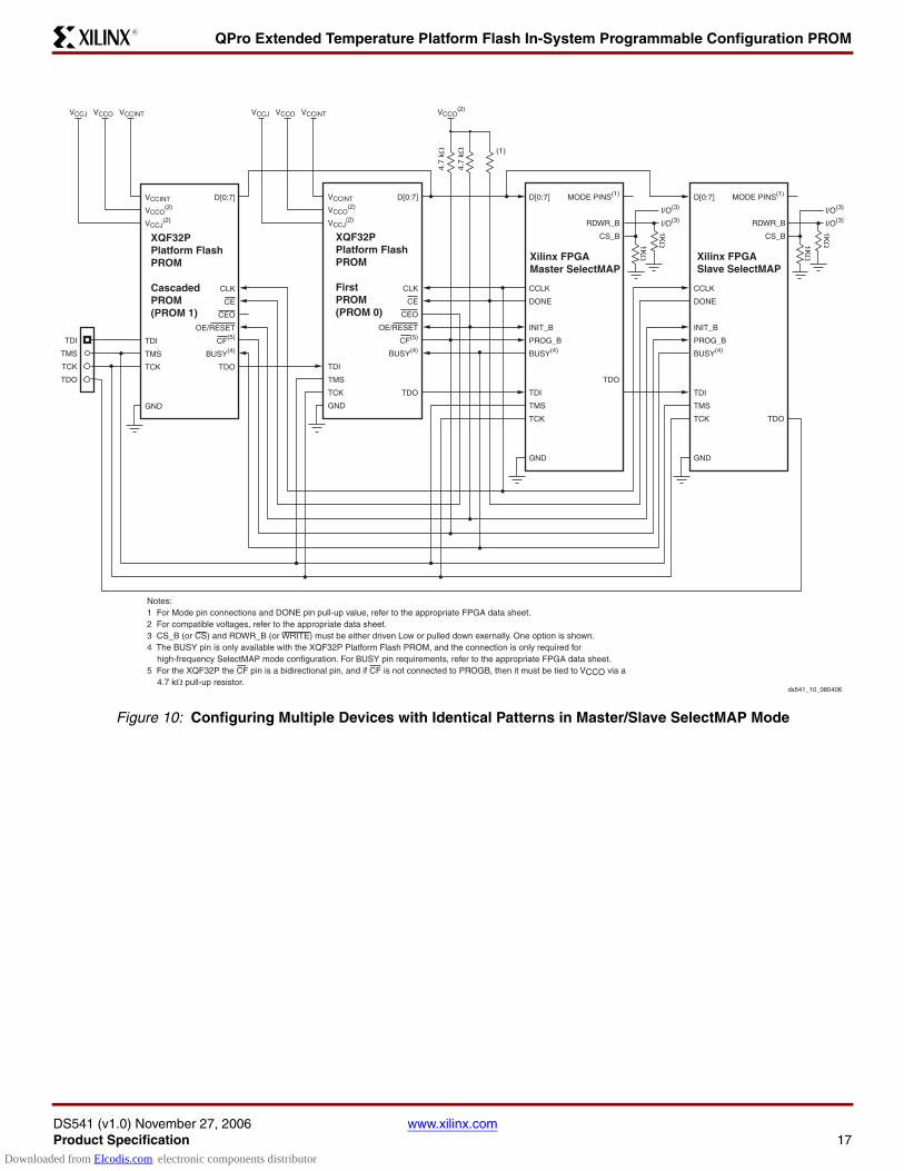
Figure 10: Configuring Multiple Devices with Identical Patterns in Master/Slave SelectMAP Mode
Notes:1 For Mode pin connections and DONE pin pull-up value, refer to the appropriate FPGA data sheet.2 For compatible voltages, refer to the appropriate data sheet.3 CS_B (or CS) and RDWR_B (or WRITE) must be either driven Low or pulled down exernally. One option is shown.4 The BUSY pin is only available with the XQF32P Platform Flash PROM, and the connection is only required for
high-frequency SelectMAP mode configuration. For BUSY pin requirements, refer to the appropriate FPGA data sheet.5 For the XQF32P the CF pin is a bidirectional pin, and if CF is not connected to PROGB, then it must be tied to VCCO via a
4.7 kΩ pull-up resistor.
XQF32PPlatform Flash PROM
First PROM(PROM 0)
VCCINT
VCCO(2)
VCCJ(2)
TDI
TMS
TCK
GND
D[0:7]
CLK
CE
CEO
OE/RESET
CF(5)
BUSY(4)
TDO
Xilinx FPGAMaster SelectMAP
D[0:7]
CCLK
DONE
INIT_B
PROG_B
BUSY(4)
TDI
TMS
TCK
GND
MODE PINS(1)
TDO
VCCJ VCCO VCCINT
4.7
kΩ
4.7
kΩ (1)
VCCO(2)
TDI
TMS
TCK
TDO
Xilinx FPGASlave SelectMAP
D[0:7]
CCLK
DONE
INIT_B
PROG_B
BUSY(4)
TDI
TMS
TCK
GND
XQF32PPlatform Flash PROM
Cascaded PROM(PROM 1)
VCCINT
VCCO(2)
VCCJ(2)
TDI
TMS
TCK
GND
D[0:7]
CLK
CE
CEO
OE/RESET
CF(5)
BUSY(4)
TDO
VCCJ VCCO VCCINT
MODE PINS(1)
TDO
ds541_10_080406
1KΩ1K
Ω
I/O(3)
I/O(3)
1KΩ1K
Ω
I/O(3)
I/O(3)RDWR_B
CS_B
RDWR_B
CS_B
Downloaded from Elcodis.com electronic components distributor
QPro Extended Temperature Platform Flash In-System Programmable Configuration PROM
DS541 (v1.0) November 27, 2006 www.xilinx.comProduct Specification 18
R
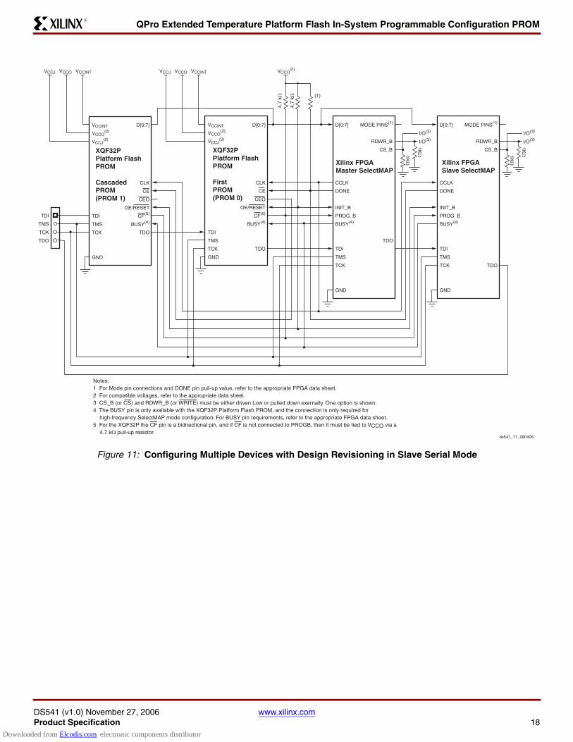
Figure 11: Configuring Multiple Devices with Design Revisioning in Slave Serial Mode
Notes:1 For Mode pin connections and DONE pin pull-up value, refer to the appropriate FPGA data sheet.2 For compatible voltages, refer to the appropriate data sheet.3 CS_B (or CS) and RDWR_B (or WRITE) must be either driven Low or pulled down exernally. One option is shown.4 The BUSY pin is only available with the XQF32P Platform Flash PROM, and the connection is only required for
high-frequency SelectMAP mode configuration. For BUSY pin requirements, refer to the appropriate FPGA data sheet.5 For the XQF32P the CF pin is a bidirectional pin, and if CF is not connected to PROGB, then it must be tied to VCCO via a
4.7 kΩ pull-up resistor.
XQF32PPlatform Flash PROM
First PROM(PROM 0)
VCCINT
VCCO(2)
VCCJ(2)
TDI
TMS
TCK
GND
D[0:7]
CLK
CE
CEO
OE/RESET
CF(5)
BUSY(4)
TDO
Xilinx FPGAMaster SelectMAP
D[0:7]
CCLK
DONE
INIT_B
PROG_B
BUSY(4)
TDI
TMS
TCK
GND
MODE PINS(1)
TDO
VCCJ VCCO VCCINT
4.7
kΩ
4.7
kΩ (1)
VCCO(2)
TDI
TMS
TCK
TDO
Xilinx FPGASlave SelectMAP
D[0:7]
CCLK
DONE
INIT_B
PROG_B
BUSY(4)
TDI
TMS
TCK
GND
XQF32PPlatform Flash PROM
Cascaded PROM(PROM 1)
VCCINT
VCCO(2)
VCCJ(2)
TDI
TMS
TCK
GND
D[0:7]
CLK
CE
CEO
OE/RESET
CF(5)
BUSY(4)
TDO
VCCJ VCCO VCCINT
MODE PINS(1)
TDO
ds541_11_080406
1KΩ1K
Ω
I/O(3)
I/O(3)
1KΩ1K
Ω
I/O(3)
I/O(3)RDWR_B
CS_B
RDWR_B
CS_B
Downloaded from Elcodis.com electronic components distributor
QPro Extended Temperature Platform Flash In-System Programmable Configuration PROM
DS541 (v1.0) November 27, 2006 www.xilinx.comProduct Specification 19
R
Figure 12: Configuring Multiple Devices with Design Revisioning in Slave SelectMAP Mode
Notes:1. For Mode pin connections and DONE pin pull-up value, refer to the appropriate FPGA data sheet.2. For compatible voltages, refer to the appropriate data sheet.3. RDWR_B (or WRITE) must be either driven Low or pulled down exernally. One option is shown.4. The BUSY pin is only available with the XQF32P Platform Flash PROM, and the connection is only required for high
frequency SelectMAP mode configuration. For BUSY pin requirements, refer to the appropriate FPGA data sheet.5. In Slave SelectMAP mode, the configuration interface can be clocked by an external oscillator, or optionally the
CLKOUT signal can be used to drive the FPGA's configuration clock (CCLK). If the XQF32P PROM's CLKOUT signal is used, then it must be tied to a 4.7KΩ resistor pulled up to VCCO.
6 For the XQF32P the CF pin is a bidirectional pin, and if CF is not connected to PROGB, then must be tied to VCCO via a 4.7 kΩ pull-up resistor
XQF32PPlatform Flash PROM
First PROM(PROM 0)
VCCINT
VCCO(2)
VCCJ(2)
TDI
TMS
TCK
EN_EXT_SEL
REV_SEL[1:0]
GND
D[0:7]
CLK(5)
CE
CEO
OE/RESET
CF(6)
BUSY(4)
TDO
Xilinx FPGASlave SelectMAP
D[0:7]
CCLK
DONE
INIT_B
PROG_B
BUSY(4)
TDI
TMS
TCK
MODE PINS(1)
RDWR_B
CS_B
TDO
VCCJ VCCO VCCINT
4.7
kΩ
4.7
kΩ
(1)
VCCO(2)
TDI
TMS
TCK
TDO
Xilinx FPGASlave SelectMAP
D[0:7]
CCLK
DONE
INIT_B
PROG_B
BUSY(4)
TDI
TMS
TCK
MODE PINS(1)
RDWR_B
CS_B
TDO
XQF32PPlatform Flash PROM
Cascaded PROM(PROM 1)
VCCINT
VCCO(2)
VCCJ(2)
TDI
TMS
TCK
EN_EXT_SEL
REV_SEL[1:0]
GND
D[0:7]
CLK(5)
CE
CEO
OE/RESET
CF(6)
BUSY(4)
TDO
VCCJ VCCO VCCINT
1KΩ
I/O(3)
1KΩ
I/O(3)
EN_EXT_SEL
REV_SEL[1:0]
CF
DONE
PROG_B
CS_B[1:0]
Design
Revision
Control
Logic
GND GND
ds541_12_070906
External (5)
Oscillator
Downloaded from Elcodis.com electronic components distributor
QPro Extended Temperature Platform Flash In-System Programmable Configuration PROM
DS541 (v1.0) November 27, 2006 www.xilinx.comProduct Specification 20
R
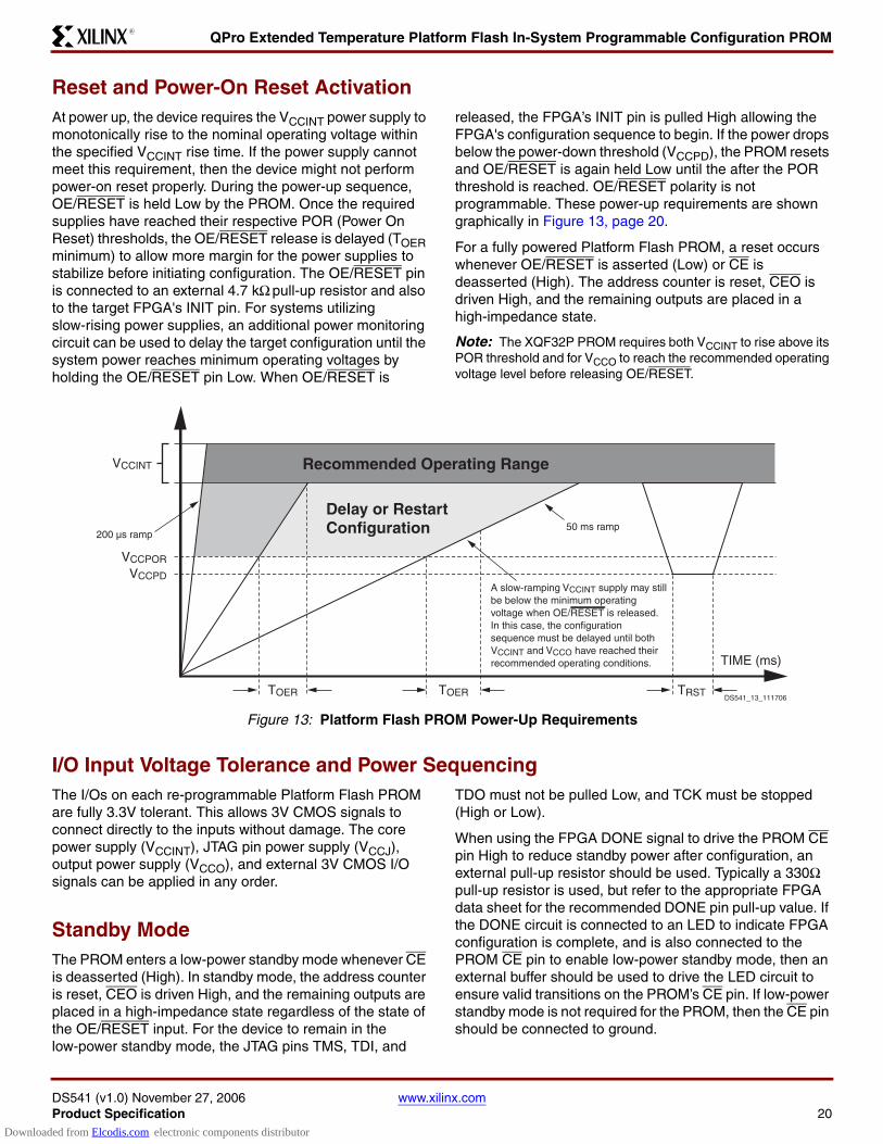
Reset and Power-On Reset ActivationAt power up, the device requires the VCCINT power supply to monotonically rise to the nominal operating voltage within the specified VCCINT rise time. If the power supply cannot meet this requirement, then the device might not perform power-on reset properly. During the power-up sequence, OE/RESET is held Low by the PROM. Once the required supplies have reached their respective POR (Power On Reset) thresholds, the OE/RESET release is delayed (TOER minimum) to allow more margin for the power supplies to stabilize before initiating configuration. The OE/RESET pin is connected to an external 4.7 kΩ pull-up resistor and also to the target FPGA's INIT pin. For systems utilizing slow-rising power supplies, an additional power monitoring circuit can be used to delay the target configuration until the system power reaches minimum operating voltages by holding the OE/RESET pin Low. When OE/RESET is
released, the FPGA’s INIT pin is pulled High allowing the FPGA's configuration sequence to begin. If the power drops below the power-down threshold (VCCPD), the PROM resets and OE/RESET is again held Low until the after the POR threshold is reached. OE/RESET polarity is not programmable. These power-up requirements are shown graphically in Figure 13, page 20.
For a fully powered Platform Flash PROM, a reset occurs whenever OE/RESET is asserted (Low) or CE is deasserted (High). The address counter is reset, CEO is driven High, and the remaining outputs are placed in a high-impedance state.
Note: The XQF32P PROM requires both VCCINT to rise above its POR threshold and for VCCO to reach the recommended operating voltage level before releasing OE/RESET.
I/O Input Voltage Tolerance and Power Sequencing The I/Os on each re-programmable Platform Flash PROM are fully 3.3V tolerant. This allows 3V CMOS signals to connect directly to the inputs without damage. The core power supply (VCCINT), JTAG pin power supply (VCCJ), output power supply (VCCO), and external 3V CMOS I/O signals can be applied in any order.
Standby ModeThe PROM enters a low-power standby mode whenever CE is deasserted (High). In standby mode, the address counter is reset, CEO is driven High, and the remaining outputs are placed in a high-impedance state regardless of the state of the OE/RESET input. For the device to remain in the low-power standby mode, the JTAG pins TMS, TDI, and
TDO must not be pulled Low, and TCK must be stopped (High or Low).
When using the FPGA DONE signal to drive the PROM CE pin High to reduce standby power after configuration, an external pull-up resistor should be used. Typically a 330Ω pull-up resistor is used, but refer to the appropriate FPGA data sheet for the recommended DONE pin pull-up value. If the DONE circuit is connected to an LED to indicate FPGA configuration is complete, and is also connected to the PROM CE pin to enable low-power standby mode, then an external buffer should be used to drive the LED circuit to ensure valid transitions on the PROM’s CE pin. If low-power standby mode is not required for the PROM, then the CE pin should be connected to ground.
Figure 13: Platform Flash PROM Power-Up Requirements
TOER
VCCINT
VCCPOR
VCCPD
200 µs ramp50 ms ramp
TOER TRST
TIME (ms)
A slow-ramping VCCINT supply may still be below the minimum operating voltage when OE/RESET is released. In this case, the configuration sequence must be delayed until both VCCINT and VCCO have reached their recommended operating conditions.
Recommended Operating Range
Delay or RestartConfiguration
DS541_13_111706
Downloaded from Elcodis.com electronic components distributor
QPro Extended Temperature Platform Flash In-System Programmable Configuration PROM
DS541 (v1.0) November 27, 2006 www.xilinx.comProduct Specification 21
R
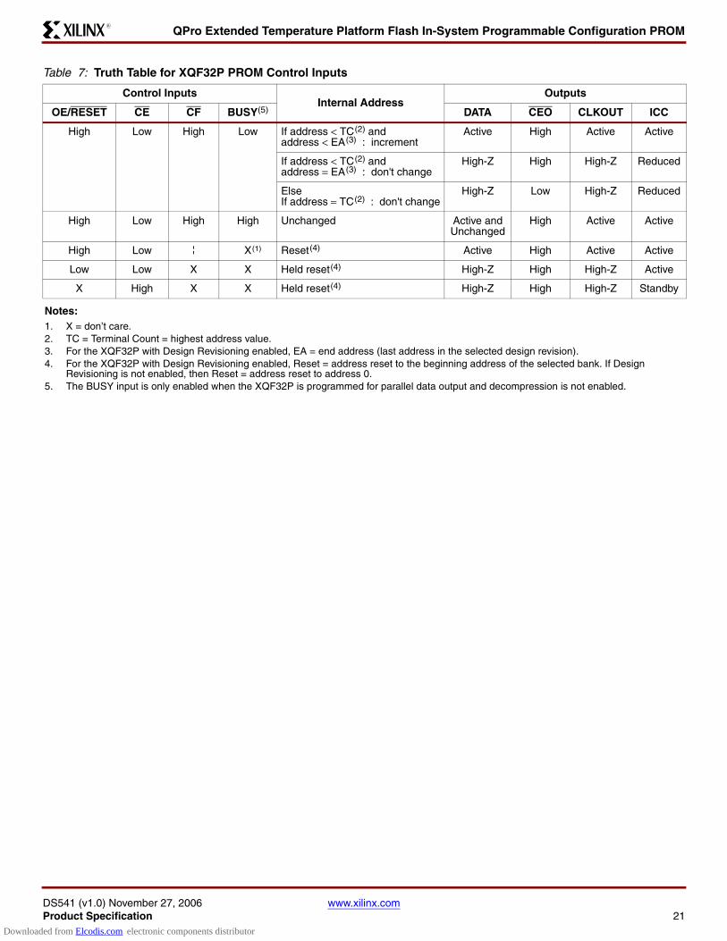
Table 7: Truth Table for XQF32P PROM Control Inputs
Control InputsInternal Address
Outputs
OE/RESET CE CF BUSY(5) DATA CEO CLKOUT ICC
High Low High Low If address < TC(2) and address < EA(3) : increment
Active High Active Active
If address < TC(2) and address = EA(3) : don't change
High-Z High High-Z Reduced
Else If address = TC(2) : don't change
High-Z Low High-Z Reduced
High Low High High Unchanged Active and Unchanged
High Active Active
High Low ¦ X(1) Reset(4) Active High Active Active
Low Low X X Held reset(4) High-Z High High-Z Active
X High X X Held reset(4) High-Z High High-Z Standby
Notes: 1. X = don’t care.2. TC = Terminal Count = highest address value.3. For the XQF32P with Design Revisioning enabled, EA = end address (last address in the selected design revision). 4. For the XQF32P with Design Revisioning enabled, Reset = address reset to the beginning address of the selected bank. If Design
Revisioning is not enabled, then Reset = address reset to address 0.5. The BUSY input is only enabled when the XQF32P is programmed for parallel data output and decompression is not enabled.
Downloaded from Elcodis.com electronic components distributor
QPro Extended Temperature Platform Flash In-System Programmable Configuration PROM
DS541 (v1.0) November 27, 2006 www.xilinx.comProduct Specification 22
R
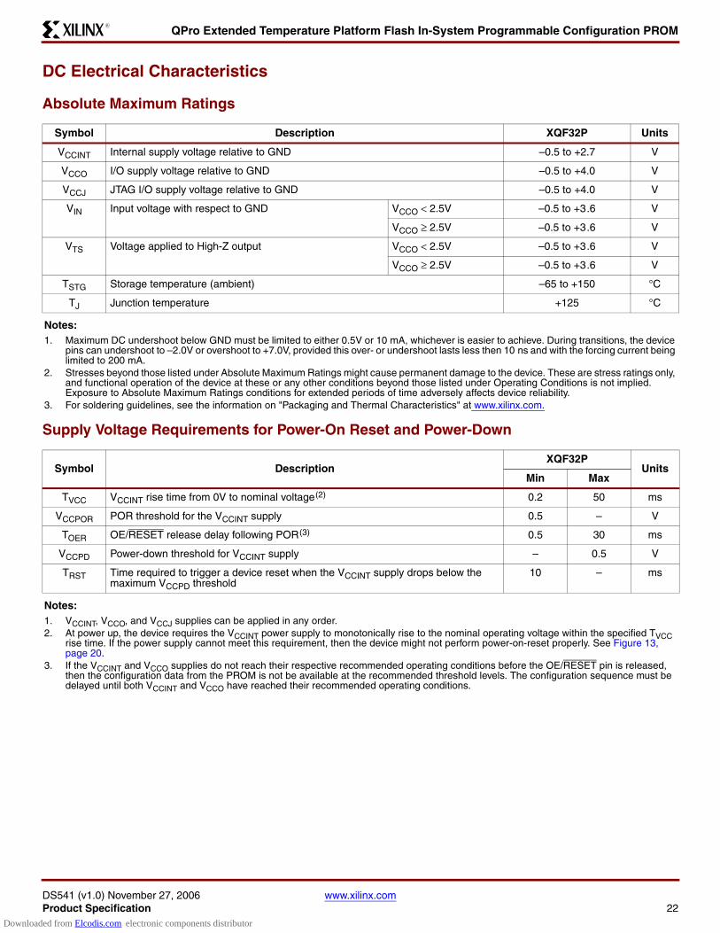
DC Electrical Characteristics
Absolute Maximum Ratings
Supply Voltage Requirements for Power-On Reset and Power-Down
Symbol Description XQF32P Units
VCCINT Internal supply voltage relative to GND –0.5 to +2.7 V
VCCO I/O supply voltage relative to GND –0.5 to +4.0 V
VCCJ JTAG I/O supply voltage relative to GND –0.5 to +4.0 V
VIN Input voltage with respect to GND VCCO < 2.5V –0.5 to +3.6 V
VCCO ≥ 2.5V –0.5 to +3.6 V
VTS Voltage applied to High-Z output VCCO < 2.5V –0.5 to +3.6 V
VCCO ≥ 2.5V –0.5 to +3.6 V
TSTG Storage temperature (ambient) –65 to +150 °C
TJ Junction temperature +125 °C
Notes: 1. Maximum DC undershoot below GND must be limited to either 0.5V or 10 mA, whichever is easier to achieve. During transitions, the device
pins can undershoot to –2.0V or overshoot to +7.0V, provided this over- or undershoot lasts less then 10 ns and with the forcing current being limited to 200 mA.
2. Stresses beyond those listed under Absolute Maximum Ratings might cause permanent damage to the device. These are stress ratings only, and functional operation of the device at these or any other conditions beyond those listed under Operating Conditions is not implied. Exposure to Absolute Maximum Ratings conditions for extended periods of time adversely affects device reliability.
3. For soldering guidelines, see the information on "Packaging and Thermal Characteristics" at www.xilinx.com.
Symbol DescriptionXQF32P
UnitsMin Max
TVCC VCCINT rise time from 0V to nominal voltage(2) 0.2 50 ms
VCCPOR POR threshold for the VCCINT supply 0.5 – V
TOER OE/RESET release delay following POR(3) 0.5 30 ms
VCCPD Power-down threshold for VCCINT supply – 0.5 V
TRST Time required to trigger a device reset when the VCCINT supply drops below the maximum VCCPD threshold
10 – ms
Notes: 1. VCCINT, VCCO, and VCCJ supplies can be applied in any order.2. At power up, the device requires the VCCINT power supply to monotonically rise to the nominal operating voltage within the specified TVCC
rise time. If the power supply cannot meet this requirement, then the device might not perform power-on-reset properly. See Figure 13, page 20.
3. If the VCCINT and VCCO supplies do not reach their respective recommended operating conditions before the OE/RESET pin is released, then the configuration data from the PROM is not be available at the recommended threshold levels. The configuration sequence must be delayed until both VCCINT and VCCO have reached their recommended operating conditions.
Downloaded from Elcodis.com electronic components distributor
QPro Extended Temperature Platform Flash In-System Programmable Configuration PROM
DS541 (v1.0) November 27, 2006 www.xilinx.comProduct Specification 23
R
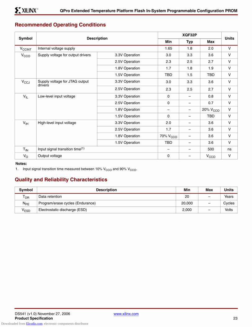
Recommended Operating Conditions
Quality and Reliability Characteristics
Symbol DescriptionXQF32P
UnitsMin Typ Max
VCCINT Internal voltage supply 1.65 1.8 2.0 V
VCCO Supply voltage for output drivers 3.3V Operation 3.0 3.3 3.6 V
2.5V Operation 2.3 2.5 2.7 V
1.8V Operation 1.7 1.8 1.9 V
1.5V Operation TBD 1.5 TBD V
VCCJ Supply voltage for JTAG output drivers
3.3V Operation 3.0 3.3 3.6 V
2.5V Operation 2.3 2.5 2.7 V
VIL Low-level input voltage 3.3V Operation 0 – 0.8 V
2.5V Operation 0 – 0.7 V
1.8V Operation – – 20% VCCO V
1.5V Operation 0 – TBD V
VIH High-level input voltage 3.3V Operation 2.0 – 3.6 V
2.5V Operation 1.7 – 3.6 V
1.8V Operation 70% VCCO – 3.6 V
1.5V Operation TBD – 3.6 V
TIN Input signal transition time(1) – – 500 ns
VO Output voltage 0 – VCCO V
Notes: 1. Input signal transition time measured between 10% VCCO and 90% VCCO.
Symbol Description Min Max Units
TDR Data retention 20 – Years
NPE Program/erase cycles (Endurance) 20,000 – Cycles
VESD Electrostatic discharge (ESD) 2,000 – Volts
Downloaded from Elcodis.com electronic components distributor
QPro Extended Temperature Platform Flash In-System Programmable Configuration PROM
DS541 (v1.0) November 27, 2006 www.xilinx.comProduct Specification 24
R
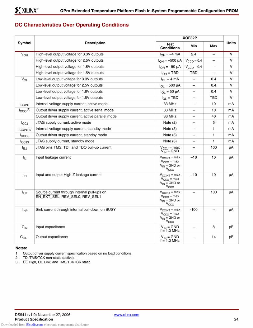
DC Characteristics Over Operating Conditions
Symbol DescriptionXQF32P
UnitsTest Conditions Min Max
VOH High-level output voltage for 3.3V outputs IOH = –4 mA 2.4 – V
High-level output voltage for 2.5V outputs IOH = –500 µA VCCO – 0.4 – V
High-level output voltage for 1.8V outputs IOH = –50 µA VCCO – 0.4 – V
High-level output voltage for 1.5V outputs IOH = TBD TBD – V
VOL Low-level output voltage for 3.3V outputs IOL = 4 mA – 0.4 V
Low-level output voltage for 2.5V outputs IOL = 500 µA – 0.4 V
Low-level output voltage for 1.8V outputs IOL = 50 µA – 0.4 V
Low-level output voltage for 1.5V outputs IOL = TBD – TBD V
ICCINT Internal voltage supply current, active mode 33 MHz – 10 mA
ICCO(1) Output driver supply current, active serial mode 33 MHz – 10 mA
Output driver supply current, active parallel mode 33 MHz – 40 mA
ICCJ JTAG supply current, active mode Note (2) – 5 mA
ICCINTS Internal voltage supply current, standby mode Note (3) – 1 mA
ICCOS Output driver supply current, standby mode Note (3) – 1 mA
ICCJS JTAG supply current, standby mode Note (3) – 1 mA
IILJ JTAG pins TMS, TDI, and TDO pull-up current VCCJ = maxVIN = GND
– 100 µA
IIL Input leakage current VCCINT = maxVCCO = maxVIN = GND or
VCCO
–10 10 µA
IIH Input and output High-Z leakage current VCCINT = maxVCCO = maxVIN = GND or
VCCO
–10 10 µA
IILP Source current through internal pull-ups onEN_EXT_SEL, REV_SEL0, REV_SEL1
VCCINT = maxVCCO = maxVIN = GND or
VCCO
– 100 µA
IIHP Sink current through internal pull-down on BUSY VCCINT = maxVCCO = maxVIN = GND or
VCCO
-100 – µA
CIN Input capacitance VIN = GNDf = 1.0 MHz
– 8 pF
COUT Output capacitance VIN = GNDf = 1.0 MHz
– 14 pF
Notes: 1. Output driver supply current specification based on no load conditions.2. TDI/TMS/TCK non-static (active).3. CE High, OE Low, and TMS/TDI/TCK static.
Downloaded from Elcodis.com electronic components distributor
QPro Extended Temperature Platform Flash In-System Programmable Configuration PROM
DS541 (v1.0) November 27, 2006 www.xilinx.comProduct Specification 25
R
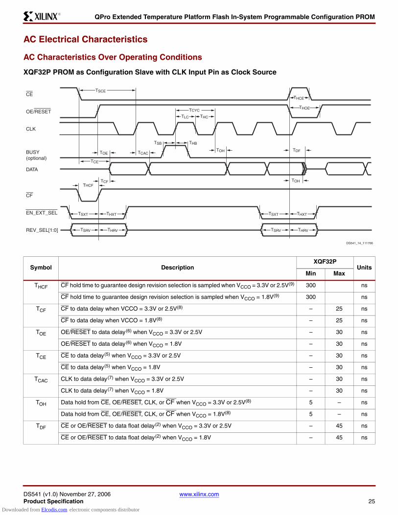
AC Electrical Characteristics
AC Characteristics Over Operating Conditions
XQF32P PROM as Configuration Slave with CLK Input Pin as Clock Source
Symbol DescriptionXQF32P
UnitsMin Max
THCF CF hold time to guarantee design revision selection is sampled when VCCO = 3.3V or 2.5V(9) 300 ns
CF hold time to guarantee design revision selection is sampled when VCCO = 1.8V(9) 300 ns
TCF CF to data delay when VCCO = 3.3V or 2.5V(8) – 25 ns
CF to data delay when VCCO = 1.8V(8) – 25 ns
TOE OE/RESET to data delay(6) when VCCO = 3.3V or 2.5V – 30 ns
OE/RESET to data delay(6) when VCCO = 1.8V – 30 ns
TCE CE to data delay(5) when VCCO = 3.3V or 2.5V – 30 ns
CE to data delay(5) when VCCO = 1.8V – 30 ns
TCAC CLK to data delay(7) when VCCO = 3.3V or 2.5V – 30 ns
CLK to data delay(7) when VCCO = 1.8V – 30 ns
TOH Data hold from CE, OE/RESET, CLK, or CF when VCCO = 3.3V or 2.5V(8) 5 – ns
Data hold from CE, OE/RESET, CLK, or CF when VCCO = 1.8V(8) 5 – ns
TDF CE or OE/RESET to data float delay(2) when VCCO = 3.3V or 2.5V – 45 ns
CE or OE/RESET to data float delay(2) when VCCO = 1.8V – 45 ns
CE
OE/RESET
CLK
BUSY(optional)
DATA
TCE
TLC THC
TSCE
TOE TCAC
THCE
THOETCYC
TOH
TDFTOH
THBTSB
CF
EN_EXT_SEL
REV_SEL[1:0]
TSXT THXT
TSRV THRV
DS541_14_111706
TSXT THXT
TSRV THRV
TCFTHCF
Downloaded from Elcodis.com electronic components distributor
QPro Extended Temperature Platform Flash In-System Programmable Configuration PROM
DS541 (v1.0) November 27, 2006 www.xilinx.comProduct Specification 26
R
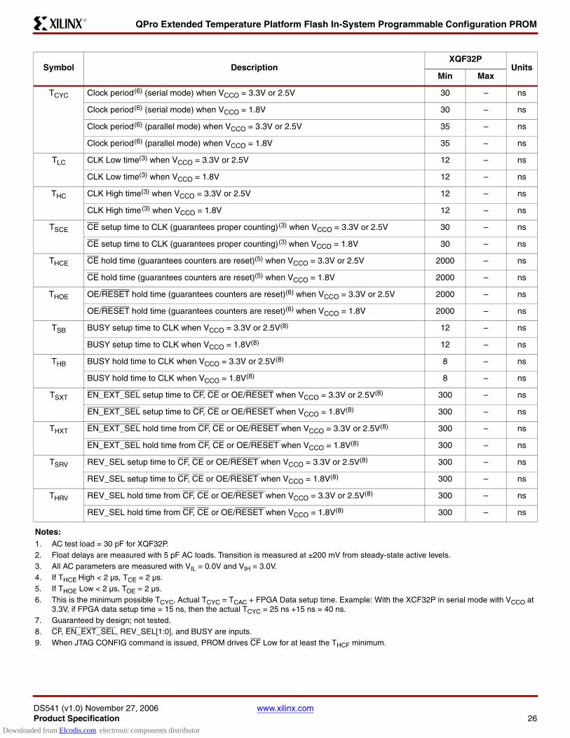
TCYC Clock period(6) (serial mode) when VCCO = 3.3V or 2.5V 30 – ns
Clock period(6) (serial mode) when VCCO = 1.8V 30 – ns
Clock period(6) (parallel mode) when VCCO = 3.3V or 2.5V 35 – ns
Clock period(6) (parallel mode) when VCCO = 1.8V 35 – ns
TLC CLK Low time(3) when VCCO = 3.3V or 2.5V 12 – ns
CLK Low time(3) when VCCO = 1.8V 12 – ns
THC CLK High time(3) when VCCO = 3.3V or 2.5V 12 – ns
CLK High time(3) when VCCO = 1.8V 12 – ns
TSCE CE setup time to CLK (guarantees proper counting)(3) when VCCO = 3.3V or 2.5V 30 – ns
CE setup time to CLK (guarantees proper counting)(3) when VCCO = 1.8V 30 – ns
THCE CE hold time (guarantees counters are reset)(5) when VCCO = 3.3V or 2.5V 2000 – ns
CE hold time (guarantees counters are reset)(5) when VCCO = 1.8V 2000 – ns
THOE OE/RESET hold time (guarantees counters are reset)(6) when VCCO = 3.3V or 2.5V 2000 – ns
OE/RESET hold time (guarantees counters are reset)(6) when VCCO = 1.8V 2000 – ns
TSB BUSY setup time to CLK when VCCO = 3.3V or 2.5V(8) 12 – ns
BUSY setup time to CLK when VCCO = 1.8V(8) 12 – ns
THB BUSY hold time to CLK when VCCO = 3.3V or 2.5V(8) 8 – ns
BUSY hold time to CLK when VCCO = 1.8V(8) 8 – ns
TSXT EN_EXT_SEL setup time to CF, CE or OE/RESET when VCCO = 3.3V or 2.5V(8) 300 – ns
EN_EXT_SEL setup time to CF, CE or OE/RESET when VCCO = 1.8V(8) 300 – ns
THXT EN_EXT_SEL hold time from CF, CE or OE/RESET when VCCO = 3.3V or 2.5V(8) 300 – ns
EN_EXT_SEL hold time from CF, CE or OE/RESET when VCCO = 1.8V(8) 300 – ns
TSRV REV_SEL setup time to CF, CE or OE/RESET when VCCO = 3.3V or 2.5V(8) 300 – ns
REV_SEL setup time to CF, CE or OE/RESET when VCCO = 1.8V(8) 300 – ns
THRV REV_SEL hold time from CF, CE or OE/RESET when VCCO = 3.3V or 2.5V(8) 300 – ns
REV_SEL hold time from CF, CE or OE/RESET when VCCO = 1.8V(8) 300 – ns
Notes: 1. AC test load = 30 pF for XQF32P.2. Float delays are measured with 5 pF AC loads. Transition is measured at ±200 mV from steady-state active levels.3. All AC parameters are measured with VIL = 0.0V and VIH = 3.0V.4. If THCE High < 2 µs, TCE = 2 µs.5. If THOE Low < 2 µs, TOE = 2 µs.6. This is the minimum possible TCYC. Actual TCYC = TCAC + FPGA Data setup time. Example: With the XCF32P in serial mode with VCCO at
3.3V, if FPGA data setup time = 15 ns, then the actual TCYC = 25 ns +15 ns = 40 ns.7. Guaranteed by design; not tested.8. CF, EN_EXT_SEL, REV_SEL[1:0], and BUSY are inputs.9. When JTAG CONFIG command is issued, PROM drives CF Low for at least the THCF minimum.
Symbol DescriptionXQF32P
UnitsMin Max
Downloaded from Elcodis.com electronic components distributor
QPro Extended Temperature Platform Flash In-System Programmable Configuration PROM
DS541 (v1.0) November 27, 2006 www.xilinx.comProduct Specification 27
R
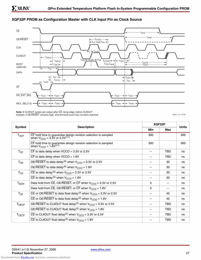
XQF32P PROM as Configuration Master with CLK Input Pin as Clock Source
Symbol DescriptionXQF32P
UnitsMin Max
THCF CF hold time to guarantee design revision selection is sampledwhen VCCO = 3.3V or 2.5V(11)
300 300
CF hold time to guarantee design revision selection is sampledwhen VCCO = 1.8V(11)
300 300
TCF CF to data delay when VCCO = 3.3V or 2.5V – TBD ns
CF to data delay when VCCO = 1.8V – TBD ns
TOE OE/RESET to data delay(6) when VCCO = 3.3V or 2.5V – 30 ns
OE/RESET to data delay(6) when VCCO = 1.8V – 30 ns
TCE CE to data delay(5) when VCCO = 3.3V or 2.5V – 30 ns
CE to data delay(5) when VCCO = 1.8V – 30 ns
TEOH Data hold from CE, OE/RESET, or CF when VCCO = 3.3V or 2.5V 5 – ns
Data hold from CE, OE/RESET, or CF when VCCO = 1.8V 5 – ns
TDF CE or OE/RESET to data float delay(2) when VCCO = 3.3V or 2.5V – 45 ns
CE or OE/RESET to data float delay(2) when VCCO = 1.8V – 45 ns
TOECF OE/RESET to CLKOUT float delay(2) when VCCO = 3.3V or 2.5V – TBD ns
OE/RESET to CLKOUT float delay(2) when VCCO = 1.8V – TBD ns
TCECF CE to CLKOUT float delay(2) when VCCO = 3.3V or 2.5V – TBD ns
CE to CLKOUT float delay(2) when VCCO = 1.8V – TBD ns
CE
OE/RESET
CLK
CLKOUT
BUSY(optional)
DATA
TCE
TLC THC
TOE
THCE
THOETCYCO
THBTSBTOECC
TCECC
TCLKO
TCOH
TCCDD
DS541_15_111706
TEOH
TDF
Note: 8 CLKOUT cycles are output after CE rising edge, before CLKOUT tristates, if OE/RESET remains high, and terminal count has not been reached.
CF
EN_EXT_SEL
REV_SEL[1:0]
TSXT THXT
TSRV THRV
TSXT THXT
TSRV THRV
TCF
TCFCC
TCECFTOECF
TDDC
THCF
Downloaded from Elcodis.com electronic components distributor
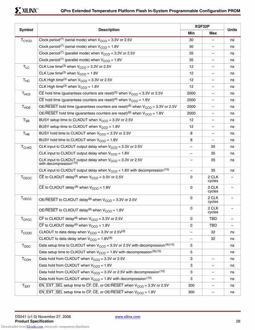
QPro Extended Temperature Platform Flash In-System Programmable Configuration PROM
DS541 (v1.0) November 27, 2006 www.xilinx.comProduct Specification 28
R
TCYCO Clock period(7) (serial mode) when VCCO = 3.3V or 2.5V 30 – ns
Clock period(7) (serial mode) when VCCO = 1.8V 30 – ns
Clock period(7) (parallel mode) when VCCO = 3.3V or 2.5V 35 – ns
Clock period(7) (parallel mode) when VCCO = 1.8V 35 – ns
TLC CLK Low time(3) when VCCO = 3.3V or 2.5V 12 – ns
CLK Low time(3) when VCCO = 1.8V 12 – ns
THC CLK High time(3) when VCCO = 3.3V or 2.5V 12 – ns
CLK High time(3) when VCCO = 1.8V 12 – ns
THCE CE hold time (guarantees counters are reset)(5) when VCCO = 3.3V or 2.5V 2000 – ns
CE hold time (guarantees counters are reset)(5) when VCCO = 1.8V 2000 – ns
THOE OE/RESET hold time (guarantees counters are reset)(6) when VCCO = 3.3V or 2.5V 2000 – ns
OE/RESET hold time (guarantees counters are reset)(6) when VCCO = 1.8V 2000 – ns
TSB BUSY setup time to CLKOUT when VCCO = 3.3V or 2.5V 12 – ns
BUSY setup time to CLKOUT when VCCO = 1.8V 12 – ns
THB BUSY hold time to CLKOUT when VCCO = 3.3V or 2.5V 8 – ns
BUSY hold time to CLKOUT when VCCO = 1.8V 8 – ns
TCLKO CLK input to CLKOUT output delay when VCCO = 3.3V or 2.5V – 35 ns
CLK input to CLKOUT output delay when VCCO = 1.8V – 35 ns
CLK input to CLKOUT output delay when VCCO = 3.3V or 2.5Vwith decompression(10)
– 35 ns
CLK input to CLKOUT output delay when VCCO = 1.8V with decompression(10) – 35 ns
TCECC CE to CLKOUT delay(8) when VCCO = 3.3V or 2.5V 0 2 CLK cycles
–
CE to CLKOUT delay(8) when VCCO = 1.8V 0 2 CLK cycles
–
TOECC OE/RESET to CLKOUT delay(8) when VCCO = 3.3V or 2.5V 0 2 CLK cycles
–
OE/RESET to CLKOUT delay(8) when VCCO = 1.8V 0 2 CLK cycles
–
TCFCC CF to CLKOUT delay(8) when VCCO = 3.3V or 2.5V 0 TBD –
CF to CLKOUT delay(8) when VCCO = 1.8V 0 TBD –
TCCDD CLKOUT to data delay when VCCO = 3.3V or 2.5V(9) – 32 ns
CLKOUT to data delay when VCCO = 1.8V(9) – 32 ns
TDDC Data setup time to CLKOUT when VCCO = 3.3V or 2.5V with decompression(9)(10) 5 ns
Data setup time to CLKOUT when VCCO = 1.8V with decompression(9)(10) 5 ns
TCOH Data hold from CLKOUT when VCCO = 3.3V or 2.5V 3 – ns
Data hold from CLKOUT when VCCO = 1.8V 3 – ns
Data hold from CLKOUT when VCCO = 3.3V or 2.5V with decompression(10) 3 – ns
Data hold from CLKOUT when VCCO = 1.8V with decompression(10) 3 – ns
TSXT EN_EXT_SEL setup time to CF, CE, or OE/RESET when VCCO = 3.3V or 2.5V 300 – ns
EN_EXT_SEL setup time to CF, CE, or OE/RESET when VCCO = 1.8V 300 – ns
Symbol DescriptionXQF32P
UnitsMin Max
Downloaded from Elcodis.com electronic components distributor

QPro Extended Temperature Platform Flash In-System Programmable Configuration PROM
DS541 (v1.0) November 27, 2006 www.xilinx.comProduct Specification 29
R
THXT EN_EXT_SEL hold time from CF, CE, or OE/RESET when VCCO = 3.3V or 2.5V 300 – ns
EN_EXT_SEL hold time from CF, CE, or OE/RESET when VCCO = 1.8V 300 – ns
TSRV REV_SEL setup time to CF, CE, or OE/RESET when VCCO = 3.3V or 2.5V 300 – ns
REV_SEL setup time to CF, CE, or OE/RESET when VCCO = 1.8V 300 – ns
THRV REV_SEL hold time from CF, CE, or OE/RESET when VCCO = 3.3V or 2.5V 300 – ns
REV_SEL hold time from CF, CE, or OE/RESET when VCCO = 1.8V 300 – ns
Notes: 1. AC test load = 30 pF for XQF32P.2. Float delays are measured with 5 pF AC loads.Transition is measured at ±200 mV from steady-state active levels.3. Guaranteed by design, not tested.4. All AC parameters are measured with VIL = 0.0V and VIH = 3.0V.5. If THCE High < 2 µs, TCE = 2 µs.6. If THOE Low < 2 µs, TOE = 2 µs.7. This is the minimum possible TCYCO. Actual TCYCO = TCCDD + FPGA Data setup time. Example: With the XQF32P in serial mode with VCCO
at 3.3V, if FPGA Data setup time = 15 ns, then the actual TCYCO = 25 ns +15 ns = 40 ns.8. The delay before the enabled CLKOUT signal begins clocking data out of the device is dependent on the clocking configuration. The delay
before CLKOUT is enabled increases if decompression is enabled. 9. Slower CLK frequency option can be required to meet the FPGA data sheet setup time.10. When decompression is enabled, the CLKOUT signal becomes a controlled clock output. When decompressed data is available, CLKOUT
toggles at ½ the source clock frequency (either ½ the selected internal clock frequency or ½ the external CLK input frequency). When decompressed data is not available, the CLKOUT pin is parked High. If CLKOUT is used, then it must be pulled High externally using a 4.7kΩ pull-up to VCCO.
11. When JTAG CONFIG command is issued, PROM drives CF Low for at least the THCF minimum.
Symbol DescriptionXQF32P
UnitsMin Max
Downloaded from Elcodis.com electronic components distributor
QPro Extended Temperature Platform Flash In-System Programmable Configuration PROM
DS541 (v1.0) November 27, 2006 www.xilinx.comProduct Specification 30
R
XQF32P PROM as Configuration Master with Internal Oscillator as Clock Source
Symbol DescriptionXQF32P
UnitsMin Max
THCF CF hold time to guarantee design revision selection is sampledwhen VCCO = 3.3V or 2.5V(12)
300 300
CF hold time to guarantee design revision selection is sampledwhen VCCO = 1.8V(12)
300 300
TCF CF to data delay when VCCO = 3.3V or 2.5V – TBD ns
CF to data delay when VCCO = 1.8V – TBD ns
TOE OE/RESET to data delay(6) when VCCO = 3.3V or 2.5V – 30 ns
OE/RESET to data delay(6) when VCCO = 1.8V – 30 ns
TCE CE to data delay(5) when VCCO = 3.3V or 2.5V – 30 ns
CE to data delay(5) when VCCO = 1.8V – 30 ns
TEOH Data hold from CE, OE/RESET, or CF when VCCO = 3.3V or 2.5V 5 – ns
Data hold from CE, OE/RESET, or CF when VCCO = 1.8V 5 – ns
TDF CE or OE/RESET to data float delay(2) when VCCO = 3.3V or 2.5V – 45 ns
CE or OE/RESET to data float delay(2) when VCCO = 1.8V – 45 ns
TOECF OE/RESET to CLKOUT float delay(2) when VCCO = 3.3V or 2.5V – TBD ns
OE/RESET to CLKOUT float delay(2) when VCCO = 1.8V – TBD ns
TCECF CE to CLKOUT float delay(2) when VCCO = 3.3V or 2.5V – TBD ns
CE to CLKOUT float delay(2) when VCCO = 1.8V – TBD ns
THCE CE hold time (guarantees counters are reset)(5) when VCCO = 3.3V or 2.5V 2000 – ns
CE hold time (guarantees counters are reset)(5) when VCCO = 1.8V 2000 – ns
THOE OE/RESET hold time (guarantees counters are reset)(6) when VCCO = 3.3V or 2.5V 2000 – ns
OE/RESET hold time (guarantees counters are reset)(6) when VCCO = 1.8V 2000 – ns
TSB BUSY setup time to CLKOUT when VCCO = 3.3V or 2.5V 12 – ns
BUSY setup time to CLKOUT when VCCO = 1.8V 12 – ns
CE
OE/RESET
CLKOUT
BUSY(optional)
DATA
TCE
TOE
THCE
THOE
THBTSBTOEC
TCEC
TCOH
TCDD
DS541_16_111706
TEOH
TDF
Note: 8 CLKOUT cycles are output after CE rising edge, before CLKOUT tristates, if OE/RESET remains high, and terminal count has not been reached.
CF
EN_EXT_SEL
REV_SEL[1:0]
TSXT THXT
TSRV THRV
TSXT THXT
TSRV THRV
TCF
TCFC
TCECFTOECF
TDDC
THCF
Downloaded from Elcodis.com electronic components distributor
QPro Extended Temperature Platform Flash In-System Programmable Configuration PROM
DS541 (v1.0) November 27, 2006 www.xilinx.comProduct Specification 31
R
THB BUSY hold time to CLKOUT when VCCO = 3.3V or 2.5V 8 – ns
BUSY hold time to CLKOUT when VCCO = 1.8V 8 – ns
TCEC CE to CLKOUT delay(7) when VCCO = 3.3V or 2.5V 0 1 µs
CE to CLKOUT delay(7) when VCCO = 1.8V 0 1 µs
TOEC OE/RESET to CLKOUT delay(7) when VCCO = 3.3V or 2.5V 0 1 µs
OE/RESET to CLKOUT delay(7) when VCCO = 1.8V 0 1 µs
TCFC CF to CLKOUT delay(7) when VCCO = 3.3V or 2.5V 0 TBD –
CF to CLKOUT delay(7) when VCCO = 1.8V 0 TBD –
TCDD CLKOUT to data delay when VCCO = 3.3V or 2.5V(8) – 30 ns
CLKOUT to data delay when VCCO = 1.8V(8) – 30 ns
TDDC Data setup time to CLKOUT when VCCO = 3.3V or 2.5V with decompression(8)(11) 5 ns
Data setup time to CLKOUT when VCCO = 1.8V with decompression(8)(11) 5 ns
TCOH Data hold from CLKOUT when VCCO = 3.3V or 2.5V 3 – ns
Data hold from CLKOUT when VCCO = 1.8V 3 – ns
Data hold from CLKOUT when VCCO = 3.3V or 2.5V with decompression(11) 3 – ns
Data hold from CLKOUT when VCCO = 1.8V with decompression(11) 3 – ns
TSXT EN_EXT_SEL setup time to CF, CE, or OE/RESET when VCCO = 3.3V or 2.5V 300 – ns
EN_EXT_SEL setup time to CF, CE, or OE/RESET when VCCO = 1.8V 300 – ns
THXT EN_EXT_SEL hold time from CF, CE, or OE/RESET when VCCO = 3.3V or 2.5V 300 – ns
EN_EXT_SEL hold time from CF, CE, or OE/RESET when VCCO = 1.8V 300 – ns
TSRV REV_SEL setup time to CF, CE, or OE/RESET when VCCO = 3.3V or 2.5V 300 – ns
REV_SEL setup time to CF, CE, or OE/RESET when VCCO = 1.8V 300 – ns
THRV REV_SEL hold time from CF, CE, or OE/RESET when VCCO = 3.3V or 2.5V 300 – ns
REV_SEL hold time from CF, CE, or OE/RESET when VCCO = 1.8V 300 – ns
FF CLKOUT default (fast) frequency(9) 25 50 MHz
CLKOUT default (fast) frequency with decompression(11) 12.5 25 MHz
FS CLKOUT alternate (slower) frequency(10) 12.5 25 MHz
CLKOUT alternate (slower) frequency with decompression(11) 6 12.5 MHz
Notes: 1. AC test load = 30 pF for XQF32P.2. Float delays are measured with 5 pF AC loads. Transition is measured at ±200 mV from steady-state active levels.3. Guaranteed by design, not tested.4. All AC parameters are measured with VIL = 0.0V and VIH = 3.0V.5. If THCE High < 2 µs, TCE = 2 µs.6. If THOE Low < 2 µs, TOE = 2 µs.7. The delay before the enabled CLKOUT signal begins clocking data out of the device is dependent on the clocking configuration. The delay
before CLKOUT is enabled increases if decompression is enabled. 8. Slower CLK frequency option can be required to meet the FPGA data sheet setup time.9. Typical CLKOUT default (fast) period = 25 ns (40 MHz)10. Typical CLKOUT alternate (slower) period = 50 ns (20 MHz)11. When decompression is enabled, the CLKOUT signal becomes a controlled clock output. When decompressed data is available, CLKOUT
toggles at ½ the source clock frequency (either ½ the selected internal clock frequency or ½ the external CLK input frequency). When decompressed data is not available, the CLKOUT pin is parked High. If CLKOUT is used, then it must be pulled High externally using a 4.7kΩ pull-up to VCCO.
12. When JTAG CONFIG command is issued, PROM drives CF Low for at least the THCF minimum.
Symbol DescriptionXQF32P
UnitsMin Max
Downloaded from Elcodis.com electronic components distributor
QPro Extended Temperature Platform Flash In-System Programmable Configuration PROM
DS541 (v1.0) November 27, 2006 www.xilinx.comProduct Specification 32
R
AC Characteristics Over Operating Conditions When Cascading
Symbol DescriptionXQF32P
UnitsMin Max
TCDF CLK to output float delay(2,3) when VCCO = 2.5V or 3.3V – 25 ns
CLK to output float delay(2,3) when VCCO = 1.8V – 25 ns
TOCK CLK to CEO delay(3,5) when VCCO = 2.5V or 3.3V – 20 ns
CLK to CEO delay(3,5) when VCCO = 1.8V – 20 ns
TOCE CE to CEO delay(3,6) when VCCO = 2.5V or 3.3V – 80 ns
CE to CEO delay(3,6) when VCCO = 1.8V – 80 ns
TOOE OE/RESET to CEO delay(3) when VCCO = 2.5V or 3.3V – 80 ns
OE/RESET to CEO delay(3) when VCCO = 1.8V – 80 ns
TCOCE CLKOUT to CEO delay when VCCO = 2.5V or 3.3V – 25 ns
CLKOUT to CEO delay when VCCO = 1.8V – 25 ns
TCODF CLKOUT to output float delay when VCCO = 2.5V or 3.3V – 30 ns
CLKOUT to output float delay when VCCO = 1.8V – 30 ns
Notes: 1. AC test load = 30 pF for XQF32P.2. Float delays are measured with 5 pF AC loads. Transition is measured at ±200 mV from steady state active levels.3. Guaranteed by design, not tested.4. All AC parameters are measured with VIL = 0.0V and VIH = 3.0V.5. For cascaded PROMs, if the FPGA’s dual-purpose configuration data pins are set to persist as configuration pins, the minimum
period is increased based on the CLK to CEO and CE to data propagation delays:- TCYC minimum = TOCK + TCE + FPGA Data setup time.- TCAC maximum = TOCK + TCE
6. For cascaded PROMs, if the FPGA’s dual-purpose configuration data pins become general I/O pins after configuration; to allow for the disable to propagate to the cascaded PROMs and to avoid contention on the data lines following configuration, the minimum period is increased based on the CE to CEO and CE to data propagation delays:- TCYC minimum = TOCE + TCE - TCAC maximum = TOCK + TCE
OE/RESET
CE
CLK
CLKOUT(optional)
DATA
CEO
TOCETOOE
First BitLast Bit
TCDFTCODF
TOCK TCOCE
DS541_17_111706
Downloaded from Elcodis.com electronic components distributor
QPro Extended Temperature Platform Flash In-System Programmable Configuration PROM
DS541 (v1.0) November 27, 2006 www.xilinx.comProduct Specification 33
R
Pinouts and Pin Descriptions
XQF32P VO48 Pin Names and Descriptions
The XQF32P Platform Flash PROM is available in the VO48 package. Table 8 provides a list of the pin names anddescriptions for the XQF32P 48-pin VO48 plastic, thin, small outline package (TSOP).
Table 8: XQF32P Pin Names and Descriptions (VO48)
Pin Name Boundary Scan Order
Boundary Scan
FunctionPin Description
48-pin TSOP (VO48)
D0 28 Data Out D0 is the DATA output pin to provide data for configuring an FPGA in serial mode. D0-D7 are the DATA output pins to provide parallel data for configuring a Xilinx FPGA in SelectMap (parallel) mode. The D0 output is set to a high-impedance state during ISPEN (when not clamped).The D1-D7 outputs are set to a high-impedance state during ISPEN (when not clamped) and when serial mode is selected for configuration. The D1-D7 pins can be left unconnected when the PROM is used in serial mode.
28
27 Output Enable
D1 26 Data Out 29
25 Output Enable
D2 24 Data Out 32
23 Output Enable
D3 22 Data Out 33
21 Output Enable
D4 20 Data Out 43
19 Output Enable
D5 18 Data Out 44
17 Output Enable
D6 16 Data Out 47
15 Output Enable
D7 14 Data Out 48
13 Output Enable
CLK 01 Data In Configuration Clock Input. An internal programmable control bit selects between the internal oscillator and the CLK input pin as the clock source to control the configuration sequence. Each rising edge on the CLK input increments the internal address counter if the CLK input is selected, CE is Low, OE/RESET is High, BUSY is Low (parallel mode only), and CF is High.
12
OE/RESET 04 Data In Output Enable/Reset (Open-Drain I/O).When Low, this input holds the address counter reset and the DATA and CLKOUT outputs are placed in a high-impedance state. This is a bidirectional open-drain pin that is held Low while the PROM completes the internal power-on reset sequence. Polarity is not programmable.
11
03 Data Out
02 Output Enable
CE 00 Data In Chip Enable Input. When CE is High, the device is put into low-power standby mode, the address counter is reset, and the DATA and CLKOUT outputs are placed in a high-impedance state.
13
CF 11 Data In Configuration Pulse (Open-Drain I/O). As an output, this pin allows the JTAG CONFIG instruction to initiate FPGA configuration without powering down the FPGA. This is an open-drain signal that is pulsed Low by the JTAG CONFIG command. As an input, on the rising edge of CF, the current design revision selection is sampled and the internal address counter is reset to the start address for the selected revision. If unused, the CF pin must be pulled High using an external 4.7 KΩ pull-up to VCCO.
6
10 Data Out
09 Output Enable
CEO 06 Data Out Chip Enable Output. Chip Enable Output (CEO) is connected to the CE input of the next PROM in the chain. This output is Low when CE is Low and OE/RESET input is High, AND the internal address counter has been incremented beyond its Terminal Count (TC) value. CEO returns to High when OE/RESET goes Low or CE goes High.
10
05 Output Enable
Downloaded from Elcodis.com electronic components distributor
QPro Extended Temperature Platform Flash In-System Programmable Configuration PROM
DS541 (v1.0) November 27, 2006 www.xilinx.comProduct Specification 34
R
EN_EXT_SEL 31 Data In Enable External Selection Input. When this pin is Low, design revision selection is controlled by the Revision Select pins. When this pin is High, design revision selection is controlled by the internal programmable Revision Select control bits. EN_EXT_SEL has an internal 50KΩ resistive pull-up to VCCO to provide a logic 1 to the device if the pin is not driven.
25
REV_SEL0 30 Data In Revision Select[1:0] Inputs. When the EN_EXT_SEL is Low, the Revision Select pins are used to select the design revision to be enabled, overriding the internal programmable Revision Select control bits. The Revision Select[1:0] inputs have an internal 50 KΩ resistive pull-up to VCCO to provide a logic 1 to the device if the pins are not driven.
26
REV_SEL1 29 Data In 27
BUSY 12 Data In Busy Input. The BUSY input is enabled when parallel mode is selected for configuration. When BUSY is High, the internal address counter stops incrementing and the current data remains on the data pins. On the first rising edge of CLK after BUSY transitions from High to Low, the data for the next address is driven on the data pins. When serial mode or decompression is enabled during device programming, the BUSY input is disabled. BUSY has an internal 50 KΩ resistive pull-down to GND to provide a logic 0 to the device if the pin is not driven.
5
CLKOUT 08 Data Out Configuration Clock Output. An internal Programmable control bit enables the CLKOUT signal, which is sourced from either the internal oscillator or the CLK input pin. Each rising edge of the selected clock source increments the internal address counter if data is available, CE is Low, and OE/RESET is High. Output data is available on the rising edge of CLKOUT. CLKOUT is disabled if CE is High or OE/RESET is Low. If decompression is enabled, CLKOUT is parked High when decompressed data is not ready. When CLKOUT is disabled, the CLKOUT pin is put into a high-Z state. If CLKOUT is used, then it must be pulled High externally using a 4.7 KΩ pull-up to VCCO.
9
07 Output Enable
TMS Mode Select JTAG Mode Select Input. The state of TMS on the rising edge of TCK determines the state transitions at the Test Access Port (TAP) controller. TMS has an internal 50 KΩ resistive pull-up to VCCJ to provide a logic 1 to the device if the pin is not driven.
21
TCK Clock JTAG Clock Input. This pin is the JTAG test clock. It sequences the TAP controller and all the JTAG test and programming electronics.
20
TDI Data In JTAG Serial Data Input. This pin is the serial input to all JTAG instruction and data registers. TDI has an internal 50 KΩ resistive pull-up to VCCJ to provide a logic 1 to the device if the pin is not driven.
19
TDO Data Out JTAG Serial Data Output. This pin is the serial output for all JTAG instruction and data registers. TDO has an internal 50KΩ resistive pull-up to VCCJ to provide a logic 1 to the system if the pin is not driven.
22
VCCINT +1.8V Supply. Positive 1.8V supply voltage for internal logic. 4, 15, 34
VCCO +3.3V, 2.5V, or 1.8V I/O Supply. Positive 3.3V, 2.5V, or 1.8V supply voltage connected to the output voltage drivers and input buffers.
8, 30, 38, 45
VCCJ +3.3V or 2.5V JTAG I/O Supply. Positive 3.3V, 2.5V, or 1.8V supply voltage connected to the TDO output voltage driver and TCK, TMS, and TDI input buffers.
24
GND Ground 2, 7, 17, 23,
31, 36, 46
DNC Do Not Connect. (These pins must be left unconnected.) 1, 3, 14, 16,
18, 35, 37, 39, 40, 41,
42
Table 8: XQF32P Pin Names and Descriptions (VO48) (Continued)
Pin Name Boundary Scan Order
Boundary Scan
FunctionPin Description
48-pin TSOP (VO48)
Downloaded from Elcodis.com electronic components distributor
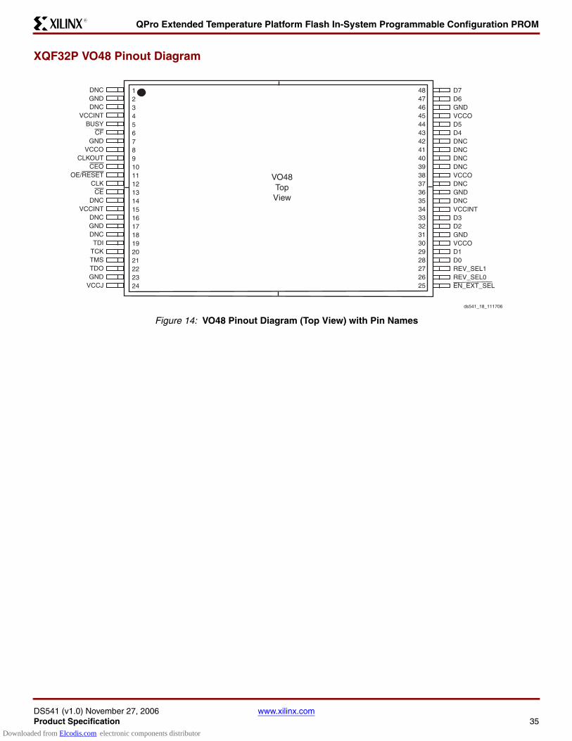
QPro Extended Temperature Platform Flash In-System Programmable Configuration PROM
DS541 (v1.0) November 27, 2006 www.xilinx.comProduct Specification 35
R
XQF32P VO48 Pinout Diagram
Figure 14: VO48 Pinout Diagram (Top View) with Pin Names
ds541_18_111706
123456789101112131415161718192021222324
484746454443424140393837363534333231302928272625
VO48TopView
DNCGNDDNC
VCCINTBUSY
CFGND
VCCOCLKOUT
CEOOE/RESET
CLKCE
DNCVCCINT
DNCGNDDNCTDI
TCKTMSTDOGND
D7D6GNDVCCOD5D4DNCDNCDNCDNCVCCODNCGNDDNCVCCINTD3D2GNDVCCOD1D0REV_SEL1REV_SEL0EN_EXT_SELVCCJ
Downloaded from Elcodis.com electronic components distributor
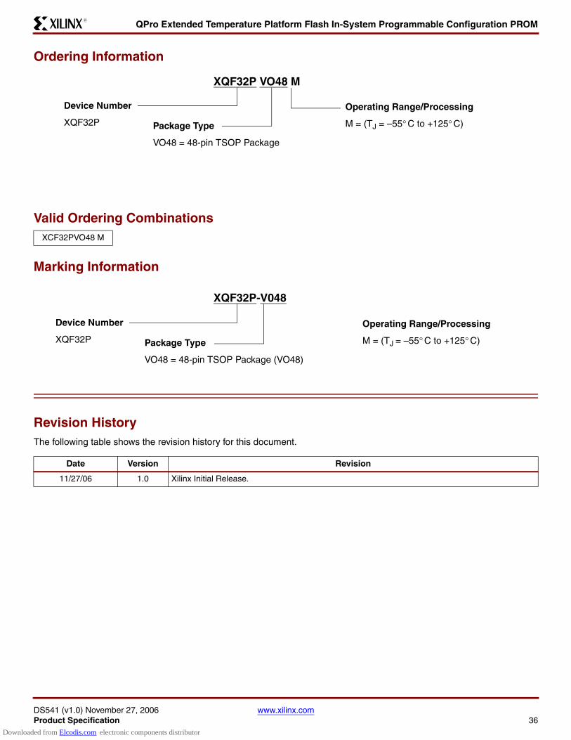
QPro Extended Temperature Platform Flash In-System Programmable Configuration PROM
DS541 (v1.0) November 27, 2006 www.xilinx.comProduct Specification 36
R
Ordering Information
Valid Ordering Combinations
Marking Information
Revision HistoryThe following table shows the revision history for this document.
XCF32PVO48 M
Date Version Revision
11/27/06 1.0 Xilinx Initial Release.
XQF32P VO48 M
Operating Range/Processing
M = (TJ = –55° C to +125° C)Package Type
VO48 = 48-pin TSOP Package
Device Number
XQF32P
XQF32P-V048
Operating Range/Processing
M = (TJ = –55° C to +125° C)Package Type
VO48 = 48-pin TSOP Package (VO48)
Device Number
XQF32P
Downloaded from Elcodis.com electronic components distributor