Embed Size (px)
Citation preview

Quadrature Down-converter for Wireless
Communications
by
Farsheed Mahmoudi
A thesis submitted in conformity with the requirements for the degree of Doctor of Philosophy
Edward S. Rogers Sr. Department of Electrical and Computer Engineering University of Toronto
Copyright by Farsheed Mahmoudi 2012

ii
Quadrature Down-converter for Wireless Communications Farsheed Mahmoudi
Doctor of Philosophy
Edward S. Rogers Sr. Department of Electrical and Computer Engineering
University of Toronto
2012
Abstract
Future generation of wireless systems will feature high data rates and be implemented in low
voltage CMOS technologies. Direct conversion receivers (DCRs) will be used in such systems
which will require low voltage RF front-ends with adequate linearity. The down-converter in a
DCR is a critical block in determining linearity. In addition to detailed DCR modeling in
MATLAB, this thesis, completed in 2005, deals with the design and characterization of a 1V,
8GHz quadrature down-converter. It consists of two mixers and a quadrature generator
implemented in a 0.18µm CMOS technology.
The mixer architecture proposed in this work uses a new trans-conductor. It simultaneously
satisfies the low voltage and high linearity requirements. It also relaxes the inherent trade-off
between gain and linearity governing CMOS active mixers. The implemented mixer occupies an
area of 320 x 400 µm2 and exhibits a power conversion gain of +6.5dB, a P-1dB of -5.5dBm, an
IIP3 of +3.5dBm, an IIP2 of better than +48dBm, a noise figure of 11.5dB, an LO to RF isolation
of 60dB at 8GHz and consumes 6.9mW of power from a 1V supply.
The proposed quadrature generator circuit features a new architecture which embeds the
quadrature generation scheme into the LO-buffer using active inductors. The circuit offers easy

iii
tune-ability for process, supply and temperature variations by relaxing the coupling between
amplitude and phase tuning of the outputs. The implemented circuit occupies an area of 150 x
90µm2 and exhibits an amplitude and quadrature phase accuracy of 1 dB and 1.5° respectively
over a bandwidth of 100 MHz with a power consumption of 12mW from a 1V supply including
the LO-buffer.
The quadrature down-converter features an image rejection ratio of better than 40 dB and
satisfies the potential target specifications of future mobile phones, extracted in this work.

iv
Acknowledgments
I would like to express my sincere gratitude to Professors C.A.T. Salama, W.T. Ng and
Willy Wong for their insightful guidance, patience, support and invaluable assistance throughout
the course of this work.
A special word of appreciation goes to my parents, and my brothers who have been a
constant source of support and encouragement.
I would also like to thank Professors Gulak and Sheikholeslami for their technical advice
and help.
My sincere thanks to Jaro Pristupa for his assistance. My appreciation extends to all the staff
and students in the Microelectronic Research Laboratory including Anthoula Kampouris, Dana
Reem, Richard Barber, Li Zhang Hou, Namdar Saniei, Farhang Vessal, Mohammad Kawokgy,
Mehrdad Ramezani, Behnam Mohammadi, Shahla Honarkhah, Alan Poon, Vincent Law,
Sotoudeh Hamedi-Hagh, Sameh Nassif, Dr. Park and Mr. Hou.
I would like to thank my friends, Maziar Esmaeili Khatir, Shahriar Shahramian and Ricardo
Aroca who kept me company with their constructive discussions and cheerful chats, and the rest
of my friends whose names are missing due to space limitation.
I would like to thank Prof. Shahriar Mirabbasi for serving as the external examiner of this
thesis.
Last but not least, I would like to thank my wife for her patience and support.
This work was supported by NSERC, Micronet, Gennum, Nortel Networks, PMC-Sierra,
Zarlink and CMC.
v
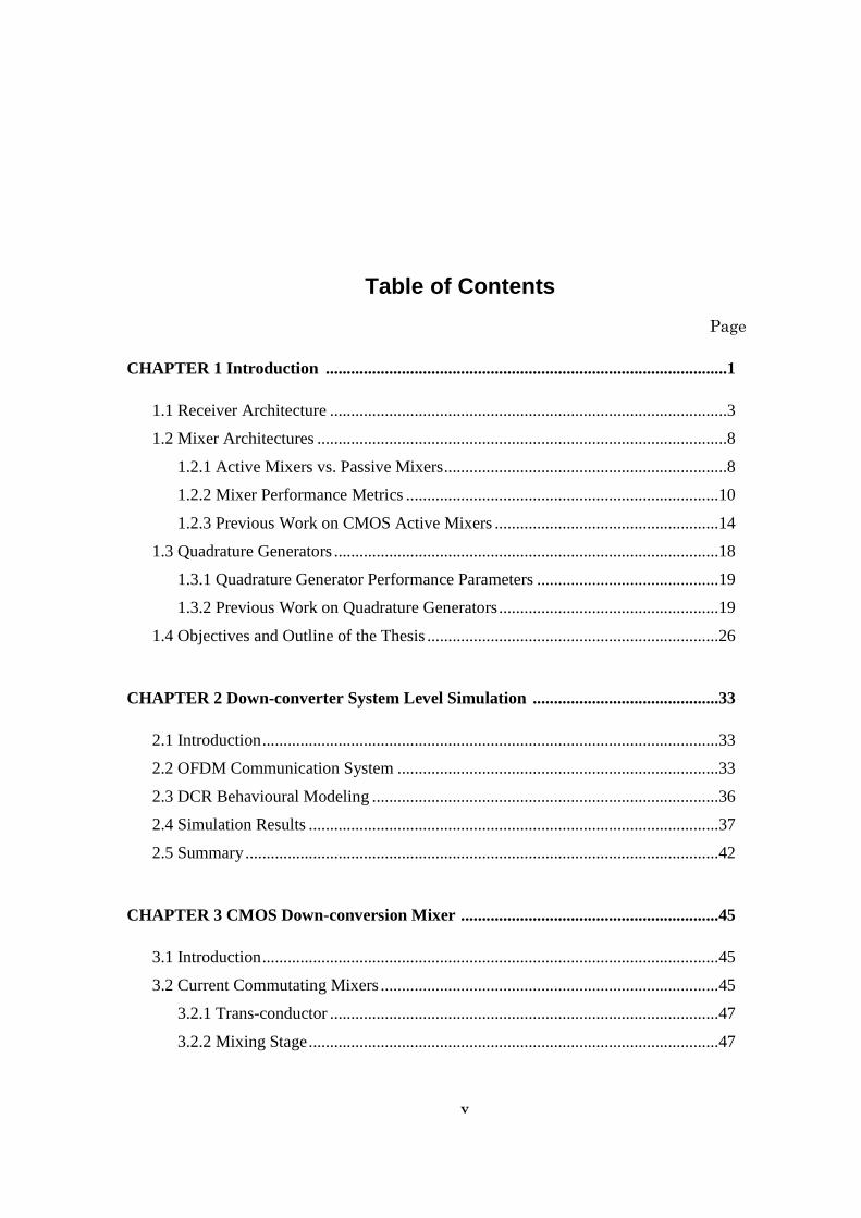
Table of Contents
Page
CHAPTER 1 Introduction ...............................................................................................1
1.1 Receiver Architecture ..............................................................................................3
1.2 Mixer Architectures .................................................................................................8
1.2.1 Active Mixers vs. Passive Mixers ...................................................................8
1.2.2 Mixer Performance Metrics ..........................................................................10
1.2.3 Previous Work on CMOS Active Mixers .....................................................14
1.3 Quadrature Generators ...........................................................................................18
1.3.1 Quadrature Generator Performance Parameters ...........................................19
1.3.2 Previous Work on Quadrature Generators ....................................................19
1.4 Objectives and Outline of the Thesis .....................................................................26
CHAPTER 2 Down-converter System Level Simulation ............................................33
2.1 Introduction ............................................................................................................33
2.2 OFDM Communication System ............................................................................33
2.3 DCR Behavioural Modeling ..................................................................................36
2.4 Simulation Results .................................................................................................37
2.5 Summary ................................................................................................................42
CHAPTER 3 CMOS Down-conversion Mixer .............................................................45
3.1 Introduction ............................................................................................................45
3.2 Current Commutating Mixers ................................................................................45
3.2.1 Trans-conductor ............................................................................................47
3.2.2 Mixing Stage .................................................................................................47

vi
Page
3.2.3 Trans-resistance Stage ..................................................................................48
3.3 CCM Linearization Techniques .............................................................................48
3.3.1 Source Degeneration (SDE) ..........................................................................49
3.3.2 Dynamic Matching (DMA)...........................................................................49
3.3.3 Cross-coupled Trans-conductors (CCT) .......................................................50
3.3.4 Trans-conductor using a CMOS Pair (CMP) ................................................51
3.3.5 Class AB Trans-conductor (ABT) ................................................................52
3.3.6 Summary .......................................................................................................53
3.4 Low-Voltage, High Linearity Mixer Design Issues ...............................................54
3.4.1 Effect of the trans-resistance Stage on the Linearity of CCM ......................54
3.4.2 Effect of the Mixing Stage on the Linearity of the CCM .............................54
3.4.3 Effect of the Trans-conductor on the linearity of the CCM ..........................55
3.5 Proposed Mixer and Design Methodology ............................................................57
3.5.1 Background ...................................................................................................57
3.5.2 Novel Mixer Architecture .............................................................................58
3.6 Layout ....................................................................................................................64
3.6.1 High Frequency Layout Considerations .......................................................65
3.6.2 Layout Considerations for Best Linearity Performance ...............................65
3.6.3 Mixer Layout ................................................................................................66
3.7 Post Layout Simulation ..........................................................................................68
3.8 Summary ................................................................................................................72
CHAPTER 4 CMOS Quadrature Generator ...............................................................75
4.1 Introduction ............................................................................................................75
4.2 Conventional Quadrature Generator ......................................................................75
4.3 Novel Quadrature Generator Architecture .............................................................78
4.4 Design and Analysis of the Proposed Quadrature Generator ................................80
4.5 Layout of the Quadrature Generator ......................................................................86
4.6 Post Layout Simulations ........................................................................................87
4.7 Summary ................................................................................................................91

vii
Page
CHAPTER 5 Implementation and Experimental Results ...........................................93
5.1 Introduction ............................................................................................................93
5.2 Mixer Implementation and Characterization .........................................................93
5.3 Quadrature Generator Implementation and Characterization ..............................104
5.4 Quadrature Down-converter Implementation and Characterization ....................111
5.5 Summary ..............................................................................................................114
CHAPTER 6 Conclusion ...............................................................................................123
APPENDIX A Design Ported to TSMC CMOS 65nm Technology ..........................127
A.1 Introduction .........................................................................................................127
A.2 Summary .............................................................................................................130

viii
List of Tables
Page
Table 1.1: Mobile Phone Generations ................................................................................2
Table 1.2: Tentative Target Specifications for a Mixer and Quadrature Generator Potentially
Suitable for Future Mobile Phone Receivers ........................................................7
Table 1.3: A Comparison Between Generic Types of CMOS Mixers ...............................9
Table 1.4: State of the Art Implementation of Various Mixer Architectures ...................18
Table 1.5: State of the Art Quadrature Generators ...........................................................26
Table 2.1: Specifications of the OFDM System under Consideration ..............................35
Table 2.2: Assumed LNA Characteristics ........................................................................36
Table 2.3: Tentative Specifications of the Mixer and Quadrature Generator ....................42
Table 3.1: Target Specifications and Post Layout Simulations .........................................70
Table 3.2: Effect of Process Variations on the Performance of the Mixer ........................71
Table 3.3: Effect of Temperature Variation on the Performance of the Mixer... ..............71
Table 4.1: Comparison between Target Specification and Post Layout Simulation for the Quadra-
ture Generator ..................................................................................................90
Table 4.2: Effect of Process Variation on the Performance of the Quadrature Generator.90
Table 4.3: Effect of Temperature Variation on the Performance of the Proposed Quadrature Gen-
erator. ...............................................................................................................91
Table 5.1: Comparison of the Low Voltage Mixer of this Work with Other Low Voltage Mixers
using Different Architectures (up to 2005) ....................................................100
Table 5.2: Comparison of the Low Voltage Mixer of this Work with Other Low Voltage Mixers
using Different Architectures (2005 to 2011) ................................................101
Table 5.3: Comparing the Linearity Characteristics of the Proposed Mixer and the Conventional
CCM [7,52] ....................................................................................................102
ix
Page
Table 5.4: Comparison of the Proposed Quadrature Generator to Previous Work up to 2004
..........................................................................................................................................109
Table 5.5: Comparison of the Proposed Quadrature Generator to Previous Work up to 2011
..........................................................................................................................................110
Table 5.6: I/Q Amplitude and Quadrature Phase Error Obtained from the IRR Method and the
Time Domain Characterization ......................................................................113
Table 5.7: Quadrature Down-converter (QD) compared to other DCRs targeting similar applica-
tions. ...............................................................................................................113
Table A.1: Down-converter comparison..........................................................................128
Table A.2: Quadrature Down-converter port to 65nm technology ..................................129

x
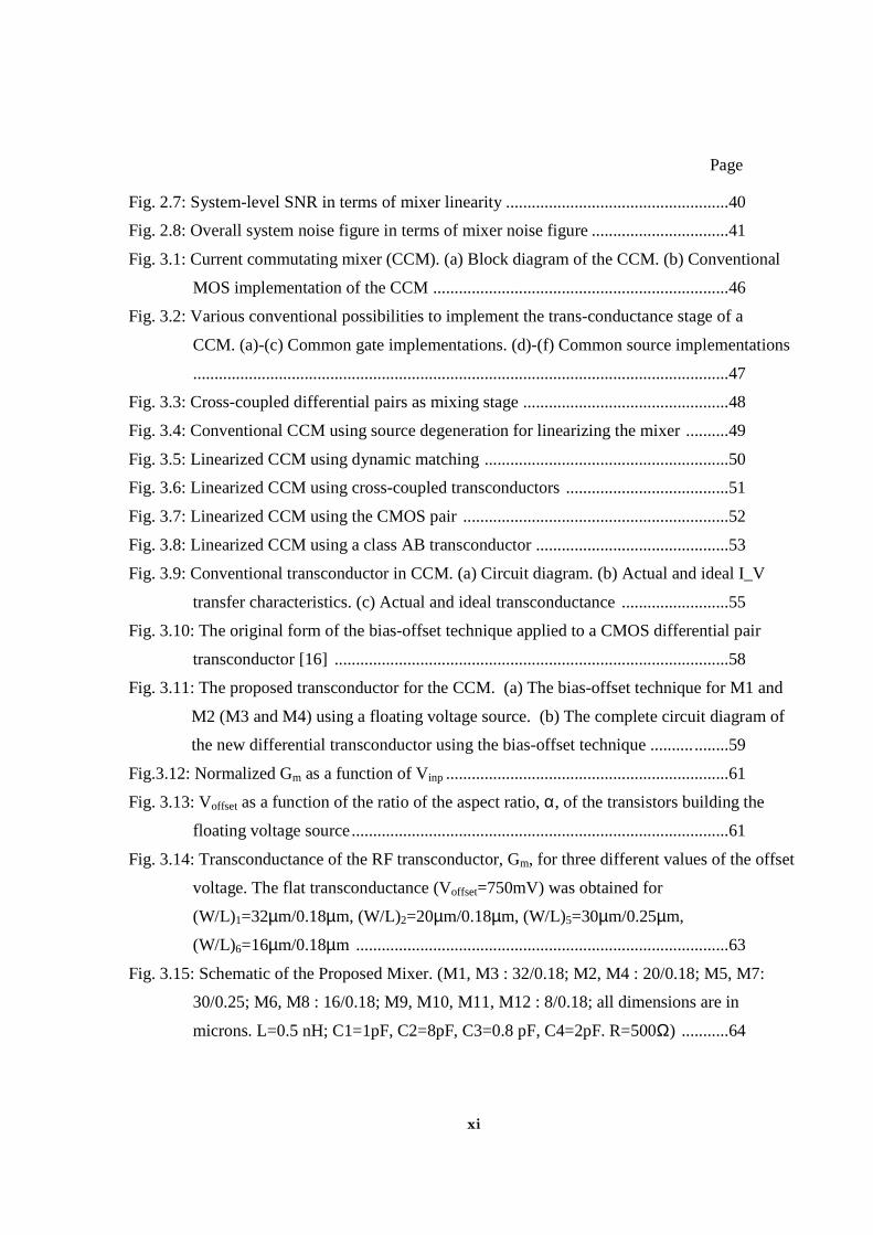
List of Figures
Page
Fig. 1.1: Effect of nonlinear RF front-end on the spectrum of the received signal .............2
Fig. 1.2: Typical architecture of a direct conversion receiver (DCR) ................................4
Fig. 1.3: The LO to RF leakage due to poor LO-RF port isolation ....................................5
Fig. 1.4: The effect of AC-coupling on WCDMA and OFDM communication systems ....5
Fig. 1.5: Current commutating mixer. (a) Block diagram. (b) Typical CMOS implementation
............................................................................................................................ 14
Fig. 1.6: Harmonic mixer ..................................................................................................15
Fig. 1.7: Dual gate mixer. (a) Block diagram. (b) Typical CMOS implementation ..........16
Fig. 1.8: Back gate mixer. (a) Block diagram. (b) Typical CMOS implementation .........17
Fig. 1.9: RC-CR filter used as quadrature generator. (a) Circuit diagram. (b) Phase of the transfer
function of the two outputs. (c) Magnitude of the transfer function of the two outputs .
............................................................................................................................20
Fig. 1.10: Single stage polyphase filter used as quadrature generator .............................21
Fig. 1.11: Haven’s technique for generating quadrature signals ......................................22
Fig. 1.12: Frequency division technique ...........................................................................23
Fig. 1.13: Ring oscillator quadrature generator ................................................................24
Fig. 1.14: I-Q signal generator architecture using CON ...................................................25
Fig. 1.15: Quadrature LC-oscillator ..................................................................................25
Fig. 2.1: Typical OFDM communication system. .............................................................34
Fig. 2.2: Typical direct conversion receiver block diagram. .............................................34
Fig. 2.3: OFDM modulator and demodulator block diagram. ...........................................35
Fig. 2.4: SNR vs. phase noise of the mixer LO CLK. .......................................................38
Fig. 2.5: Mixer LO phase noise mask meeting BER spec of 10-3. .....................................38
Fig. 2.6: Receiver BER versus quadrature phase error. .....................................................39
xi
Page
Fig. 2.7: System-level SNR in terms of mixer linearity ....................................................40
Fig. 2.8: Overall system noise figure in terms of mixer noise figure ................................41
Fig. 3.1: Current commutating mixer (CCM). (a) Block diagram of the CCM. (b) Conventional
MOS implementation of the CCM .....................................................................46
Fig. 3.2: Various conventional possibilities to implement the trans-conductance stage of a
CCM. (a)-(c) Common gate implementations. (d)-(f) Common source implementations
.............................................................................................................................47
Fig. 3.3: Cross-coupled differential pairs as mixing stage ................................................48
Fig. 3.4: Conventional CCM using source degeneration for linearizing the mixer ..........49
Fig. 3.5: Linearized CCM using dynamic matching .........................................................50
Fig. 3.6: Linearized CCM using cross-coupled transconductors ......................................51
Fig. 3.7: Linearized CCM using the CMOS pair ..............................................................52
Fig. 3.8: Linearized CCM using a class AB transconductor .............................................53
Fig. 3.9: Conventional transconductor in CCM. (a) Circuit diagram. (b) Actual and ideal I_V
transfer characteristics. (c) Actual and ideal transconductance .........................55
Fig. 3.10: The original form of the bias-offset technique applied to a CMOS differential pair
transconductor [16] ............................................................................................58
Fig. 3.11: The proposed transconductor for the CCM. (a) The bias-offset technique for M1 and
M2 (M3 and M4) using a floating voltage source. (b) The complete circuit diagram of
the new differential transconductor using the bias-offset technique .......... ........59
Fig.3.12: Normalized Gm as a function of Vinp ..................................................................61
Fig. 3.13: Voffset as a function of the ratio of the aspect ratio, α, of the transistors building the
floating voltage source ........................................................................................61
Fig. 3.14: Transconductance of the RF transconductor, Gm, for three different values of the offset
voltage. The flat transconductance (Voffset=750mV) was obtained for
(W/L)1=32µm/0.18µm, (W/L)2=20µm/0.18µm, (W/L)5=30µm/0.25µm,
(W/L)6=16µm/0.18µm .......................................................................................63
Fig. 3.15: Schematic of the Proposed Mixer. (M1, M3 : 32/0.18; M2, M4 : 20/0.18; M5, M7:
30/0.25; M6, M8 : 16/0.18; M9, M10, M11, M12 : 8/0.18; all dimensions are in
microns. L=0.5 nH; C1=1pF, C2=8pF, C3=0.8 pF, C4=2pF. R=500Ω) ...........64

xii
Page
Fig. 3.16: Layout consideration to achieve best linearity performance ............................66
Fig. 3.17: Layout of the proposed mixer ...........................................................................67
Fig. 3.18: Layout of the integrated spiral inductor designed using the ADS software.... ..67
Fig. 3.19: (a) Spiral integrated inductor. (b) Lumped model at 8 GHz for post layout simulation
.............................................................................................................................68
Fig. 3.20: Two-tone simulation revealing an IIP3 of +2 dBm ..........................................69
Fig. 3.21: Power transfer characteristics of the mixer illustrating a simulated P-1dB of -10 dBm
and a PCG of +12 dB .........................................................................................69
Fig. 4.1: Quadrature generation components embedded in the LO buffer .......................76
Fig. 4.2: Block diagram of the quadrature generator under consideration ........................78
Fig. 4.3: Differential active inductor implementation based on the Gm-C architecture. ....79
Fig. 4.4: Common-mode stabilizer circuit ........................................................................80
Fig. 4.5: Small signal model of the MOST in the active region of operation ...................80
Fig. 4.6: Circuit of the quadrature generator. (M1 to M8 : 10/0.18; M21, M22, M24 and M25:
9/0.18; M13, M14, M19 and M20 : 12/0.18; M9 to M12 : 5/0.18; M15 to M18 : 12/0.18; M23
and M26 are zero threshold voltage devices : 6/0.5; all dimensions are in µm. Vdd=1V,
VB=750mV, VB1=150mV, VB2=0, VC=850mV ..................................................81
Fig. 4.7: Equivalent common mode half circuit of the quadrature generator ...................84
Fig. 4.8: Post-layout simulation characteristics of the quadrature generator. (a) The magnitude
and phase of the transfer function of the four outputs. (b) The time domain quadrature
outputs .................................................................................................................88
Fig. 4.9: Simulation results of the quadrature generator over the bandwidth of interest. (a) The
phase of the transfer function of the outputs. (b) The amplitudes of the quadrature
outputs .................................................................................................................89
Fig. 5.1: Micrograph of the mixer ......................................................................................94
Fig. 5.2: Conversion gain and 1-dB compression point measurement setup ....................95
Fig. 5.3: Power transfer characteristics of the mixer illustrating a measured 1-dB compression
point of -5.5dBm and a power conversion gain (PCG) of +6.5 dB ....................96
Fig. 5.4: Two-tone test measurement setup .......................................................................96
Fig. 5.5: Two-tone test revealing a measured IIP3 of +3.5 dBm versus a simulated IIP3 of +2
dBm .....................................................................................................................97

xiii
Page
Fig. 5.6: Noise figure measurement setup .........................................................................98
Fig. 5.7: RF port to LO port isolation measurement setup ................................................99
Fig. 5.8: CMOS mixers published in the literature [14-59]. Input referred third order intercept
point versus noise .............................................................................................................103
Fig. 5.9: Proposed CMOS mixer compared to state of the art published work [14-59]. The
vertical axis represents linearity over power in decibels .................................................104
Fig. 5.10: Micrograph of the quadrature generator .........................................................105
Fig. 5.11: Quadrature accuracy measurement setup ........................................................105
Fig. 5.12: Comparison between measurement and simulation results. (a) Quadrature phase. (b)
Magnitude of the transfer function of the outputs ............................................106
Fig. 5.13: The time domain measured output of the quadrature generator ......................107
Fig. 5.14: Phase noise measurement setup .......................................................................107
Fig. 5.15: Measured phase noise of the quadrature generator .........................................108
Fig. 5.16: Quadrature generator comparison to previous work [60-81] ..........................110
Fig. 5.17: Micrograph of the fabricated quadrature downconverter ...............................111
Fig. 5.18: Image rejection ratio measurement setup ........................................................112
Fig. 5.19: Image rejection ratio measurement results over a bandwidth of 100 MHz.....112
Fig. A.1: CMOS technology threshold voltage and supply voltage scaling ....................128

xiv
List of Appendices
Page
Appendix A: Design Ported to 65nm CMOS Technology .............................................127
xv
Glossary
ABT: Class AB Trans-conductor
ADC: Analog to Digital Converter
ADS: Advanced Design System
AGC: Automatic Gain Control
BAW: Bulk Acoustic Wave
BER: Bit Error Ratio
BGM: Back Gate Mixer
BPF: Band-Pass Filter
CCM: Current Commutating Mixer
CCT: Cross-Coupled Trans-conductor
CDMA: Code Division Multiple Access
CLK: Clock
CMP: Complementary Metal Oxide Semiconductor Pair
CON: Cellular Oscillator Network
DCR: Direct Conversion Receiver
DGM: Dual Gate Mixer
DMA: Dynamic Matching
DSB: Double Side Band
DUT: Device Under Test
FD: Frequency Division
FDMA: Frequency Division Multiple Access
FFT: Fast Fourier Transform
HAM: Harmonic Mixer
HBT: Hetero-junction Bipolar Transistors
IF: Intermediate Frequency

xvi
IFFT: Inverse Fast Fourier Transform
I/Q: In-phase/Quadrature
IIP2: 2nd Order Input Referred Intercept Point
IIP3: 3rd Order Input Referred Intercept Point
IRR: Image Rejection Ratio
ISI: Inter-Symbol Interference
LCQ: LC Quadrature Oscillator
LNA: Low Noise Amplifier
LO: Local Oscillator
LPF: Low-Pass Filter
LPTV: Linear Periodic Time Varying
MMT: Manual Microwave Tuners
MOST: Metal Oxide Semiconductor Transistor
NF: Noise Figure
NL: Non-Linear
OFDM: Orthogonal Frequency Division Multiplexing
PCG: Power Conversion Gain
PPF: Poly-Phase Filter
QD: Quadrature Down-converter
QG: Quadrature Generator
RCF: RC-CR Filter
RF: Radio Frequency
RO: Ring Oscillator
SAA: Subtraction and Addition
SDE: Source Degeneration
SGS: Signal Ground Signal
SNR: Signal to Noise Ratio
SOLT: Short Open Load Through
SSB: Single Side Band
TDMA: Time Division Multiple Access

xvii
VCO: Voltage Controlled Oscillator
VGA: Variable Gain Amplifier
WCDMA: Wide-band Code Division Multiple Access
WLAN: Wireless Local Area Network

Chapter 1 - Introduction
1
CHAPTER 1
CHAPTER 1: Introduction
It is generally expected that the number of portable handsets will exceed the number of personal
computers (PC) connected to the internet with the deployment of the next generation of mobile
phones [1]. The first steps toward this have been taken at the system level to support advanced
and wideband multimedia services, which makes low voltage, low power CMOS receivers sup-
porting these systems highly desirable.
Table 1.1 compares some of the tentative specifications of the future mobile phone system (as
reported in the literature) to its previous generations. The specifications listed in the table, direct-
ly affect the circuit level implementation of radio frequency (RF) receiver front-ends. The future
generation of mobile phones is expected to use a data rate of 100 Mbps or more [2]. Depending
on the modulation and multiple access scheme applied, this data rate may translate into a band-
width of 50 MHz or more. This relatively wide bandwidth causes the issue of linearity to become
one of the major concerns in the design of RF receiver front ends. Fig. 1.1 is a simple illustration
of the way nonlinear RF front-end degrades the performance of the receiver through in-band in-
termodulation products. Increasing the bandwidth of the RF/IF front-end degrades the linearity
characteristics of these circuitry due to increased intermodulation products hitting each desired
channel. In addition to intermodulation products, the two horizontal shaded portions of the spec-
trum show the scaled convolution of the incoming spectrum, causing a widening of the spectrum
due to second and third order non-linearities which in turn degrades the quality of the received
signal.

Chapter 1 - Introduction
2
As mentioned in Table 1.1, orthogonal frequency-division multiplexing (OFDM) is a strong can-
didate for the multiplexing scheme used in future mobile systems [3-5].
Table 1.1 Mobile Phone Generations
Characteristics 1G 2G 3G Future Mobile
Systems*
Spectrum 900MHz 1800MHz 2GHz 2-8GHz
Multiplexing Analog FDMA TDMA CDMA OFDM
Targeted data rate N/A 14.4kbits/sec 2Mbits/sec >100Mbits/sec
Real data rate 2.4kbits/sec 9.6kbits/sec 384kbits/sec **
Bandwidth 30 kHz 200 kHz 5-20 MHz 50-100 MHz
Modulation FM GMSK QPSK 64QAM
Time frame 1980-1994 1995-2001 2002-2005 > 2010
* These are tentative system level specifications, obtained from the available literature.
** The data rate associated with these mobile systems varies for different conditions. For instance, vehicular
data rate versus static data rate.
Fig.1.1 Effect of nonlinear RF front-end on the spectrum of the received signal.

Chapter 1 - Introduction
3
The analog and digital front end of a mobile phone is usually partitioned based on technology
usage. This allows a flexible choice of technologies which typically results in the use of BIC-
MOS for RF and analog, mainly because of the superior RF performance of hetero-junction bi-
polar transistors (HBT) over metal oxide semiconductor transistors (MOST)[6], and CMOS for
the digital signal processing due to the high level of achievable integration. If the whole receiver
is to be implemented on a single chip, the partitioning of the chip is no longer based on the tech-
nology, but rather on the required functionality. This obviously requires the integration of the
analog and digital signal processing sections on the same chip. Since the Digital section of the
whole system uses CMOS, it is likely that the analog front end will also be implemented in
CMOS [7]. In this work, a standard CMOS 0.18 µm technology is chosen to implement the RF
circuitry under consideration using a 1V power supply1. Such a low voltage supply allows for
easy migration of the RF circuits, designed in this work, to more advanced CMOS technologies
which will be used in the digital section of the chip to achieve superior functionality2.
1.1 Receiver Architecture
Among various RF wireless receiver architectures reported in the literature [8-12], the direct
conversion receiver (DCR), illustrated in Fig. 1.2, is considered as the most likely architecture to
be used in the future generation of mobile phones3. The DCR offers a simple architecture which
allows a low power, fully monolithic implementation of the RF front end [13]. That front-end
consists of three main blocks, namely an RF filter to eliminate the undesired frequency content
of the signal and to select the channel of interest, a low-noise amplifier (LNA), and a quadrature
down-converter to demodulate the incoming angle-modulated data. The main issues involved in
1 The nominal power supply for standard devices in a CMOS 0.18 µm technology is 1.8V. 2 The proposed design in this work is ported to 65nm CMOS to prove the portability of the design to more ad-
vanced, lower supply voltage CMOS technologies. See Appendix A. 3 Currently, most mobile handsets use DCR. Base station receivers are also migrating to DCR to ease the de-sign of down-converter and base-band circuitry.

Chapter 1 - Introduction
4
the design of a DCR include the DC-offset, even and odd order intermodulation terms, flicker
noise and the gain and phase mismatches between the in-phase and quadrature paths [14,15].
These issues are briefly discussed in the following paragraphs.
Fig.1.2 Typical architecture of a direct conversion receiver (DCR).
In addition to DC-offset present in integrated circuits due to device mismatches, the DC-offset
becomes a more pronounced concern in DCRs because the LO signal applied to the mixer is at
the same frequency as the RF carrier. The leakage of the LO signal to the RF port of the mixers,
as shown in Fig. 1.3, results in an undesired self-down-conversion of the LO signal to DC. This
leakage appears at the output of the RF front end in the form of a DC-offset and falls within the
bandwidth of interest. In order to overcome this problem, a number of solutions have been re-
ported in the literature [16,17]. Most of these approaches add to the area, power consumption and
complexity of the design and may not be acceptable.
The simplest option which does not add to the complexity of the design, is to AC-couple the out-
put of the mixer to the low-pass filter [14], within the DCR. The feasibility of this approach de-
pends on the multiplexing scheme and the bandwidth of the received signal [17,18]. As men-
tioned previously, OFDM is a possibility for the multiplexing scheme of future mobile systems.
The feasibility of AC-coupling for other types of multiple access schemes such as WCDMA has
already been investigated in the literature. As illustrated in Fig. 1.4, applying AC-coupling to

Chapter 1 - Introduction
5
WCDMA, suppresses the DC-offset along with part of the desired spectrum. In the case of
OFDM, if no data is assigned to the baseband subcarrier located at DC, as implemented in the
OFDM IEEE 802.11a wireless local area network (WLAN) standard [19], AC-coupling does not
affect the information bearing portion of the spectrum, as shown in Fig. 1.4. In this work, OFDM
is assumed as the multiple access scheme, due to its obvious advantages over WCDMA in view
of DCRs [4].
Fig.1.3 The LO to RF leakage due to poor LO to RF isolation.
Fig.1.4 Implication of AC-coupled receivers on WCDMA and OFDM communication systems.

Chapter 1 - Introduction
6
In a direct conversion receiver, even order intermodulation terms resulting from out of band
blockers fall in the bandwidth of the incoming signal after down conversion. For this reason, the
second order nonlinearity of the down converter should be set such that it meets the requirement
of the targeted application. Depending on frequency planning and amount of out-of-band rejec-
tion provided by the RF filter, the significance of even order intermodulation products varies.
Bautista et al. [20], introduced a novel way of reducing second order intermodulation products
by adding a considerable amount of circuit overhead to the core of the design.
The issue of flicker noise in DCRs arises from the fact that most of the noise power is concen-
trated in the same region of the spectrum as the desired signal. In the case considered in this
work, simple AC-coupling can be used to mitigate this issue as described above.
The gain and phase mismatch between the in-phase and quadrature paths in a DCR degrades the
quality of the received signal. The mismatch is partly attributed to the unbalance between the two
mixers involved in the receive path and partly due to imperfections in the quadrature generator.
These mismatches affect the image rejection ratio (IRR) defined as the down-converter’s ability
to reject signals at its image frequency. IRR is normally expressed as the ratio of the image sig-
nal to the desired signal in dB at the output of the down-converter.
The linearity characteristics of the RF front-end of a DCR are to a great extent determined by the
linearity of the mixer. This is because the RF signal captured by the antenna reaches the mixers
after one or possibly two steps of amplification by the one or two LNAs. This imposes stringent
requirements on the dynamic range of the mixers which play an important role in determining
the linearity of the RF front-end [21].
The goal of this thesis is to devise a new architecture and design methodology for low voltage,
low power CMOS RF down conversion mixers, and quadrature generators with adequate lineari-
ty, amplitude matching and quadrature phase accuracy for direct conversion receivers operating

Chapter 1 - Introduction
7
at 8 GHz [2]. The quadrature down-converter (the combination of the mixer and the quadrature
generator) is intended to satisfy the tentative target specifications listed in Table 1.21.
Table 1.2 Tentative Target Specifications for a Mixer and Quadrature Generator Potentially Suitable for Future Mobile Phone Receivers.
Circuit Parameter Value
Mixer
Supply Voltage** 1 V
RF & LO frequency** 8 GHz
Conversion Gain** > 6 dB
IIP2** > 50 dB
IIP3 > 3dB
P-1dB > -7dBm
LO-RF Isolation** > 50 dB
Noise Figure <13 dB
Power Consumption and Area
Minimum
Quadrature generator
Supply Voltage** 1 V
I/Q phase mismatch <2°
Power Consumption and Area
Minimum
Phase noise at 1MHz offset -110dBc/Hz
Quadrature Downconvert-
er
Image Rejection Ratio
(IRR)
> 40 dB
** These values are set as target to stay competitive with the state of the art design. The rest of the targets are obtained from system-level simulation in MATLAB. See Chapter 2 and the MATLAB codes available at: http://www.vrg.utoronto.ca/~ngwt/Resources/MATLAB/DCR.
1The tentative target specifications of the design were generated through system level simulations using MATLAB, as discussed in Chapter 2.

Chapter 1 - Introduction
8
1.2 Mixer Architectures
Mixers are used to translate the frequency of the incoming RF signal to the intermediate frequen-
cy (IF) of interest, which is zero in the case of a DCR. Frequency translation is typically per-
formed by multiplying the incoming RF signal by the local oscillator (LO) signal in the time do-
main. The multiplication of the RF signal and the LO signal is typically done by exploiting the
nonlinear (NL) characteristics of a circuit or by using the LO signal to convert a linear time in-
variant circuit to a linear periodically time variant (LPTV) one [22].
1.2.1 Active Mixers Vs. Passive Mixers
Mixers can be classified as active or passive depending on whether or not they provide power
gain at the input radio frequency. They can use an unbalanced, single balanced or double bal-
anced architecture. The typical properties of each of these generic mixers are listed in Table 1.3.
In a DCR, the only opportunity for amplifying the received RF signal is through the LNA and
one step of down-conversion. Therefore, the RF front end gain is relatively low by comparison to
most other types of receivers. This issue degrades the noise characteristics and hence the sensi-
tivity of the receiver which is a measure of how well the receiver captures weak signals. Since
active mixers typically result in better sensitivity, in this work they are preferred over passive
ones despite the very good linearity performance of the latter.

Chapter 1 - Introduction
9
Table 1.3 A Comparison Between Generic Types of CMOS Mixers
Passive Active
Un-Balanced
Single Balanced
Double Balanced
Un-Balanced
Single Balanced
Double Balanced
Conversion gain
<1
>1, desirable for better noise performance and sensitivity
Linearity Excellent Relatively poor, can be improved by circuit
techniques
Noise
figure (NF)
Depending on the devices used as switches, can have relatively poor noise performance, due to
the inherent conversion loss.
Relatively good, depending on the amount of conversion gain, and whether noise optimization
is done on the transistors individually.
Even order nonlinearity
Good Good Ideally None Poor good Ideally None
Compression point
Relatively good Relatively poor, due to the saturation effect of active devices
Bandwidth Relatively wide bandwidth. Limited by switch
parasitic capacitance Relatively narrow band
Spurious tone(s)
LO, RF, relatively
weak nωLO-mωRF*
and
kωLO-ωRF**
LO, RF and relatively
weak
nωLO-mωRF
and
kωLO-ωRF
relatively weak
nωLO-mωRF
and
kωLO-ωRF
LO, RF and relatively
strong
nωLO-mωRF
LO, RF and relatively
strong
nωLO-mωRF
Relatively strong
nωLO-mωRF
DC current Zero Significant
* These spurs are caused by ‘m+n’ order non-linearities.
** k=3,5,7,… in case of square LO signal.

Chapter 1 - Introduction
10
1.2.2 Mixer Performance Metrics
The critical performance metrics for a mixer employed in a DCR intended for relatively wide-
band portable applications are: its third order and second order nonlinearities, RF-port to LO-port
isolation, noise figure at baseband frequencies, LO-power required for driving the mixer LO
port, conversion gain and 1-dB compression point. These metrics are discussed briefly in the fol-
lowing paragraphs.
A mixer can be described by the following nonlinear relation between the input signal x and the
output signal y y F x( )= (1.1)
Assuming weakly nonlinear behaviour, using Taylor expansion of (1.1) and omitting the signal
independent term for the sake of simplification (without loss of generality), y can be expressed as
y b1x b
2x2
b3x3 …+ + += (1.2)
Defining the input signal x as the sum of two cosines of equal amplitudes at angular frequencies
ω1 and ω2, given by
x A ω1t A ω2tcos+cos= (1.3)
then y is given by
y b1A ω1t b1A ω
2tcos+cos b2
1
2---A
2 ω1 ω2–( )tcos+=
b+ 33
4---A
32ω1 ω2–( )tcos b3+ 3
4---A3
2ω2 ω1–( )tcos …+ (1.4)

Chapter 1 - Introduction
11
Because of the third order nonlinearity x3, and second order nonlinearity x2 terms, the output will
contain undesired tones located at angular frequencies 2ω1-ω2, 2ω2-ω1 and |ω1-ω2| respectively
as shown in equation (1.4). These spurious tones are usually considered because they likely fall
in the frequency band of interest (i.e. the signal band); and degrade the bit-error-rate (BER) of
the received signal.
• Third Order Intercept Point
The third order input intercept point (IIP3) is a measure of the third order nonlinearity of the
mixer and is defined as the magnitude of the input signal (xIIP3) for which the third order inter-
modulation term at the output has the same magnitude as the first order term. XIIP3 is derived
from (1.4) and is given by
xIIP34
3---b1
b3------= (1.5)
• Second Order Intercept Point
The second order input intercept point (IIP2) is defined as the magnitude of the input signal
(xIIP2) for which the second order intermodulation term at the output has the same magnitude as
the linear (first order) term. This definition results in
xIIP2 2b1
b2------= (1.6)
• Power Conversion Gain
The power conversion gain of a mixer is the ratio of the power delivered to the load at the IF
when the power of all out of band components is excluded, over the available power of the
source. The power conversion gain is usually expressed in Decibels (dB). Appropriate conver-

Chapter 1 - Introduction
12
sion gain of the mixer, helps to decrease the effect of the noise generated by subsequent stages,
and hence improves the noise performance of the RF front end. Increasing the conversion gain
too much, may impose stringent requirement on the dynamic range of the following stage.
• 1-dB Compression Point
In a weakly nonlinear system, the third order nonlinearity of mixers generates a term at the same
frequency as the output first order term which contributes to the gain of the mixer. This phenom-
enon can be explained based on the following trigonometric identity given that x=cosωt
x3 ωtcos( )=
3 1
4--- 3ωt 3
4--- ω tcos+cos= (1.7)
As observed, the second term on the right-hand side of (1.7) affects the linear gain of the mixer.
From (1.2) and (1.7) it can be seen that the effective gain of the mixer due to both the linear term
and third order nonlinearity is given by
Effective g– ain b1=3
4---b3A
2+ (1.8)
Depending on the sign of b3, the third order nonlinearity may result in either an increase or de-
crease of the mixer gain. In most practical cases, this phenomenon results in the reduction of the
gain which results in the definition of the 1-dB compression point as the magnitude of the input
signal for which the gain drops by 1 dB.
• Port-to-Port Isolation
The port-to-port isolation of the mixer is defined as the ratio (in dB) of the power level applied at
one port of the mixer to the resulting power level at the same frequency at the other port. In the
case of a direct conversion receiver, as illustrated in Fig. 1.3, poor RF port to LO port isolation
results in a DC-offset which may saturate the stage following the mixer.

Chapter 1 - Introduction
13
• Noise
The mixer noise is a concern because it can mask a weak desired signal. It is characterized by the
noise figure (NF) as a metric of the degradation of the signal to noise ratio (SNR) while the sig-
nal passes through the mixer, and is defined as
NF =SNR at the input, in the input signal band
SNR at the output, in the output signal band (1.9)
If the signal band is very narrow, the conversion gain and noise power spectral density in the in-
put and output signal bands are almost flat, in this case
N F
S i
N i
-----
S o
N o
------ ------------
S i
S o
-----N o
N i
------⋅ 1A----
N o
N i
------⋅= = = =Total output noise
Output noise due to the input noise in the input frequency band
(1.10)
where Si, So, Ni, No and A are the input signal power per unit bandwidth, output signal power per
unit bandwidth, input noise power per unit bandwidth, output noise power per unit bandwidth
and power gain of the mixer, respectively. In DCRs the image band is part of the input signal
band and contributes to the denominator of (1.10); in this case, the NF is called double-sideband
(DSB) as opposed to the single-sideband (SSB) NF in heterodyne receivers where the image
band is not part of the input signal and therefore does not contribute to the denominator of (1.10).
The DSB NF is typically 3 dB lower than the SSB NF.
• LO Power
The amount of power applied to the LO port of the mixer is often a concern and must be mini-
mized. This issue is of particular concern in low voltage designs.
Chapter 1 - Introduction
14
1.2.3 Previous Work on CMOS Active Mixers
CMOS active mixers reported to date, fall within one of the following categories: Current Com-
mutating Mixers (CCM) [23], Harmonic Mixers (HAM) [24], Dual Gate Mixers (DGM) [25] and
Back Gate Mixers (BGM)[26]. In what follows, the various CMOS active mixer architectures
and associated design issues are briefly discussed.
• Current Commutating Mixers (CCM) [23]
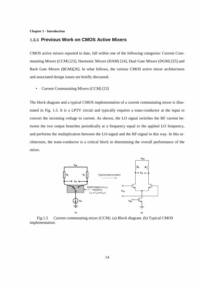
The block diagram and a typical CMOS implementation of a current commutating mixer is illus-
trated in Fig. 1.5. It is a LPTV circuit and typically requires a trans-conductor at the input to
convert the incoming voltage to current. As shown, the LO signal switches the RF current be-
tween the two output branches periodically at a frequency equal to the applied LO frequency,
and performs the multiplication between the LO-signal and the RF-signal in this way. In this ar-
chitecture, the trans-conductor is a critical block in determining the overall performance of the
mixer.
Fig.1.5 Current commutating mixer (CCM). (a) Block diagram. (b) Typical CMOS
implementation.

Chapter 1 - Introduction
15
• Harmonic Mixers (HAM) [24]
The harmonic mixer is a variant of the CCM and therefore a LPTV circuit. It allows for the use
of a local oscillator at a fraction of the LO frequency of a CCM. An example of an even harmon-
ic mixer is illustrated in Fig. 1.6. The main drawback associated with this architecture is the de-
pendence on a four-phase local oscillator with precise quadrature phase and 50% duty cycle
which adds to the complexity and power consumption of the design.
Fig.1.6 Harmonic mixer.
• Dual Gate Mixers (DGM) [25]
Dual gate transistors have been traditionally used as mixers in GaAs technology. They can also
be implemented in CMOS technology. Fig. 1.7 illustrates the block diagram of a dual gate mixer
showing its principle of operation. In this scheme, the local oscillator, modulates the transcon-
ductance of the RF transistor at a frequency equal to the LO frequency and hereby introduces the

Chapter 1 - Introduction
16
concept of periodically time variance. Therefore the dual-gate mixer is also a LPTV circuit. The
circuit architecture of a DGM typically consists of at least two stacked transistors. Because of
this feature the DGM is unsuitable for low-voltage applications.
Fig.1.7 Dual gate mixer. (a) Block diagram. (b) Typical CMOS implementation.
• Back-Gate Mixer (BGM) [26]
Fig. 1.8 shows the principle of operation of a back gate mixer. In this architecture the LO signal
varies the threshold voltage of the transistor at a frequency equal to the frequency of the LO,
therefore the BGM is also a LPTV circuit. In this circuit, since the LO signal is applied to the
bulk of the MOST, it may inject a considerable amount of noise to the substrate which is highly
undesirable for GHz applications. Therefore, the application of this architecture is practically
limited to twin-tub technologies or technologies where the deep N-well is an option. The isola-
tion between the LO port and all the other ports of this type of mixer is poor because of the para-
sitic capacitance between the terminals of the MOST and its bulk.

Chapter 1 - Introduction
17
Fig.1.8 Back gate mixer. (a) Block diagram. (b) Typical CMOS implementation.
• Summary of Previous Mixer Work
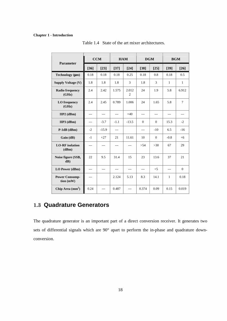
The state of the art implementation of each of the above mentioned active mixer topologies in
various CMOS technologies are summarized in Table 1.4. From the Table, and the previous brief
discussion on the mixer architectures, it is evident that none of the previously reported architec-
tures provides an efficient solution to meet the good linearity, low voltage operation and design
simplicity requirements of the future generation of mobile phones.
Chapter 1 - Introduction
18
Table 1.4 State of the art mixer architectures.
Parameter CCM HAM DGM BGM
[36] [23] [37] [24] [38] [25] [39] [26]
Technology (µµµµm) 0.18 0.18 0.18 0.25 0.18 0.8 0.18 0.5
Supply Voltage (V) 1.8 1.8 1.8 3 1.8 3 1 1
Radio frequency (GHz)
2.4 2.42 1.575 2.0122
24 1.9 5.8 6.912
LO frequency (GHz)
2.4 2.45 0.789 1.006 24 1.65 5.8 7
IIP2 (dBm) --- --- --- +40 --- --- --- ---
IIP3 (dBm) --- -3.7 -1.1 -13.5 0 0 15.3 -2
P-1dB (dBm) -2 -15.9 --- --- -10 6.5 -16
Gain (dB) -1 +27 21 11.61 10 0 -0.8 +6
LO-RF isolation (dBm)
--- --- --- --- >54 >30 67 29
Noise figure (SSB, dB)
22 9.5 31.4 15 23 13.6 37 21
LO Power (dBm) --- --- --- --- --- +5 --- 0
Power Consump-tion (mW)
--- 2.124 5.13 8.3 14.1 1 0.18
Chip Area (mm2) 0.24 --- 0.487 --- 0.374 0.09 0.15 0.019
1.3 Quadrature Generators
The quadrature generator is an important part of a direct conversion receiver. It generates two
sets of differential signals which are 90° apart to perform the in-phase and quadrature down-
conversion.

Chapter 1 - Introduction
19
1.3.1 Quadrature Generator Performance Parameters
The most important performance metrics of quadrature generators are the amplitude matching,
precise 90o phase shift between the in-phase (I) and quadrature phase (Q) of the output signal and
the phase noise of the four-phase CLK.
Amplitude mismatch is typically characterized by the percentage mismatch between the I and the
Q amplitudes described by equation (1.11)
Amplitude mismatch (%) =| I-output amplitude - Q-output amplitude |
Nominal output amplitude (1.1 1)x 100
The deviation from the quadrature phase is characterized in terms of degrees. Amplitude mis-
match of the I/Q outputs or deviation of their phase difference from 90°, results in the degrada-
tion of the bit error rate of the received signal [27].
Ideally, the mixer LO CLK is expected to be a single tone signal. In practice the LO contains un-
desired frequency content around the desired tone. This phenomenon is described as phase noise.
In a receiver, if a modulate RF signal is mixed with a clean LO source, a modulated IF signal is
generated. If the LO source is also modulated (with phase noise), the noise components act as
additional undesired LO’s that are offset from the main carrier. Each of these undesired LO
tones, translates the modulated RF signal to a new IF frequency with the same frequency offset
which obviously degrades the performance of the receiver. Phase noise is measured in dBc/Hz
(Decibels below carrier, per unit bandwidth).
1.3.2 Previous Work on Quadrature Generators
Previously reported quadrature generators fall within one of the following categories: RC-CR
Filters (RCF)[28], Poly-phase Filters (PPF)[29,30], Subtraction and Addition (SAA)[31], Fre-

Chapter 1 - Introduction
20
quency Division (FD)[32], Ring Oscillators (RO)[33], Cellular Oscillator Networks (CON)[34],
Active LC Quadrature oscillators (LCQ)[35]. Each of the above mentioned types of quadrature
generator is discussed briefly in the following paragraphs.
• RC-CR Filters (RCF) [28]
The RC-CR filter is the simplest way of generating quadrature signals from a LO signal. Fig.
1.9(a) shows the circuit diagram of a RC-CR filter used as quadrature generator. As observed in
Fig. 1.9(b), this circuit ideally provides 90° phase difference between its two outputs at all fre-
quencies; but, as depicted in Fig. 1.9(c), the amplitudes of the two outputs are equal only at one
frequency (1/2πRC) which limits its application to very narrowband ones.
Fig.1.9 RC-CR filter used as quadrature generator. (a) Circuit diagram. (b) Phase of the transfer functions of the two outputs. (c) Magnitude of the transfer functions of the two outputs.
• Poly-phase Filters (PPF) [29,30]
A typical implementation of a single stage passive poly-phase filter, used as quadrature generator
is shown in Fig. 1.10. This structure has the capability of generating a four-phase signal with
90° of phase difference between the four outputs at all frequencies. However, similar to the RCF

Chapter 1 - Introduction
21
case, the amplitudes of the four outputs are equal only at one frequency. To overcome this limita-
tion, multiple stages of the basic structure, shown in Fig. 1.10, are cascaded, each tuned at a dif-
ferent frequency to evenly cover the bandwidth of interest such that the combination of the cas-
caded stages provides a flat gain over that frequency band. A multistage poly-phase filter
achieves better gain and phase matching over process and temperature variations [29], compared
to the single stage poly-phase filter, at the expense of higher form factor. The architecture also
requires two sets of buffers operating at the LO frequency. One set located between the voltage
controlled oscillator (VCO) and the quadrature generator at its input, and the other set located
between the quadrature generator and the mixers at its output to provide isolation. This feature
translates into high power consumption which is undesirable for mobile receiver circuits operat-
ing at GHz frequencies.
Fig.1.10 Single stage poly phase filter used as quadrature generator.
• Subtraction and Addition (SAA) [31]
The subtraction and addition method or Haven’s technique is shown in Fig. 1.11. In this tech-
nique, the LO signal is first sent to delay cells to produce two signals approximately 90° out of
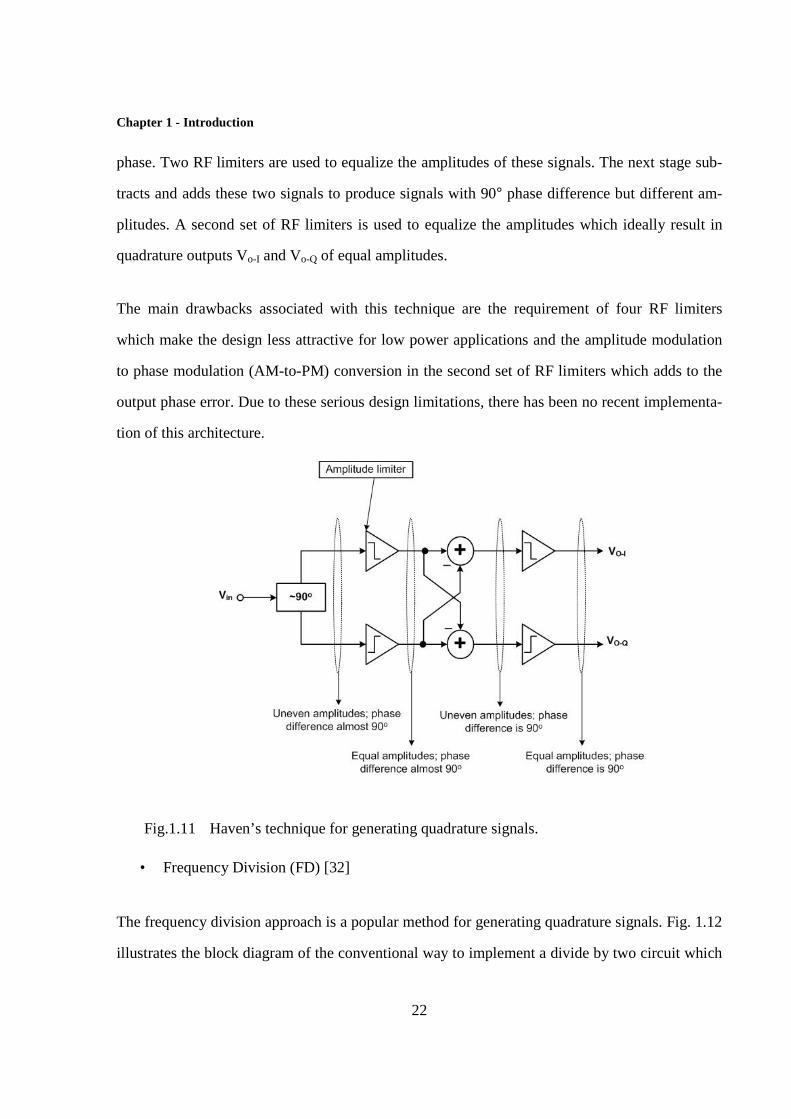
Chapter 1 - Introduction
22
phase. Two RF limiters are used to equalize the amplitudes of these signals. The next stage sub-
tracts and adds these two signals to produce signals with 90° phase difference but different am-
plitudes. A second set of RF limiters is used to equalize the amplitudes which ideally result in
quadrature outputs Vo-I and Vo-Q of equal amplitudes.
The main drawbacks associated with this technique are the requirement of four RF limiters
which make the design less attractive for low power applications and the amplitude modulation
to phase modulation (AM-to-PM) conversion in the second set of RF limiters which adds to the
output phase error. Due to these serious design limitations, there has been no recent implementa-
tion of this architecture.
Fig.1.11 Haven’s technique for generating quadrature signals.
• Frequency Division (FD) [32]
The frequency division approach is a popular method for generating quadrature signals. Fig. 1.12
illustrates the block diagram of the conventional way to implement a divide by two circuit which

Chapter 1 - Introduction
23
consists of a master-slave flip-flop to divide a signal with a frequency of 2ω (two times the de-
sired LO frequency) by a factor of two. The main issue linked with this approach is that generat-
ing and dividing the signal at a frequency of 2ω may consume more power or simply be impos-
sible due to technology limitation and cost, depending on the desired LO frequency. Another is-
sue that adds to the design complexity of the LO generation circuitry, is the deviation of the input
signal duty cycle from 50% which results in phase imbalance at the output.
Fig.1.12 Frequency division technique.
• Ring Oscillators (RO) [33]
Ring oscillators typically used as quadrature generators consist of four identical differential delay
cells as shown in Fig. 1.13. The delay across each cell is set to be equivalent to a phase shift of
90° in the signal. This architecture requires buffers at the output and three additional sets of
dummy buffers at the output of the remaining three delay cells to maintain the symmetry of the
design and equalize the delay through each delay cell, and is not suitable for low-power portable
applications. This approach is known for its relatively poor phase noise performance which
makes it unattractive for most wireless applications.

Chapter 1 - Introduction
24
Fig.1.13 Ring oscillator quadrature generator.
• Cellular Oscillator Networks (CON) [34]
The simplest form of a cellular oscillator network used to generate quadrature signal is shown in
Fig. 1.14. This approach is based on a simple form of the digital ring oscillator with an odd num-
ber of inverting amplifiers. It can be shown that if the inner loop (6-5-4) has larger driving force
than the outer loops (1-6-5, 6-2-4, 5-4-3) this circuit will start to oscillate [34]. The required
larger driving force for the inner loop is achieved by using larger transistors in the CMOS invert-
ers participating in the loop. The phase shift on each inverter on the outer border and the inner
loop will be 30° (360°/12, where, 12 is the number of inverters on the outer border) and 120°
(360°/3, where 3 is the number of inverters forming the inner loop) respectively. Therefore any
three consecutive inverters on the outer border will produce 90° of phase shift; an example of
two signals with 90° phase shift, labeled Vo-I and Vo-Q, is illustrated in Fig. 1.14. Twelve sets of I
and Q signals are generated by any three consecutive inverter on the outer border. This approach
offers relatively accurate quadrature phase and amplitude matching at the expense of high power
consumption due to the large number of inverters employed in the design. It also requires buffers
at every node of the circuit to preserve the symmetry of the design which is crucial to match the
delays at all the nodes in the circuit. Similar to RO, this approach presents relatively poor phase

Chapter 1 - Introduction
25
noise. Phase noise can be improved in CON at the expense of power consumption as in CMOS
inverters.
Fig.1.14 I/Q generation using CON.
• LC Quadrature Oscillators (LCQ) [35]
Fig. 1.15 shows the basic cell of a quadrature LC-oscillator. It consists of two identical LC-
oscillators coupled for quadrature outputs. This architecture requires perfect matching and sym-
metry among oscillators A and B to achieve precise quadrature oscillation [35]. This architecture
typically requires four inductors which consume a relatively big chip area, in addition the neces-
sity for two identical LC-oscillators makes the design power hungry which is not favorable for
portable applications.
Fig.1.15 Quadrature LC VCO.

Chapter 1 - Introduction
26
• Summary of Previous Quadrature Generator Work
Table 1.5 summarizes the state of the art reported quadrature generators designs. According to
the previous discussion on different types of quadrature generators and the state of the art works
listed in Table 1.5, it is observable that none of these simultaneously satisfy all the requirements
of future mobile phones in an efficient way.
Table 1.5 State of the Art Quadrature Generators
Parameter
RCF PPF FD RO CON* LCQ
[28] [40] [30] [41] [32] [42] [33] [34] [35] [43]
Technology (µµµµm) 0.35 0.065 0.18 0.18 0.18 0.09 0.18 0.5 0.18 0.13
Supply Voltage (v) --- 1.2 --- 1.8 1.8 0.09 1.8 3 1.8 1
Frequency (GHz) 2 2 2 10 2 7 3.5 4.66 2.5 2.1
Amplitude Mis-match (%)
7.5 12
< 2.8 2.9
< 9 ---
--- 0 < 5 2
Phase Mismatch (o) 4.5 5 < 2 1.5 < 2.5 7 < 3.2 < 1 < 1.2 2
Power Consump-tion (mW)
0 15
--- ---
--- 15.6
16.2 --- 7.2 0.6
Chip Area (mm2) --- --- --- --- --- --- --- --- 0.55 ---**
* Only simulation results were reported.
** Using BAW resonator which is installed inside package.
1.4 Objectives and Outline of the Thesis
As pointed out previously, the RF front-end’s linearity at low voltage supplies is one of the main
design challenges for future generation of mobile phone receivers. Furthermore, the linearity of
the mixer has considerable influence on the overall linearity of the RF front-end of the receiver.
The goal of this thesis is to devise a new architecture and design methodology for the implemen-

Chapter 1 - Introduction
27
tation of CMOS RF quadrature down-converters, operating at 8GHz, which simultaneously satis-
fy the low voltage and linearity requirements. The quadrature down-converter is intended to meet
the tentative target specifications obtained using MATLAB, listed in Table 1.2, and is to be im-
plemented in CMOS technology. A 0.18 µm CMOS technology was chosen for the implementa-
tion, since it is a well-established process which satisfies both the performance and the low cost
requirements envisaged.
Chapter 2 deals with the system level simulation of a direct conversion receiver in MATLAB
considering a wireless channel and an OFDM system. The effect of the quadrature down-
converter’s non-idealities on the performance of the OFDM system under consideration is stud-
ied in terms of the bit-error-rate (BER) of the received signal, and a set of tentative specifications
for the mixer and the quadrature generator is extracted to meet a target un-coded BER of 10-3.
In Chapter 3, the design, simulation and analysis of a new current commutating CMOS mixer is
presented [44, 45]. The main factors affecting the linearity of CMOS current commutating mix-
ers are discussed and a novel architecture, based on the bias-offset-technique is proposed to sim-
ultaneously satisfy the high linearity, low voltage and design simplicity requirements of the fu-
ture generation of mobile phones. A design methodology for the new architecture is also present-
ed.
The design methodology of a new quadrature generator based on a simple analytical model is
presented in Chapter 4 [46]. The design uses active inductors embodied in the LO-buffer and fea-
tures relatively low power consumption by omitting the buffers located between the quadrature
generator and the mixers. The coupling between amplitude tuning and quadrature phase tuning is
relaxed, allowing for relatively easy tuning and good quadrature phase and amplitude matching.

Chapter 1 - Introduction
28
Chapter 5 presents the implementation and experimental results of the quadrature generator and
the mixer [47], building the quadrature down-converter. Conclusions and guidelines for future
work are presented in Chapter 6.
In order to show the applicability of the proposed circuitry and associated design methodologies
to more advanced CMOS technologies, the circuitry are ported to TSMC 65nm technology, the
results of which is included in Appendix A.

Chapter 1 - Introduction
29
References
[1] Parssinen, A.; , "Multimode-multiband transceivers for next generation of wireless com-
munications," ESSCIRC (ESSCIRC), 2011 Proceedings of the, pp.25-36, 12-16 Sept. 2011.
[2] M. Lefevre and P. Okrah, “Making the Leap to 4G Wireless,” EE Times, Network, Communication System Design, pp. 26-32, July 2001.
[3] Y. Mochida, T. Takano, H. Gambe, “Future Directions and Technology Requirements of Wireless Communications,” IEEE International Electron Devices Meeting , Digest, pp. 1.3.1 - 1.3.8, 2001.
[4] H. Sampath, S. Talwar, J. Tellado, V. Erceg and A. Paulraj, “A fourth-generation MIMO-OFDM Broadband Wireless System: Design, Performance and Field Trial Results,” IEEE Communication Magazine, Vol. 40, Issue 9, pp. 143 - 149, 2002.
[5] F. Fitzek, A. Kopsel, A. Wolisz, M. Krishnam, M. Reisslein, “Providing Application-Level QOS in 3G/4G Wireless Systems: A Comprehensive Framework Based on Multi-rate CDMA,” IEEE Wireless Communications, Vol. 9, Issue 2, pp. 42 - 47, 2002.
[6] S. Mattisson, “Architecture and Technology for Multi-standard Transceivers,” Bipo-lar/BiCMOS Circuits and Technology Meeting, Proceedings, pp. 82-85, 2001.
[7] Darabi, H.; Chang, P.; Jensen, H.; Zolfaghari, A.; Lettieri, P.; Leete, J.C.; Mohammadi, B.; Chiu, J.; Qiang Li; Shr-Lung Chen; Zhimin Zhou; Vadipour, M.; Chen, C.; Yuyu Chang; Mirzaei, A.; Yazdi, A.; Nariman, M.; Hadji-Abdolhamid, A.; Ethan Chang; Zhao, B.; Juan, K.; Suri, P.; Guan, C.; Serrano, L.; Leung, J.; Shin, J.; Kim, J.; Tran, H.; Kilcoyne, P.; Vinh, H.; Raith, E.; Koscal, M.; Hukkoo, A.; Hayek, C.; Rakhshani, V.; Wilcoxson, C.; Rofougar-an, M.; Rofougaran, A.; , "A Quad-Band GSM/GPRS/EDGE SoC in 65 nm CMOS," Solid-State Circuits, IEEE Journal of , vol.46, no.4, pp.870-882, April 2011.
[8] J. C. Rudell, J. J. Ou, T. B. Cho, G. Chien, F. Brianti, J. A. Weldon, P. R. Gray, “A 1.9 GHz Wideband IF Double Conversion CMOS Receiver For Cordless Telephone Applica-tions,” IEEE Journal of Solid-State Circuits, Vol. 32, pp. 2071 - 2088, 1997.
[9] M. S. J. Steyaert, J. Janssens, B. de Muer, M. Borremans, N. Itoh, “A 2-V CMOS Cellular Transceiver Front-end,” IEEE Journal of Solid-State Circuits, Vol. 35, pp. 1895 - 1907, 2000.
[10] R.V.L. Hartley, “Modulation System,” US-Patent #1, 666, 206, 1928.
[11] D. K. Weaver, “A Third Method of Generation and Detection of Single-Sideband Sig-nals,” Proceedings of IRE, Vol. 44, pp. 1703 - 1705, 1956.
[12] A.K. Salkintzis, N.Hong, P. T. Mathiopoulos, “ADC and DSP Challenges in the Devel-opment of Software Radio Base stations,” IEEE Personal Communications, Vol. 6, Issue 4, pp. 47 - 55, 1999.

Chapter 1 - Introduction
30
[13] D. Manstretta, R. Castello, F. Gatta, P. Rossi, F. Svelto, “A 0.18µm CMOS Direct-Conversion Receiver Front-end for UMTS,” International Solid-State Circuits Conference, Technical Digest, pp. 240 - 463, 2002.
[14] B. Razavi, “Design Considerations for Direct-Conversion Receivers,” IEEE Transactions on Circuit and Systems - II: Analog and Digital Signal Processing, Vol. 44, pp. 428 - 435, 1997.
[15] A.A. Abidi, “Direct-Conversion Radio Transceivers for Digital Communications,” IEEE Journal of Solid-State Circuits, Vol. 30, pp. 1399 - 1410, 1995.
[16] J. K. Cavers and M. W. Liao, “Adaptive Compensation for Imbalance and Offset Losses in Direct Conversion Transceivers,” IEEE Transactions on Vehicular Technology, Vol. 42, pp. 581 - 588, 1993.
[17] M. Faulkner, “DC offset and IM2 Removal in Direct Conversion Receivers,” IEE pro-ceedings of Communications, Vol. 149, Issue: 3, pp. 179 - 184, 2002.
[18] J. F. Wilson, R. Youell, T. H. Richards, G. Luff, R. Pilaski, “A Single-chip VHF and UHF Receiver for Radio Paging,” IEEE Journal of Solid-State Circuits, Vol. 26, pp. 1944 - 1950, 1991.
[19] IEEE Std 802.11a, Wireless LAN Medium Access Control (MAC) and Physical Layer (PHY) Specifications: High-Speed Physical Layer in the 5 GHz Band, IEEE, 1999.
[20] E. E. Bautista, B. Bastani and J. Heck, “A high IIP2 Down-conversion Mixer Using Dy-namic Matching,” IEEE Journal of Solid-State Circuits, Vol. 35, pp. 1934 - 1941, 2000.
[21] R. C. Sagers, “Intercept Point and Undesired Responses,” IEEE Transactions on Vehicu-lar Technology, Vol. 32, pp. 121 - 133, 1983.
[22] Soer, M.C.M.; Klumperink, E.A.M.; de Boer, P.-T.; van Vliet, F.E.; Nauta, B.; , "Unified Frequency-Domain Analysis of Switched-Series- Passive Mixers and Samplers," Circuits and Systems I: Regular Papers, IEEE Transactions on , vol.57, no.10, pp.2618-2631, Oct. 2010.
[23] Q. Li, J. Zhang, W. Li and J. S. Yuan, “CMOS RF Mixer Non-Linearity Design,” IEEE 43rd Midwest symposium on Circuits and Systems, pp. 808 - 811, 2001.
[24] S. J. Fang, S. T. Lee, D. J. Allstot and A. Bellaouar, “A 2 GHz CMOS Even Harmonic Mixer for Direct Conversion Receivers,” International Symposium on Circuits and Systems, Vol. 4, pp. 708 - 710, 2002.
[25] P. J. Sullivan, B. A. Xavier and W. H, Ku, “Doubly balanced Dual Gate CMOS Mixer,” IEEE Journal of Solid-State Circuits, Vol. 34, pp. 878 - 881, 1999.
[26] H. M. Wang, “A 1-V Multi-Gigahertz RF Mixer Core in 0.5-m CMOS,” IEEE Journal of Solid-State Circuits, Vol. 33, pp. 2265 - 2267, 1998.

Chapter 1 - Introduction
31
[27] T. H. Lee, “The Design of CMOS Radio Frequency Integrated Circuits,” Cambridge University Press, 2001, Chapter 18, PP. 559.
[28] D. H. Sim, “CMOS I/Q Demodulator Using a High-Isolation and Linear Mixer for 2GHz Operation,” IEEE Radio Frequency Integrated Circuit Symposium, pp. 61 - 64, 2004.
[29] M. J. Gingell, “Polyphase Symmetrical Network,” US-Patent #3,559,042, 1971.
[30] K. Koh, M. Park, C. Kim and H. Yu, “Subharmonically Pumped CMOS Frequency Con-version (Up and Down) Circuits for 2-GHz WCDMA Direct-Conversion Transceiver,” IEEE Journal of Solid-State Circuits, Vol. 39, pp. 871 - 884, 2004.
[31] A. Koullias, J. H. Havens, I. G. Post and P. E. Bronner, “A 900 MHz Transceiver Chip Set for Dual-Mode Cellular Radio Mobile Terminals,” IEEE International Solid-State Circuit Conference (ISSCC), Digest of Technical Papers, pp. 140-141, 278 1993.
[32] F. Gatta, D. Manstretta, P. Rossi and F. Svelto, “A Fully Integrated 0.18-m CMOS Di-rect Conversion Receiver Front-End With On-Chip LO for UMTS,” IEEE Journal of Solid-State Circuits, Vol. 39, pp. 15 - 23, 2004.
[33] M. Grozing, B. Phillip and M. Berroth, “ CMOS Ring Oscillator with Quadrature Outputs and 100 MHz to 3.5 GHz Tuning Range,” European Solid-State Circuits Conference, pp. 679 - 682, 2003.
[34] S. Hwang, G. Moon and S. Song, “A GHz I-Q Quadrature Signal Generator using Cellu-lar Oscillator Network,” IEEE Asia Pacific Conference on Application Specific Integrated Circuits, pp. 91-94, 1999.
[35] D. Leenaerts, C. Dijkmans and M. Thompson, “A 0.18m CMOS 2.45 GHz Low-Power Quadrature VCO with 15% Tuning Range,” IEEE Radio Frequency Integrated Circuit Sym-posium, pp. 67 - 69, 2002.
[36] Fan Xiangning; Zhang Lei; Zhu Chisheng; Wu Rui; , "Implementation of an improved active CMOS mixer with high linearity for wideband wireless systems," Signals Systems and Electronics (ISSSE), 2010 International Symposium on , vol.2, pp.1-4, 17-20 Sept. 2010.
[37] Gao Junjun; Cheng Zhiqun; Zhu Xuefang; Xu Shengjun; , "A high performance CMOS even harmonic mixer with a LC resonant circuit," Microwave and Millimeter Wave Technol-ogy (ICMMT), 2010 International Conference on, pp.449-453, 8-11 May 2010.
[38] Hyo-Rim Bae; Choon Sik Cho; Lee, J.W.; Jaeheung Kim; , "A 24GHz dual-gate mixer using sub-harmonic in 0.18µm CMOS technology," Microwave Conference, 2009. APMC 2009. Asia Pacific, pp.1739-1742, 7-10 Dec. 2009.
[39] Van Vorst, D.; Mirabbasi, S.; , "Low-power 1V 5.8 GHz bulk-driven mixer with on-chip balun in 0.18µm CMOS," Radio Frequency Integrated Circuits Symposium, 2008. RFIC 2008. IEEE , pp.197-200, June 17 2008-April 17 2008.
[40] Roufoogaran, R.; Li, T.; Ojo, A.; Cheng, S.; Lee, C.P.; Mahadeva, S.; Shetter, P.; Behzad, A.; , "A compact and power efficient local oscillator generation and distribution sys-
Chapter 1 - Introduction
32
tem for complex multi radio systems," Radio Frequency Integrated Circuits Symposium, 2008. RFIC 2008. IEEE , pp.277-280, June 17 2008-April 17 2008.
[41] Syu, J.-S.; Meng, C.; Teng, Y.-H.; , "10 GHz dual-conversion low-IF downconverter with microwave and analogue quadrature generators," Electronics Letters , vol.45, no.13, pp.685 -686, June 18 2009.
[42] Hara, S.; Okada, K.; Matsuzawa, A.; , "10MHz to 7GHz quadrature signal generation us-ing a divide-by-4/3, -3/2, -5/3, -2, -5/2, -3, -4, and -5 injection-locked frequency divider," VLSI Circuits (VLSIC), 2010 IEEE Symposium on , pp.51-52, 16-18 June 2010.
[43] Rai, S.; Otis, B.; , "A 1V 600µW 2.1GHz Quadrature VCO Using BAW Resonators," Solid-State Circuits Conference, 2007. ISSCC 2007. Digest of Technical Papers. IEEE Inter-national , pp.576-623, 11-15 Feb. 2007.
[44] F. Mahmoudi and C.A.T. Salama, “Low-Voltage, Low-Power, High Linearity, Active CMOS Mixer,” US Patent, Publication # 2005-0124311-A1.
[45] F. Mahmoudi and C. A. T. Salama, “8 GHz, 1V, High Linearity, Low Power CMOS Ac-tive Mixer,” IEEE Radio Frequency Integrated Circuit Symposium, pp. 401 - 404, 2004.
[46] F. Mahmoudi and C. A. T. Salama, “8 GHz Tunable CMOS Quadrature Generator using Differential Active Inductors,” IEEE International Symposium on Circuits and Systems, pp. 2112 - 2115, 2005.
[47] F. Mahmoudi and C. A. T. Salama, “8GHz 1V, CMOS Quadrature Downconverter for Wireless Applications,” Analog Integrated Circuits and Signal Processing, Vol.48, No.3, June 2006, pp.185-197.

Chapter 2- Downconverter System Level Simulations
33
CHAPTER 2
CHAPTER 2: Down-converter System Level Simulations
2.1 Introduction
The relatively wide bandwidth targeted by future generation of mobile phones translates into
demanding system and circuit level requirements. In this chapter, system level simulations are
carried out; using MATLAB on a direct conversion receiver (DCR) to understand the effect of
quadrature down-converter impairments on the performance of the whole receive chain,
including the baseband circuitry. A set of tentative specifications are also extracted for the mixer
and the quadrature generator, assuming OFDM as the multiple access scheme.
2.2 OFDM Communication System
Fig. 2.1 shows a typical OFDM communication system. The data and OFDM
modulation/demodulations are performed in the digital part of the transceiver. The analog
portion of the system consists of the transmitter, the wireless channel and the receiver. The
channel is modeled as a Rayleigh fading channel1. The receiver was intended to satisfy a target
un-coded BER of 10-3 [1].
1 See MATLAB codes located at: http://www.vrg.utoronto.ca/~ngwt/Resources/MATLAB/DCR.

Chapter 2- Downconverter System Level Simulations
34
Fig.2.1 Typical OFDM Communication system.
A typical receiver block is shown in Fig. 2.2 in detail. This scheme was used in modeling the
receiver. The receiver consists of two RF low-noise-amplifiers (LNA), two RF band-select
filters, single-ended to differential converter balun, attenuator, down-conversion mixer, baseband
low-pass filter, baseband variable-gain-amplifier (VGA), anti-alias filter and analog to digital
converter.
Fig.2.2 Typical direct conversion receiver block diagram [2].
The OFDM modulator/demodulator was modeled as shown in Fig. 2.3. As observed in the
figure, the modulator first converts the data from a serial stream to parallel sets. The parallel data
is then modulated to the orthogonal carrier frequencies. The inverse-fast-Fourier-transform
(IFFT) converts the parallel data into time domain waveforms. Finally, these waveforms are
combined to create a single time domain signal for transmission. In the demodulator, the

Chapter 2- Downconverter System Level Simulations
35
received data is first converted to parallel data streams. The FFT block converts the parallel data
into frequency domain data; at this point the data is available in modulated form on the
orthogonal carriers. A final demodulation step recovers the data. The parallel to serial converter
then converts the parallel data to a serial stream to recover the original signal. Table 2.1
summarizes the parameters used for MATLAB simulation of the OFDM system under
consideration based on the system configuration in Fig. 2.3. The cyclic extension parameter,
listed in the Table, refers to the redundancy added to the symbols to reduce or eliminate inter-
symbol interference due to delay spread in the wireless channel.
Fig.2.3 OFDM modulator and demodulator block diagram [2].
Table.2.1 Specifications of the OFDM System Under Consideration
Value
Number of Subcarriers 1024
IFFT/FFT Size 1024
Subcarrier Spacing 25 KHz
Cyclic Extension Duration 15% of a Symbol
Subcarrier Modulation 64QAM
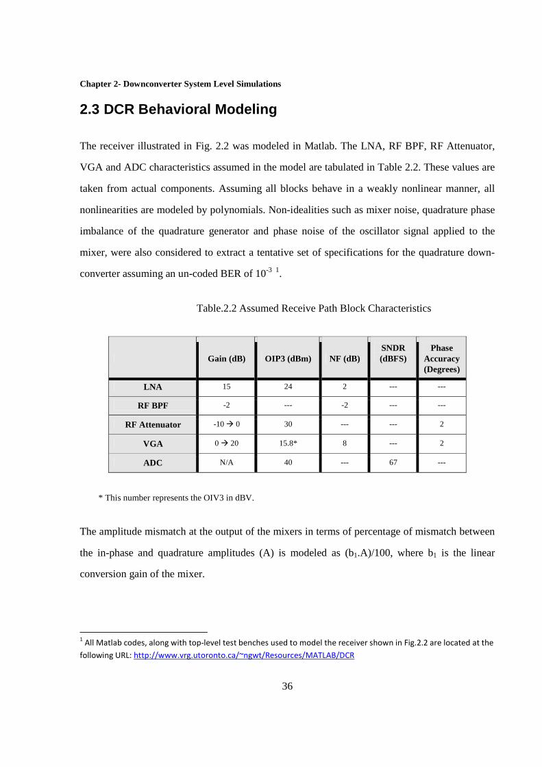
Chapter 2- Downconverter System Level Simulations
36
2.3 DCR Behavioral Modeling
The receiver illustrated in Fig. 2.2 was modeled in Matlab. The LNA, RF BPF, RF Attenuator,
VGA and ADC characteristics assumed in the model are tabulated in Table 2.2. These values are
taken from actual components. Assuming all blocks behave in a weakly nonlinear manner, all
nonlinearities are modeled by polynomials. Non-idealities such as mixer noise, quadrature phase
imbalance of the quadrature generator and phase noise of the oscillator signal applied to the
mixer, were also considered to extract a tentative set of specifications for the quadrature down-
converter assuming an un-coded BER of 10-3 1.
Table.2.2 Assumed Receive Path Block Characteristics
Gain (dB) OIP3 (dBm) NF (dB) SNDR (dBFS)
Phase Accuracy (Degrees)
LNA 15 24 2 --- ---
RF BPF -2 --- -2 --- ---
RF Attenuator -10 0 30 --- --- 2
VGA 0 20 15.8* 8 --- 2
ADC N/A 40 --- 67 ---
* This number represents the OIV3 in dBV.
The amplitude mismatch at the output of the mixers in terms of percentage of mismatch between
the in-phase and quadrature amplitudes (A) is modeled as (b1.A)/100, where b1 is the linear
conversion gain of the mixer.
1 All Matlab codes, along with top-level test benches used to model the receiver shown in Fig.2.2 are located at the
following URL: http://www.vrg.utoronto.ca/~ngwt/Resources/MATLAB/DCR
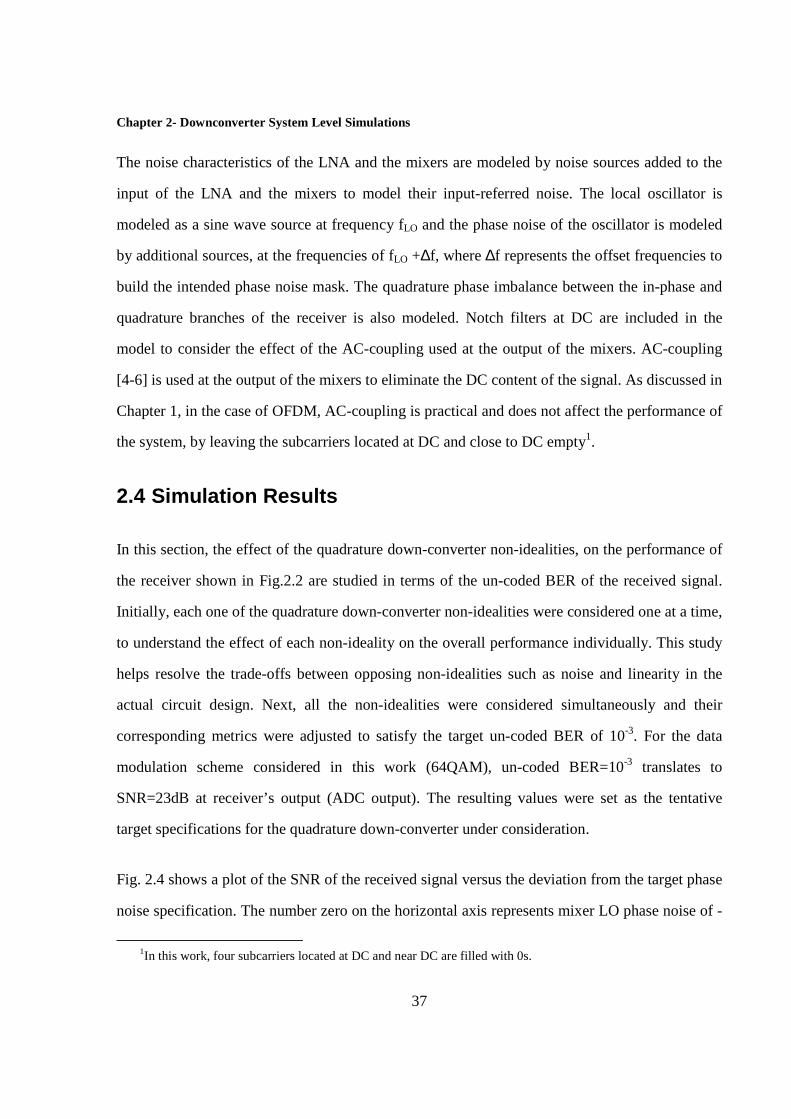
Chapter 2- Downconverter System Level Simulations
37
The noise characteristics of the LNA and the mixers are modeled by noise sources added to the
input of the LNA and the mixers to model their input-referred noise. The local oscillator is
modeled as a sine wave source at frequency fLO and the phase noise of the oscillator is modeled
by additional sources, at the frequencies of fLO +∆f, where ∆f represents the offset frequencies to
build the intended phase noise mask. The quadrature phase imbalance between the in-phase and
quadrature branches of the receiver is also modeled. Notch filters at DC are included in the
model to consider the effect of the AC-coupling used at the output of the mixers. AC-coupling
[4-6] is used at the output of the mixers to eliminate the DC content of the signal. As discussed in
Chapter 1, in the case of OFDM, AC-coupling is practical and does not affect the performance of
the system, by leaving the subcarriers located at DC and close to DC empty1.
2.4 Simulation Results
In this section, the effect of the quadrature down-converter non-idealities, on the performance of
the receiver shown in Fig.2.2 are studied in terms of the un-coded BER of the received signal.
Initially, each one of the quadrature down-converter non-idealities were considered one at a time,
to understand the effect of each non-ideality on the overall performance individually. This study
helps resolve the trade-offs between opposing non-idealities such as noise and linearity in the
actual circuit design. Next, all the non-idealities were considered simultaneously and their
corresponding metrics were adjusted to satisfy the target un-coded BER of 10-3. For the data
modulation scheme considered in this work (64QAM), un-coded BER=10-3 translates to
SNR=23dB at receiver’s output (ADC output). The resulting values were set as the tentative
target specifications for the quadrature down-converter under consideration.
Fig. 2.4 shows a plot of the SNR of the received signal versus the deviation from the target phase
noise specification. The number zero on the horizontal axis represents mixer LO phase noise of -
1In this work, four subcarriers located at DC and near DC are filled with 0s.

Chapter 2- Downconverter System Level Simulations
38
105dBc/Hz at 1MHz offset, which means the phase noise is varied from -115dBc/Hz to -
95dBc/Hz at 1 MHz offset.
Based on Fig.2.4, the phase noise performance of the quadrature generation circuitry should be
better than -105dBc/Hz at 1MHz offset to guaranty SNR better than 23dB. The LO phase noise
mask corresponding to the zero on the horizontal axis of Fig.2.4 is illustrated in Fig.2.5.
Fig.2.4 SNR versus phase noise of the mixer LO CLK.
Fig.2.5 Mixer LO phase-noise mask meeting BER spec of 10-3.

Chapter 2- Downconverter System Level Simulations
39
The effect of the I/Q phase imbalance in a DCR on the performance of the OFDM system is
shown in Fig. 2.6. The quadrature phase imbalance is defined as the deviation from 90° in the
phases of the I with respect to the Q channel. Assuming quadrature phase error being the only
non-ideality in the receive chain, the maximum tolerable quadrature phase error is 4 degrees in
the system under consideration in order to maintain BER better than 10-3. As observed from the
plot, quadrature phase error below 2 degrees does not cause any bit error in the received signal.
A similar simulation assuming 16QAM data modulation (instead of 64QAM assumed for this
work), suggests the DCR is insensitive to phase error below 3o. This observation reinforces the
fact that communication system level specifications directly affect circuit level requirements.
Fig.2.6 Receiver BER versus quadrature phase error.
Quadrature phase error spec also depends on IRR requirement. Typical IRR requirement for
DCRs is 40dB [3] which translates into quadrature phase accuracy of better than 2o.
The nonlinearity of the mixer also affects the performance of the OFDM system by introducing
inter-symbol interference (ISI) and intermodulation distortion components in the band of interest
of the received signal. Fig. 2.7 illustrates the SNR performance of the DCR versus mixer IIP3.
Chapter 2- Downconverter System Level Simulations
40
As observed from the figure, Mixer’s IIP3 should be better than +3dBm to meet the target 23dB
system SNR.
Fig.2.7 System-level SNR in terms of mixer linearity.
The maximum allowed noise contribution by the receiver is characterized with its Noise Figure
(NF). The required NF of wireless receivers are extracted from their target sensitivity, defined as
the minimum detectable signal at the receiver’s input. In this work the noise floor at the receiver
antenna is calculated as -174dBm/Hz1, and the target minimum detectable signal is set to -
97dBm2. Given the fact that minimum required SNR to successfully demodulate 64QAM data at
the output of the receiver is 23dB, the maximum allowed NF for the complete front-end is
calculated to be 4.78dB3 with sub-carrier bandwidth of 16.28KHz.
1 This number represents the thermal noise floor of the antenna assuming 50Ω antenna impedance at 300oK.
2 The LTE standard which is the closest industry-defined standard to this work, assumes -106.8dBm sensitivity for 1.4MHz bandwidth and -101.5dBm for 20MHz bandwidth. In a given wireless standard, sensitivity scales with tar-get bandwidth to maintain constant SNR. In this work, -97dBm sensitivity is assumed for bandwidth above 50MHz.
3 ( )[ ] SNRBWLOGRXNF SENSRX −+−−= 10174 where NFRX, RXSENS, BW and SNR represent the complete receiver’s noise
figure, the desired receiver’s sensitivity, sub-carrier bandwidth and required SNR at receiver’s output, respectively.

Chapter 2- Downconverter System Level Simulations
41
The maximum allowed NF calculated above includes the loss associated with the antenna
system. Assuming a typical antenna system loss of 1.5dB, results in a complete receiver NF
requirement of 3.2dB. The NF target for this work is set to 3dB.
Fig.2.8 illustrates the effect of mixer NF on the overall receiver NF. This plot depends strongly
on the noise and gain characteristics of all blocks preceding the mixer. This plot is generated
assuming the rest of the receiver components performance is as listed in Table 2.2, it assumes
VGA and mixer gain of 6dB each.
Fig.2.8 Overall system noise figure in terms of mixer noise figure.
As observed from Fig.2.8, the mixer NF should be below 16dB over the band of interest to
guaranty an overall receiver NF better than 3dB.
In order to extract a set of quadrature down-converter target specification for the communication
system described in this chapter, All the quadrature down-converter non-idealities were applied
simultaneously in the MATLAB model1. the quadrature down-converter performance metrics
were interactively varied to guaranty an SNR above 23dB or equivalently un-coded BER of 10-3
1 MATLAB model is located at: http://www.vrg.utoronto.ca/~ngwt/Resources/MATLAB/DCR.

Chapter 2- Downconverter System Level Simulations
42
at the receiver’s output. The resulting values are listed in Table 2.3. These values were set as
tentative target specifications for the quadrature down-converter designed in this work. The
numbers listed in Table 2.3 are applicable when all non-idealities are simultaneously applied to
the model, as would be the case in practice.
Table.2.3 Tentative Specifications for the Mixer and Quadrature Generator
Circuit Parameter Value
Mixer
IIP2* > 50 dBm
IIP3 > 3 dBm
Noise Figure <13 dB
Quadrature Generator
Phase noise @ 1MHz offset <-110dBc/Hz
I/Q phase mismatch <2°
Quadrature Downconverter
Image Rejection Ratio (IRR)
>40 dB
* In a DCR, the IIP2 spec is mainly determined by the out of band linearity requirements, which in terms depends on the detailed system specification and amount of available out of band filtering. The target of 50dBm is arbitrary chosen to remain competitive to the state of the art in the literature.
2.5 Summary
All blocks in a direct conversion OFDM receiver (DCR) were modeled at the behavioral level in
MATLAB. The wireless channel was modeled as a Rayleigh fading channel. The effect of all
non-idealities associated with the quadrature down-converter in a DCR on the performance of
the OFDM system were individually examined in terms of the un-coded bit-error-rate (BER) of
the received signal, or equivalently SNR at the output of the receiver. Tentative specifications for
the quadrature down-converter building blocks were extracted. This was done while all non-
idealities were simultaneously applied to the receiver.

Chapter 2- Downconverter System Level Simulations
43
These specifications were considered while applying the new low-voltage, low power design
technique proposed in this work to an 8GHz quadrature down-converter.

Chapter 2- Downconverter System Level Simulations
44
References
[1] H. Liu, H. Ma, M. El Zarki and S. Gupta, “Error Control Schemes for Networks: An Overview”, Mobile Networks and Applications II, pp. 167 - 182, 1997.
[2] A. R. S. Bahai, Burton R. Saltzberg and M. Ergen, Multi-Carrier Digital Communications Theory and Applications of OFDM, Springer, Second Edition, 2004.
[3] J. P. Maligeorgos and John R. Long, “A Low-Voltage 5.1-5.8 GHz Image Reject Receiver with Wide Dynamic Range,” IEEE Journal of Solid-State Circuits, Vol. 35, pp. 1917 - 1926, 2000.

Chapter 3 - CMOS Downconversion Mixer
45
CHAPTER 3: CMOS Down-conversion Mixer
3.1 Introduction
The design, layout and post layout simulation of an 8 GHz down-conversion mixer are discussed
in this chapter. Linearization techniques for current commutating mixers are briefly mentioned
and the circuit of the proposed mixer and its evolution from the bias offset technique, originally
applied to differential pair CMOS trans-conductors, are discussed. The mixer’s design
methodology and characteristics are also presented.
3.2 Current Commutating Mixers
The current commutating mixer (CCM) is the most widely used CMOS mixer [1] because it
offers advantages such as relatively high conversion gain and high port-to-port isolation. CCMs
which are based on the multiplication of two signals, exhibit superior performance compared to
other CMOS mixers as discussed in Chapter 1. Furthermore, the principle of operation of the
CCM is technology independent1 which makes it easier to migrate from one technology to
another.
The block diagram and a conventional CMOS implementation of the current commutating mixer
are illustrated in Fig. 3.1. As observed from Fig. 3.1(a), the CCM consists of a trans-conductor to
1Regardless of the technology used: CMOS, BICMOS or Bipolar (and its variants), the conventional CCM consists of a trans-conductor followed by switching pairs to perform the frequency translation.

Chapter 3 - CMOS Downconversion Mixer
46
convert the incoming voltage to current, followed by a mixing stage to perform the frequency
translation, and finally a trans-impedance stage to convert the resulting down-converted current
back to voltage. Fig. 3.1(b) shows a conventional implementation of the CCM using MOSTs. In
what follows, the three main blocks involved in a CCM are briefly discussed.
(a)
(b)
Fig.3.1 Current commutating mixer (CCM). (a) Block diagram of the CCM. (b) Conventional circuit diagram of the CCM.

Chapter 3 - CMOS Downconversion Mixer
47
3.5.1 Trans-conductor
The trans-conductance stage of a CCM can be implemented using either common-gate or
common-source stages [2,3]. Both single ended and differential implementations are possible.
Various options for differential implementations of these configurations are illustrated in Fig.
3.2. Figs. 3.2(a)-(c) illustrate the common-gate implementations and Figs. 3.2(d)-(f) illustrate the
common-source implementations. Some trans-conductors use a combination of Fig.3.2 (d) and
(e) configurations.
Fig.3.2 Various conventional possibilities to implement trans-conductors. (a)-(c) Common gate implementations. (d)-(f) Common source implementations.
3.5.2 Mixing Stage
The mixing stage of a CCM performs the frequency translation, and typically consists of cross-
coupled differential pairs as shown in Fig. 3.3. The bias of the transistors in the mixing stage and
the amplitude of the local oscillator signal, denoted as Vin-LO are typically chosen such that the
transistors act as close as possible to ideal switches. The closer to ideal switching, the better the

Chapter 3 - CMOS Downconversion Mixer
48
performance of the complete CCM in terms of conversion gain and noise figure is. The
maximum theoretical conversion gain for an ideal mixing stage as shown in Fig.3.3 is π/4.
Fig.3.3 Cross-coupled differential pairs as mixing stage.
3.5.3 Trans-impedance Stage
The trans-resistance stage converts the down-converted current at IF back to voltage. It may be
implemented using resistors or active loads, or a combination of the two to provide adjustability
to the load resistance and achieve offset or device mismatch cancellation [4].
As mentioned in Chapter 1, achieving good linearity at low supply voltages is one of the main
challenges in the design of future generations CMOS RF receiver front-ends. In the next section,
the linearization techniques previously applied to the CCM are briefly discussed.
3.3 CCM Linearization Techniques
Linearization techniques previously proposed to improve the linearity characteristics of CCMs
include: source degeneration (SDE) [5], dynamic matching (DMA) [6], cross coupled
transconductors (CCT) [7], a CMOS pair (CMP) [8] and class A-B transconductors (ABT) [9].
These approaches are briefly discussed in the next few paragraphs.

Chapter 3 - CMOS Downconversion Mixer
49
3.3.1 Source Degeneration (SDE)
Fig. 3.4 shows the circuit diagram of a CCM with source degeneration [5]. Both resistive and
inductive source degeneration is possible. Typically, resistive degeneration is more suitable for
wideband applications at the expense of voltage headroom loss, while inductive degeneration
works only for narrow band applications due to its frequency selectivity.
Fig.3.4 Conventional CCM using source degeneration for linearizing the mixer.
The source degeneration resistor or inductor acts as a series-series feedback which reduces the
trans-conductance gain of the circuit while improving its linearity. This technique is popular for
bipolar transistors [10]. However it is not as efficient in the case of MOST differential pairs
because the trans-conductance of a MOST is typically lower than its bipolar counterpart.
3.3.2 Dynamic Matching (DMA)
Dynamic matching involves enhancing the balance of a fully differential mixer through
decreasing both component and device mismatches [6]. It basically moves the second order

Chapter 3 - CMOS Downconversion Mixer
50
intermodulation products and flicker noise created by the mixer, to frequency bands outside the
down-converted bandwidth of interest. A CMOS implementation of this technique is shown in
Fig. 3.5. Differential clocks operating at higher frequencies than the channel bandwidth of
interest are necessary [6].
Fig.3.5 Linearized CCM using dynamic matching technique.
3.3.3 Cross-Coupled Trans-conductor (CCT)
In this approach, the differential pair trans-conductance of the conventional CCM is replaced by
two cross-coupled differential pairs as illustrated in Fig. 3.6 [7]. The objective is to have the
nonlinearities of the two differential pairs cancel out. The power consumption of this technique
can be close to twice the power consumption of the conventional CCM, depending on the
relative size of the two cross-coupled differential pairs.

Chapter 3 - CMOS Downconversion Mixer
51
Fig.3.6 Linearized CCM using cross-coupled trans-conductors.
3.3.4 Trans-conductor Using a CMOS Pair (CMP)
In this approach, the linearity of the CCM is improved by merging the trans-conductance stage
and the mixing stage in the form of a CMOS pair [12], as depicted in Fig. 3.7 [8]. This technique
works only if the MOST obeys the well-known quadratic behaviour in the saturation region of
operation. However, in modern deep submicron CMOS technologies, where the I-V transfer
characteristics of the MOS transistors are no longer quadratic, the effectiveness of this technique
is reduced. Furthermore, the CMOS pair is equivalent to a single transistor with a threshold
voltage equal to the sum of the absolutes of the threshold voltages of the N-channel and P-
channel transistors. This results in an equivalent threshold voltage roughly twice that of a single
transistor making the approach impractical for low-voltage designs.

Chapter 3 - CMOS Downconversion Mixer
52
Fig.3.7 Linearized CCM using CMOS pair.
3.3.5 Class A-B Trans-conductor (ABT)
In this CCM linearization approach, the nonlinear class-A trans-conductor of the conventional
CCM is replaced by a class AB trans-conductor stage [9]. This design provides 1.4 times the
input signal range of a simple differential pair (class A) trans-conductor, and results in more
linear trans-conductance range with respect to the input signal. The circuit diagram of a CCM
using the class AB trans-conductor is shown in Fig. 3.8. The technique improves the linearity of
the trans-conductance stage at the expense of increasing the power consumption and degrading
the noise figure characteristics of the design.
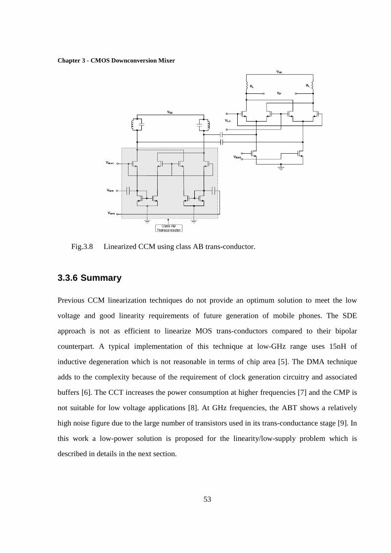
Chapter 3 - CMOS Downconversion Mixer
53
Fig.3.8 Linearized CCM using class AB trans-conductor.
3.3.6 Summary
Previous CCM linearization techniques do not provide an optimum solution to meet the low
voltage and good linearity requirements of future generation of mobile phones. The SDE
approach is not as efficient to linearize MOS trans-conductors compared to their bipolar
counterpart. A typical implementation of this technique at low-GHz range uses 15nH of
inductive degeneration which is not reasonable in terms of chip area [5]. The DMA technique
adds to the complexity because of the requirement of clock generation circuitry and associated
buffers [6]. The CCT increases the power consumption at higher frequencies [7] and the CMP is
not suitable for low voltage applications [8]. At GHz frequencies, the ABT shows a relatively
high noise figure due to the large number of transistors used in its trans-conductance stage [9]. In
this work a low-power solution is proposed for the linearity/low-supply problem which is
described in details in the next section.

Chapter 3 - CMOS Downconversion Mixer
54
3.4 Low-Voltage, High-Linearity Mixer Design Issues
In this section, the linearity characteristics of the main blocks involved in the CCM are
discussed.
3.4.1 Effect of the Trans-impedance Stage on the Linearity of CCM
As mentioned previously, the trans-impedance stage of a CCM may be implemented using
resistors or transistors. Trans-impedance blocks implemented using resistors are typically
expected to be more linear than those implemented using transistors since resistors ideally1 have
a linear behaviour. In the case of integrated resistors, depending on their type and the frequency
of operation they may exhibit nonlinear behaviour which is mainly attributed to the nonlinear
parasitic capacitances associated with the integrated resistors. At low frequencies2, the effect of
the parasitic capacitances on the linearity characteristics of the integrated resistors is negligible.
3.4.2 Effect of the Mixing Stage on the Linearity of CCM
The effect of the mixing stage of a CCM shown in Fig. 3.4 on linearity has been previously
investigated in the literature [15]. It depends to a great extent on the frequency of operation. At
low frequencies where the parasitic capacitances associated with the transistors are negligible,
the nonlinearity of the switching pairs is low and increases at higher frequencies where the
parasitic capacitances and their nonlinear behaviour come into play. Although the nonlinearity of
the mixing stage becomes more pronounced at higher frequencies, the trans-conductor stage is
1 Due to the voltage coefficient present in integrated resistors (IR) caused by the end effects, IRs may show nonline-ar behaviour. This behaviour depends mainly on resistors aspect ratio and width. This should be considered while choosing the aspect ratio and width of the resistor. In TSMC 0.18m CMOS width>1m and aspect ratio >2 should be chosen to ensure perfect linearity of resistors.
2 Baseband frequency in a direct conversion receiver (DCR).

Chapter 3 - CMOS Downconversion Mixer
55
still the dominant source of nonlinearity in a conventional CCM compared to the mixing stage
[15].
3.4.3 Effect of the Trans-conductor on the Linearity of CCM
In a conventional CCM, with a trans-conductor implemented using a simple differential pair, as
illustrated in Fig. 3.9(a), The differential pair has a nonlinear voltage to current transfer
characteristics resulting in a non-constant trans-conductance (Gm) as shown in Figs. 3.9(b) and
(c) respectively, which degrades the linearity of the CCM.
Fig.3.9 Conventional trans-conductor in CCM. (a) Circuit diagram. (b) Actual and ideal I-V transfer curves. (c) Actual and ideal trans-conductance.
In older generations of CMOS technology in which the MOSTs feature a quadratic behaviour in
the active region of operation, the relationship between the output differential current Io=Io1-Io2
and the input differential voltage Vi in Fig. 3.9(a) is given by the following nonlinear relationship
I o2 I o1– β V i
2Iβ----- V i
2–⋅ ⋅= (3.1)
where
β 12---µnC ox
W
L-----= (3.2)
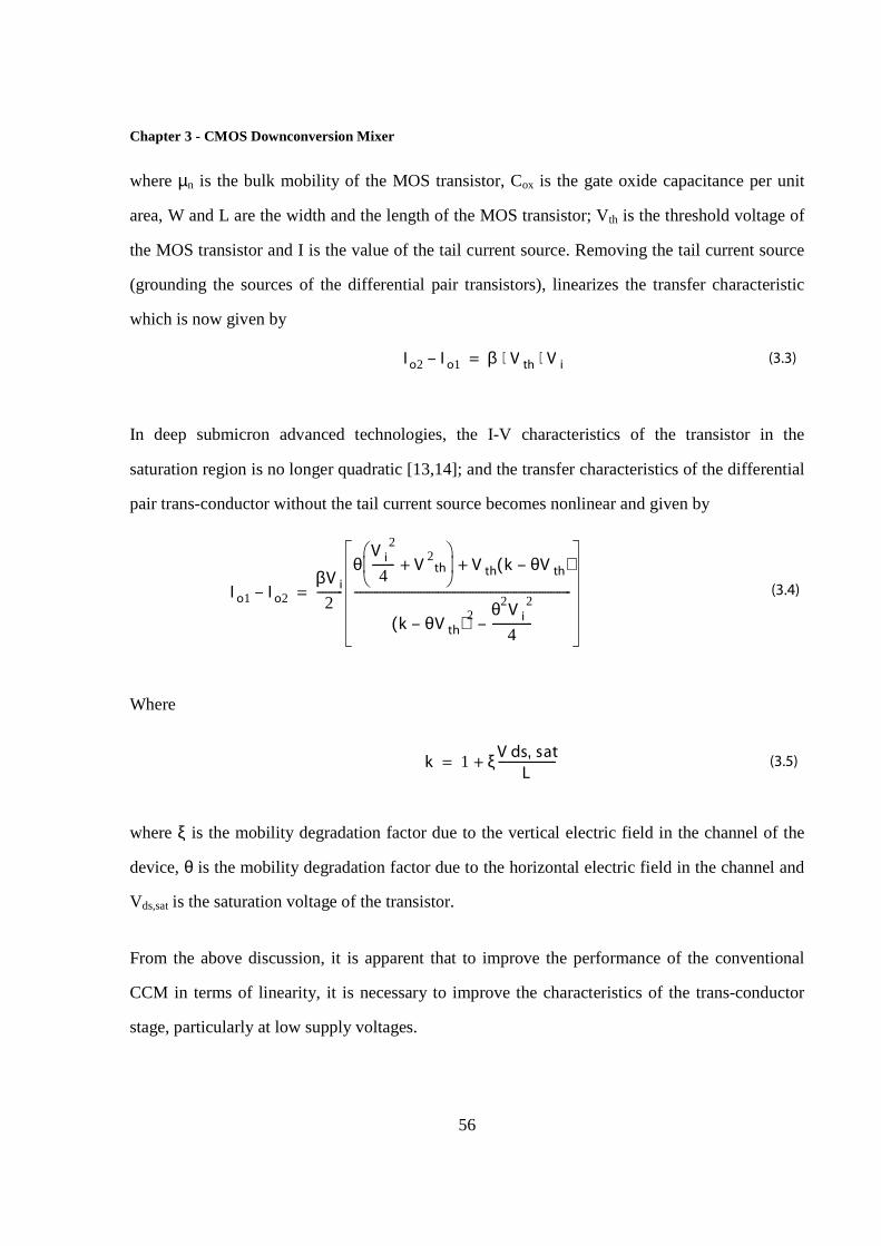
Chapter 3 - CMOS Downconversion Mixer
56
where µn is the bulk mobility of the MOS transistor, Cox is the gate oxide capacitance per unit
area, W and L are the width and the length of the MOS transistor; Vth is the threshold voltage of
the MOS transistor and I is the value of the tail current source. Removing the tail current source
(grounding the sources of the differential pair transistors), linearizes the transfer characteristic
which is now given by
Io2 I o1– β V th V i⋅ ⋅= (3.3)
In deep submicron advanced technologies, the I-V characteristics of the transistor in the
saturation region is no longer quadratic [13,14]; and the transfer characteristics of the differential
pair trans-conductor without the tail current source becomes nonlinear and given by
I o1 I o2–βV i
2---------
θV i
2
4-------- V
2th+
V th k θV th–( )+
k θV th–( )2 θ2V i
2
4--------------–
---------------------------------------------------------------------------= (3.4)
Where
k 1 ξV ds sat,L
--------------------+= (3.5)
where ξ is the mobility degradation factor due to the vertical electric field in the channel of the
device, θ is the mobility degradation factor due to the horizontal electric field in the channel and
Vds,sat is the saturation voltage of the transistor.
From the above discussion, it is apparent that to improve the performance of the conventional
CCM in terms of linearity, it is necessary to improve the characteristics of the trans-conductor
stage, particularly at low supply voltages.

Chapter 3 - CMOS Downconversion Mixer
57
3.5 Proposed Mixer and Design Methodology
3.5.1 Background
A trans-conductor which improves the linearity of differential pair CMOS trans-conductors was
proposed by Wang and Guggenbuhl [16] and is shown in Fig. 3.10. It features a bias-offset
technique which involves applying an offset to the biasing voltages of the transistors acting as
trans-conductors (M1, M2, M3 and M4) in order to generate a constant trans-conductance. The
offset bias is applied through transistors M5, M6, M7 and M8. These transistors are equally sized.
Since the DC current flowing through M5 and M6 (M7 and M8) are equal, the DC voltage Voffset
applied to the gate-source junction of M6 (M8) is copied to the gate-source of M5 (M7) and the
desired offset between the gate bias voltages of M1 and M3 (M2 and M4) is hereby created. The
technique, however, is not suitable at low voltages and for low power and high frequency
applications. For proper operation of the circuit, it is necessary for the ac signal at the gates of
M1 and M3 (M2 and M4) to be identical which may not necessarily be the case at high
frequencies. At low supply voltages, the linearity of the circuit degrades due to the large number
of stacked transistors. In addition, due to the large number of parallel paths, the architecture is
not suitable for low power designs. Furthermore, all the trans-conductor transistors are subject to
different threshold voltage modulation effects due to the unequal source and bulk voltages which
introduce nonlinearities.

Chapter 3 - CMOS Downconversion Mixer
58
Fig.3.10 The original form of the bias offset technique applied to a conventional NMOS differential pair (highlighted in bold lines) [16].
3.5.2 Novel Mixer Architecture
In this work, a new version of the bias offset technique is used in the trans-conductor design to
relax the trade-off between the power conversion gain and linearity while preserving the trans-
conductance gain of the circuit and operating at low supply voltages.
Fig.3.11(a) illustrates the novel trans-conductor architecture [17,18]. The offset voltage Voffset
provides a controlled bias between the gates of M1 and M2 (M3 and M4). In order to decrease the
power consumption of the circuit, current reuse [19,20] is employed in the design through the N
and P-channel common source transistors M1 and M2 (M3 and M4). This technique allows
doubling the trans-conductance gain for the same power consumption.

Chapter 3 - CMOS Downconversion Mixer
59
Fig.3.11 The proposed trans-conductor. (a) The bias-offset-technique applied to M1 and M2 (M3 and M4). (b) The circuit diagram of the proposed bias-offset technique.
In order to gain analytical insight into the linearization technique, the trans-conductance of the
circuit shown in Fig. 3.11(a) was derived using the following ID-VGS transfer characteristics for
the MOS transistors [21]
ID
µ°Cox
2 1 θ VGS
Vth
–( ) ξVDS sat,L
----------------------+ +
---------------------------------------------------------------------------------------W
L----- V
GSVth
–( )2⋅ ⋅= (3.6)
where µο is the low field bulk mobility of the carriers and VGS is the gate to source voltage of the
device. This equation preserves the required simplicity for hand calculations while taking into
account short channel effects which impact the linearity of the trans-conductance of the device.
The trans-conductance gm of a MOS transistor calculated from equation (3.6) is
gm
ID
∂
VGS
∂--------------- µ°Cox
W
L-----
VGS
Vth
–
1 2 θ ξL---+
VGS
Vth
–( )⋅+
---------------------------------------------------------------------⋅ ⋅≈= (3.7)
The trans-conductance Gm of the half circuit consisting of M1, M2 and the floating voltage source
Voffset in Fig. 3.11(a) is given by

Chapter 3 - CMOS Downconversion Mixer
60
Gm
Io1∂
Vinp
∂---------------
ID1 I
D2–( )∂
Vinp
∂---------------------------------
ID1∂
Vinp
∂---------------
ID2∂
Vinp
∂---------------–= = = (3.8)
where Vinp is the voltage applied to the input of the trans-conductor half circuit, as illustrated in
Fig. 3.11.
Since VSG1=VDD-V inp and VGS2=Vinp+Voffset, for a fixed VDD and Voffset, ∂V inp is given by
Vinp
∂ VSG 1∂– V
G S2∂= = (3.9)
From equations (3.8) and (3.9), Gm can be expressed in terms of the trans-conductances gm1 and
gm2 of transistors M1 and M2 as
Gm
gm1 g
m2+( )–= (3.10)
From equations (3.7) and (3.10), Gm can be obtained in terms of Voffset, Vinp and the aspect ratio
of transistors M1 and M2 as
Gm
C–ox
µon
W
L-----
2
Vinp
Voff set
Vthn
–+
1 2 θn
ξn
L 2------+
Vinp
Vof fset
Vthn
–+( )+
-----------------------------------------------------------------------------------------------------⋅ ⋅=
(3.11)Cox
µop
–W
L-----
1
Vdd
Vinp
– Vthp
–
1 2 θp
ξp
L 1------+
Vdd
Vinp
– Vthp
–( )+
-----------------------------------------------------------------------------------------------⋅ ⋅
To achieve a maximally flat (maximally constant) Gm as a function of Vinp at peak Gm, which
eventually results in a maximally linear trans-conductor, the second and third order derivatives of
Gm with respect to Vinp are set to zero at peak Gm by choosing a proper value for Voffset and
(W/L)2/(W/L)1. For typical values of the technology parameters, Fig. 3.12 is a normalized plot of
Gm without applying the flattening technique (plot with diamond markers), and with its second
and third order derivatives set to zero (plot with square markers).
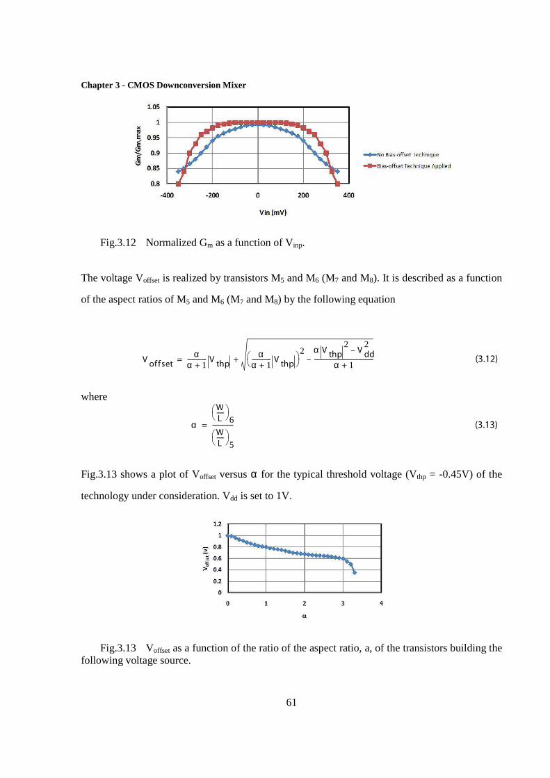
Chapter 3 - CMOS Downconversion Mixer
61
Fig.3.12 Normalized Gm as a function of Vinp.
The voltage Voffset is realized by transistors M5 and M6 (M7 and M8). It is described as a function
of the aspect ratios of M5 and M6 (M7 and M8) by the following equation
Vof fset
αα 1+------------- V
thpα
α 1+------------- V
thp
2 α Vthp
2Vdd2
–
α 1+----------------------------------------–+= (3.12)
where
α
W
L-----
6W
L-----
5
--------------= (3.13)
Fig.3.13 shows a plot of Voffset versus α for the typical threshold voltage (Vthp = -0.45V) of the
technology under consideration. Vdd is set to 1V.
Fig.3.13 Voffset as a function of the ratio of the aspect ratio, a, of the transistors building the following voltage source.

Chapter 3 - CMOS Downconversion Mixer
62
The low-voltage capability of the trans-conductor shown in Fig.3.11(b) is achieved by offsetting
the gate bias voltage of M1 and M2 (M3 and M4) to provide simultaneously high input voltage
range for both M1 and M2 (M3 and M4) at a supply voltage of 1V. The design ensures
simultaneous operation of M1, M2, M3 and M4 in the active region over a relatively large range of
the input signal levels. This feature along with the fully symmetric characteristics of the design is
key to the good linearity behaviour of the design in terms of second-order nonlinearity. Capacitor
C1 in Fig. 3.11(b) provides a feed forward path for the RF signal and improves the high
frequency performance of the floating voltage source. By introducing C1, the RF signal
appearing at the gates of M1 and M2 (M3 and M4) will be identical as required for the proper
operation of the circuit. This form of the bias offset technique is applicable at any RF frequency
as long as the transistor is capable of providing a reasonable trans-conductance. In order to
further improve the linearity of the trans-conductor, threshold voltage modulation is eliminated
by shorting the source-bulk junctions of all the transistors used in the stage. The Deep-N-Well
(DNW) non-linear capacitor is choked by adding a 10kΩ resistor in DNW ties to the power
supply (soft tied DNW).
Fig. 3.14 illustrates the simulated trans-conductance Gm of the half circuit shown in Fig.3.11(b)
and consisting of M1, M2, M5 and M6 for three different values of Voffset and for
(W/L)1=32µm/0.18µm and (W/L)2=20µm/0.18µm. As observed, a value of Voffset=750mV
results in a constant trans-conductance over a relatively wide range of the input differential
voltage (-280mV to 280mV), which in turn translates into good linearity performance of the
mixer.

Chapter 3 - CMOS Downconversion Mixer
63
Fig.3.14 Trans-conductance Gm of the trans-conductor, for three different values of offset voltage. The flat trans-conductance (Voffset=750mV) was obtained for (W/L)1=32µm/0.18µm, (W/L)2=20µm/0.18µm, (W/L)5=30µm/0.25µm, (W/L)6=16µm/0.18µm.
The final schematic of the mixer under consideration is illustrated in Fig. 3.15 and the values of
all the components are given in the caption. As illustrated, the RF trans-conductor is ac-coupled
to a mixing stage made of cross-coupled differential pairs which is terminated in a low pass load
to eliminate any undesirable high frequency content in the output signal. Active loads are
avoided at the output of the mixer to minimize flicker noise and improve the NF at baseband
frequencies. The cross coupled mixing stage is biased through LC resonators (set at 8 GHz)
instead of the conventional current sources to enable low-voltage operation [22] and optimize the
performance of the mixing stage at 8GHz.
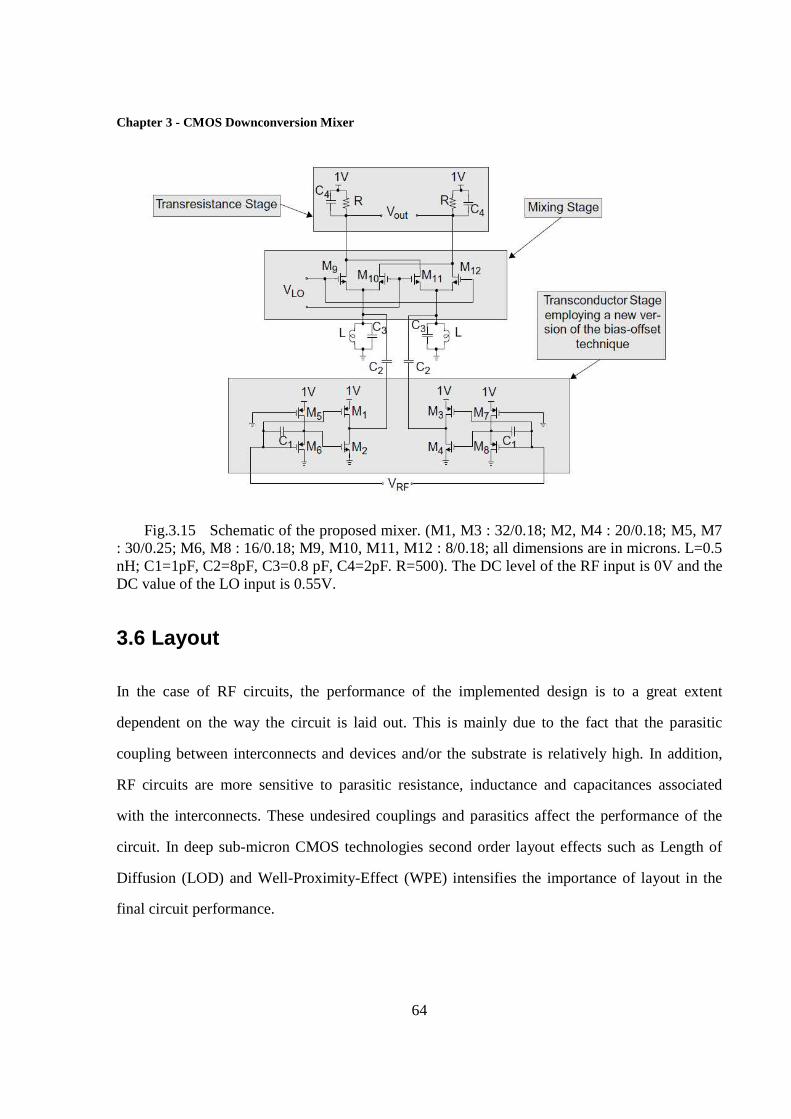
Chapter 3 - CMOS Downconversion Mixer
64
Fig.3.15 Schematic of the proposed mixer. (M1, M3 : 32/0.18; M2, M4 : 20/0.18; M5, M7 : 30/0.25; M6, M8 : 16/0.18; M9, M10, M11, M12 : 8/0.18; all dimensions are in microns. L=0.5 nH; C1=1pF, C2=8pF, C3=0.8 pF, C4=2pF. R=500). The DC level of the RF input is 0V and the DC value of the LO input is 0.55V.
3.6 Layout
In the case of RF circuits, the performance of the implemented design is to a great extent
dependent on the way the circuit is laid out. This is mainly due to the fact that the parasitic
coupling between interconnects and devices and/or the substrate is relatively high. In addition,
RF circuits are more sensitive to parasitic resistance, inductance and capacitances associated
with the interconnects. These undesired couplings and parasitics affect the performance of the
circuit. In deep sub-micron CMOS technologies second order layout effects such as Length of
Diffusion (LOD) and Well-Proximity-Effect (WPE) intensifies the importance of layout in the
final circuit performance.
Chapter 3 - CMOS Downconversion Mixer
65
3.6.1 High Frequency Layout Considerations
In this work, the substrate is covered with the lowest layer of metal as a ground plane where
possible, to shield it from the noise coming from the high frequency interconnects and pads.
All transistor gates are connected at both ends to reduce gate resistance. Guard rings are placed
around the transistors to reduce the equivalent substrate resistance and to lower noise injection to
the substrate. Dummy diffusions and fingers are placed where applicable to achieve predictable
and matched device performance. Also, a large number of contacts and vias are used to decrease
interconnect resistance. The finger width in the transistor layout is chosen such that the
transistor’s noise and speed performance are optimized (in this case, a finger width of 2.5µm
results in optimal performance for noise).
To improve the RF-port to LO-port isolation, the separation between the RF and the LO sections
of the mixer is maximized in addition to placing all transistors individually in DNWs isolated
from the substrate to minimize coupling between the two ports. The mixing cross-coupled
transistors are placed in one DNW as a group to minimize parasitic capacitance.
3.6.2 Layout Considerations for Best Linearity Performance
The second order nonlinearities in a CMOS differential design can be affected by any asymmetry
or systematic mismatch in the differential paths. Therefore, it is important for the layout to be
fully symmetric to maximize the differential signal paths matching. The symmetry of the layout
also helps in rejecting the common noise picked up by the circuit from other devices located on
the same chip.
Undesired threshold voltage modulation due to the body effect is one of the factors affecting the
linearity characteristics of MOS transistors. It can be eliminated by shorting the source and the

Chapter 3 - CMOS Downconversion Mixer
66
bulk of the transistors and surrounding each transistor with sufficient bulk contacts shorted to the
source. In doing so, the DNW where the device resides is soft-tied to VDD to minimize the non-
linear effect of the DNW parasitic diode. Fig. 3.16 illustrates the layout considerations used to
eliminate the threshold voltage modulation assisted nonlinearity for N-channel MOS transistors.
A similar approach may be used to eliminate the body effect of the P-channel MOS transistor.
Fig.3.16 Layout consideration to achieve best linearity performance.
3.6.3 Mixer Layout
The mixer was designed in a standard 0.18 µm CMOS technology with six layer of metallization.
The layout of the mixer is illustrated in Fig. 3.17. The core area of the design is 320 x 400 µm2.
The test chip area including the pads is 1080 x 710 µm2. Decoupling capacitors (100 pF) were
used on-chip at VDD. All capacitors are implemented using metal-insulator-metal (MIM)
integrated capacitors. The resistors are implemented using un-silicided poly-silicon resistors
sitting on a deep-NWELL soft tied to VDD.

Chapter 3 - CMOS Downconversion Mixer
67
Fig.3.17 The proposed mixer layout.
The inductors were implemented as spirals using the sixth metal layer. They were designed using
Agilent Technologies Advanced Design System (ADS) software package [23]. The layout of a
typical 0.5nH inductor is shown in Fig. 3.18. The dimensions of the inductor are displayed in the
diagram.
Fig.3.18 0.5nH integrated inductor aspect ratio.
For post layout simulations, the inductors were replaced by a lumped model at 8 GHz, obtained
using ADS and shown in Fig. 3.19.

Chapter 3 - CMOS Downconversion Mixer
68
Fig.3.19 Integrated inductor lumped model used for post layout simulation.
3.7 Post-Layout Simulations
The simulations of the mixer were carried out using the Spectre simulator [24]. Fig. 3.20
illustrates the two-tone test post-layout simulation results at 8001MHz and 8003MHz. The
intercept of the linear extrapolation of the first and third order terms indicates an IIP3 of +3 dBm.
The IIP2 of the mixer was simulated and found to be better than +52 dBm using Monte-Carlo
simulation. The linearity characterization was carried out using time domain simulations and
taking the Discrete Fourier transform (DFT) of the output waveform to find the power of the
linear and intermodulation tones present in the output spectrum.
Fig. 3.21 shows a plot of the power transfer characteristics of the mixer. From the plot, it is
apparent that the mixer exhibits a 1-dB compression point of -8 dBm and a power conversion
gain (PCG) of +10 dB.

Chapter 3 - CMOS Downconversion Mixer
69
Fig.3.20 Two-tone simulation.
Fig.3.21 Power transfer characteristics of the mixer.
The noise figure simulation for the mixer reveals a minimum noise figure of 10dB.

Chapter 3 - CMOS Downconversion Mixer
70
Table 3.1 compares the post layout simulation results to the target specifications listed in Chapter
1. As observed, the proposed mixer meets the low-voltage and linearity requirements of future
generations of mobile phones. Specifically, the design relaxes the trade-off between power
conversion gain and linearity of CCMs which allows for simultaneously improving the gain and
linearity of the mixer. The design offers considerable advantages over the conventional CCM [5]
in terms of gain and linearity and in addition operates at 1 V supply which is not possible in the
conventional case.
Table 3.1 Target Specifications and Post Layout Simulations
Target
specifications
Simulation Results; Typical Process
Parameters, 25oC
Technology (mm) 0.18 0.18
Supply Voltage (v) 1 1
Frequency (GHz) 8 8
Noise Figure (dB) <13 10
IIP3(dBm) > 3 +3
IIP2 (dBm) > 50 +52
P-1dB (dBm) > -7 -8
Conversion Gain (dB) > 6 + 10
Power Consumption (mW)
Minimum 6.2
Table 3.2 shows the effect of process variation on the performance of the proposed mixer
architecture. The speed worst case and power worst case listed in the Table include power supply
variations of +10% and -10% respectively. The Table confirms the robustness of the design to
process and supply voltage variations.
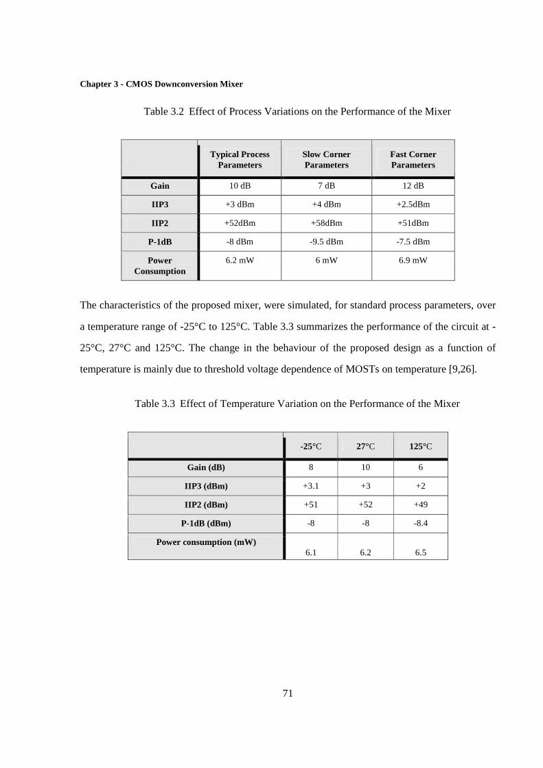
Chapter 3 - CMOS Downconversion Mixer
71
Table 3.2 Effect of Process Variations on the Performance of the Mixer
Typical Process
Parameters Slow Corner Parameters
Fast Corner Parameters
Gain 10 dB 7 dB 12 dB
IIP3 +3 dBm +4 dBm +2.5dBm
IIP2 +52dBm +58dBm +51dBm
P-1dB -8 dBm -9.5 dBm -7.5 dBm
Power Consumption
6.2 mW 6 mW 6.9 mW
The characteristics of the proposed mixer, were simulated, for standard process parameters, over
a temperature range of -25°C to 125°C. Table 3.3 summarizes the performance of the circuit at -
25°C, 27°C and 125°C. The change in the behaviour of the proposed design as a function of
temperature is mainly due to threshold voltage dependence of MOSTs on temperature [9,26].
Table 3.3 Effect of Temperature Variation on the Performance of the Mixer
-25°C 27°C 125°C
Gain (dB) 8 10 6
IIP3 (dBm) +3.1 +3 +2
IIP2 (dBm) +51 +52 +49
P-1dB (dBm) -8 -8 -8.4
Power consumption (mW) 6.1
6.2
6.5

Chapter 3 - CMOS Downconversion Mixer
72
3.8 Summary
The current commutating mixer (CCM) and the three main blocks involved in the architecture of
CCM were discussed. The various linearization techniques previously applied to the CCM were
presented and the limitations of each of those techniques were considered. A novel CCM
architecture using a bias offset technique was proposed. This architecture relaxes the inherent
trade-off between power conversion gain and linearity that governs all type of active mixers. The
post-layout simulation results indicate that the proposed design satisfies the linearity, low voltage
and design simplicity requirements of future generations of mobile phones.

Chapter 3 - CMOS Downconversion Mixer
73
References
[1] E. Terrovitis and R. G. Meyer, “Intermodulation Distortion in Current Commutating CMOS Mixers,” IEEE Journal of Solid-State Circuits, Vol. 35, pp. 1461 - 1473, 2000.
[2] H. Kilicasian, H. S. Kim and M. Ismail, “A 1.9 GHz CMOS RF Down-Conversion Mixer,” Proceedings of the 40th Midwest Symposium on Circuits and Systems, Vol. 2, pp. 1172 - 1174, 1997.
[3] J. Harvey and R. Harjani, “An Integrated Quadrature Mixer with Improved Image Rejection at Low Voltage,” 14th International Conference on VLSI Design, pp. 269 - 273, 2001.
[4] J. Jussila and K. Halonen, “Calibration Techniques of Active BICMOS Mixers,” IEEE Journal of Solid-State Circuits, Vol. 37, pp. 766 - 769, 2002.
[5] Q. Li, J. Zhang, W. Li and J. S. Yuan, “CMOS RF Mixer Non-Linearity Design,” IEEE 43rd Midwest symposium on Circuits and Systems, pp. 808 - 811, 2001.
[6] E.E. Bautista, B. Bastani and J. Heck, “A High IIP2 Downconversion Mixer Using Dynamic Matching,” IEEE Journal of Solid-State Circuits, Vol. 35, pp. 1934 - 1941, 2000.
[7] O. Mitrea, C. Popa, A. M. Manolescu and M. Glesner, “A Linearization Technique for Ra-dio Frequency CMOS Gilbert-Type Mixers,” Proceedings of the 10th IEEE International Conference on Electronics, Circuits and Systems, Vol. 3, pp. 1086 - 1089, 2003.
[8] R. F. Salem, S. H. Galal, M. S. Tawfik and H. F. Ragaie, “A New Highly Linear CMOS Mixer Suitable for Deep Submicron Technologies,” Proceedings of the 9th IEEE Interna-tional Conference on Electronics, Circuits and Systems, Vol. 1, pp. 81 - 84, 2002.
[9] H. C. Wei, R. M. Weng and K. Y. Lin, “A 1.5 V High-Linearity CMOS Mixer for 2.4 GHz Applications,” Proceedings of the International Symposium on Circuits and Systems, Vol. 1, pp. I-561 - I-564, 2004.
[10] P. R. Gray and R. G. Meyer, “Analysis and Design of Analog Integrated Circuits,” Second Edition, John Wiley & Sons, pp. 183, 1984.
[11] T. H. Lee, “The Design of CMOS Radio Frequency Integrated Circuits,” Cambridge Uni-versity Press, 2001.
[12] S. Szczepanski, R. Schaumann and P. Wu, “Linear Transconductor Based on Crosscoupled CMOS Pairs,” Electronics Letters, Vol. 27, pp. 783 - 785, 1991.
[13] P. E. Allen and D. R. Holberg, CMOS Analog Circuit Design, Fort Worth, TX: Holt, Rine-hart and Winston, pp. 490 - 497, 1987.
[14] F. Babarada, M. D. Profirescu and A. Rusu, “MOSFET Mobility Degradation Modelling,” IEEE International Semiconductor Conference, Vol. 2, pp. 301 - 304, 2003.
[15] E. Terrovidis, “Analysis and Design of Current-Commutating CMOS Mixers,” Ph.D. Disser-tation, University of California at Berkeley, Chapter 7, PP. 174, 2001.

Chapter 3 - CMOS Downconversion Mixer
74
[16] Z. Wang and W. Guggenbuhl, “A Voltage-Controllable Linear MOS Transconductor Using Bias Offset Technique,” IEEE Journal of Solid-State Circuits, Vol. 25, pp. 315 - 317, 1990.
[17] F. Mahmoudi and C.A.T. Salama, “Low-Voltage, Low-Power, High Linearity, Active CMOS Mixer,” US Patent, Publication # 2005-0124311-A1.
[18] F. Mahmoudi and C. A. T. Salama, “8 GHz, 1V, High Linearity, Low Power CMOS Active Mixer,” IEEE Radio Frequency Integrated Circuit Symposium, pp. 401 - 404, 2004.
[19] T. Tsukahara, M. Harada, M. Ugajin, J. Kodate and A. Yamagishi, “Design Methodology of Low-Power CMOS RF-ICs,” Proceedings of the Asia and South Pacific Design Automation Conference, ASP-DAC, PP. 394 - 399, 2003.
[20] A. N. Karanicolas, “A 2.7V 900 MHz CMOS LNA and Mixer,” IEEE Journal of Solid-State Circuits, Vol. 31, pp. 1939 - 1944, 1996.
[21] P. Antognetti and G. Massobrio, “Semiconductor Device Modeling with SPICE,” Mc Graw-Hill, 1992.
[22] T. Manku, “Low Voltage Topology for Radio Frequency Circuit Design,” US-Patent #6,232,848, 2001.
[23] Agilent Technologies Advanced Design System, Available: http://www.agilent.com
[24] Virtuoso Spectre Circuit Simulator, Available: http://www.cadence.com/products/custom_ic/spectre.
[25] F. Carr and P. Vorenkamp, “System and Method for Providing a Low Power Receiver De-sign,” US Patent Application # 20010008430, 2001.
[26] V. Krizhanovskii, N. T. Kien and S. G. Lee, “0.18 mm CMOS LNA and Mixer for Wireless LAN Applications,” IEEE 12th International Conference on Microwave and Telecommuni-cation Technology, pp. 137-138, 2002.

Chapter 4 - CMOS Quadrature Generator
75
CHAPTER 4: CMOS Quadrature Generator
4.1 Introduction
This chapter deals with the design and analysis of the 8 GHz quadrature generator. The design
embodies the quadrature generation scheme into the LO-buffer using active inductors. The
layout and post layout simulations of the proposed design are presented.
4.2 Conventional Quadrature Generators
Signals with equal amplitudes and quadrature phases are widely used in a variety of applications
including direct conversion receivers to demodulate the incoming angle-modulated data.
Previously reported quadrature generators and their pros and cons were discussed in Chapter 1.
As mentioned in that chapter, the necessity for buffering stages between the local oscillator and
the quadrature generator as well as between the quadrature generator and the mixers in
previously reported quadrature generators, increases the power consumption. To decrease the
power consumption, these buffers should be eliminated.
The concept of integrating the quadrature generating scheme into the LO-buffer was previously
introduced by Steyaert and Roovers [1] using bipolar technology. A CMOS implementation of
the design is illustrated in Fig. 4.1.

Chapter 4 - CMOS Quadrature Generator
76
Fig 4.1 Quadrature generation components imbedded in the LO buffer [1].
In this circuit, the differential input voltages denoted as VLOn and VLOp in the figure are
transformed to current by the capacitive and resistive degenerated differential pairs, resulting in iI
and iQ given by
i I V L Op V L On–( ) sC⋅= (4.1)
iQV L Op V L On–
R--------------------------------= (4.2)
As observed from equations (4.1) and (4.2), iI and iQ exhibit a phase difference of 90°. The
resistive loads RL transform the currents iI and iQ to voltages while preserving the 90° phase shift
resulting in the four quadrature phase outputs, VIp, VIn, VQp and VQn defined as

Chapter 4 - CMOS Quadrature Generator
77
V I p R L V L op V L on–( ) sC⋅–= (4.3)
V I n R L V L op V L on–( ) sC⋅= (4.4)
V Qp R L
V L op V L on–( )R
-----------------------------------–= (4.5)
V Qn R L
V L op V L on–( )R
-----------------------------------= (4.6)
The magnitudes of the four outputs in equations (4.3) to (4.6) are equal only at one frequency.
This frequency is obtained by equating the magnitudes of the four outputs which results in
R L V L op V L on–( ) sC⋅ R L
V L op V L on–( )R
---------------------------------= (4.7)
and implies that |s| = |jω| = ω = 1/RC. This technique provides a 90° phase difference between
the outputs of the capacitive and resistive degenerated sections of the circuit only if the quality
factor of the capacitor is infinite.
Although the design achieves relatively low power consumption by eliminating the buffers
located between the quadrature generator and the mixers, in a CMOS implementation, it tends to
cause instability due to the negative real part at the gate of the input transistors (M1 and M2)
generated by the capacitance used for capacitive degeneration (capacitor C in Fig. 4.1) [2].
The focus of this chapter is to present a design scheme that eliminates the buffer between the
quadrature generator and the mixers, and integrates the quadrature generation circuitry into the
local-oscillator buffer.

Chapter 4 - CMOS Quadrature Generator
78
4.3 Novel Quadrature Generator Architecture
The block diagram of the proposed design is illustrated in Fig.4.2 [3]. It consists of a LO-buffer,
a differential active inductor and two common-mode stabilizers. In this architecture, there is no
need for isolating the quadrature generator from the mixers by using additional buffers, since the
capacitive loading of the mixers on the quadrature generator can be used in the active inductor
design. The LO-buffer consists of common source n-channel transistors loaded by p-channel
transistors. The differential active inductor is illustrated in Fig.4.3 and is based on the
conventional Gm-C structure. The value of the inductance in this architecture is given by [4]
LC t
gmi g′mi⋅----------------------= (4.8)
where gmi and gmi are the trans-conductances of M7 (M8) and M5 (M6) respectively and Ct is the
total differential parasitic capacitance at the input of the trans-conductor blocks. The capacitive
loading of the mixers on the quadrature generator shown in Fig. 4.2 contribute to the capacitance
Ct.
Fig 4.2 Block diagram of the quadrature generator under consideration.
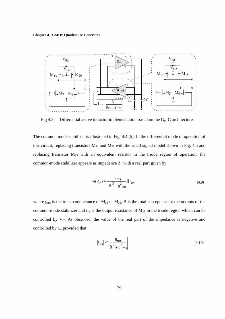
Chapter 4 - CMOS Quadrature Generator
79
Fig 4.3 Differential active inductor implementation based on the Gm-C architecture.
The common mode stabilizer is illustrated in Fig. 4.4 [5]. In the differential mode of operation of
this circuit, replacing transistors M21 and M22 with the small signal model shown in Fig. 4.5 and
replacing transistor M23 with an equivalent resistor in the triode region of operation, the
common-mode stabilizer appears as impedance Zo with a real part given by
R e Zo
gms
B2
g2
+ ms
--------------------------- ros
||–≈ (4.9)
where gms is the trans-conductance of M21 or M22, B is the total susceptance at the outputs of the
common-mode stabilizer and ros is the output resistance of M23 in the triode region which can be
controlled by VC. As observed, the value of the real part of the impedance is negative and
controlled by ros provided that
ros
gms
B2
g2
+ ms
---------------------------> (4.10)

Chapter 4 - CMOS Quadrature Generator
80
Fig 4.4 Common mode stabilizer circuit.
Fig 4.5 Small signal model of the MOS transistor in the active region of operation.
4.4 Design and Analysis of the Proposed Quadrature
Generator
The complete circuit of the proposed quadrature generator is shown in Fig.4.6. Transistors M1,
M2, M13 and M14 form the LO-buffer and M3, M4, M19 and M20 are dummy transistors identical
to M1, M2, M13 and M14, added to the circuit to preserve the symmetry of the circuit, which is
crucial for proper quadrature operation. The capacitors Caux implemented by the gate to source
and gate to drain capacitances of the n-channel transistors M9, M10, M11 and M12, are included in
the design to relax the coupling between the amplitude and phase tuning of the quadrature
generator by cancelling out the gate to drain capacitances of transistors M1, M2 (M3, M4). This is
done by setting the aspect ratio (W/L) of M9 to M12 to be half of that of M1 to M4 such that the
sum of the gate to drain and the gate to source capacitances of M9 to M12 equals the gate to drain
capacitance of M1 to M4. To obtain analytical insight into the quadrature signal generation of the
circuit, the outputs of the circuit of Fig.4.6 are derived in terms of the differential local oscillator
voltage (VLO). This is done by replacing transistors M1, M2 and M5 to M8 by the small signal
model illustrated in Fig.4.5 and replacing transistors M3, M4 and M13 to M20 by parallel RC
circuits, representing the output resistance and the sum of the drain to bulk and drain to gate
capacitances of each transistor. In the differential mode of operation, the common-mode

Chapter 4 - CMOS Quadrature Generator
81
stabilizers are replaced by a negative resistance which is designed to cancel out the equivalent
conductance at nodes A, B, C and D in Fig.4.6, which is necessary for the quadrature phase
matching of the outputs. The output capacitance of the common-mode stabilizer is merged in the
equivalent capacitances at nodes A, B, C and D. The resulting equations specifying voltages V1
to V4 are listed below:
Fig 4.6 Circuit of the quadrature generator. (M1 to M8 : 10/0.18; M21, M22, M24 and M25: 9/0.18; M13, M14, M19 and M20 : 12/0.18; M9 to M12 : 5/0.18; M15 to M18 : 12/0.18; M23 and M26 are zero threshold voltage devices: 6/0.5; all dimensions are in µm. Vdd=1V, VB=750mV, VB1=150mV, VB2=0, VC=850mV)
Chapter 4 - CMOS Quadrature Generator
82
(4.1 1)V 1 H s( ) gmb
s Caux
Cgdb
–( )+[ ] goeq
s 2Cgdi
Cgdb
Ceq
Caux
+ + +( )+[ ]VL O
=
V 2 H s( ) gmb
s Caux
Cgdb
–( )+[ ]gmi
VL O
= (4.12)
V 3 H s( ) gmb
s Caux
Cgdb
–( )+[ ]gmi
VL O
–= (4.13)
(4.14)V 4 H– s( ) gmb
s Caux
Cgdb
–( )+[ ] goeq
s 2Cgdi
Cgdb
Ceq
Caux
+ + +( )+[ ]VL O
=
where
(4.15)H s( )gmi
2sCgdi
–( )2 goeq
s 2Cgdi
Cgdb
Ceq
Caux
+ + +( )+[ ]2–
a s( ) b s( )–------------------------------------------------------------------------------------------------------------------------------------------------------------=
and
a s( ) goeq
s 2Cgdi
Cgdb
Ceq
Caux
+ + +( )+( )2 2Cgdi
gmi
sCgdi
–( )+2
= (4.16)
b s( ) s2C
2gdi g
misC
gdi–( )2+
2= (4.17)
where Cgdb is the gate to drain capacitance of the n-channel transistors in the LO-buffer, Cgdi
represents the gate to drain capacitor of the n-channel transistors forming the active inductor, Ceq
is the equivalent capacitance at nodes A, B, C and D, gmb is the transconductance of the n-
channel transistors in the LO-buffer, gmi is the transconductance of the n-channel transistors in
the active inductor and goeq is the equivalent conductance at nodes A, B, C and D.
As observed from equations (4.11) to (4.14), by eliminating the equivalent conductance at nodes
A, B, C and D in Fig.4.6 (i.e. goeq=0), using the negative output conductance of the common-

Chapter 4 - CMOS Quadrature Generator
83
mode stabilizer circuit in its differential mode of operation, the voltages V1 and V4 have a 90°
phase shift relative to V2 and V3 respectively. This phase shift is represented by the term
s(2Cgdi+Cgdb+Ceq+Caux) in the analytical expressions for V1 and V4. Vc can also be used to apply
an optional automatic phase tuning signal to this circuit to compensate for process and
temperature variations of the output phase [6]. From equations (4.11) to (4.14) it is clear that
once the quadrature phase matching is achieved (goeq=0), the amplitudes of V1 to V4 can be made
equal at a desired frequency, provided that
gmi
ω 2Cgdi
Cgdb
Ceq
Caux
+ + +( )⋅= (4.18)
The value of gmi is adjusted by setting the DC currents of M5 to M8 using the p-channel transistor
M15 to M18 in Fig. 4.6 to satisfy equation (4.18).
By choosing Caux=Cgdb, the multiplicand [gmb + s(Caux-Cgdb)] in equations (4.11) to (4.14),
reduces to gmb, and therefore the magnitudes of V1, V2, V3 and V4 can be adjusted independently
of their phases by varying gmb. The trans-conductance gmb is controlled by the bias current
flowing through M1 and M2 using the p-channel transistors M13 and M14 and VB1. An optional
automatic amplitude control signal VB1 can be applied to the gates of M13 and M14 to compensate
for process and temperature variations of the output amplitudes [5].
The common-mode equivalent half-circuit of the quadrature generator illustrated in Fig. 4.6 is
shown in Fig. 4.7. The auxiliary capacitors are not included in this Figure. In the common mode
of operation, they are absorbed in the gate-drain capacitances of the n-channel transistors in the
LO-buffer. In order to explain how the common mode stabilizer stabilizes the proposed circuit,
the common mode transfer function of the circuit is extracted for two different cases: one
excluding the common mode stabilizer transistors (M21 and M24) and one including them. These
two cases are discussed in details below.

Chapter 4 - CMOS Quadrature Generator
84
Fig 4.7 Equivalent common mode half circuit of the proposed quadrature generator.
The common mode transfer function of the quadrature generator without the common mode
stabilizer transistors M21 and M24 is obtained from the common mode equivalent circuit
illustrated in Fig. 4.7, by replacing transistors M1, M5, M7 with their small signal model, and
replacing the rest of the transistors with their parasitic resistances and capacitances and is given
by
V o
V L O
----------gm1 sCgd1–( ) g2 s C 2 C 3+( )+( )
qs2
rs g1g2 gm5gm7–+ +------------------------------------------------------------------------------= (4.19)
Where
q C 3 C 1 C2 C gd1+ +( ) C 2 C 1 C gd1+( )+= (4.20)
r g1 C 2 C 3+( ) g2 C 1 C 2 C gd1+ +( ) C 2 gm5 gm7+( )+ += (4.21)
C 1 C o7 C o13 C+o15 Co1 C+
gs5+ += (4.22)

Chapter 4 - CMOS Quadrature Generator
85
C 2 C gd7 C gd5+= (4.23)
C 2 C gd7 C gd5+= (4.24)
C 3 C o3 C+o5 Co17 C o19 C gs7+ + += (4.25)
g1 go1 go7 go13 go15+ + += (4.26)
g2 go3 go5 go17 go19+ + += (4.27)
and Co1, Co3, Co5, Co7, Co13, Co15, Co17 and Co19 are the total capacitance seen at the drain of M1,
M3, M5, M7, M13, M15, M17 and M19 respectively; go1, go3, go5, go7, go13, go15, go17 and go19 are the
output conductance of M1, M3, M5, M7, M13, M15, M17 and M19 respectively and Cgd1, Cgd5 and
Cgd7 are the gate-drain capacitances of M1, M5 and M7 respectively.
The denominator of the common mode transfer function in equation (4.19) is a second order
polynomial where q and r have positive values. The term (g1g2-gm5gm7) is negative since the
trans-conductances gm3 and gm5 typically have a greater value than the output conductances g1
and g2 of MOS transistors in the active region of operation. The signs of the three coefficients q,
r and (g1g2-gm5gm7) in the denominator of equation (4.19) imply that, in the common mode of
operation, the circuit has two poles, one located in the left half plane and the other located in the
right half plane. The common mode pole located on the right half plane results in the common
mode instability of the circuit. To solve this problem, the common mode stabilizer depicted in
Fig. 4.4 is added to the design.
The common mode transfer function of the quadrature generator including the common mode
stabilizer is given by
V o
V L O
----------gm1 sC gd1–( ) g2 gms s C 2 C 3+( )+ +( )
qs2
r ′s g1 gms+( ) g2 gms+( ) gm3gm5–+ +-------------------------------------------------------------------------------------------------------= (4.28)
Chapter 4 - CMOS Quadrature Generator
86
Where
r ′ g1 gms+( ) C 2 C 3+( ) g2 gms+( ) C 1 C 2 C gd1+ +( ) C 2 gm3 gm5+( )+ += (4.29)
By properly choosing the trans-conductance of transistors M21 and M24 (i.e. gms) the term
[(g1+gms)(g2+gms)-gm3gm5] will be positive and therefore all three coefficients in the denominator
of equation (4.28) (q, r´ and [(g1+gms)(g2+gms)-gm3gm5]) are positive which means both roots of
the second order polynomial in the denominator of equation (4.28) are in the left half plane
guarantying the common mode stability of the circuit.
In summary, the common mode stabilizer of Fig. 4.4 is designed such that in the differential
mode of operation the equivalent resistance of transistor M23 is used to adjust the quadrature
phase of the four outputs. In the common mode of operation, the trans-conductance of transistors
M21 and M22 (i.e. gms) moves the common mode poles of the quadrature generator to the left half
plane and thereby stabilizes the common mode behaviour of the circuit.
4.5 Layout of the Quadrature Generator
The core area of the quadrature generator layout is 150 x 90 µm2. The total area of the test chip
including the testing pads and decoupling capacitors is 1100 x 700 µm2. Decoupling capacitors
were used to bypass the supply and control voltage nodes to ground and hereby eliminate high
frequency noise picked up by the DC lines and interconnects. All n-channel transistors are placed
in deep n-wells to minimize the crosstalk between them thought the substrate. Accordingly, p-
channel transistors are located in separate n-wells. The finger widths of the transistors were
chosen to be 2.5 µm for optimum speed and noise performance. Perfect layout symmetry is
crucial for good circuit performance.
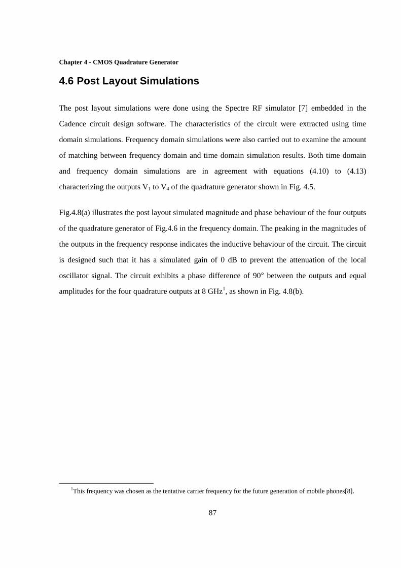
Chapter 4 - CMOS Quadrature Generator
87
4.6 Post Layout Simulations
The post layout simulations were done using the Spectre RF simulator [7] embedded in the
Cadence circuit design software. The characteristics of the circuit were extracted using time
domain simulations. Frequency domain simulations were also carried out to examine the amount
of matching between frequency domain and time domain simulation results. Both time domain
and frequency domain simulations are in agreement with equations (4.10) to (4.13)
characterizing the outputs V1 to V4 of the quadrature generator shown in Fig. 4.5.
Fig.4.8(a) illustrates the post layout simulated magnitude and phase behaviour of the four outputs
of the quadrature generator of Fig.4.6 in the frequency domain. The peaking in the magnitudes of
the outputs in the frequency response indicates the inductive behaviour of the circuit. The circuit
is designed such that it has a simulated gain of 0 dB to prevent the attenuation of the local
oscillator signal. The circuit exhibits a phase difference of 90° between the outputs and equal
amplitudes for the four quadrature outputs at 8 GHz1, as shown in Fig. 4.8(b).
1This frequency was chosen as the tentative carrier frequency for the future generation of mobile phones[8].

Chapter 4 - CMOS Quadrature Generator
88
Fig 4.8 Post layout simulation characteristics of the quadrature generator. (a) The magnitude and phase of the transfer function of the four outputs. (b) The time domain quadrature outputs.
Fig. 4.9 shows the simulated quadrature phase and amplitude matching of the design for a peak-
to-peak differential local oscillator input of 300 mV over a bandwidth of 100 MHz [9]. The
circuit illustrates a quadrature phase and amplitude matching of less than 1° and 0.4 dB
respectively for the typical device parameters over the bandwidth of interest. The output
quadrature phase and amplitude mismatch for the process corners were observed to be less than
6° and 1.5 dB respectively without applying any tuning.

Chapter 4 - CMOS Quadrature Generator
89
(a)
(b)
Fig 4.9 Simulation results of the quadrature generator. (a) Quadrature phase error. (b) Amplitude mismatch.
The variation in the control voltage required to compensate for process and supply voltage
variations under worst case process corners and a power supply voltage variation of +10% and -
10%, is less than 200mV. This control voltage can be generated by automatic amplitude and
phase tuning circuitry previously reported in the literature [6].
Table 4.1 compares the post layout simulation results of the quadrature generator to the target
specifications as listed in Table 1.2 in Chapter 1. As observed from the Table, the post layout
simulation results meet the target specifications of the quadrature generator under consideration.
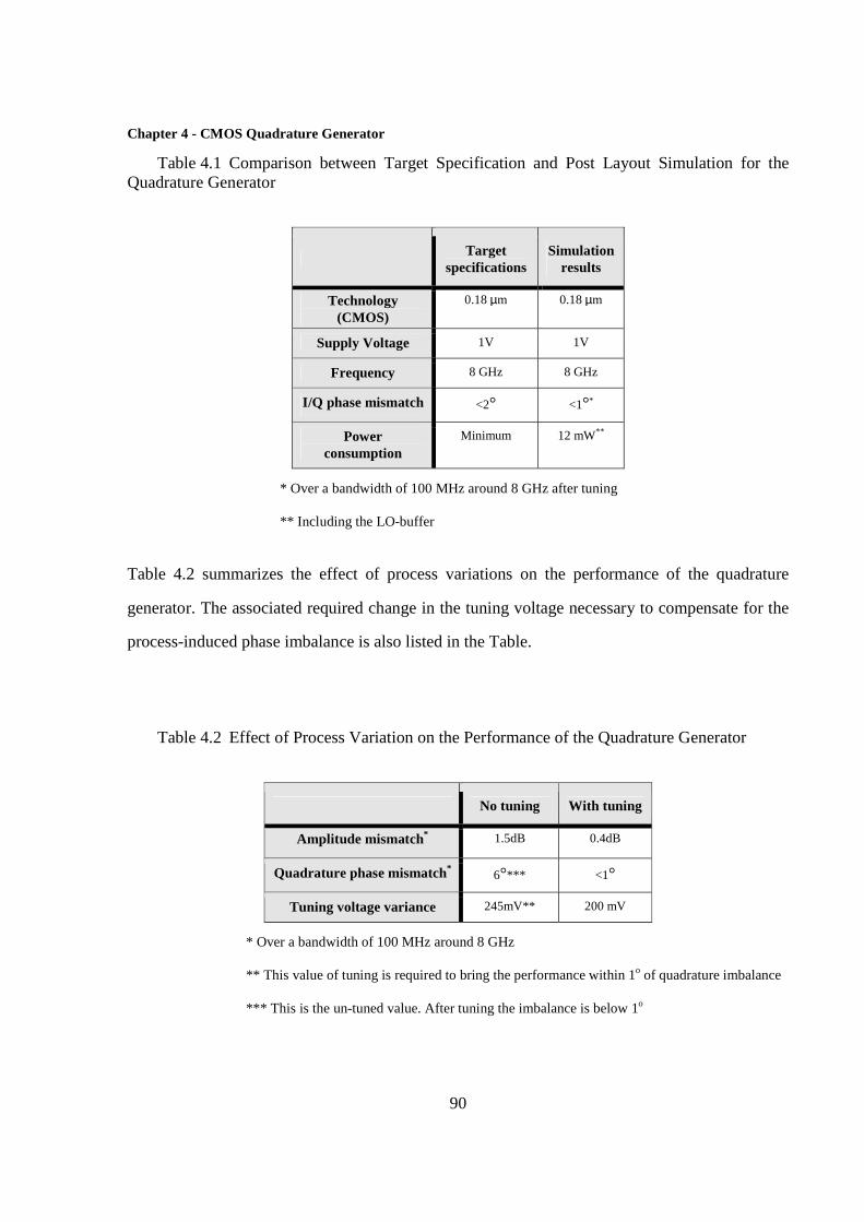
Chapter 4 - CMOS Quadrature Generator
90
Table 4.1 Comparison between Target Specification and Post Layout Simulation for the Quadrature Generator
Target
specifications Simulation
results
Technology (CMOS)
0.18 µm 0.18 µm
Supply Voltage 1V 1V
Frequency 8 GHz 8 GHz
I/Q phase mismatch <2° <1°*
Power consumption
Minimum 12 mW**
* Over a bandwidth of 100 MHz around 8 GHz after tuning
** Including the LO-buffer
Table 4.2 summarizes the effect of process variations on the performance of the quadrature
generator. The associated required change in the tuning voltage necessary to compensate for the
process-induced phase imbalance is also listed in the Table.
Table 4.2 Effect of Process Variation on the Performance of the Quadrature Generator
No tuning With tuning
Amplitude mismatch* 1.5dB 0.4dB
Quadrature phase mismatch* 6°*** <1 °
Tuning voltage variance 245mV** 200 mV
* Over a bandwidth of 100 MHz around 8 GHz
** This value of tuning is required to bring the performance within 1o of quadrature imbalance
*** This is the un-tuned value. After tuning the imbalance is below 1o

Chapter 4 - CMOS Quadrature Generator
91
The performance of the proposed quadrature generator was also simulated, using standard
technology parameters, over a temperature range of -25°C to 125°C. Table 4.3 summarizes the
simulation results for three operating temperatures of -25°C, 27°C and 125°C. The control
voltages are set for proper operation of the quadrature generator at 27°C. As mentioned
previously, the easy tunability of the circuit allows compensating for phase and amplitude
mismatches. The circuit specifications at other temperatures can be brought within the values
reported at 27°C, by applying a control voltage of less than 225 mV. Such a voltage can be
generated by previously reported automatic tuning circuitry [6].
Table 4.3 Effect of Temperature Variation on the Performance of the Quadrature Generator
-25°C 27°C 125°C
Amplitude mismatch* 0.5dB* 0.4dB* 0.6dB
Quadrature phase mismatch* < 1.6°* < 1°* < 3°*
Power consumption (mW) 11 ** 12 ** 13.6 **
* Over a bandwidth of 100 MHz around 8 GHz
** Including the LO-buffer
4.7 Summary
A novel quadrature generator architecture using active inductors was presented in this Chapter.
The design eliminates the need for buffers between the quadrature generator and the mixers and
thereby decreases the power consumption of the circuit. It relaxes the coupling between
quadrature phase and amplitude tuning which facilitates the phase and amplitude tuning of the
design to compensate for process and supply voltage variations. The post layout simulation
results confirm the tunability of the design and show that the quadrature generator satisfies the
quadrature accuracy and low voltage operation requirements of future generation of mobile
phones.

Chapter 4 - CMOS Quadrature Generator
92
References
[1] M. Steyaert and R. Roovers, “A 1-GHz Single-Chip Quadrature Modulator,” IEEE Journal of Solid-State Circuits, Vol. 27, pp. 1194 - 1197, 1992.
[2] F. Svelto, G. Montagna, S. Deantoni, G. Braschi and R. Castello, “Solutions for Image Re-jection CMOS LNA,” IEEE INternational Symposium on Circuits and Systems, pp. III-49 - III-52, 2000.
[3] F. Mahmoudi and C. Andre T. Salama, “8 GHz Tunable CMOS Quadrature Generator using Differential Active Inductors,” IEEE International Symposium on Circuits and Systems, pp. 2112 - 2115, 2005.
[4] R. Akbari-Dilmaghani, A. Payne and C. Toumazou, “A High Q RF CMOS Differential Ac-tive Inductor.” Proceedings of ICECS, pp. 157 - 160, 1998.
[5] J. Schechtman, A.C.M. De Queiroz and L.P. Caloba, “A High Performance Balanced MOS Transconductor,” IEEE 36th Midwest Symposium on Circuits and Systems, Proceedings pp.1378-1381, 1993.
[6] S. H. Wang, J. Gil, I. Kwon and H. K. Ahn, “A 5-GHz Band I/Q Clock Generator using a Self-Calibration Technique,” European Solid-State Circuits Conference, pp. 807 - 810, 2002.
[7] Virtuoso Spectre Circuit Simulator; http://www.cadence.com/products/custom_ic/spectre.
[8] M. Lefevre and P. Okrah, “Making the Leap to 4G Wireless,” EE Times, Network, Commu-nication System Design, pp. 26-32, July 2001.
[9] Y. Mochida, T. Takano, H. Gambe, “Future Directions and Technology Requirements of Wireless Communications,” IEEE International Electron Devices Meeting , Digest, pp. 1.3.1 - 1.3.8, 2001.

Chapter 5 - Implementations and Experimental Results
93
CHAPTER 5
CHAPTER 5: Implementations and Experimental Results
5.1 Introduction
This Chapter deals with the experimental implementation and characterization of the mixer, the
quadrature generator and the quadrature down-converter discussed in Chapters 2, 3 and 4. The
circuits are implemented using a standard CMOS 0.18 µm technology1.
5.2 Mixer Implementation and Characterization
Fig. 5.1 illustrates the micrograph of the implemented mixer using 0.18 µm CMOS technology.
The layout of the mixer was discussed in Chapter 3, section 3.6. The core area of the mixer is
320 x 400 µm2. The area of the complete test chip including the testing pads is 710 x 1080 µm2
[82,83].
1MOSTs are sensitive to electrostatic discharge (ESD). To avoid gate oxide breakdown, ESD protection
circuitry must be used at the input pads of the circuit. In the design kit under consideration, the behaviour of ESD protection circuits is not modeled at radio frequencies, and protection circuits were not used to allow for more accurate characterization of the building blocks under consideration.

Chapter 5 - Implementations and Experimental Results
94
Fig. 5.1 Micrograph of the fabricated mixer.
All measurements were carried out using on-chip probing. All probes were from GGB Industries
and featured a Signal-Ground-Signal (SGS) configuration. Measurements were conducted on
five different die samples to verify the repeatability of the results. All reported values are the
average of the five measured results1.
The setup used to measure the conversion gain and 1-dB compression point characteristics of the
mixer is illustrated in Fig. 5.2. It consists of: two signal generators (HP83712B and HP83650B)
used with two Narda 4346 180° hybrid to provide differential signals from the single ended
signal generator, four manual microwave tuners from Focus Microwaves (MMT 1808) used to
externally match the RF and LO ports of the mixer to 50Ω for correct measurements, four
Picosecond 5575A Bias-Tees to apply biasing to the mixer through HP E3631A DC power
supplies, a Mini-Circuit ZSCJ-2-1,2 180° 2-way combiner, used at the output of the mixer to
convert the differential output of the mixer to single ended and apply it to a HP8563E spectrum
analyzer. The output of the mixer was internally matched to 50Ω.
1 All available dies were from the same split with similar performances. The measurement variation associated with each performance metric for all five die samples are reported in the corresponding section.

Chapter 5 - Implementations and Experimental Results
95
Fig. 5.2 Mixer conversion gain and 1-dB compression point measurement setup.
Fig.5.3 illustrates a plot of the experimental and simulated power transfer characteristics of the
mixer. The experimental results reveal a 1-dB compression point of -5.5 dBm and a power
conversion gain (PCG) of +6.5 dB while operating from a supply voltage of 1V. By comparison,
the simulated power conversion gain and the 1-dB compression point are +10 dB and -8 dBm
respectively. The discrepancy between experimental and simulated results is partly due to
inaccuracies in the inductor and on-chip Metal-Insulator-Metal (MIM) capacitor, and partly due
to the parasitic resistances at the RF signal path which are not extracted by the design kit used.
The former effect is captured in simulation by correcting the resonance value based on
measurement results; and the latter is simulated by annotating parasitic resistances to the mixer
circuit. The residual discrepancy between measurement and simulation can be attributed to
device modeling inaccuracies at the operating frequency.
Five loose dies were measured. Gain and compression point variation among five dies were
0.15dB and 0.17dB respectively.

Chapter 5 - Implementations and Experimental Results
96
Fig. 5.3 Experimental and simulated conversion gain of the mixer.
The two-tone test setup shown in Fig. 5.4 was used to measure the IIP3 and IIP2 of the mixer.
The two RF tones located at 8001 MHz and 8003 MHz applied to the RF port of the mixer were
combined using a Mini-Circuits ZB4PD1-8.4, 4-way RF combiner (see Fig. 5.2 for the mixer test
core). The two unused inputs of the combiner were terminated to 50Ω broadband loads as shown
in the figure.
Fig. 5.4 Mixer two-tone test measurement setup.

Chapter 5 - Implementations and Experimental Results
97
Fig. 5.5 illustrates the two-tone experimental results. The intercept of the linear extrapolation of
the first and third order terms indicates an IIP3 of +3.5 dBm. The IIP2 of the mixer was found to
be better than +48 dBm. Due to the relatively high noise floor of the measurement setup,
particularly the spectrum analyzer, and the fact that the magnitude of the second order
nonlinearity was small and comparable to the noise floor for most values of the input signal
power below the 1-dB compression point of the mixer, it was only possible to conclude that the
IIP2 of the mixer is better than +48 dBm. The corresponding simulated results for IIP3 and IIP2
were +3 dBm and +52 dBm respectively. The higher experimental linearity observed is to be
expected due to the lower experimental gain discussed with reference to Fig. 5.2. Decreasing the
gain in a CCM, typically results in higher linearity. The measured IIP3 variation among all five
samples was 0.1dB.
Fig. 5.5 Two tone test plot of the mixer.

Chapter 5 - Implementations and Experimental Results
98
The test setup for characterizing the noise figure (NF) of the mixer is shown in Fig. 5.6. Manual
microwave tuners (MMT 1808) from Focus Microwaves were used to externally match the RF
port of the mixer to 50 Ω as required by definition, for correct measurements (see Fig. 5.2 for the
mixer test core). An HP8970B noise figure meter along with a NC346B noise source were used
to characterize the amount of noise degradation caused by the mixer under test. In the calibration
phase, the DUT was replaced by a thru connection, available on the calibration substrate of the
probes, to eliminate the parasitic effects of the measurement setup including the insertion loss
and the noise of the components.
Fig. 5.6 Mixer noise figure measurement setup.
The noise figure of the mixer was measured in the baseband frequency range of 10MHz to
200MHz1. The minimum noise figure at base band was 11.5dB. The noise figure variation
among all five samples is 0.35dB.
The isolation between the LO-port and the RF-port (LO to RF isolation) of the mixer at 8 GHz
was measured using the frequency domain method (S-parameter). The test setup is illustrated in
Fig. 5.7. For proper measurements, a full 2-port SOLT2 calibration was performed to bring the
reference plane of the S-parameter measurements to the tip of the RF probes, and eliminate the
1The lower end frequency of measurable NF was 10 MHz on the HP8970B noise figure meter. 2SOLT stands for Short-Open-Load-Thru.

Chapter 5 - Implementations and Experimental Results
99
parasitic effect of all the components between the network analyzer and the DUT (see Fig. 5.2
for the mixer test core).
The mixer exhibits an RF to LO isolation of better than 60 dB1 at 8 GHz. This result was
achieved by maximizing the separation of the RF and the LO sections of the mixer to minimize
the substrate assisted coupling between the two ports and by placing the transistors of the mixing
stage individually in deep N-wells isolated from the substrate.
Fig. 5.7 Mixer RF port to LO port isolation measurement setup.
The mixer design proposed in this work was completed and published in 2004. Tables 5.1 and
5.2 compare the present design to other low voltage mixers reported in the CMOS technology up
to 2005 and to date, respectively. As observed from the Tables, the architecture implemented in
this work relaxes the trade-off between power conversion gain and linearity which governs all
conventional CMOS active mixers while operating at low supply voltages. The power-
gain/linearity characteristics of the proposed design are superior to that of other low voltage
designs reported in the literature. This is a valuable feature, particularly in low voltage DCR
implementations.
1 Isolation measurement conducted on all five loose dies reveal RF to LO isolation better than 60dB.
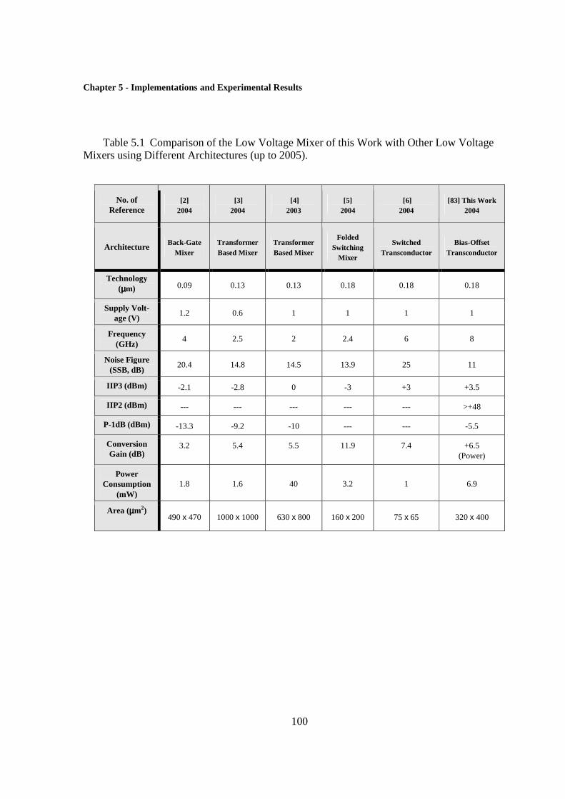
Chapter 5 - Implementations and Experimental Results
100
Table 5.1 Comparison of the Low Voltage Mixer of this Work with Other Low Voltage Mixers using Different Architectures (up to 2005).
No. of Reference
[2] 2004
[3] 2004
[4] 2003
[5] 2004
[6] 2004
[83] This Work 2004
Architecture Back-Gate
Mixer Transformer Based Mixer
Transformer Based Mixer
Folded Switching
Mixer
Switched Transconductor
Bias-Offset Transconductor
Technology (µµµµm) 0.09 0.13 0.13 0.18 0.18 0.18
Supply Volt-age (V)
1.2 0.6 1 1 1 1
Frequency (GHz)
4 2.5 2 2.4 6 8
Noise Figure (SSB, dB)
20.4 14.8 14.5 13.9 25 11
IIP3 (dBm) -2.1 -2.8 0 -3 +3 +3.5
IIP2 (dBm) --- --- --- --- --- >+48
P-1dB (dBm) -13.3 -9.2 -10 --- --- -5.5
Conversion Gain (dB)
3.2
5.4
5.5
11.9
7.4
+6.5 (Power)
Power Consumption
(mW) 1.8 1.6 40 3.2 1 6.9
Area (µµµµm2) 490 x 470 1000 x 1000 630 x 800 160 x 200 75 x 65 320 x 400

Chapter 5 - Implementations and Experimental Results
101
Table 5.2 Comparison of the Low Voltage Mixer of this Work with Other Low Voltage Mixers using Different Architectures (2005 to 2011)
No. of Reference
[29] 2007
[42] 2008
[36] 2008
[38] 2008
[58] 2011
[83] This Work
Architecture Back-Gate Mixer
Back-Gate Mixer
Transformer Based Mixer
Capacitor Coupled
Mixer
Cascode Bulk
Injection
Bias-Offset Transconductor
Technology (µµµµm) 0.18 0.18 0.18 0.18 0.18 0.18
Supply Volt-age (V)
0.8 1 0.8 1 0.7 1
Frequency (GHz)
2.4 5.8 5.8 2 6 8
Noise Figure (SSB, dB)
15 37 14.8 18 15.2 11
IIP3 (dBm) -5.7 15.3 3 11 0 +3.5
IIP2 (dBm) --- --- 19 --- --- >+48
P-1dB (dBm) --- 6.5 -3 2.2 --- -5.5
Conversion Gain (dB)
5.7
-0.8 -1.6
8.1
6
+6.5 (Power)
Power Consumption
(mW) 0.77 1 10 4.1 0.28 6.9
Area (µµµµm2) 180 x 200 300 x 500 1780 x 1390 900 x 900
150 x 236
320 x 400
Table 5.3 shows the linearity improvement achieved in this work compared to the conventional
CCM implemented in a standard 0.18 µm CMOS technology [7,52]. The first column in the
Table lists the characteristics of a conventional CCM (Fig.3.1(b)) optimized for linearity. The
second column shows the performance of a CCM with inductive degeneration (Fig. 3.4). The

Chapter 5 - Implementations and Experimental Results
102
third column shows the CCM mixer optimized for linearity using resistive degeneration. The
proposed design characteristics are listed in the third column. Note that the present mixer uses a
power supply of 1 V, while the conventional CCMs use a power supply of 1.8V. The
effectiveness of the proposed technique is evident since it achieves better linearity at lower
supply voltages compared to [7], The design using resistive degeneration achieves good linearity
at the expense of conversion gain and noise.
Table 5.3 Comparing the Linearity Characteristics of the Proposed Mixer and the Conventional CCM [7,52]
[7]-without
inductive source degeneration
[7]-with 15nH of inductive source
degeneration
[52] CCM with resistive source degeneration
[83] This work
0.18µµµµm
This work 65nm*
Technology (µµµµm) 0.18 0.18 0.18 0.18 0.065
Supply Voltage (V) 1.8V 1.8 1.8 1 0.9
Frequency (GHz) 2.45 2.45 5.8 8 8
Noise Figure (dB) 8.2 12.5 22 11.5 13
IIP3 (dBm) -12 -3.7 --- +3.5 3.2
IIP2 (dBm) --- --- --- >+48 ---
P-1dB (dBm) -21 -15.9 -2 -5.5 -5.7
Power Conversion Gain (dB)
+12 +2 -1 +6.5 5
Power Consumption (mW)
--- --- --- 6.9 6.2
* Simulation Results
Fig.5.8 summarizes the CMOS mixers published in the literature in various CMOS technologies.
The data points are arranged in terms of input-referred third order intercept point versus
10LOG(F-1), where F represents the noise factor of the circuit. The expression 10LOG(F-1)
indicates the amount in Decibels by which the input referred noise of the mixer sits above the

Chapter 5 - Implementations and Experimental Results
103
thermal noise floor. Fig.5.8 does not include the power consumption associated with the circuit.
It provides a clear view of the noise/linearity performance. The mixer design proposed in this
work is represented by the cross-shaped marker. The closer the marker is to the top left corner of
the plot, the better the noise/linearity performance of the mixer is. By scaling the linearity of the
circuit (IIP3) with its power consumption, in Fig.5.9, it is observed that the proposed design
stands at a fairly competitive spot in the plot, which highlights the low-power characteristics of
the proposed design. The plots in Figs 5.8 and 5.9 show that the proposed low-voltage, low
power linearity improvement technique is an effective technique [14-59]. The dashed line in
Fig.5.9 highlights the noise linearity tradeoff governing RF circuitry. Designs situated on the
dashed line trade linearity for noise or vice versa while samples closer to the top left corner of
the diagram, incorporate novelty to relax noise-linearity trade-off. The vertical cross represents
this work in 65nm CMOS. It is worth noting that by migrating to more advanced CMOS
technologies (i.e. 45nm or 28nm,…) the performance of the proposed mixer is expected to be
limited to the leftmost dashed line in Figure 5.9; Depending on noise/linearity tradeoff decision,
the mixer’s performance is expected to move along that line.
Fig. 5.8 CMOS mixers published in the literature [14-59]. Input referred third order intercept point versus noise.

Chapter 5 - Implementations and Experimental Results
104
Fig. 5.9 Proposed CMOS mixer compared to state of the art published work [14-59]. The vertical axis represents linearity over power in decibels.
5.3 Quadrature Generator Implementation and
Characterization
Fig. 5.10 shows the micrograph of the quadrature generator [84]. The core dimensions of the
design are 150 x 90 µm2. The dimensions of the complete test chip, including the testing pads are
1100 x 700 µm2. The layout of the quadrature generator was discussed in Chapter 4, section 4.5.
Measurements were carried on five separate dies to examine both the repeatability of the results
and the variances in quadrature phase and amplitude of the outputs under similar biasing and
control voltage conditions. All reported values are the average of the values obtained from five
measured chips.

Chapter 5 - Implementations and Experimental Results
105
90 µm
150
µ m
Fig. 5.10 Micrograph of the fabricated quadrature generator in 0.18µm CMOS.
The setup used to measure the quadrature phase and amplitude accuracy at the output of the
quadrature generator is illustrated in Fig. 5.11. A Tektronix TDS8000 oscilloscope was used to
characterize the output waveform of the quadrature generator in the time domain.
Fig. 5.11 Quadrature Generator measurement setup.
Fig. 5.12 is a plot of the measured quadrature phase and amplitude matching of the design. Post
layout simulation results are also shown for the purpose of comparison. The slight discrepancy

Chapter 5 - Implementations and Experimental Results
106
between the measured and simulated results is mainly attributed to the uncertainty in
measurements due to the built-in jitter of the equipment and the phase and amplitude error
introduced by the interconnections. The circuit demonstrates a quadrature phase and amplitude
matching of better than 1.5° and 1 dB over the bandwidth of interest. The fine tuning of the
quadrature generator performance for all the measured samples requires applying a variation of
less than 150 mV in VC (4° of variance in the output quadrature phase) and less than 80 mV in
VB1 (1 dB of variance in amplitude) to achieve the experimental values reported in Fig. 5.12.
These control voltage variations can be generated by automatic amplitude and phase tuning
circuitry previously reported in the literature [8]. Given the tenability of the design, all five
measured dies were tuned to the same performance levels with less than 10mV and 5mV
variance in VC and VB1 respectively.
(a)
(b)
Fig. 5.12 Measured and simulated results for quadrature phase and amplitude accuracy of the quadrature generator. (a) Quadrature phase accuracy. (b) Quadrature amplitude.

Chapter 5 - Implementations and Experimental Results
107
Fig. 5.13 illustrates the measured time domain representation of the outputs of the quadrature
generator without applying averaging on the results. The gain of the fabricated quadrature
generator at 8 GHz is almost 2 dB lower than the simulated value. This discrepancy is due to the
parasitic resistances which are not extracted by the design kit used in this work.
Fig. 5.13 Time domain output of the quadrature generator measured at 8GHz.
The phase noise was measured with and without the device under test using the test setup
illustrated in Fig. 5.14, and the result is illustrated in Fig. 5.15. The signal generator phase noise
is low. The measurement setup includes an HP8560A spectrum analyzer equipped with a 85671
phase noise utility from Agilent Technologies. The plots in Fig. 5.15, reveals that the phase noise
at the output of the quadrature generator is -108 dBc/Hz at 1 MHz offset frequency.
Fig. 5.14 Quadrature generator phase-noise measurement setup.

Chapter 5 - Implementations and Experimental Results
108
Fig. 5.15 Measured phase noise of the quadrature generator.
The experimental performance of the proposed design is compared to four previous designs
reported prior to 2005 [8-11] and more recent designs in Table 5.4 and Table 5.5 respectively.
Each design uses a different architecture to generate quadrature signals, as listed in the Table. By
comparison, the design proposed in this work, reduces the power consumption by omitting the
buffers between the quadrature generator and the mixers. It also relaxes the coupling between
amplitude and phase tuning which facilitates the use of automatic amplitude and phase tuning
circuitry. The design also features a very small form factor since it does not include passive
devices.
Fig.5.16 summarizes previously published quadrature generator work [60-81]. The vertical axis
shows the phase noise at 1MHz offset and the horizontal axis represents the quadrature phase
error. The closer the design is to the lower left corner, the better the design is. The quadrature
generator designed in this work is represented by the cross shaped marker.

Chapter 5 - Implementations and Experimental Results
109
The two rectangle shaped points are quadrature VCOs based on bulk acoustic wave (BAW)
technology. This circuit is capable of achieving excellent phase noise performance at the expense
of increased cost due to the placement of the BAW resonator inside the package. The diamond
point at the top left corner represents an LC quadrature oscillator equipped with phase tuning
capability. The added phase tuning circuitry considerably degraded the phase noise performance
of the design.
Table 5.4 Comparison of the Proposed Quadrature Generator to Previous Work up to 2004.
No. of Reference [8]
2002 [9]
2002 [10] 2003
[11] 2004
[84] This Work 2005
Architecture One Stage Ploy-Phase
Filter
Quadrature LC
Oscillator
Ring Oscillator
Four Stage Poly-Phase
Filter
Active Inductors
Technology CMOS 0.18µm
CMOS 0.18µm
CMOS 0.18µm
BICMOS 0.4µm
CMOS 0.18µm
Supply Voltage 1.8 V 1.8 V 1.8 V 2.5 V 1 V
Frequency 5 GHz 2.5 GHz 3.5 GHz 5.8 GHz 8 GHz
Phase Mismatch 2° <1.2° < 3.2° 5° 1.5°
Amplitude Mismatch --- <5% --- --- <1 dB
Area 0.12 mm2 0.55 mm2 --- 0.183 mm2 0.009 mm2
Power Consumption 2.7 mW* 7.2 mW* 16.2 mW* 50 mW 12 mW**
* This number does not include the power consumption of the buffers used in the design
** Including the LO buffer

Chapter 5 - Implementations and Experimental Results
110
Table 5.5 Comparison of the Proposed Quadrature Generator to Previous Work up to 2011.
No. of Reference [80] 2010
[73] 2008
[67] 2009
This Work 2011
[84] This Work 2005
Architecture QVCO Divider Poly-Phase Filter
Active Inductors
Active Inductors
Technology CMOS 65 nm CMOS 0.18µm
CMOS 0.18µm
CMOS 65 nm CMOS 0.18µm
Supply Voltage 1.0 V 1.8 V 1.8 V 1.0 V 1 V
Frequency 4.5 GHz 1.57 GHz 10 GHz 15 GHz* 8 GHz
Phase Mismatch 2° 6° < 0.15° 2.1°* 1.5°
Amplitude Mismatch --- 12% 0.2dB 0.8dB* <1 dB
Area 0.28 mm2 --- --- --- 0.009 mm2
Power Consumption 43 mW 3.06 mW --- 9 mW 12 mW
* Based on simulation
Fig. 5.16 Quadrature generator comparison to previous work [60-81].

Chapter 5 - Implementations and Experimental Results
111
5.4 Quadrature Down-converter Implementation and
Characterization
Fig. 5.17 shows the micrograph of the complete quadrature down-converter including two mixers
and a quadrature down-converter tested in sections 5.2 and 5.3 respectively. The dimensions of
the chip including the testing pads are 1000 x 1360 µm2 [85].
Fig. 5.17 Micrograph of the fabricated quadrature down-converter.
The quadrature down-converter circuit of Fig. 5.17 was used to measure the image rejection ratio
(IRR) of the circuit. The approach suggested in reference [12] was used in this measurement and
the test setup is illustrated in Fig. 5.18. Two -25dBm RF signals, equally spaced around the 8
GHz LO signal were applied at the RF inputs. The two RF signals were varied from 7.95 GHz
and 8.05 GHz to 7.999 GHz and 8.001 GHz to cover the bandwidth of interest of 100 MHz.
The measured IRR over a bandwidth of 100 MHz is illustrated in Fig. 5.19. The quadrature
phase and amplitude accuracy of the quadrature generator can be inferred from the measured
IRR by referring to the plots in reference [13], as mentioned in Chapter 2. It is observed that the

Chapter 5 - Implementations and Experimental Results
112
measured IRR shown in Fig. 5.19 corresponds to a quadrature phase mismatch of better than 2°
over the RF bandwidth of interest.
Fig. 5.18 Image-rejection ratio measurement setup.
Fig. 5.19 Image rejection ration measurement results over 100MHz IF bandwidth.

Chapter 5 - Implementations and Experimental Results
113
Table 5.6 summarizes the quadrature phase and amplitude accuracy obtained from both time
domain measurements on the quadrature generator alone and IRR measurements on the
quadrature down-converter. The results from time domain measurements are listed for an LO
frequency of 8 GHz. The amplitude and quadrature phase error extracted from the IRR method
are obtained for fixed LO frequency at 8 GHz and varying the RF signal over a bandwidth of 100
MHz around the carrier frequency of 8 GHz. The Proposed QD is compared to DCRs targeting
similar applications in table 5.7.
Table 5.6 I/Q Amplitude and Quadrature Phase Error Obtained from the IRR Method and the Time Domain Characterization
Amplitude
Error Quadrature Phase Error]
IRR Method --- < 2°
Time Domain Method 1.5dB** 1.5°
Table 5.7 Quadrature Down-converter (QD) compared to other DCRs targeting similar applications.
Architecture DCR [86]
2010 DCR [87]
2010 This Work [85]
2006
Technology 0.13µm CMOS 0.18µm CMOS 0.18µm CMOS
Supply Voltage 1.2V 1.8V 1.0V
Frequency 5.8GHz 6GHz 8GHz
IRR 37dB 40dB 40dB
Gain +48dB* --- +6dB
Area 6.24mm2* 2.1mm2* 1.36mm2
Power 52mW* 75mW* 25.8mW
* Based on simulation
**The power, area and gain numbers include LNA and baseband filters

Chapter 5 - Implementations and Experimental Results
114
5.5 Summary
The implementation and characterization of an 8 GHz CMOS mixer with improved linearity
under low supply voltage, and a quadrature generator with easy tunability suited for direct
conversion receivers were discussed in this Chapter. They are implemented in TSMC’s CMOS
0.18µm technology. The experimental results were in reasonable agreement with the simulated
data and the analytical expressions describing the behaviour of both circuits in Chapters 3 and 4.
The mixer architecture relaxes the inherent trade-off between power conversion gain and
linearity. The quadrature generator circuit relaxes the coupling between the amplitude and
quadrature phase tuning which makes it easier to apply automatic tuning circuitry to the design
to compensate for temperature and process variations. It also decreases the power consumption
by omitting the buffers located between the quadrature generator and the mixers. The mixer and
the quadrature generator meet the potential target specifications of the future generation of
mobile phones in terms of low supply voltage and good linearity requirements.

Chapter 5 - Implementations and Experimental Results
115
References
[1] T. W. Kim, B. Kim and K. Lee, “Highly Linear RF CMOS Amplifier and Mixer Adopting MOSFET Transconductance Linearization by Multiple Gated Transistors,” IEEE Radio Frequency Integrated Circuits Symposium, Proceedings, pp. 107-110, 2003.
[2] C. Kienmayer, M. Tiebout, W. Simburger and A. L. Scholtz, “A Low-Power Low-Voltage NMOS Bulk-Mixer With 20 GHz Bandwidth in 90 nm CMOS,” International Symposium on Circuits and Systems, Vol. 4, pp. 385 - 388, 2004.
[3] C. Hermann, M. Tiebout and H. Klar, “A 0.6V 1.6 mW Transformer Based 2.5 GHz Downconversion Mixer with +5.4dB Gain and -2.8 dBm IIP3 in 0.13m CMOS,” IEEE Radio Frequency Integrated Circuit Symposium, pp. 35 - 38, 2004.
[4] M. Tiebout and T. Leibermann, “A 1V Fully Integrated CMOS Transformer Based Mixer With 5.5dB gain, 14.5 dB SSB Noise Figure and 0 dBm Input IP3,” European Solid-State Circuits Conference, pp. 577 - 580, 2003.
[5] V. Vidojkovic, J. Van Der Tang, A. Leeuwenburgh and A. Van Roermund, “A High Gain, Low Voltage Folded-Switching Mixer With Current-Reuse In 0.18m CMOS,” IEEE Radio Frequency Integrated Circuit Symposium, pp. 31 - 34, 2004.
[6] E. A. M. Klumperink, S. M. Louwsma, G. J. M. Wienk and B. Nauta, “A CMOS Switched Transconductor Mixer,” IEEE Journal of Solid-State Circuits, Vol. 39, pp. 1231 - 1240, 2004.
[7] Q. Li, J. Zhang, W. Li and J. S. Yuan, “CMOS RF Mixer Non-Linearity Design,” IEEE 43rd Midwest symposium on Circuits and Systems, Proceedings, pp. 808 - 811, 2001.
[8] S. H. Wang, J. Gil, I. Kwon and H. K. Ahn, “A 5-GHz Band I/Q Clock Generator using a Self-Calibration Technique,” European Solid-State Circuits Conference, pp. 807 - 810, 2002.
[9] D. Leenaerts, C. Dijkmans and M. Thompson, “A 0.18m CMOS 2.45 GHz Low-Power Quadrature VCO with 15% Tuning Range,” IEEE Radio Frequency Integrated Circuit Symposium, pp. 67 - 69, 2002.
[10] M. Grozing, B. Phillip and M. Berroth, “CMOS Ring Oscillator with Quadrature Outputs and 100 MHz to 3.5 GHz Tuning Range,” European Solid-State Circuits Conference, pp. 679 - 682, 2003.
[11] D. I. Sanderson, R. M. Svitek and S. Raman, “A 5-6-GHz Polyphase Filter with Tunable I/Q Phase Balance,” IEEE Microwave and Wireless Component Letters, Vol. 14, pp. 364 - 366, July 2004.
[12] C.-H. Wu, C.-C. Tang, K.-H. Li and S.-I. Liu, “CMOS 2.4 GHz Receiver Front End with

Chapter 5 - Implementations and Experimental Results
116
Area-Efficient Inductors and Digitally Calibrated 90 Delay Network,” IEE Circuit, Devices and Systems Proceedings, Vol. 150, pp. 439 - 444, 2003.
[13] J. P. Maligeorgos and John R. Long, “A Low-Voltage 5.1-5.8 GHz Image Reject Receiver with Wide Dynamic Range,” IEEE Journal of Solid-State Circuits, Vol. 35, pp. 1917 - 1926, 2000.
[14] Belkhiri, C.; Toutain, S.; Razban, T.; , "Wide bandwidth and low power CMOS mixer with
high linearity for multiband receivers using direct conversion implementation," Microwave Conference, 2005 European , vol.3, pp. 4 pp., 4-6 Oct. 2005
[15] Perumana, B.G.; Chang-Ho Lee; Laskar, J.; Chakraborty, S.; , "A subharmonic CMOS mix-er based on threshold voltage modulation," Microwave Symposium Digest, 2005 IEEE MTT-S International , vol., pp. 4 pp., 12-17 June 2005
[16] Pekau, H.; Haslett, J.W.; , "A 2.4 GHz CMOS sub-sampling mixer with integrated filter-ing," Solid-State Circuits, IEEE Journal of , vol.40, no.11, pp. 2159- 2166, Nov. 2005
[17] Pekau, H.; Haslett, J.W.; , "A 2.4 GHz CMOS sub-sampling mixer with integrated filter-ing," Solid-State Circuits, IEEE Journal of , vol.40, no.11, pp. 2159- 2166, Nov. 2005
[18] Vidojkovic, V.; van der Tang, J.; Leeuwenburgh, A.; van Roermund, A.H.M.; , "A low-voltage folded-switching mixer in 0.18-µm CMOS," Solid-State Circuits, IEEE Journal of , vol.40, no.6, pp. 1259- 1264, June 2005
[19] Upadhyaya, P.; Rajashekharaiah, M.; Deukhyoun Heo; Chen, Y.-J.E.; , "A high IIP2 doubly balanced sub-harmonic mixer in 0.25-µm CMOS for 5-GHz ISM band direct conversion re-ceiver," Radio Frequency integrated Circuits (RFIC) Symposium, 2005. Digest of Papers. 2005 IEEE , pp. 175- 178, 12-14 June 2005
[20] Pavaluta, C.M.; Neacsu, C.M.; Dimitriu, B.; Ionascu, C.; , "Low noise CMOS mixers," Sig-nals, Circuits and Systems, 2005. ISSCS 2005. International Symposium on , vol.2, pp. 685- 688 Vol. 2, 14-15 July 2005
[21] No Gil Myoung; Byoung Gun Choi; Seong Su Park; Chul Soon Park; , "A novel CMOS down-conversion mixer with current reuse technique," Microwave Conference Proceedings, 2005. APMC 2005. Asia-Pacific Conference Proceedings , vol.5, pp. 4 pp., 4-7 Dec. 2005
[22] Dufrene, K.; Weigel, R.; , "Highly linear IQ downconverter for reconfigurable wireless re-ceivers," Wireless Technology, 2005. The European Conference on , pp.19-22, 3-4 Oct. 2005

Chapter 5 - Implementations and Experimental Results
117
[23] Wei-Chia Zhan; Chien-Nan Kuo; Jyh-Chyurn Guo; , "Low-power and high-linearity mixer design using complex transconductance equivalent circuit," Custom Integrated Circuits Conference, 2005. Proceedings of the IEEE 2005 , pp.365-368, 21-21 Sept. 2005
[24] Brandolini, M.; Rossi, P.; Sanzogni, D.; Svelto, F.; , "A +78 dBm IIP2 CMOS direct downconversion mixer for fully integrated UMTS receivers," Solid-State Circuits, IEEE Journal of , vol.41, no.3, pp. 552- 559, March 2006
[25] Lu Liu; ZhiHua Wang; , "Analysis and design of a low-voltage RF CMOS mixer," Circuits and Systems II: Express Briefs, IEEE Transactions on , vol.53, no.3, pp. 212- 216, March 2006
[26] Dufrene, K.; Weigel, R.; , "A novel IP2 calibration method for low-voltage downconversion mixers," Radio Frequency Integrated Circuits (RFIC) Symposium, 2006 IEEE , pp.4 pp.-292, 11-13 June 2006
[27] Shi, B.; Chia, M.Y.W.; , "A CMOS Receiver Front-End for 3.1-10.6 GHz Ultra-Wideband Radio," Radar Conference, 2006. EuRAD 2006. 3rd European , pp.350-353, 13-15 Sept. 2006
[28] Kihwa Choi; Dong Hun Shin; Yue, C.P.; , "A 1.2-V, 5.8-mW, Ultra-Wideband Folded Mix-er in 0.13-µm CMOS," Radio Frequency Integrated Circuits (RFIC) Symposium, 2007 IEEE , pp.489-492, 3-5 June 2007
[29] Kung-Hao Liang; Hong-Yeh Chang; Yi-Jen Chan; , "A 0.5–7.5 GHz Ultra Low-Voltage Low-Power Mixer Using Bulk-Injection Method by 0.18- µm CMOS Technology," Micro-wave and Wireless Components Letters, IEEE , vol.17, no.7, pp.531-533, July 2007
[30] Brandolini, M.; Sosio, M.; Svelto, F.; , "A 750 mV Fully Integrated Direct Conversion Re-ceiver Front-End for GSM in 90-nm CMOS," Solid-State Circuits, IEEE Journal of , vol.42, no.6, pp.1310-1317, June 2007
[31] Sheng-Che Tseng; Chinchun Meng; Guo-Wei Huang; , "High gain cmos gilbert downcon-verter with wide-swing cascode current-mirror transconductor and load," Antennas and Propagation Society International Symposium, 2007 IEEE , pp.4513-4516, 9-15 June 2007
[32] Bo Shi; Michael; Yan Wah Chia; , "A 3-10-GHz 0.13-µm CMOS receiver front-end for MB-OFDM ultra-wideband systems," Ultra-Wideband, 2007. ICUWB 2007. IEEE Interna-tional Conference on , pp.622-625, 24-26 Sept. 2007
[33] Theodoratos, G.; Papananos, Y.; Vitzilaios, G.; , "A Low-Voltage 5-GHz Downconversion Mixer Employing A Second Harmonic Injection Linearization Technique," Circuits and Sys-tems II: Express Briefs, IEEE Transactions on , vol.54, no.11, pp.964-968, Nov. 2007

Chapter 5 - Implementations and Experimental Results
118
[34] Zhang, R.-X.; Shi, C.-Q.; Lai, Z.-S.; , "Linearity enhancement technology for mixer in monolithic CMOS UHF RFID interrogator," Electronics Letters , vol.44, no.14, pp.855-856, July 3 2008
[35] Jehyung Yoon; Huijung Kim; Changjoon Park; Jinho Yang; Hyejeong Song; Sekyeong Lee; Bumman Kim; , "A New RF CMOS Gilbert Mixer With Improved Noise Figure and Linear-ity," Microwave Theory and Techniques, IEEE Transactions on , vol.56, no.3, pp.626-631, March 2008
[36] Lai, J.-T.; Lin, Y.-S.; Lu, C.-L.; Chuang, H.-R.; , "A 3-5-GHz Low-Voltage High-Isolation Transformer-Based CMOS Mixer for UWB Applications," Innovative Computing Infor-mation and Control, 2008. ICICIC '08. 3rd International Conference on , pp.238, 18-20 June 2008
[37] Vahidfar, M.B.; Shoaei, O.; Svelto, F.; , "A high dynamic range multi-standard CMOS mix-er for GSM, UMTS and IEEE802.11b-g-a applications," Radio Frequency Integrated Cir-cuits Symposium, 2008. RFIC 2008. IEEE , pp.193-196, June 17 2008-April 17 2008
[38] Senhg-Feng Lu; Jyh-Chyurn Guo; , "5.5 GHz Low Voltage and High Linearity RF CMOS Mixer Design," Microwave Integrated Circuit Conference, 2008. EuMIC 2008. European , pp.171-174, 27-28 Oct. 2008
[39] Krcmar, M.; Subramanian, V.; Jamal Deen, M.; Boeck, G., "High gain low noise folded CMOS mixer," Wireless Technology, 2008. EuWiT 2008. European Conference on , pp.13-16, 27-28 Oct. 2008
[40] Mumin Lei; Haiying Zhang; Changming Ma; , "A 6∼9 GHz Bi-quadrature folded-switching down-conversion mixer for MB-OFDM UWB application in 0.18 µm CMOS technology," Solid-State and Integrated-Circuit Technology, 2008. ICSICT 2008. 9th International Con-ference on , pp.1496-1499, 20-23 Oct. 2008
[41] Manstretta, D.; , "High Linearity Down-Conversion CMOS Mixers," Microwave Integrated Circuit Conference, 2008. EuMIC 2008. European , pp.175-178, 27-28 Oct. 2008
[42] Van Vorst, D.; Mirabbasi, S.; , "Low-power 1V 5.8 GHz bulk-driven mixer with on-chip balun in 0.18µm CMOS," Radio Frequency Integrated Circuits Symposium, 2008. RFIC 2008. IEEE , pp.197-200, June 17 2008-April 17 2008
[43] Schweiger, K.; Zimmermann, H.; , "A 24dB gain Gilbert-type down-sampling mixer with increased DC-input range through exploiting the body effect," Mixed Design of Integrated Circuits and Systems, 2008. MIXDES 2008. 15th International Conference on , pp.151-154, 19-21 June 2008

Chapter 5 - Implementations and Experimental Results
119
[44] Zhong-Cheng Su; Zhi-Ming Lin; , "A 18.9dB conversion gain folded mixer for WiMAX system," Circuits and Systems, 2008. APCCAS 2008. IEEE Asia Pacific Conference on , pp.292-295, Nov. 30 2008-Dec. 3 2008
[45] Kanaya, H.; Koga, N.; Abdelghany, M.A.; Pokharel, R.K.; Yoshida, K.; , "Low flicker-noise and low leakage direct conversion CMOS mixer for 5GHz application," Microwave Conference, 2009. APMC 2009. Asia Pacific , pp.1631-1634, 7-10 Dec. 2009
[46] Pei-Zong Rao; Tang-Yuan Chang; Ching-Piao Liang; Shyh-Jong Chung; , "An Ultra-Wideband High-Linearity CMOS Mixer With New Wideband Active Baluns," Microwave Theory and Techniques, IEEE Transactions on , vol.57, no.9, pp.2184-2192, Sept. 2009
[47] Deguchi, J.; Miyashita, D.; Hamada, M.; , "A 0.6V 380µW −14dBm LO-input 2.4GHz dou-ble-balanced current-reusing single-gate CMOS mixer with cyclic passive combiner," Solid-State Circuits Conference - Digest of Technical Papers, 2009. ISSCC 2009. IEEE Interna-tional , pp.224-225,225a, 8-12 Feb. 2009
[48] Xuan, K.; Tsang, K.F.; Lee, S.C.; Lee, W.C.; , "High-performance current bleeding CMOS mixer," Electronics Letters , vol.45, no.19, pp.979-981, September 10 2009
[49] Chang-Wan Kim; Hae-Won Son; Bong-Soon Kang; , "A 2.4 GHz Current-Reused CMOS Balun-Mixer," Microwave and Wireless Components Letters, IEEE , vol.19, no.7, pp.464-466, July 2009
[50] Hampel, S.K.; Schmitz, O.; Tiebout, M.; Rolfes, I.; , "Low-voltage, inductorless folded down-conversion mixer in 65nm CMOS for UWB applications," Radio Frequency Integrat-ed Circuits Symposium, 2009. RFIC 2009. IEEE , pp.119-122, 7-9 June 2009.
[51] Hyo-Rim Bae; Choon Sik Cho; Lee, J.W.; Jaeheung Kim; , "A 24GHz dual-gate mixer us-ing sub-harmonic in 0.18µm CMOS technology," Microwave Conference, 2009. APMC 2009. Asia Pacific , pp.1739-1742, 7-10 Dec. 2009
[52] Fan Xiangning; Zhang Lei; Zhu Chisheng; Wu Rui; , "Implementation of an improved ac-tive CMOS mixer with high linearity for wideband wireless systems," Signals Systems and Electronics (ISSSE), 2010 International Symposium on , vol.2, pp.1-4, 17-20 Sept. 2010
[53] Ro-Min Weng; Shu-Wei Liu; , "A 1.5V low noise figure mixer for 3.5GHz WiMAX sys-tems," Circuits and Systems (ISCAS), Proceedings of 2010 IEEE International Symposium on , pp.2211-2214, May 30 2010-June 2 2010
[54] Song Hu; Weinan Li; Yumei Huang; Zhiliang Hong; , "Design of a high linearity low noise mixer for low voltage application," Solid-State and Integrated Circuit Technology (ICSICT), 2010 10th IEEE International Conference on , pp.653-655, 1-4 Nov. 2010

Chapter 5 - Implementations and Experimental Results
120
[55] Gao Junjun; Cheng Zhiqun; Zhu Xuefang; Xu Shengjun; , "A high performance CMOS even harmonic mixer with a LC resonant circuit," Microwave and Millimeter Wave Tech-nology (ICMMT), 2010 International Conference on , pp.449-453, 8-11 May 2010
[56] Schweiger, K.; Zimmermann, H.; , "Highly linear down-conversion mixer in 65nm CMOS for a high supply voltage of 2.5V," Design and Diagnostics of Electronic Circuits and Sys-tems (DDECS), 2010 IEEE 13th International Symposium on , pp.205-208, 14-16 April 2010
[57] Feng Zhou; Wei Li; Ting Gao; Fei Lan; Ning Li; Junyan Ren; , "A single-in-differential-out CMOS RF front-end for UWB 6–9GHz applications," Solid-State and Integrated Circuit Technology (ICSICT), 2010 10th IEEE International Conference on , pp.743-745, 1-4 Nov. 2010
[58] Liang, K.-H.; Chang, H.-Y.; , "0.5-6 ghz low-voltage low-power mixer using a modified cascode topology in 0.18 µm cmos technology," Microwaves, Antennas & Propagation, IET , vol.5, no.2, pp.167-174, Jan. 31 2011.
[59] Ho, S.S.K.; Saavedra, C.E.; , "A CMOS Broadband Low-Noise Mixer With Noise Cancella-tion," Microwave Theory and Techniques, IEEE Transactions on , vol.58, no.5, pp.1126-1132, May 2010
[60] Rai, S.; Otis, B.; , "A 1V 600µW 2.1GHz Quadrature VCO Using BAW Resonators," Solid-State Circuits Conference, 2007. ISSCC 2007. Digest of Technical Papers. IEEE Interna-tional , pp.576-623, 11-15 Feb. 2007
[61] Kuang-Wei Cheng; Natarajan, K.; Allstot, D.J.; , "A Current Reuse Quadrature GPS Re-ceiver in 0.13 m CMOS," Solid-State Circuits, IEEE Journal of , vol.45, no.3, pp.510-523, March 2010
[62] Mazzanti, A.; Svelto, F.; , "A 1.8-GHz injection-locked quadrature CMOS VCO with low phase noise and high phase accuracy," Circuits and Systems I: Regular Papers, IEEE Trans-actions on , vol.53, no.3, pp.554-560, March 2006
[63] Chung-Yu Wu; Chung-Yun Chou; , "A 5-GHz CMOS double-quadrature receiver front-end with single-stage quadrature generator," Solid-State Circuits, IEEE Journal of , vol.39, no.3, pp. 519- 521, March 2004
[64] Guochi Huang; Byung-Sung Kim; , "Programmable Active Inductor Based Quadrature VCO Design," Microwave Conference, 2007. APMC 2007. Asia-Pacific , pp.1-4, 11-14 Dec. 2007

Chapter 5 - Implementations and Experimental Results
121
[65] Jackson, B.R.; Saavedra, C.E.; , "A 3 GHz CMOS Quadrature oscillator using active super-harmonic coupling," Microwave Integrated Circuit Conference, 2007. EuMIC 2007. Euro-pean , pp.311-314, 8-10 Oct. 2007
[66] Zafar, S.; Awan, M.; Zulkifli, T.Z.A.; , "5-GHz low-phase noise quadrature VCO in 0.13−µm RF CMOS process technology," Wireless and Microwave Technology Conference, 2009. WAMICON '09. IEEE 10th Annual , pp.1-4, 20-21 April 2009
[67] Syu, J.-S.; Meng, C.; Teng, Y.-H.; , "10 GHz dual-conversion low-IF downconverter with microwave and analogue quadrature generators," Electronics Letters , vol.45, no.13, pp.685 -686, June 18 2009
[68] Hsieh-Hung Hsieh; Ying-Chih Hsu; Liang-Hung Lu; , "A 15/30-GHz Dual-Band Multi-phase Voltage-Controlled Oscillator in 0.18- µm CMOS," Microwave Theory and Tech-niques, IEEE Transactions on , vol.55, no.3, pp.474-483, March 2007
[69] Sangjin Byun; Kwan-Woo Kim; Dong-Ho Lee; Laskar, J.; Cheon Soo Kim; , "A self-calibrated LC quadrature VCO in a current-limited region," Radio Frequency Integrated Circuits Symposium, 2008. RFIC 2008. IEEE , pp.379-382, June 17 2008-April 17 2008
[70] Jong-Phil Hong; Seok-Ju Yun; Nam-Jin Oh; Sang-Gug Lee; , "A 2.2-mW Backgate Cou-pled LC Quadrature VCO With Current Reused Structure," Microwave and Wireless Com-ponents Letters, IEEE , vol.17, no.4, pp.298-300, April 2007
[71] Sheng-Lyang Jang; Yun-Hsueh Chuang; Chien-Keng Lee; Shao-Hua Lee; , "A 4.8GHz Low-Phase Noise Quadrature Colpitts VCO," VLSI Design, Automation and Test, 2006 In-ternational Symposium on , pp.1-4, 26-28 April 2006
[72] Hara, S.; Okada, K.; Matsuzawa, A.; , "10MHz to 7GHz quadrature signal generation using a divide-by-4/3, -3/2, -5/3, -2, -5/2, -3, -4, and -5 injection-locked frequency divider," VLSI Circuits (VLSIC), 2010 IEEE Symposium on , pp.51-52, 16-18 June 2010
[73] Kyung-Gyu Park; Chan-Young Jeong; Jae-Woo Park; Jang-Woo Lee; Jun-Gi Jo; Changsik Yoo; , "Current Reusing VCO and Divide-by-Two Frequency Divider for Quadrature LO Generation," Microwave and Wireless Components Letters, IEEE , vol.18, no.6, pp.413-415, June 2008
[74] Saeedi, S.; Atarodi, M.; Bakhtiar, M.S.; , "A divide-by-3 frequency divider for I/Q genera-tion in a multi-band frequency synthesizer," Circuits and Systems, 2008. APCCAS 2008. IEEE Asia Pacific Conference on , pp.1383-1386, Nov. 30 2008-Dec. 3 2008
[75] Kuang-Wei Cheng; Allstot, D.J.; , "A gate-modulated CMOS LC quadrature VCO," Radio Frequency Integrated Circuits Symposium, 2009. RFIC 2009. IEEE , pp.267-270, 7-9 June 2009

Chapter 5 - Implementations and Experimental Results
122
[76] Roufoogaran, R.; Li, T.; Ojo, A.; Cheng, S.; Lee, C.P.; Mahadeva, S.; Shetter, P.; Behzad, A.; , "A compact and power efficient local oscillator generation and distribution system for complex multi radio systems," Radio Frequency Integrated Circuits Symposium, 2008. RFIC 2008. IEEE , pp.277-280, June 17 2008-April 17 2008
[77] Pandey, J.; Amrutur, B.; Kudva, S.; , "Quadrature generation techniques for frequency mul-tiplication based oscillators," Circuits and Systems, 2008. ISCAS 2008. IEEE International Symposium on , pp.440-443, 18-21 May 2008
[78] Chamas, I.R.; Raman, S.; , "A 5 GHz I/Q Phase-tunable CMOS LC Quadrature VCO (PT-QVCO) for Analog Phase Calibrated Receiver Architectures," Silicon Monolithic Integrated Circuits in RF Systems, 2007 Topical Meeting on , pp.269-272, 10-12 Jan. 2007
[79] Cusmai, G.; Repossi, M.; Albasini, G.; Mazzanti, A.; Svelto, F.; , "A Magnetically Tuned Quadrature Oscillator," Solid-State Circuits, IEEE Journal of , vol.42, no.12, pp.2870-2877, Dec. 2007
[80] Mazzanti, A.; Vahidfar, M.B.; Sosio, M.; Svelto, F.; , "A Low Phase-Noise Multi-Phase LO Generator for Wideband Demodulators Based on Reconfigurable Sub-Harmonic Mixers," Solid-State Circuits, IEEE Journal of , vol.45, no.10, pp.2104-2115, Oct. 2010
[81] Wu Xiushan; Wang Zhigong; Li Zhiqun; Li Qing; , "Design of a 4 GHz quadrature LC -VCO with transformer coupling," Microwave and Millimeter Wave Technology, 2008. IC-MMT 2008. International Conference on , vol.2, pp.855-858, 21-24 April 2008.
[82] F. Mahmoudi and C.A.T. Salama, “Low-Voltage, Low-Power, High Linearity, Active CMOS Mixer,” US Patent, Publication # 2005-0124311-A1.
[83] F. Mahmoudi and C. A. T. Salama, “8 GHz, 1V, High Linearity, Low Power CMOS Active Mixer,” IEEE Radio Frequency Integrated Circuit Symposium, pp. 401 - 404, 2004.
[84] F. Mahmoudi and C. A. T. Salama, “8 GHz Tunable CMOS Quadrature Generator using Differential Active Inductors,” IEEE International Symposium on Circuits and Systems, pp. 2112 - 2115, 2005.
[85] F. Mahmoudi and C. A. T. Salama, “8GHz 1V, CMOS Quadrature Downconverter for Wireless Applications,” Analog Integrated Circuits and Signal Processing, Vol.48, No.3, June 2006, pp.185-197.
[86] K. Kwon et al, “A 5.8GHz Integrated CMOS Dedicated Short Range Communication Transceiver for the Korea/Japan Electronic Toll Collection System,” IEEE Transaction on Microwave Theory and Techniques, vol. 58, No. 11 November 2010, pp. 2751-2763.
[87] J. Park et al, “A Direct Conversion CMOS RF Receiver Reconfigurable From 2to 6GHz,” IEEE Transaction on Microwave Theory and Techniques, vol. 58, No. 9 September 2010, pp. 2326-2333.

Chapter 6 - Conclusions
123
CHAPTER 6
CHAPTER 6: Conclusions
The simultaneous demand for high data rates in future generations of mobile communication
systems and higher portability, along with the use of low supply voltages, has increased the
demand for single chip, low voltage CMOS receiver RF front ends with adequate linearity to
satisfy the requirements of future, relatively wideband systems. The simultaneous satisfaction of
low voltage operation and relatively high linearity requirements is one of the most challenging
parts of the RF receiver design.
The direct conversion receiver (DCR), is most suitable for monolithic implementation due to its
simplicity and lack of off-chip components. In a DCR, the down-converter plays an important
role in the overall linearity of the RF front-end.
In this thesis, the design, analysis and implementation of a low voltage quadrature down-
converter consisting of a mixer and a quadrature generator, satisfying the tentative specifications
for future mobile phones, are presented. Four chips were successfully fabricated in TSMC
0.18µm CMOS technology, to verify the performance of the proposed circuitry through
measurements.
The tentative specifications for the mixer and the quadrature generator were obtained using
MATLAB assuming a DCR in a Rayleigh fading channel. OFDM was assumed as the multiple
access scheme and an un-coded bit-error rate of 10-3, or equivalently SNR=23dB at receiver’s
output was considered.

Chapter 6 - Conclusions
124
The proposed mixer falls in the current commutating mixer topology and uses a new bias-offset
technique to allow good linearity at reduced operating voltages. It relaxes the inherent trade-off
between power conversion gain and linearity which governs CMOS active mixers. The
experimental circuit uses a 1V power supply, operates at 8 GHz and occupies an area of 320 x
400 µm2. It features a power conversion gain of +6.5 dB and a 1-dB compression point of -5.5
dBm. It has an IIP3 of +3.5 dBm, an IIP2 of better than +48 dBm, a noise figure of 11.5 dB and
an RF port to LO port isolation of better than 60 dB. The mixer consumes 6.9 mW of power.
In the proposed quadrature generator, the quadrature generation circuitry is integrated into the
LO-buffer using active inductors. The design eliminates the requirement for additional high
frequency buffers between the quadrature generator and the mixers and thus improves the power
consumption of the quadrature down-converter. One of the salient features of the quadrature
generator is the relaxed coupling between quadrature phase and amplitude tuning of the circuit
outputs which facilitates the application of automatic quadrature tuning to the design. The
experimental quadrature generator uses a 1V power supply, operates at 8 GHz and occupies an
area of 150 x 90 µm2. It features a worst case quadrature phase imbalance of 1.5° and amplitude
mismatch of 1dB after tuning and consumes 12mW of power including the LO-buffer.
The quadrature down-converter, consisting of the above mentioned mixer and quadrature
generator, exhibits an image rejection ratio of better than 40 dB in the band of interest and meets
the specifications of future generation of mobile communication systems and is particularly
suitable for low voltage implementations.
The major contributions of this work include (verified through successful fabrication of four
chips in TSMC 0.18µm CMOS technology):

Chapter 6 - Conclusions
125
• detailed modeling of a complete direct conversion receiver including the base-band
analog to digital converter in MATLAB. The model is used to understand the effect of
quadrature down-converter circuit characteristics on system level performance,
• the development of a new low voltage mixer circuit topology using a new bias-offset-
technique with improved linearity and its associated design methodology [1,2],
• the development of a new, easily tunable quadrature generator circuit topology with
improved power consumption and its corresponding design methodology [3], and
• the design, implementation and characterization of an 8 GHz quadrature down-converter,
using the above mentioned mixer and quadrature generator [4].
Future work should focus on:
• taking advantage of the easy tunability of the proposed new quadrature generator to
examine the feasibility of this new topology for reconfigurable quadrature generators for
multi-standard receivers,
• implementing process monitors on chip, integrated with the proposed quadrature
generator for automatic process-induced phase imbalance compensation,
• migrating the designs to lower voltages and higher frequencies by using more advanced
CMOS technologies and the design methodologies proposed in this thesis, and
• adding GSM to the list of the standards modeled in MATLAB towards completing the
model for multi-standard receiver system simulations.

Chapter 6 - Conclusions
126
References
[1] F. Mahmoudi and C.A.T. Salama, “Low-Voltage, Low-Power, High Linearity, Active CMOS Mixer,” US Patent, Publication # 2005-0124311-A1.
[2] F. Mahmoudi and C. A. T. Salama, “8 GHz, 1V, High Linearity, Low Power CMOS Active Mixer,” IEEE Radio Frequency Integrated Circuit Symposium, pp. 401 - 404, 2004.
[3] F. Mahmoudi and C. A. T. Salama, “8 GHz Tunable CMOS Quadrature Generator using Dif-ferential Active Inductors,” IEEE International Symposium on Circuits and Systems, pp. 2112 - 2115, 2005.
[4] F. Mahmoudi and C. A. T. Salama, “8GHz 1V, CMOS Quadrature Downconverter for Wire-less Applications,” Analog Integrated Circuits and Signal Processing, Vol.48, No.3, June 2006, pp.185-197.

APPENDIX A- Design Port to TSMC 65nm CMOS Technology
127
CHAPTER 2
Appendix A: Design Ported to TSMC 65nm CMOS
Technology
A.1 Introduction
To prove the portability of the proposed circuitry and the applicability of the associated design
methodologies to more advanced CMOS technologies, the circuitry discussed in Chapters 3 and
4 are ported to TSMC 65nm CMOS Technology1.
Fig. A.1 shows the typical supply voltage (VDD) and typical threshold voltage (Vth) scaling of
the CMOS technology from 3µm down to 45nm node. This plot highlights the increased
difficulty associated with designing high linearity circuits as the technology scales down. This is
happening mainly due to the fact that CMOS transistors threshold voltage scales down at a much
slower rate the supply voltage does, and eventually leaves the transistor with less voltage
headroom.
The low-voltage, high linearity circuit technique proposed in this work, allows for the 0.18µm
circuit to operate at 1V supply voltage which is 44% below its nominal value, while maintaining
competitive linearity characteristics. This feature is the key behind easy portability of the
proposed circuit topologies to more advanced, lower voltage CMOS technologies.
1 The original design was implemented in 0.18µm CMOS technology.

APPENDIX A- Design Port to TSMC 65nm CMOS Technology
128
Fig. A.1 CMOS technology threshold voltage (Vth) and supply voltage (VDD) scaling.
The down-converter circuit was first ported to 65nm based on fixed current density scaling. The
transconductor stage transistors current density was then decreased by 14% to achieve the same
performance as the original design. This was done by increasing the transistor widths.
The performance of the down-converter redesigned in TSMC 65nm CMOS is tabulated and
compared to the original design in TSMC 0.18µm CMOS, in Table A.1.
Table A.1 Down-converter comparison
Technology 0.18µµµµm 65nm 65nm
RF Frequency 8 GHz 8GHz 8 GHz
Supply Voltage 1V 1V 0.9V
Power 6.9mW 6.9mW 6.2mW
LO Power -3 dBm -2dBm -2dBm
IIP3 +3.5 +5 +3.1
Conversion Gain +6.5 +5 +5
Noise Figure (SSB)
11dB 13dB 13dB
1-dB Compression -5.5 dBm -5dBm -5.7dBm

APPENDIX A- Design Port to TSMC 65nm CMOS Technology
129
As expected, the proposed circuit maintains its linearity performance under low-supply voltage
of 65nm technology.
The quadrature generator presented in Chapter 4 was also ported to 65nm CMOS. The same
principle depicted in Fig.A.1 explains the easy portability of the proposed design to more
advanced technologies. The design was ported to 65nm based on the same porting strategy as the
downconverter circuit. Current density in all active inductor transistors was increased by 8%.
The buffer transistors current density was decreased by 11% in the 65nm circuit compared to its
0.18µm counterpart.
Table A.2 summarizes the performance of the quadrature signal generator in 65nm technology
compared to its 0.18µm counterpart.
Table A.2 Quadrature Down-converter port to 65nm technology
Technology 0.18µµµµm 65nm
RF Frequency 8 GHz 15GHz
Supply Voltage 1V 0.9V
Power 12mW 10.5mW
Phase Error 1 Degree 2.1 Degrees
Amplitude Error 0.4dB 0.8dB
Area 0.009 mm2 ---
Due to the relatively higher transition frequency of the 65nm versus 0.18µm technology, the
quadrature generator designed in 65nm is capable of providing accurate quadrature phase shift
upto 15GHz2.
2 The 0.18µm implementation works only upto 8.2GHz.
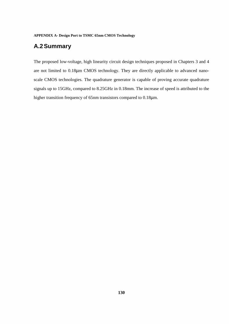
APPENDIX A- Design Port to TSMC 65nm CMOS Technology
130
A.2 Summary
The proposed low-voltage, high linearity circuit design techniques proposed in Chapters 3 and 4
are not limited to 0.18µm CMOS technology. They are directly applicable to advanced nano-
scale CMOS technologies. The quadrature generator is capable of proving accurate quadrature
signals up to 15GHz, compared to 8.25GHz in 0.18mm. The increase of speed is attributed to the
higher transition frequency of 65nm transistors compared to 0.18µm.


![Reconfiguration-based hierarchical energy management in ......HAMZEH AGHDAM et al./Turk J Elec Eng & Comp Sci References [1] Hagh MT, Aghdam FH. Smart hybrid nanogrids using modular](https://img.pdfslide.net/doc/110x75/602ea82412e4514ff372aa07/reconfiguration-based-hierarchical-energy-management-in-hamzeh-aghdam-et.jpg)