Embed Size (px)
Citation preview
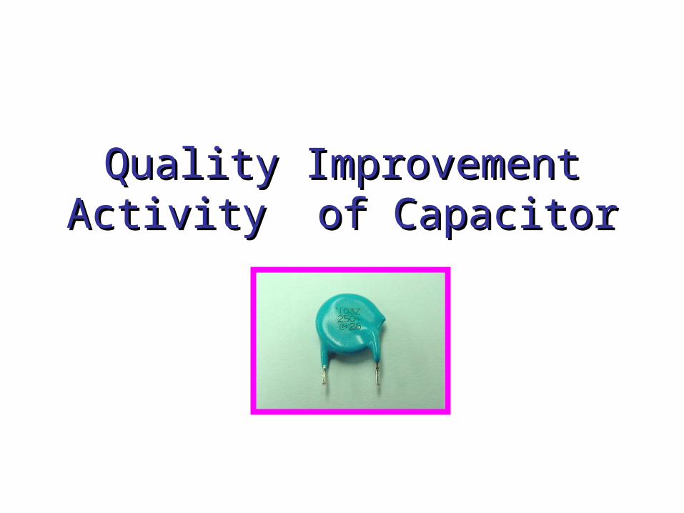
Quality Improvement Activity Quality Improvement Activity of Capacitorof Capacitor
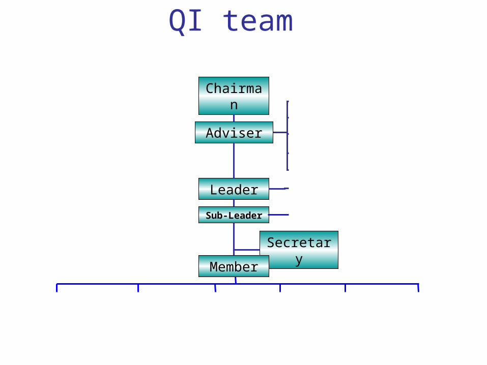
QI team
Chairman
Adviser
Leader
Secretary
Sub-Leader
Member
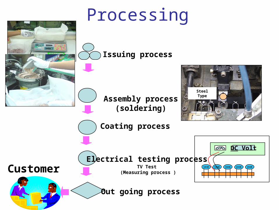
Assembly process (soldering)
Issuing process
Coating process
Electrical testing process
Out going process
Processing
Steel Type
151K 151K 151K 151K 151K
DC Volt
TV Test (Measuring process )Customer
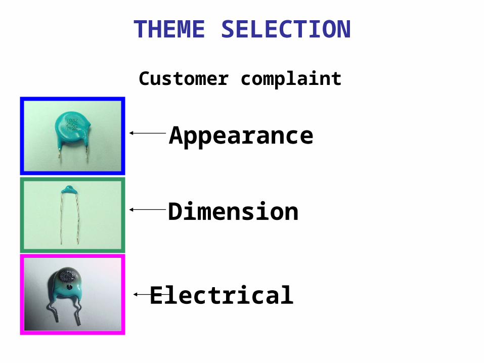
Appearance
Dimension
Electrical
Customer complaint
THEME SELECTION
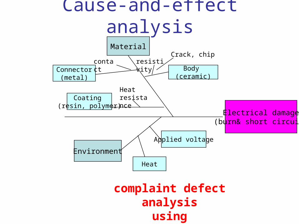
Cause-and-effect analysis
Material
Connector(metal)
Coating (resin, polymer)
contactBody
(ceramic)
Crack, chipresistivity
Heat resistance
Environment
Heat
Applied voltage
complaint defect analysisusing
dispersion C&E diagram
Electrical damage(burn& short circuit)
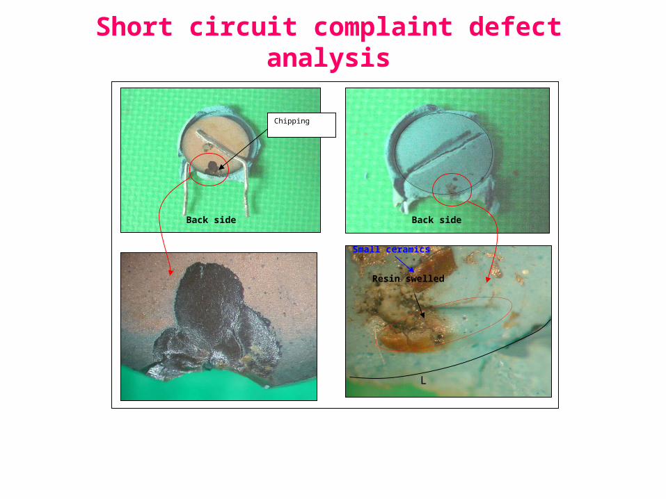
Back side Back side
Chipping
Resin swelled
Small ceramics
L
Short circuit complaint defect analysis
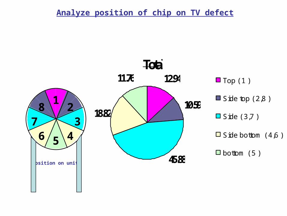
Total12.94
10.5918.82
11.76
45.88
Top ( 1 )
Side top ( 2,8 )
Side ( 3,7 )
Side bottom ( 4,6 )
bottom ( 5 )
Analyze position of chip on TV defect
Position on unit
12
3456
78
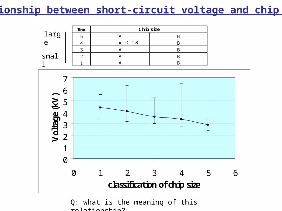
Item
5
4
3
2
1 A B
A
A
B
B
Chip size
A B
A B< 1.3
> 1.3
< 1.0
< 0.7
< 0.5
1.0 <
0.7 <
0.5 <
> 0.7
< 0.5< 0.4
< 0.3
< 0.70.5 <
0.3 <0.4 <
0
12
34
56
7
0 1 2 3 4 5 6
classification of chip size
Vol
tage
(kV
)
Relationship between short-circuit voltage and chip size
large
small
Q: what is the meaning of this relationship?
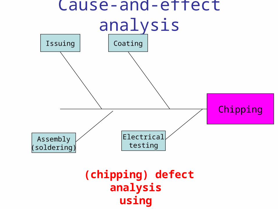
Cause-and-effect analysis
Issuing
Assembly(soldering)
Electricaltesting
Coating
(chipping) defect analysisusing
process C&E diagram
Chipping
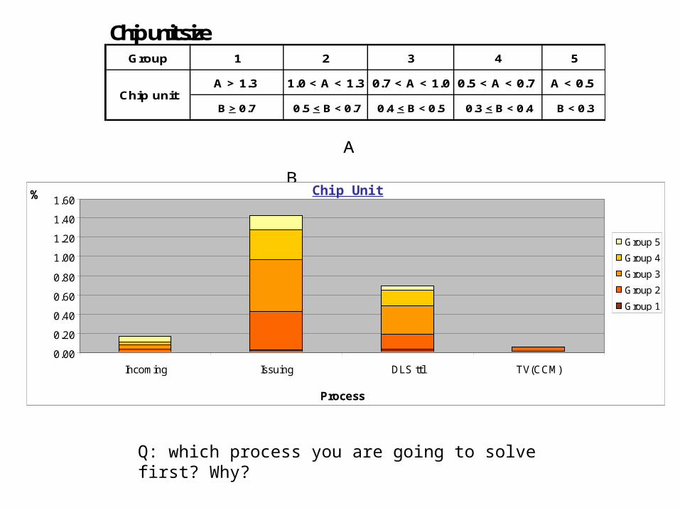
Chip unit sizeGroup 1 2 3 4 5
A > 1.3 1.0 < A < 1.3 0.7 < A < 1.0 0.5 < A < 0.7 A < 0.5
B > 0.7 0.5 < B < 0.7 0.4 < B < 0.5 0.3 < B < 0.4 B < 0.3Chip unit
A
B
0.00
0.20
0.40
0.60
0.80
1.00
1.20
1.40
1.60
Incoming Issuing DLS ttl TV(CCM)
Process
%
Group 5
Group 4
Group 3
Group 2
Group 1
Chip Unit
Q: which process you are going to solve first? Why?
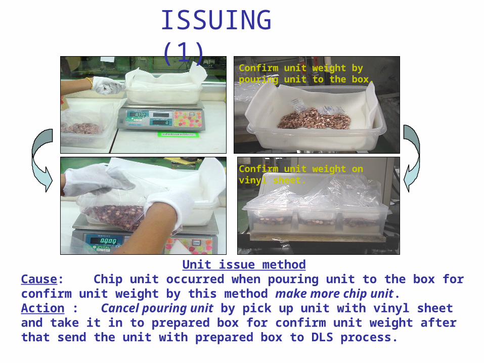
Unit issue methodCause: Chip unit occurred when pouring unit to the box for confirm unit weight by this method make more chip unit.Action : Cancel pouring unit by pick up unit with vinyl sheet and take it in to prepared box for confirm unit weight after that send the unit with prepared box to DLS process.
Confirm unit weight on vinyl sheet.
Confirm unit weight by pouring unit to the box.
ISSUING (1)
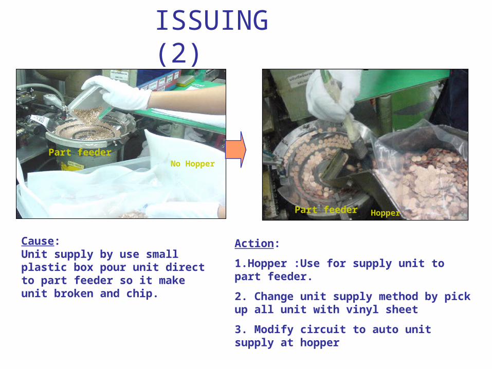
Action:
1.Hopper :Use for supply unit to part feeder.
2. Change unit supply method by pick up all unit with vinyl sheet
3. Modify circuit to auto unit supply at hopper
Cause:Unit supply by use small plastic box pour unit direct to part feeder so it make unit broken and chip.
No HopperPart feeder
HopperPart feeder
ISSUING (2)
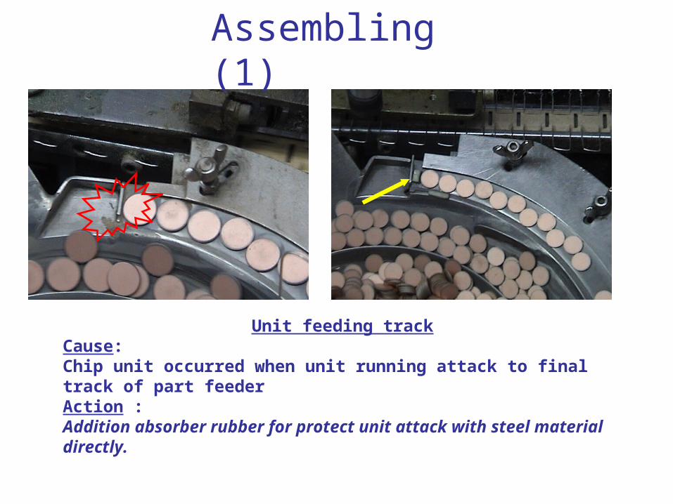
Unit feeding trackCause:Chip unit occurred when unit running attack to final track of part feederAction : Addition absorber rubber for protect unit attack with steel material directly.
Assembling (1)
Steel Type
UPE Type
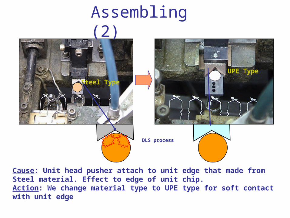
Cause: Unit head pusher attach to unit edge that made from Steel material. Effect to edge of unit chip.Action: We change material type to UPE type for soft contact with unit edge
DLS process
Assembling (2)
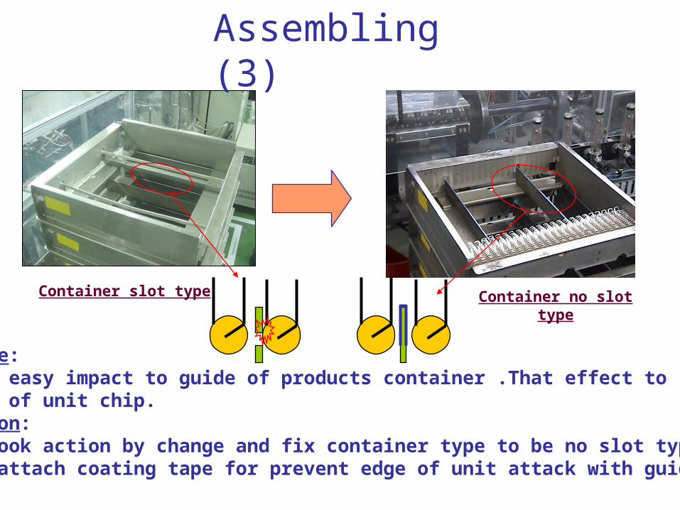
Cause:Unit easy impact to guide of products container .That effect to edge of unit chip. Action:We took action by change and fix container type to be no slot type.And attach coating tape for prevent edge of unit attack with guide.
Container slot type Container no slot type
Assembling (3)
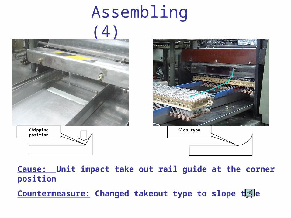
Cause: Unit impact take out rail guide at the corner position
Countermeasure: Changed takeout type to slope type
Chipping position Slop type
Assembling (4)
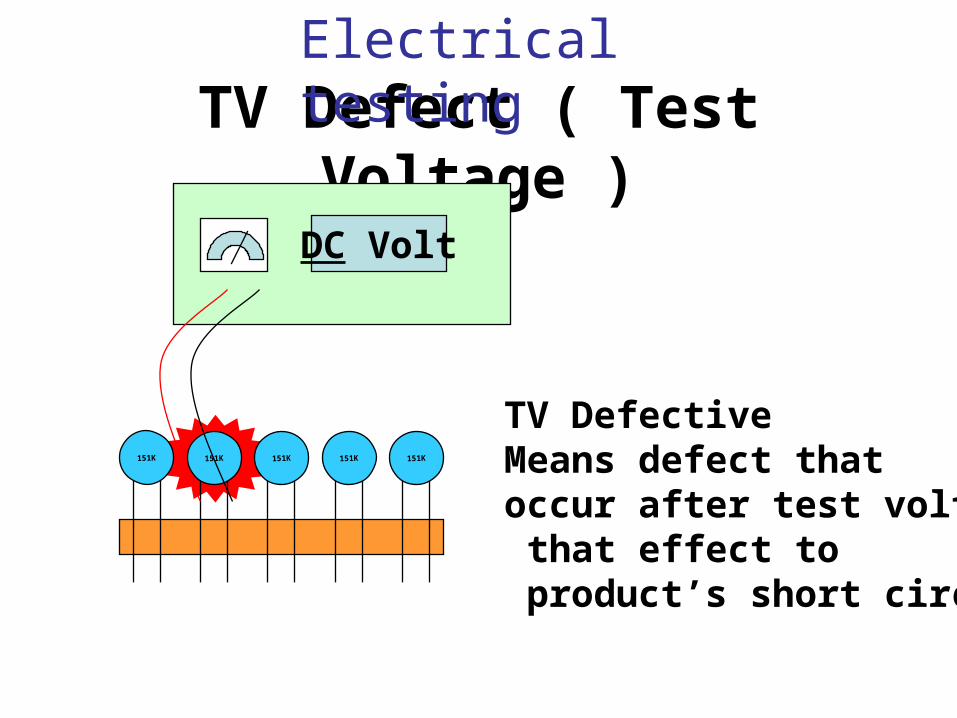
TV Defect ( Test Voltage )
151K 151K 151K 151K 151K
DC Volt
TV Defective Means defect that occur after test voltage that effect to product’s short circuit
Electrical testing
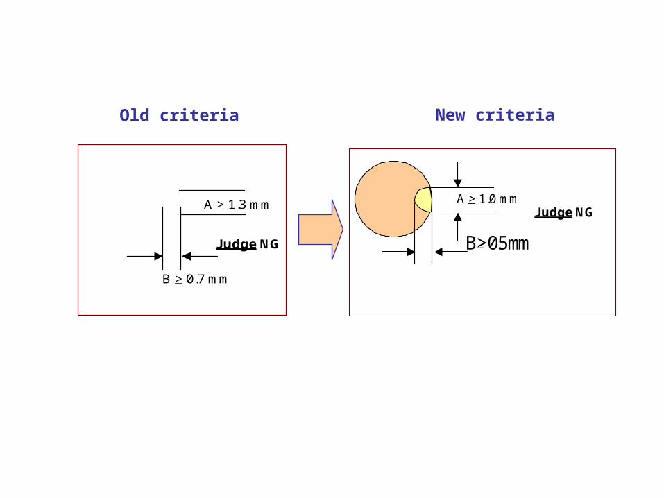
A > 1.3 mm
B > 0.7 mm
Judge NG
A > 1.3 mmA > 1.0 mm
B > 0.5 mm
Current Limit Sample
Judge NG
Old criteria New criteria
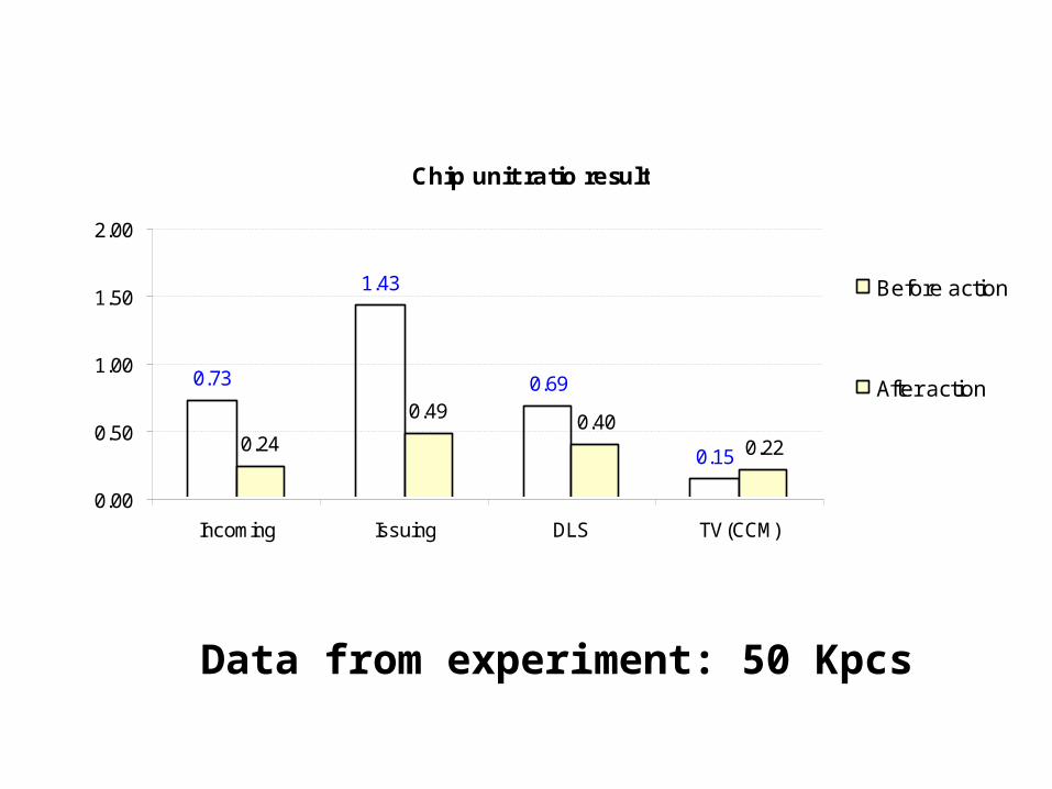
Chip unit ratio result
0.73
1.43
0.69
0.150.24
0.49 0.400.22
0.00
0.50
1.00
1.50
2.00
Incoming Issuing DLS TV(CCM)
Before action
After action
Data from experiment: 50 Kpcs
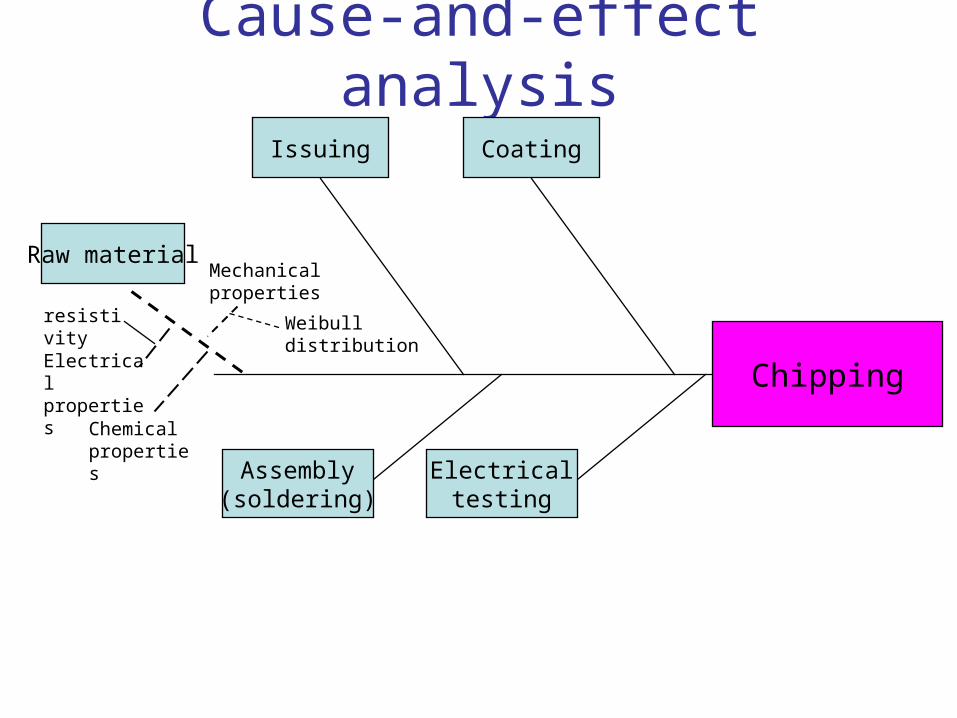
Cause-and-effect analysis
Issuing
Assembly(soldering)
Electricaltesting
Coating
Chipping
Weibull distribution
Raw materialMechanical properties
Electrical properties
resistivity
Chemical properties