Embed Size (px)
Citation preview
Copyright © 2010 by Gregory L. Moss 1
Quartus Tutorial 3 – Hierarchical Designs A step-by-step tutorial using Quartus II v9.x
by Gregory L. Moss
Example 5-1 Tutorial
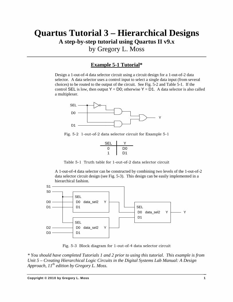
Design a 1-out-of-4 data selector circuit using a circuit design for a 1-out-of-2 data selector. A data selector uses a control input to select a single data input (from several choices) to be routed to the output of the circuit. See Fig. 5-2 and Table 5-1. If the control SEL is low, then output Y = D0; otherwise Y = D1. A data selector is also called a multiplexer.
*
Y
SEL
D0
D1
Fig. 5-2 1-out-of-2 data selector circuit for Example 5-1
SEL Y 0 D0 1 D1
Table 5-1 Truth table for 1-out-of-2 data selector circuit
A 1-out-of-4 data selector can be constructed by combining two levels of the 1-out-of-2 data selector circuit design (see Fig. 5-3). This design can be easily implemented in a hierarchical fashion.
data_sel2SELD0D1
Y
data_sel2SELD0D1
Y
data_sel2SELD0D1
Y
D0D1
D2D3
S1S0
Y
Fig. 5-3 Block diagram for 1-out-of-4 data selector circuit
* You should have completed Tutorials 1 and 2 prior to using this tutorial. This example is from Unit 5 – Creating Hierarchical Logic Circuits in the Digital Systems Lab Manual: A Design Approach, 11th edition by Gregory L. Moss.

Quartus II Hierarchical Tutorial
Copyright © 2010 by Gregory L. Moss 2
Quartus II procedures for Example 5-1
1. Start Quartus II. The main screen will open. Start the New Project Wizard by clicking the Create a New Project button on the Getting Started window. You can also start the New Project Wizard by double-clicking “Open New Project Wizard” in the expanded “Start Project” task folder in the “Full Design” Flow Tasks Pane. The New Project Wizard: Introduction window will open. Click the Next button. This example procedure will enter the hierarchical design as multiple projects. Start with the lowest level blocks and then work your way up to the top-level block. The lowest-level block in this example is the circuit in Fig. 5-2. Each different block design will be represented as a new project. Hierarchical designs may also be entered as a single project but lower level block testing is more difficult.
Start a New Design Project for the Lowest-Level Block(s)
2. The Directory, Name, Top-Level Entity dialog box opens. Use computer resources specified by your lab instructor. The working directory for this project is example5_1a. The project is named data_sel2. The Wizard will automatically copy the project name as the top-level design entity name for this project. Each project will have one top-level design entity. A new directory (folder) should be created for each separate design project. There will be many files associated with a project and they should all be placed in the same folder. Do not use duplicate design file names in a project. Click the Next button. Click Yes to create the directory.
3. The Add Files dialog box will open. This lowest-level block does not have any additional design files to add to the project, so click the Next button.
4. The Family & Device Settings dialog box opens. Use the correct device information for your specific hardware in this dialog box. Select the appropriate Family in the drop-down box. Under Target device, choose “Specific device selected in ‘Available devices’ list.” Select the target device from the list of Available devices. Click Next.
5. The EDA Tool Settings dialog box opens. There are no additional tools to use, so click Next.
6. The Summary window opens. Click Finish. Project settings may be changed in the Settings dialog box (open in the Assignments menu or with the Settings button in the tool bar).

Quartus II Hierarchical Tutorial
Copyright © 2010 by Gregory L. Moss 3
7. Open the “Create Design” task folder in the Tasks Pane (click the expand button). Double-click “Create New Design File” to open the New file dialog box. Select “Block Diagram/Schematic File” under “Design Files” and then click OK.
Create a Block Diagram/Schematic File
8. A blank worksheet on which we will draw our schematic appears. Choose “Save As” from the File menu. The file will be named data_sel2 and the file type is .bdf for schematics. Select “Add file to current project” and click Save.
9. Use the Quartus II Block Editor to draw the schematic for our project. Click the Symbol Tool button (gate symbol) on the left side of the Block Editor window (or double-click the left mouse button anywhere in the drawing area or right-click the mouse, choose “Insert” and then “Symbol”) and the Symbol dialog box will appear. Open the set of folders for Libraries, Primitives, and Logic and select a logic gate. Click OK. Repeat for all gates needed.
10. Place input and output symbols in the schematic so that you can connect logic signals to the circuit. Open the Symbol dialog box, close the logic library, open the pin library, and select input or output. Click OK.
11. Label the input and output node names by double-clicking on the default “pin_name” with the left mouse button and then typing the appropriate input or output name (see Fig. 5-2 and the diagram below) in the Pin Properties dialog box. Click OK when completed with each label. Repeat to label all input and output ports.
12. Draw the wires to make the necessary circuit connections. Point the mouse cursor at a device connection and the pointer will turn into a cross-hair, hold down the left mouse button, move the cursor towards the desired connection point, and release the mouse button. If you need more than one right-angle turn in the wire, you will need to end the wire (by releasing the button) and then continue drawing the wire from that point (by pressing the mouse button again). When you create a T intersection, connection dots are automatically inserted. Components or wires can be moved by selecting them (point and click on it once with the left mouse button) and dragging them to the desired location. To delete any part of the drawing, select the desired part and press the delete key. Save the file.

Quartus II Hierarchical Tutorial
Copyright © 2010 by Gregory L. Moss 4
13. This project will become a lower-level design block in a larger hierarchical design. Expand the “Compile Design” Task to view the compiler’s sub-tasks. Double-click the “Analysis & Synthesis” sub-task. If the schematic is a complete logic circuit, the message “Analysis & synthesis was successful” will be displayed. Remember that a successful compilation does not imply that the logic circuit is drawn correctly or will produce the desired output for an application. This only means that the circuit schematic is synthesizable (i.e., it will produce a logic circuit). Click OK.
Analysis & Synthesis
14. If you have errors, the “Analysis & synthesis was NOT successful” message will appear. Click OK and point the cursor to a red error message in the message window at the bottom of the screen and open the message menu by clicking the right mouse button. Context-sensitive help is available if you choose Help from the menu. If you choose Locate in the message menu and then choose Locate in Design File (or double-click the left mouse button on the error message), the location of the error in the design file will be highlighted. You can also return to the design file by clicking the data_sel2.bdf tab or using the Window menu or double-clicking the left mouse button on data_sel2 in the Project Navigator. Make the necessary corrections to the schematic and run Analysis & Synthesis again. You cannot continue unless you have a successful analysis!

Quartus II Hierarchical Tutorial
Copyright © 2010 by Gregory L. Moss 5
15. Verify the behavior of the circuit design with a Vector Waveform File (.vwf). Simulation inputs (called test vectors) and output signals along with other circuit nodes to be observed are specified in the Vector Waveform File. Double-click “Create New Design File” in the Task Pane. Select “Vector Waveform File” listed under “Verification/Debugging Files” in the New dialog box and click OK.
Simulate the Design
16. Save the Vector Waveform File with the same file name as the design entry file of the current project. This file should be added (see check box) to the current project in this directory (folder).
17. Specify an End Time & a Grid Size for the simulation file. You should coordinate these two time values. Generally, you will specify the End Time first and then the Grid Size. Specifying the End Time: Select a time value by determining the number of desired input test vectors and the amount of time for each input test vector. Apply all possible input signal combinations for this simple design. Open the Edit menu and choose “End Time.” Enter the time value and units in the End Time dialog box. Click OK. Specifying the Grid Size: Select a Grid Size that will allow a sufficient number of grid units in the End Time period to be able to adequately simulate this project. The Grid Size cannot be larger than the End Time. Open the Edit menu and choose “Grid Size.” Enter the time value and units in the Grid Size dialog box for Time period. Click OK. Open the View menu and choose “Fit in Window”
18. Insert the circuit nodes that are to be simulated. Open the Edit menu, choose “Insert,” and then select “Insert Node or Bus” in the submenu (or double-click in the “Name” field of the Waveform editor). The Insert Node or Bus dialog box will open. Specify the Radix as Binary in the drop-down box. Click the Node Finder button to add nodes to the Vector Waveform File.
19. In the Node Finder window, locate the input and output pins for this design by opening the drop down list for the Filter and select “Pins: all.” Click the List button to display a list of input and output pins in the Nodes Found window.
20. Select nodes from the Nodes Found list to be entered into the vwf file. There are two ways to do this. You can select the entire list by clicking the >> button or you can highlight one or more of the nodes in the Nodes Found list and click the > button. The selected nodes will then be listed in the Selected Nodes box. Click OK to return to Insert Node or Bus dialog box. Click OK again to return to Waveform Editor window.
21. To change the order in which the signal nodes will be displayed, first select the node to be moved by clicking on the node name (in the Name column) and then releasing the button. Next click again on the node name and drag it up or down while holding the mouse button down. Release the mouse button when the waveform indicator line is in the desired position.

Quartus II Hierarchical Tutorial
Copyright © 2010 by Gregory L. Moss 6
22. Create the desired input test vectors for the project simulation. We will be applying all eight possible combinations for the three circuit inputs sel d1 d0 using a binary count sequence. Edit the input waveforms by selecting a time segment on the input to be changed. Point the mouse cursor at the beginning of a time segment to be changed, hold down the left mouse button, and drag to the end of the desired time. The time segment selected will be highlighted. Multiple time segments can be selected by holding down the CTRL key while dragging through a time segment with the left mouse button pressed. Clicking the editing buttons on the left of the Waveform Editor window can change the logic levels for the selected time segments. Create the high pulses for the selected time segments by clicking on the 1 (Forcing High) button. Continue editing the input vectors by selecting appropriate time segments and clicking the 1 button. Note: If you make a mistake, select the time segment that needs to be changed back and click the 0 button. Save the vwf file.
23. Perform a functional simulation on the project to determine if our design is correct. We can also do a timing simulation, which will take into account all propagation delays for our device. To perform a functional simulation, open “Verify Design” and then “Simulate Design” tasks, double-click “Edit Settings” in the Tasks Pane. In the “Simulator Settings” dialog, open the drop down menu for “Simulation Mode” and select “Functional.” Click OK.
24. Start the simulator by double-clicking “Quartus II Simulator (Functional)” in the Tasks Pane. Click OK for the “Simulator was successful” message. If necessary, open the View menu and choose “Fit in Window” to view the entire Simulation Waveforms results.
25. Verify that the functional simulation of the project matches the desired truth table. If your simulation results are incorrect, you have an error in the design and it will be necessary to correct the bdf schematic, repeat Analysis & Synthesis, and then re-simulate. Toggle the display to Full Screen to maximize the Simulation Waveforms window (open View menu and choose “Full Screen”). Another click on “Full Screen” will return to the standard multi-window display.

Quartus II Hierarchical Tutorial
Copyright © 2010 by Gregory L. Moss 7
26. The current project will become a lower-level design block in another project. After determining that the current project functions correctly in the simulation, you will need to create a symbol for this block to be able to use it in a higher-level of the design hierarchy. First click the bdf window tab to open the schematic for this project. Open the File menu, choose “Create/Update,” and then choose “Create Symbol Files for Current File” in the sub-menu. This symbol should have the same filename as the design file but will have a bsf file extension. It will be saved in the same project folder. Click the Save button on the Create Symbol File dialog box. Click OK on the “Created Block Symbol File …” message.
Create a Symbol for the Lower-Level Block

Quartus II Hierarchical Tutorial
Copyright © 2010 by Gregory L. Moss 8
27. This hierarchical design is being entered as multiple projects. We will now work on the “top-level” project. The top-level block in this example is illustrated by the block diagram in Fig. 5-3. Each
Start a New Design Project for the Top-Level Block
different
28. The Directory, Name, Top-Level Entity dialog box opens. The name of the working directory for this new project is example5_1b. A new directory (folder) should be created for each separate design project. This will be a
block design will be represented as a new project. Lower level design blocks will be contained in this project. Double-click the “Open New Project Wizard” in the “Start Project” task folder in the Tasks Pane. The New Project Wizard will guide you in setting up another design block. The Introduction window will open. Click the Next button.
different directory name than was used for the lower-level project that we just completed. The project name is data_sel4. The project name must be different than the lower-level project. We can not use duplicate design file names in a project and the lower-level project will be contained in this new project. Click the Next button and then Yes to create the directory.

Quartus II Hierarchical Tutorial
Copyright © 2010 by Gregory L. Moss 9
29. The Add Files dialog box will open. We will now identify the files to be included in this top-level project. Click the Browse button to locate the working directory for the lower-level project.
Browse button

Quartus II Hierarchical Tutorial
Copyright © 2010 by Gregory L. Moss 10
30. Use the Select File dialog box to locate the lower-level project. Remember that it will be in a different directory (folder). Navigate to the lower-level project directory by selecting it in the “Look in” drop-down box. Select the project name by clicking it and it will appear in the File name: box. Click the Open button to return to the Add Files dialog box.
“Look in” drop-down box

Quartus II Hierarchical Tutorial
Copyright © 2010 by Gregory L. Moss 11
31. The File name for the design file of the lower-level project should appear in the box. Click the Add button to move this file name to the list of selected files to be added to the top-level project.
Lower-level project file name Add button

Quartus II Hierarchical Tutorial
Copyright © 2010 by Gregory L. Moss 12
32. We would continue to add more lower-level files to this project if necessary. Since this is the only file that is needed, click Next.
33. The Family & Device Settings dialog box opens. Use the correct device information for your specific hardware in this dialog box. Select the appropriate Family in the drop-down box. Under Target device, choose “Specific device selected in ‘Available devices’ list.” Select the target device from the list of Available devices. Click Next.
34. The EDA Tool Settings dialog box opens. There are no additional tools to use, so click Next.
35. The Summary window opens. Click Finish. This is the final New Project Wizard screen. Project settings may be changed in the Settings dialog box.
Quartus II Hierarchical Tutorial
Copyright © 2010 by Gregory L. Moss 13
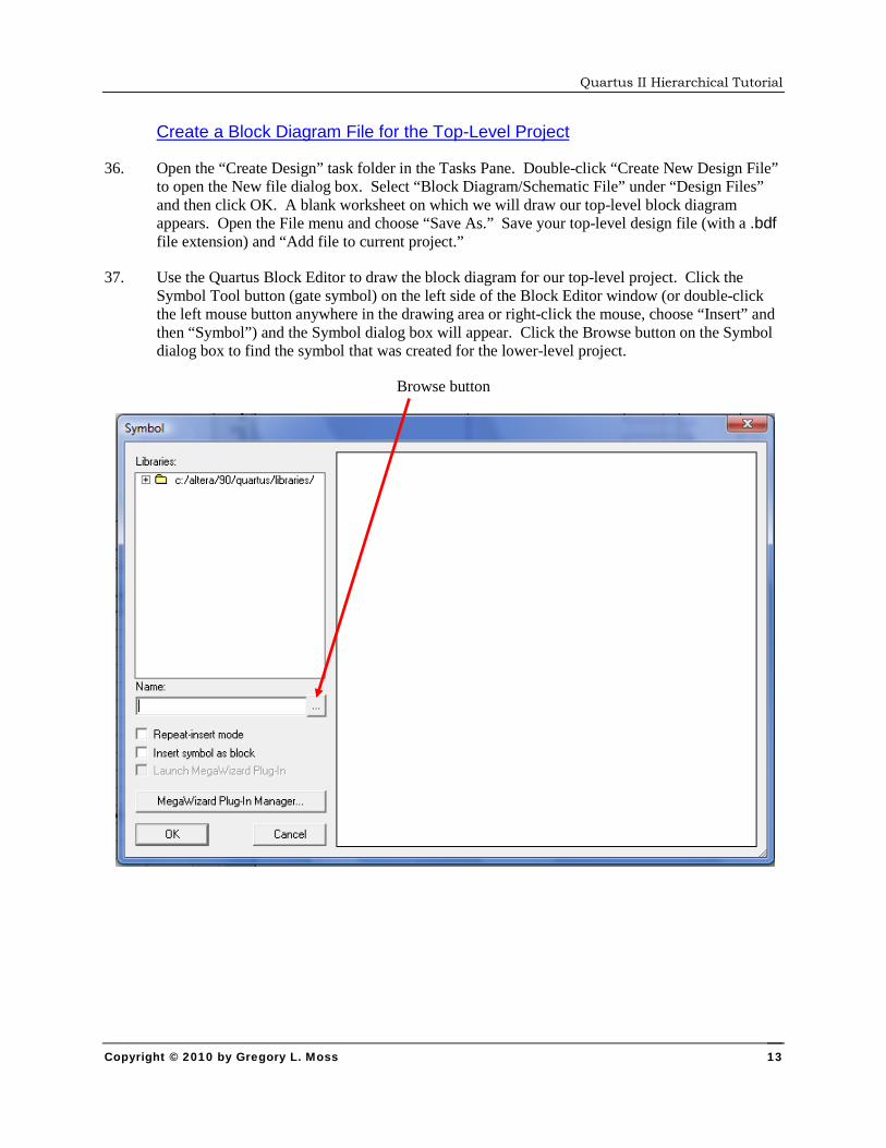
36. Open the “Create Design” task folder in the Tasks Pane. Double-click “Create New Design File” to open the New file dialog box. Select “Block Diagram/Schematic File” under “Design Files” and then click OK. A blank worksheet on which we will draw our top-level block diagram appears. Open the File menu and choose “Save As.” Save your top-level design file (with a .bdf file extension) and “Add file to current project.”
Create a Block Diagram File for the Top-Level Project
37. Use the Quartus Block Editor to draw the block diagram for our top-level project. Click the Symbol Tool button (gate symbol) on the left side of the Block Editor window (or double-click the left mouse button anywhere in the drawing area or right-click the mouse, choose “Insert” and then “Symbol”) and the Symbol dialog box will appear. Click the Browse button on the Symbol dialog box to find the symbol that was created for the lower-level project.
Browse button

Quartus II Hierarchical Tutorial
Copyright © 2010 by Gregory L. Moss 14
38. Locate the project directory of the lower-level data_sel2 file. Open the drop-down box to “Look in” and navigate through the directory list to select the project. Click the desired project directory and the lower-level project name should appear in the Name column. Note that the “Files of type:” filter is set for “Symbol Files.” Click the project name and it will be entered into the File name box. Click the Open button and return to the Symbol dialog box.
“Look in” drop-down box

Quartus II Hierarchical Tutorial
Copyright © 2010 by Gregory L. Moss 15
39. The Symbol dialog box will now show the data_sel2 symbol that was created by Quartus for the lower-level block. Since the top-level block diagram will use three copies of this lower-level block, check the “Repeat-insert mode” box. Click OK to return to the Block Editor window.

Quartus II Hierarchical Tutorial
Copyright © 2010 by Gregory L. Moss 16
40. Place 3 copies of the lower level data_sel2 symbol in the Block Editor window (see block diagram below).
41. Place input and output symbols in the schematic so that you can connect logic signals to the circuit. Open the Symbol dialog box, open the pin library, and select input or output. Click OK.
42. Label the input and output node names by double-clicking on the default “pin_name” with the left mouse button and then typing the appropriate input or output name (see Fig. 5-3 and the diagram below) in the Pin Properties dialog box. Click OK when completed with each label. Repeat to label all input and output ports.
43. Draw the wires to make the necessary circuit connections. Point the mouse cursor at a device connection and the pointer will turn into a cross-hair, hold down the left mouse button, move the cursor towards the desired connection point, and release the mouse button. If you need more than one right-angle turn in the wire, you will need to end the wire (by releasing the button) and then continue drawing the wire from that point (by pressing the mouse button again). When you create a T-intersection, connection dots are automatically inserted. Components or wires can be moved by selecting them (point and click on it once with the left mouse button) and dragging them to the desired location. To delete any part of the drawing, select the desired part and press the delete key.
44. Save the file.
45. You can view the schematic for the lower-level data_sel2 block by double-clicking on any one of the block symbols. The schematic will open in another Block Editor window.

Quartus II Hierarchical Tutorial
Copyright © 2010 by Gregory L. Moss 17
Analysis & Synthesis
46. This project is the top-level of a hierarchical design. Run (double-click) “Analysis & Synthesis” for the data_sel4 top-level project. Click OK for “Analysis & synthesis was successful” message. .
47. If you have errors, the “Analysis & synthesis was NOT successful” message will appear. Click OK and point the cursor to a red error message in the message window at the bottom of the screen and open the message menu by clicking the right mouse button. Make the necessary corrections to the schematic and run Analysis & Synthesis again. You cannot continue unless you have a successful analysis!

Quartus II Hierarchical Tutorial
Copyright © 2010 by Gregory L. Moss 18
Simulate the Top-Level Design
48. Verify the behavior of the top-level circuit design. Simulation of this project will be a bit more complicated since there are a total of 6 inputs (S1 S0 D3 D2 D1 D0) applied to the top-level circuit. That means there are 64 possible input combinations! That is probably a little more than we want (or need) to actually test the design with. So what we should do is develop a simulation strategy or plan that will adequately test the circuit design without taking the time to exhaustively test all possible combinations. The S1 S0 inputs will select which one of the D inputs (D3 D2 D1 D0) will be seen at the output Y. The table below lists some input conditions that might be chosen to test our logic circuit. We will then draw the corresponding test vectors in a Vector Waveform File (.vwf).
Selected Input Test Vectors
S1 S0 D3 D2 D1 D0 0 0 1 0 0 1 0 1 1 0 0 1 1 0 1 0 0 1 1 1 1 0 0 1 0 0 0 1 1 0 0 1 0 1 1 0 1 0 0 1 1 0 1 1 0 1 1 0 0 0 0 0 0 0 0 1 0 0 0 0 1 0 0 0 0 0 1 1 0 0 0 0 0 0 1 1 1 1 0 1 1 1 1 1 1 0 1 1 1 1 1 1 1 1 1 1 0 0 0 0 1 1 0 1 1 0 0 0 1 0 1 1 1 0 1 1 0 1 0 1

Quartus II Hierarchical Tutorial
Copyright © 2010 by Gregory L. Moss 19
49. Create a Vector Waveform File to verify the correct operation of this design by double-clicking “Create New Design File” in the Task Pane. Select “Vector Waveform File” listed under “Verification/Debugging Files” in the New dialog box and click OK.
50. Click the Save button on the toolbar (or in the File menu). Make sure that the Vector Waveform File is saved with the same file name as the design entry file of the top-level project. This *.vwf file should be added (see check box) to the current project in this directory.
51. Specify an End Time & a Grid Size for the simulation file. You should coordinate these two time values. Generally, you will specify the End Time first and then the Grid Size. Specifying the End Time: Select a time value by determining the number of desired input test vectors and the amount of time for each input test vector. Apply all possible input signal combinations for this simple design. Open the Edit menu and choose “End Time.” Enter the time value and units in the End Time dialog box. Click OK. Specifying the Grid Size: Select a Grid Size that will allow a sufficient number of grid units in the End Time period to be able to adequately simulate this project. The Grid Size cannot be larger than the End Time. Open the Edit menu and choose “Grid Size.” Enter the time value and units in the Grid Size dialog box for Time period. Click OK. Open the View menu and choose “Fit in Window”

Quartus II Hierarchical Tutorial
Copyright © 2010 by Gregory L. Moss 20
52. Next insert the circuit nodes that are to be simulated. Open the Edit menu, choose “Insert,” and then select “Insert Node or Bus” in the submenu (or double-click in the “Name” field of the Waveform editor). The Insert Node or Bus dialog box will open. Specify the Radix as Binary in the drop-down box. Open the Node Finder. Select “Pins: all” for the Filter to locate the input and output pins for this design. Click the List button to display a list of input and output pins in the Nodes Found window. Choose the desired nodes from the Nodes Found list to be entered into the vwf file. Either select the entire list by clicking the >> button or highlight one or more of the nodes in the Nodes Found list and click the > button. The selected nodes should be listed in the Selected Nodes box. Click OK to return to Insert Node or Bus dialog box. Click OK again to return to Waveform Editor window.

Quartus II Hierarchical Tutorial
Copyright © 2010 by Gregory L. Moss 21
53. The input and output nodes for the design are now inserted into the Waveform Editor window. To change the order in which the signal nodes will be displayed, first select the node to be moved by clicking on the node name (in the Name column) and then releasing the button. Next click again on the node name and drag it up or down while holding the mouse button down. Release the mouse button when the waveform indicator line is in the desired position.
54. Create the desired input test vectors for the project simulation. Edit the input waveforms by selecting a time segment on the input to be changed. Point the mouse cursor at the beginning of a time segment to be changed, hold down the left mouse button, and drag to the end of the desired time. The time segment selected will be highlighted. Multiple time segments can be selected by holding down the CTRL key while dragging through a time segment with the left mouse button pressed. Clicking the editing buttons on the left of the Waveform Editor window can change the logic levels for the selected time segments. Create the high pulses for the selected time segments by clicking on the 1 (Forcing High) button. Save the vwf file when finished.

Quartus II Hierarchical Tutorial
Copyright © 2010 by Gregory L. Moss 22
55. Perform a functional simulation on the project to determine if our design is correct. Open “Verify Design” and then “Simulate Design” tasks, double-click “Edit Settings” in the Tasks Pane (or click the Settings button in the toolbar). In the “Simulator Settings” dialog, open the drop down menu for “Simulation Mode” and select “Functional.” Click OK.
56. Perform the simulation. Start the simulator by double-clicking “Quartus II Simulator (Functional)” in the Tasks Pane. The Simulation Report will be generated by Quartus. Click OK when the “Simulator was successful” message appears. If necessary, open the View menu and choose “Fit in Window” to view the entire Simulation Waveforms results.
57. Verify that the functional simulation of the project matches the desired truth table. If your simulation results are incorrect, you have an error in the design and it will be necessary to correct the bdf schematic and re-compile (and then re-simulate to check again). You may also wish to toggle the display to Full Screen to maximize the Simulation Waveforms window (open View menu and choose “Full Screen”). Another click on “Full Screen” will return to the standard multi-window display.

Quartus II Hierarchical Tutorial
Copyright © 2010 by Gregory L. Moss 23
Manually Assign Pin Numbers for the top-level Project
58. To make manual pin assignments, open the “Assign Constraints” task folder in the Tasks Pane and double-click the “Edit Pin Assignments (Open Pin Planner)” Task (or click the Pin Planner button on the toolbar). The Pin Planner window will open. Since the design has already been compiled, the input and output nodes for this logic circuit are listed in the table at the bottom of the Pin Planner window.
59. Determine appropriate pin numbers (depends on your hardware) to use for this design. In the Pin Planner window, double-click the Location field for one of the circuit nodes. Type the desired pin number in the Location field (or scroll through the drop-down list of pin assignment choices until you come to the desired pin number and click the mouse button while pointing to that number). Then press Enter. Continue assigning pins for all inputs and outputs. The pin choices are dependent upon the specific FPGA/CPLD device and IC package that was assigned as a target device so it is critical that you have specified the correct device.

Quartus II Hierarchical Tutorial
Copyright © 2010 by Gregory L. Moss 24
Compile the Top-Level Project
60. Since we will be building this hierarchical project in hardware, we must perform a full compilation of the design. A project is compiled from the top-level and includes any lower-level design blocks that have been placed in the project’s hierarchy. The top-level project name is always given in the banner at the top of the screen. Double-click “Compile Design” in the Tasks Pane (or Click the Start Compilation button on the toolbar). After successfully compiling the project, the Project Navigator Pane will display the project’s hierarchy.

Quartus II Hierarchical Tutorial
Copyright © 2010 by Gregory L. Moss 25
Program a PLD
61. Attach the FPGA/CPLD development board to the PC using the appropriate interface cable (USB-Blaster or ByteBlaster). Also attach the proper power supply to the board. Be sure to follow any special instructions for your specific FPGA/CPLD development board.
62. Open the Programmer window by double-clicking “Program Device” in the Tasks Pane (or clicking the Programmer button on the toolbar). The programmer window should identify the correct type of hardware interface (USB-Blaster or ByteBlaster). If not, click the Hardware Setup button, select the appropriate interface hardware for your development board, & return to the Programmer window. Make sure the Program/Configure function for the programmer is selected. To prevent damage to the FPGA/CPLD, make sure that output pins have not been connected to input sources (such as logic switches). Turn on the power to the board & click the Start button in the Programmer window. When the Progress bar shows 100%, the programming is complete and the FPGA/CPLD is ready for testing. Connect lights and switches, if they are not pre-wired.
63. Test your circuit by applying some input combinations using the logic switches and monitor the resulting output on the lights. Only one of the D inputs (D3 D2 D1 D0) should control the output light for each combination of S1 S0. Does the circuit function correctly? If it does, demo your project to your lab instructor. Create a truth table to record your test results.