Embed Size (px)
Citation preview
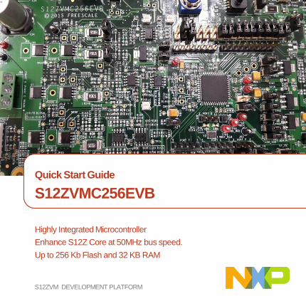
Part Number HereQuick Start Guide
Highly Integrated Microcontroller
Enhance S12Z Core at 50MHz bus speed.
Up to 256 Kb Flash and 32 KB RAM
S12ZVM DEVELOPMENT PLATFORM
S12ZVMC256EVB
1
Quick Start Guide
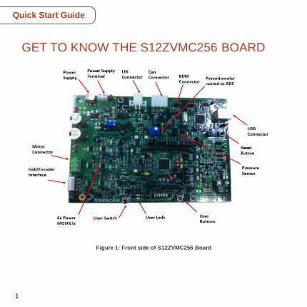
GET TO KNOW THE S12ZVMC256 BOARD
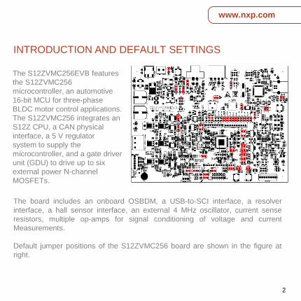
Figure 1: Front side of S12ZVMC256 Board
2
www.nxp.com
The S12ZVMC256EVB features
the S12ZVMC256
microcontroller, an automotive
16-bit MCU for three-phase
BLDC motor control applications.
The S12ZVMC256 integrates an
S12Z CPU, a CAN physical
interface, a 5 V regulator
system to supply the
microcontroller, and a gate driver
unit (GDU) to drive up to six
external power N-channel
MOSFETs.
INTRODUCTION AND DEFAULT SETTINGS
The board includes an onboard OSBDM, a USB-to-SCI interface, a resolver
interface, a hall sensor interface, an external 4 MHz oscillator, current sense
resistors, multiple op-amps for signal conditioning of voltage and current
Measurements.
Default jumper positions of the S12ZVMC256 board are shown in the figure at
right.
3
Quick Start Guide
SOFTWARE TOOLS
INSTALLATION
NXP’s CodeWarrior development
studio for MCUs integrates the
development tools for several
architectures, including the S12Z
architecture, into a single product
based on the Eclipse open
development platform. Eclipse
offers an excellent framework for
building software development
environments and is a standard
framework used by many
embedded software vendors.
STEP-BY-STEP
INSTRUCTIONS
The latest version of CodeWarrior for
MCUs (Eclipse IDE) can be downloaded
from www.nxp.com/CodeWarrior.
The project file contains a CodeWarrior project
to exercise the different modules of the
S12ZVMC microcontroller family, including
the ADC, GDU, PTU, PMF, TIM, SCI and
LIN modules.
Launch the Demo
Program2
1
4
www.nxp.com
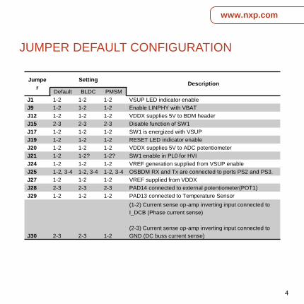
JUMPER DEFAULT CONFIGURATION
Jumpe
r
SettingDescription
Default BLDC PMSM
J1 1-2 1-2 1-2 VSUP LED indicator enable
J9 1-2 1-2 1-2 Enable LINPHY with VBAT
J12 1-2 1-2 1-2 VDDX supplies 5V to BDM header
J15 2-3 2-3 2-3 Disable function of SW1
J17 1-2 1-2 1-2 SW1 is energized with VSUP
J19 1-2 1-2 1-2 RESET LED indicator enable
J20 1-2 1-2 1-2 VDDX supplies 5V to ADC potentiometer
J21 1-2 1-2? 1-2? SW1 enable in PL0 for HVI
J24 1-2 1-2 1-2 VREF generation supplied from VSUP enable
J25 1-2, 3-4 1-2, 3-4 1-2, 3-4 OSBDM RX and Tx are connected to ports PS2 and PS3.
J27 1-2 1-2 1-2 VREF supplied from VDDX
J28 2-3 2-3 2-3 PAD14 connected to external potentiometer(POT1)
J29 1-2 1-2 1-2 PAD13 connected to Temperature Sensor
J30 2-3 2-3 1-2
(1-2) Current sense op-amp inverting input connected to
I_DCB (Phase current sense)
(2-3) Current sense op-amp inverting input connected to
GND (DC buss current sense)
5
www.nxp.com
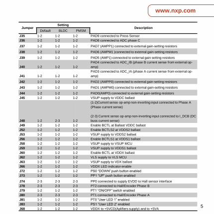
JumperSetting
DescriptionDefault BLDC PMSM
J35 1-2 1-2 1-2 PAD9 connected to Press Sensor
J36 1-2 1-2 1-2 PAD8 connected to ADC phase C
J37 1-2 1-2 1-2 PAD7 (AMPP1) connected to external gain-setting resistors
J38 1-2 1-2 1-2 PAD6 (AMPM1 )connected to external gain-setting resistors
J39 1-2 1-2 1-2 PAD5 (AMP1) connected to external gain setting resistors
J40 1-2 1-2 1-2
PAD4 connected to ADC_IB (phase B current sense from external op-
amp)
J41 1-2 1-2 1-2
PAD3 connected to ADC_IA (phase A current sense from external op-
amp)
J42 1-2 1-2 1-2 PAD2 (AMPP0) connected to external gain-setting resistors
J43 1-2 1-2 1-2 PAD1 (AMPM0) connected to external gain-setting resistors
J44 1-2 1-2 1-2 PAD0(AMP0) connected to external gain-setting resistors
J45 1-2 1-2 1-2 VSUP supply to VDDC ballast
J48 1-2 2-3 1-2
(1-2)Current sense op-amp non-inverting input connected to Phase A
(Phase current sense)
(2-3) Current sense op-amp non-inverting input connected to I_DCB (DC
buss current sense)
J49 1-2 1-2 1-2 Enable BCTL at Ballast VDDC ballast
J52 1-2 1-2 1-2 Enable BCTLS2 at VDDS2 ballast
J53 1-2 1-2 1-2 VSUP supply to VDDS2 ballast
J56 1-2 1-2 1-2 Enable BCTLS1 at VDDS1 ballast
J58 1-2 1-2 1-2 VSUP supply to VSUP MCU
J59 1-2 1-2 1-2 VSUP supply to VDDS1 ballast
J60 1-2 1-2 1-2 Enable BCTL at VDDX ballast
J62 1-2 1-2 1-2 VLS supply to VLS MCU
J63 1-2 1-2 1-2 VSUP supply to VDX ballast
J66 1-2 1-2 1-2 VDDX LED indicator enable
J72 1-2 1-2 1-2 PS0 “DOWN” push button enabled
J73 1-2 1-2 1-2 PP1 “UP” push button enabled
J74 2-3 2-3 2-3 PP0 connected to supply EVDD to Hall sensor interface
J78 2-3 2-3 2-3 PT2 connected to Hall/Encoder Phase B
J79 1-2 1-2 1-2 PT1 “ON/OFF” switch enabled
J80 2-3 2-3 2-3 PT1 connected to Hall/Encoder Phase A
J81 1-2 1-2 1-2 PT0 “User LED 1” enabled
J83 1-2 1-2 1-2 PS1 “User LED 2” enabled
J68 1-2 1-2 1-2 VDDX to +5VCD(Aplifiers supply) and to +5VA
6
www.nxp.com
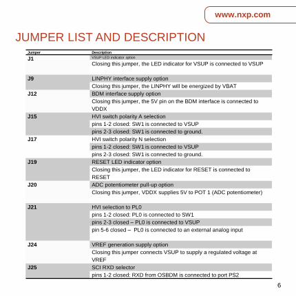
JUMPER LIST AND DESCRIPTIONJumper Description
J1 VSUP LED indicator option
Closing this jumper, the LED indicator for VSUP is connected to VSUP
J9 LINPHY interface supply option
Closing this jumper, the LINPHY will be energized by VBAT
J12 BDM interface supply option
Closing this jumper, the 5V pin on the BDM interface is connected to
VDDX
J15 HVI switch polarity A selection
pins 1-2 closed: SW1 is connected to VSUP
pins 2-3 closed: SW1 is connected to ground.
J17 HVI switch polarity N selection
pins 1-2 closed: SW1 is connected to VSUP
pins 2-3 closed: SW1 is connected to ground.
J19 RESET LED indicator option
Closing this jumper, the LED indicator for RESET is connected to
RESET
J20 ADC potentiometer pull-up option
Closing this jumper, VDDX supplies 5V to POT 1 (ADC potentiometer)
J21 HVI selection to PL0
pins 1-2 closed: PL0 is connected to SW1
pins 2-3 closed – PL0 is connected to VSUP
pin 5-6 closed – PL0 is connected to an external analog input
J24 VREF generation supply option
Closing this jumper connects VSUP to supply a regulated voltage at
VREF
J25 SCI RXD selector
pins 1-2 closed: RXD from OSBDM is connected to port PS2

7
www.nxp.com
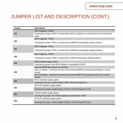
Jumper Description
J27 VREF selector
pins 1-2 closed – VREF supplied from VDDX
pins 2-3 closed – VREF supplied from the VREF2 regulator
J28 ADC mapping – PAD14
pins 1-2 closed – Connects PAD14 to POS_SIN
pins 2-3 closed – Connects PAD14 to external potentiometer
J29 ADC mapping – PAD13
pins 1-2 closed – Connects PAD13 to temperature sensor output
pins 2-3 closed – Connects PAD13 to external potentiometer
J30 Internal AMP0 input selector (inverting)
pins 1-2 closed – Connects DC Bus to the internal AMP0 inverting input (Phase A current sense)
pins 2-3 closed – Connects Ground to the internal AMP0 inverting input (DC Bus current sense)
J35 ADC mapping – PAD9
Closing this jumper, PAD9 is connected to Pres sensor output
J36 ADC mapping – PAD8
Closing this jumper, PAD8 is connected to ADC_IC(phase C current sense from external op-amp)
J37 ADC mapping – PAD7
Closing this jumper, PAD7 is connected to AMPP1 external gain-setting resistors
J38 ADC mapping – PAD6
Closing this jumper, PAD6 is connected to AMPM1 external gain-setting resistors
J39 ADC mapping – PAD5
Closing this jumper, PAD5 is connected to AMP1 external gain-setting resistors
J40 ADC mapping – PAD4
Closing this jumper, PAD4 is connected to ADC_IB (phase B current sense from external op-amp)
JUMPER LIST AND DESCRIPTION (CONT.)
8
www.nxp.com
JUMPER LIST AND DESCRIPTION (CONT.)
Jumper Description
J41
ADC mapping – PAD3
Closing this jumper, PAD3 is connected to ADC_IA (phase A current sense from external op-
amp)
J42
ADC mapping – PAD2
Closing this jumper, PAD2 is connected to AMPP0 external gain-setting resistors
J43
ADC mapping – PAD1
Closing this jumper, PAD1 is connected to AMPM0 external gain-setting resistors
J44
ADC mapping – PAD0
Closing this jumper, PAD0 is connected to AMP0 external gain-setting resistors
J45VDDC ballast supply option
Closing this jumper, the VDDC ballast is connected to VSUP
J48
Internal AMP0 input selector (inverting)
pins 1-2 closed – Connects DC Bus to the internal AMPP0 inverting input (Phase A current
sense)
pins 2-3 closed – Connects Ground to the internal AMPP0 inverting input (DC Bus current
sense)
J49BCTL interface supply option
Closing this jumper, enable ballast VDDC-VSUP through BCTL
J52
BCTLS2 interface supply option
Closing this jumper, enable ballast VDDS2-VSUP through BCTLS2
J53VDDS2 ballast supply option
Closing this jumper, the VDDS2 ballast is connected to VSUP
J56
BCTLS1 interface supply option
Closing this jumper, enable ballast VDDS1-VSUP through BCTLS1
9
www.nxp.com
JUMPER LIST AND DESCRIPTION (CONT.)
Jumper Description
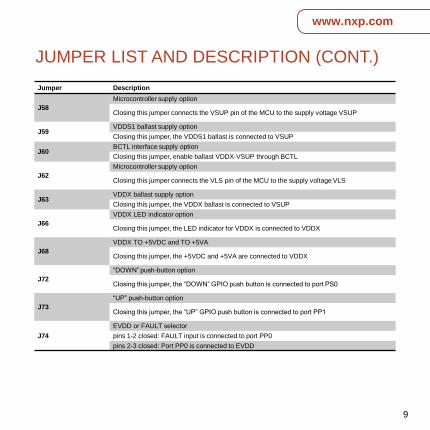
J58
Microcontroller supply option
Closing this jumper connects the VSUP pin of the MCU to the supply voltage VSUP
J59VDDS1 ballast supply option
Closing this jumper, the VDDS1 ballast is connected to VSUP
J60BCTL interface supply option
Closing this jumper, enable ballast VDDX-VSUP through BCTL
J62
Microcontroller supply option
Closing this jumper connects the VLS pin of the MCU to the supply voltage VLS
J63VDDX ballast supply option
Closing this jumper, the VDDX ballast is connected to VSUP
J66
VDDX LED indicator option
Closing this jumper, the LED indicator for VDDX is connected to VDDX
J68
VDDX TO +5VDC and TO +5VA
Closing this jumper, the +5VDC and +5VA are connected to VDDX
J72
“DOWN” push-button option
Closing this jumper, the “DOWN” GPIO push button is connected to port PS0
J73
“UP” push-button option
Closing this jumper, the “UP” GPIO push button is connected to port PP1
J74
EVDD or FAULT selector
pins 1-2 closed: FAULT input is connected to port PP0
pins 2-3 closed: Port PP0 is connected to EVDD
10
www.nxp.com
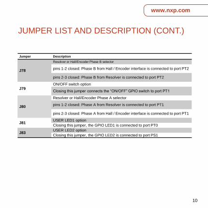
Jumper Description
J78
Resolver or Hall/Encoder Phase B selector
pins 1-2 closed: Phase B from Hall / Encoder interface is connected to port PT2
pins 2-3 closed: Phase B from Resolver is connected to port PT2
J79ON/OFF switch option
Closing this jumper connects the “ON/OFF” GPIO switch to port PT1
J80
Resolver or Hall/Encoder Phase A selector
pins 1-2 closed: Phase A from Resolver is connected to port PT1
pins 2-3 closed: Phase A from Hall / Encoder interface is connected to port PT1
J81USER LED1 option
Closing this jumper, the GPIO LED1 is connected to port PT0
J83USER LED2 option
Closing this jumper, the GPIO LED2 is connected to port PS1
JUMPER LIST AND DESCRIPTION (CONT.)
11
www.nxp.com
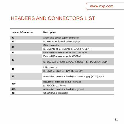
HEADERS AND CONNECTORS LIST
Header / Connector Description
J2 Alternative power supply connector
J3 DC connector for wall power supply
J4CAN connector
(1. MSCAN_H, 2. MSCAN_L, 3. Gnd, 4. VBAT)
J5 External BDM connector for S12ZVM MCU
J6
External BDM connector for OSBDM
(1. BKGD, 2. Ground, 3. PDO, 4. RESET, 5. PDOCLK, 6. VDD)
J7LIN connector
(1. GND, 2. GND, 3. +12V [HD], 4. LIN)
J8 Alternative connector (blade) for power supply (+12V) input
J10Header for extended debug interface
(1. PDOCLK, 2. PDO)
J13 Alternative connector (blade) for ground
J14 OSBDM USB connector
12
www.nxp.com
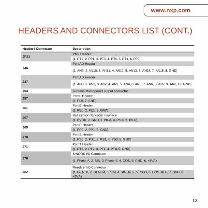
Header / Connector Description
JP21PMF Header
(1. PT2, 2. PP1, 3. PT3, 4. PT0, 5. PT1, 6. PP0)
J46
Port AD Header
(1. AN9, 2. AN10, 3. AN11, 4. AN12, 5. AN13, 6. AN14, 7. AN15, 8. GND)
J47
Port AD Header
(1. AN0, 2. AN1, 3. AN2, 4. AN3, 5. AN4, 6. AN5, 7. AN6, 8. AN7, 9. AN8, 10. GND)
J54 3-Phase Motor power output connector
J57Port L Header
(1. PL0, 2. GND)
J61Port E Header
(1. PE0, 2. PE1, 3. GND)
J67Hall sensor / Encoder interface
(1. EVDD, 2. GND, 3. Ph-A, 4. Ph-B, 5. Ph-C)
J69Port P Header
(1. PP0, 2. PP1, 3. GND)
J70Port S Header
(1. PS0, 2. PS1, 3. PS2, 4. PS3, 5. GND)
J71Port T Header
(1. PT3, 2. PT2, 3. PT1, 4. PT0, 5. GND)
J76
SINCOS I/O Connector
(1. Phase A, 2. SIN, 3. Phase B, 4. COS, 5. GND, 6. +5VA)
J82
Resolver I/O Connector
(1. GEN_P, 2. GEN_M, 3. SIN, 4. SIN_REF, 5. COS, 6. COS_REF, 7. GND, 8.
+5VA)
HEADERS AND CONNECTORS LIST (CONT.)
13
www.nxp.com
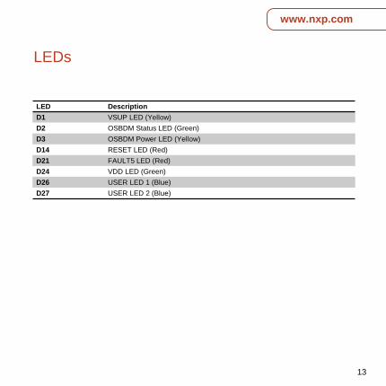
LEDs
LED Description
D1 VSUP LED (Yellow)
D2 OSBDM Status LED (Green)
D3 OSBDM Power LED (Yellow)
D14 RESET LED (Red)
D21 FAULT5 LED (Red)
D24 VDD LED (Green)
D26 USER LED 1 (Blue)
D27 USER LED 2 (Blue)
www.nxp.com
NXP and the NXP logo are trademarks of NXP B.V. All other product or service names are the property of their
respective owners. © 2016 NXP B.V.
SUPPORTVisit www.nxp.com/support for a list of
phonenumbers within your region.
WARRANTYVisit www.nxp.com/warranty for complete
warranty information.
Get Started
Download installation software
and documentation under
“Jump Start Your Design” at
nxp.com/XXXXXXXXX.
Document Number: XXXXXXXXX REV 0
Download installation software
and documentation under “Jump
Start Your Design” at
nxp.com/S12ZVMC256EVB.
Get Started