Embed Size (px)
Citation preview

Quick Tour of Logic Synthesis
Sungho Kang
Yonsei University

2CS&RSOC YONSEI UNIVERSITY
Outline
Simple Case Conversion CircuitFirst RefinementThe Transform BlockThe Command InterpreterTechnology Mapping

3CS&RSOC YONSEI UNIVERSITY
Simple CCThe LUNC Circuit
LUNC = “Lower case”, “Upper case”, “No conversion”,or “Change case” conversion circuit
8 8
ckreset
LUNC

4CS&RSOC YONSEI UNIVERSITY
Simple CCLUNC Interface
8 8
ckreset
LUNC
Input: 8-bit ASCII code of an alphanumeric character
Output: Case conversion of the input character:^[L => Convert to Lower case^[U => Convert to Upper case^[N => No conversion^[C => Change case

5CS&RSOC YONSEI UNIVERSITY
Simple CCASCII Codes
A=0x41=65=01000001 B=0x42=66=01000010 … a=0x61=97=01100001 b=0x62=98=01100010 …
Note Only change is in bit 5, soCode(a) = Code(A) +32
22
5
4
MHex
6CS&RSOC YONSEI UNIVERSITY
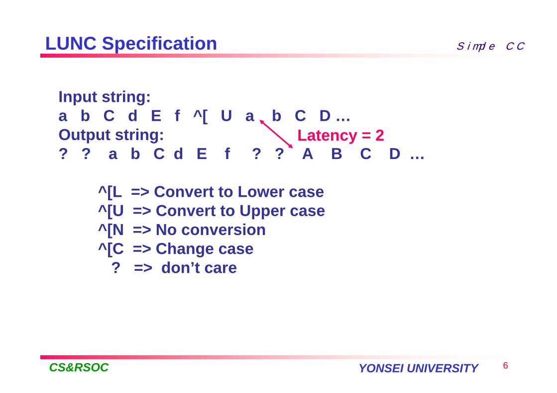
Simple CCLUNC Specification
Input string:a b C d E f ^[ U a b C D …Output string:? ? a b C d E f ? ? A B C D …
^[L => Convert to Lower case^[U => Convert to Upper case^[N => No conversion^[C => Change case
? => don’t care
Latency = 2

7CS&RSOC YONSEI UNIVERSITY
RefinementLUNC Block Diagram2 registers in datapath, solatency is 2 cycles
Controller FSM

8CS&RSOC YONSEI UNIVERSITY
Transform BlockFirst Refinement
The first step is to separate the data processing from the control
A command interpreter block (CmdInt), which parses the escape sequences and decides the state of the circuit accordingly, and a transformation block (Transform), which actually performs the case conversionThere are also an input and an output register, which determine the latency of the circuit
Defining the top level block diagram goes under the name of high level or architectural designHDL is used to describe both structure of a circuit and its behavior

9CS&RSOC YONSEI UNIVERSITY
Transform BlockTransform Block
Procedure TRANSFORM (Rin,Lcmd,Ucmd,Ncmd,Ccmd) {if (Lcmd)
{ mux = TOLOWER(Rin) }else if (Ucmd)
{ mux = TOUPPER(Rin) }else if(Ncmd)
{ mux = Rin }else if(Ccmd)
{ mux = CHANGECASE(Rin) }return(mux)
}
Behavioral Description of combinational logic:

10CS&RSOC YONSEI UNIVERSITY
Transform BlockTransform Block
RemarksA relatively high level description is easy to read and writeCalling the output MUX suggests that we can translate the IF-THEN-ELSE statement into a multiplexer
A straightforward translation of the initial description into a circuit yields an implementation that is far from optimal
However optimization techniques can be used to improve the draft circuit

11CS&RSOC YONSEI UNIVERSITY
Transform BlockTransform Block Diagram
Simple translation

12CS&RSOC YONSEI UNIVERSITY
Transform BlockTransform Block Diagram
• This implementation is clearly correct, but inelegant, since LC, UC, CC done every cycle
• Synthesis tool reduces the chip area from 606 literals to 12 literals, if the don’t care conditions are specified
• Then we show that a clever,but not so obviously correct,design can implement this function in 12 literals directly.

13CS&RSOC YONSEI UNIVERSITY
Transform BlockThe ChangeCase Block
Rin
32 +/-
isUC
res
/8
/8
Procedure CHANGECASE(Rin) { if (isUC(Rin))
{ res = Rin + 32 }else
{ res = Rin – 32 }return (res)
}
The ASCII code for the lower character can be obtained from that of the uppercase character by adding 32
ToLower and ToUpper functions can be implemented with an adder and a subtracter, respectively
14CS&RSOC YONSEI UNIVERSITY
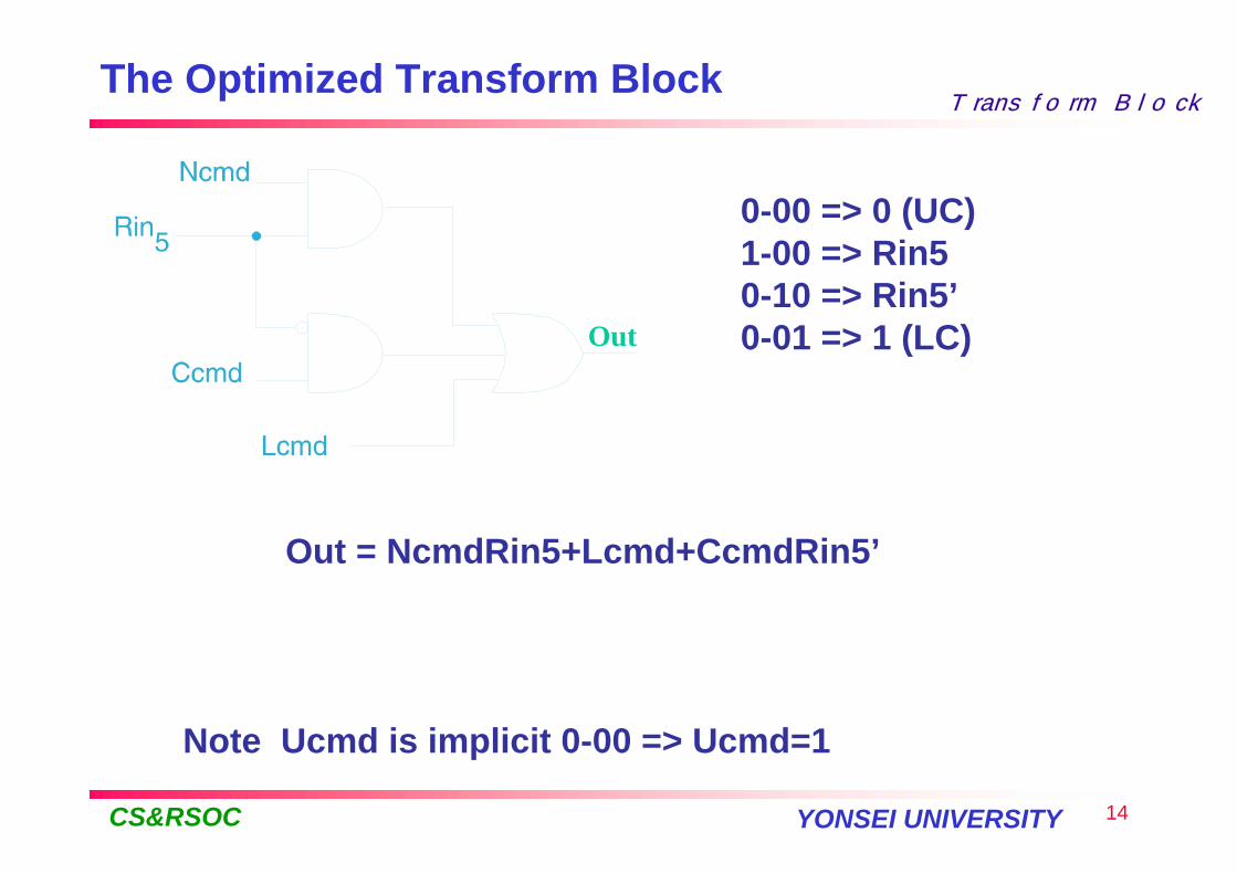
Transform BlockThe Optimized Transform Block
0-00 => 0 (UC)1-00 => Rin50-10 => Rin5’0-01 => 1 (LC)
Note Ucmd is implicit 0-00 => Ucmd=1
Out
Out = NcmdRin5+Lcmd+CcmdRin5’
15CS&RSOC YONSEI UNIVERSITY
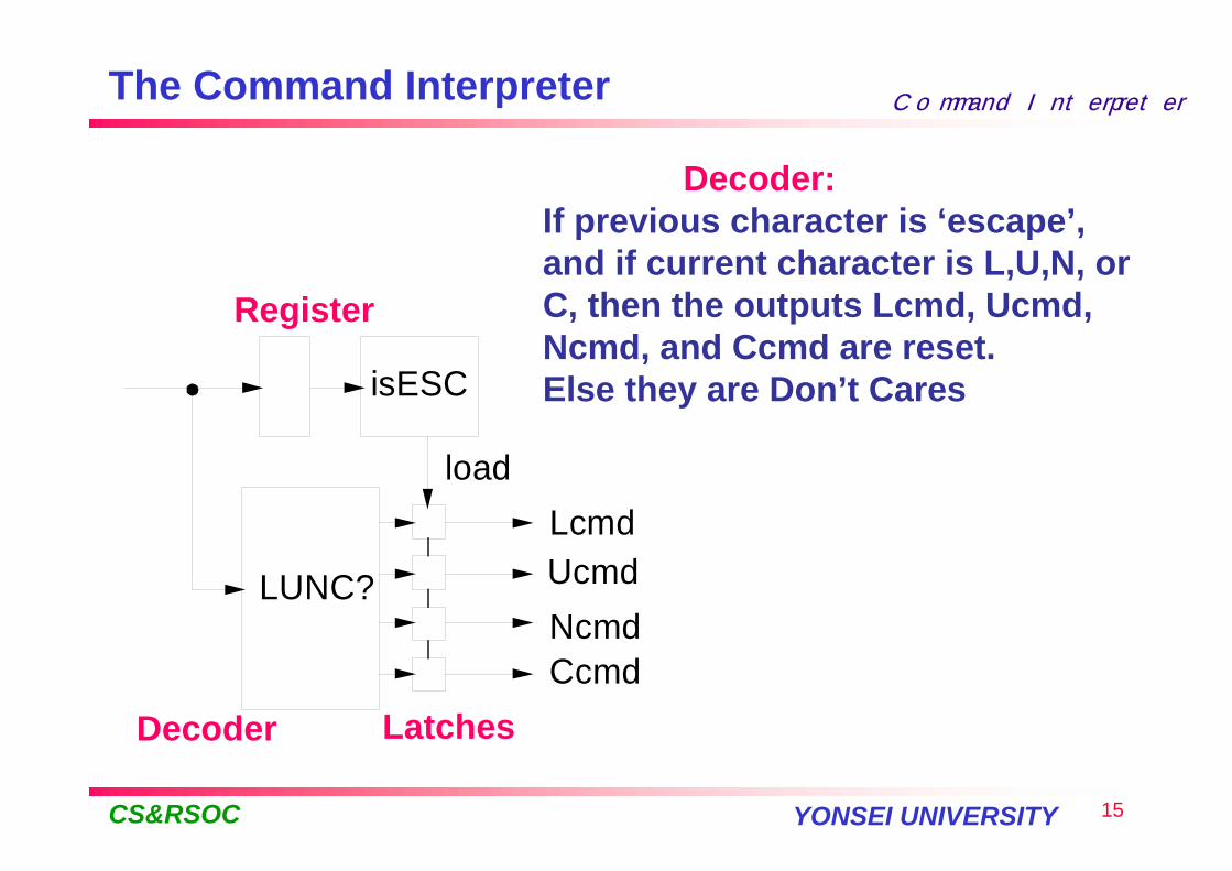
Command InterpreterThe Command Interpreter
LUNC?
isESC
LcmdUcmdNcmdCcmd
load
Latches
Register
Decoder
Decoder:If previous character is ‘escape’,and if current character is L,U,N, or C, then the outputs Lcmd, Ucmd, Ncmd, and Ccmd are reset. Else they are Don’t Cares

16CS&RSOC YONSEI UNIVERSITY
Command Interpreter
isESC(Reg) = isSame(Reg, ESC)
Procedure lunc? (Rin) {if(Rin = L) Lcmd=1, Ucmd=Ncmd=Ccmd=0else if (Rin = U) Ucmd=1, Lcmd=Ncmd=Ccmd=0 else if (Rin = N) Ncmd=1, Lcmd=Ucmd=Ccmd=0 else if (Rin = C) Ccmd=1, Lcmd=Ucmd=Ccmd=0 else Lcmd=Ucmd=Ncmd=Ccmd=Don't~Carereturn (Lcmd, Ucmd, Ncmd, Ccmd)
}
The Command Interpreter

17CS&RSOC YONSEI UNIVERSITY
Command InterpreterComparison For Equality
A7B7
A0B0
A7
A0
A=B
A=escape=0x1b=27

18CS&RSOC YONSEI UNIVERSITY
Command InterpreterDistinguishing L,U,N,C
L = 0x4C = 01001100 = 74U = 0x55 = 01010101 = 85N = 0x4E = 01001110 = 78C = 0x43 = 01000011 = 67
The last 2 bits are sufficient for distinguishing L,U,N,C
Everything else is don’t care
isL
isN
isC
Two Least significant bits
A1A0
Note that isC is not needed because of the “One Hot”assumption

19CS&RSOC YONSEI UNIVERSITY
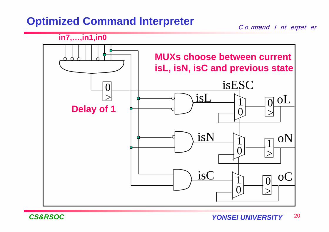
Command InterpreterDistinguishing L,U,N,C
We can considerably reduce the number of flip-flops by a simple device
Instead of storing each input to test whether it is an ‘escape’ at the next clock cycle, we can test each input character as soon as we see it, and then store the result of the test
Such a transformation is called a retiming of the circuit
20CS&RSOC YONSEI UNIVERSITY
Command InterpreterOptimized Command Interpreter
in7,…,in1,in0
0> 1
0
10
10
0>
1>
0>
isESCisL
isN
isC
oL
oN
oC
Delay of 1
MUXs choose between currentisL, isN, isC and previous state

21CS&RSOC YONSEI UNIVERSITY
Command Interpreter
reg8 reg8
Lcmd
Ncmd
Ccmd
x7,…x1,x0
i7
i0
x7
x0
o7
o0
x5
b5
CI
TB
LUNC
Only isEsc isdelayed
Overall Latency of 2

22CS&RSOC YONSEI UNIVERSITY
Technology MappingTechnology Mapping
SynthesisTranslationOptimizationTechnology mapping
Technology dependentTechnology independent