Embed Size (px)
Citation preview

Logic synthesis and Place and Route Tutorial Page 1
IC Design and Test Portland State January 2011
Laboratory University
Standard Cell ASIC Design flow: A designer uses predesigned logic cells such as AND gate, NOR gate, etc.
These gates are called Standard Cells. The advantage of Standard Cell ASIC’s is that the designers save
time, money and reduce the risk by using a predesigned and pre-tested Standard Cell Library. We will be
using Cadence RTL compiler to synthesize our design. Logic synthesis is a process by which an abstract
form of desired circuit behavior, typically register transfer level (RTL), is turned into a design
implementation in terms of logic gates. Common examples of this process include synthesis of HDLs,
including VHDL and Verilog. Logic synthesis is one aspect of electronic design automation. After logic
synthesis, in a typical ASIC design, a Place and Route tool is used to place the standard cells and then
route the nets between them and produce an optimized design. We will be using Cadence Soc
Encounter to place and route our design. This tutorial will help you to learn a typical ASIC design flow.
We will be using the following flow in our Labs.
Build the Schematic
of Design using
Virtuoso
Generate a HDL
netlist
Logic Synthesis
Place and Route
Simulate for
rise and fall
times and
Propagation
delays
Import the Placed n
Routed Design in
Virtuoso
Run DRC and LVS
Extract the design for
parasitics and
generate a netlist
Simulate for
rise and fall
times and
Propagation
delays
Logic synthesis and Place and Route Tutorial Page 2
IC Design and Test Portland State January 2011
Laboratory University
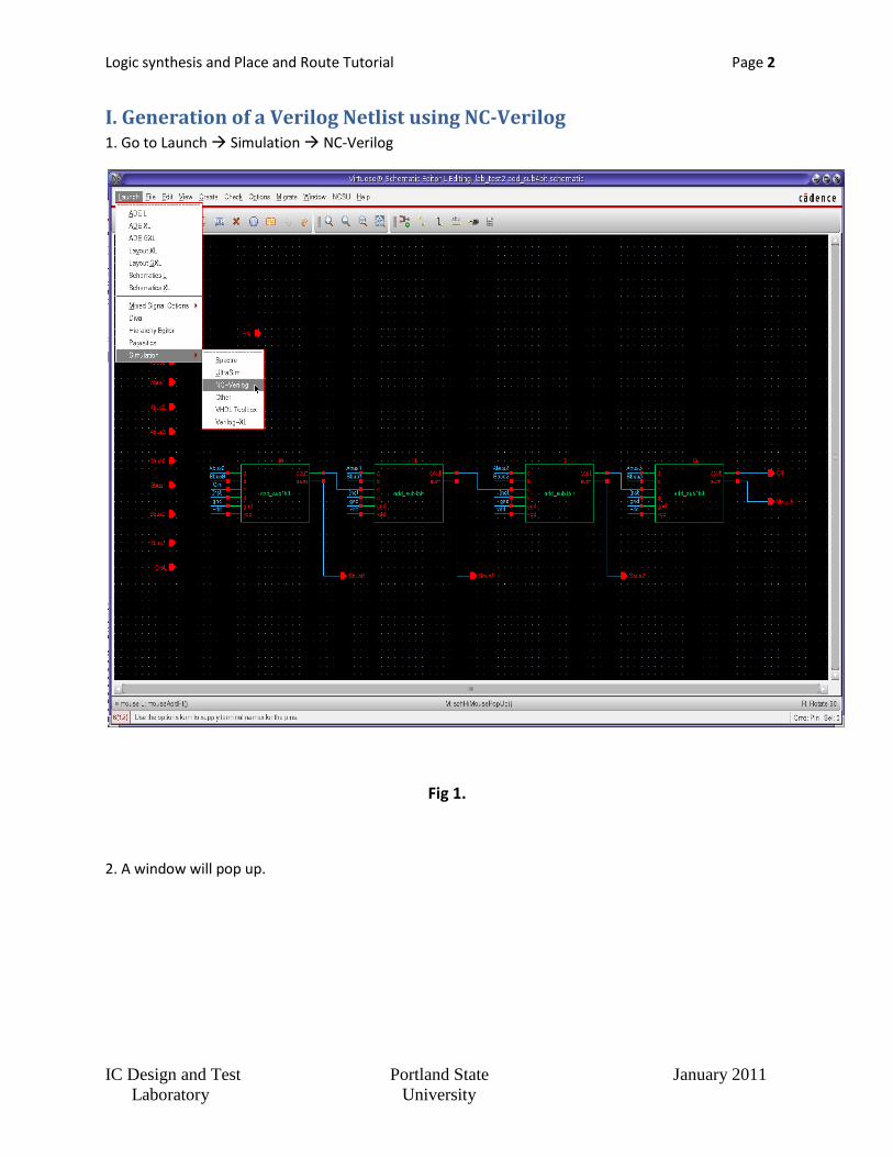
I. Generation of a Verilog Netlist using NC-Verilog 1. Go to Launch Simulation NC-Verilog
Fig 1.
2. A window will pop up.

Logic synthesis and Place and Route Tutorial Page 3
IC Design and Test Portland State January 2011
Laboratory University
Fig 2.
3. Go to Commands Initialize Design.
4. After Initializing the design, Go to Setup Netlist. A window will appear.
On the Netlisting Mode, click Entire design.
Click Netlist Explicitly
In the Global Power Nets change the value to vdd
In the Global Ground Nets change the value to gnd
5. The form window should like

Logic synthesis and Place and Route Tutorial Page 4
IC Design and Test Portland State January 2011
Laboratory University
Fig 3.
6. Click OK.
7. Go to Commands Generate Netlist
8. The status should be Netlist Succeeded.
9. Go to Results Netlist. A GUI-form will open up.
Fig. 4

Logic synthesis and Place and Route Tutorial Page 5
IC Design and Test Portland State January 2011
Laboratory University
10. Click on the library name which has your design. Click on any Cell name and click View. You will see
the verilog netlist of the design you made and also the netlist of instances that were used in your design.
So for example, If the top level design is a 4 bit adder, it will show you the netlist of a 4 bit adder with
four 1 bit full adders instantiated. Then there will be another netlist of a 1 bit full adder containing the
XOR, AND and OR cells instantiated.
11. When you open the netlist. Go to File Save as. Save all the netlist files in directory where you will
be invoking the PnR tool. The file name should be same as the module name. This is very important.
12. In the netlist containing the top-level design module, copy the contents of all the low level design
modules. So for example if the top-level HDL is 4 bit adder, copy the whole HDL definition of module
1bit adder in the top level HDL file.
13. Make sure you remove all the specify and endspecify staments
An example file will look like
module add_4bit ( Cout, Sbus0, Sbus1, Sbus2, Sbus3, Abus0, Abus1, Abus2, Abus3, Bbus0, Bbus1, Bbus2, Bbus3, Cin, gnd, vdd );
output Cout, Sbus0, Sbus1, Sbus2, Sbus3; input Abus0, Abus1, Abus2, Abus3, Bbus0, Bbus1, Bbus2, Bbus3, Cin, gnd, vdd; adder I3 ( .cout(Cout), .sum(Sbus3), .a(Abus3), .b(Bbus3), .c(net24), .gnd(gnd), .vdd(vdd)); adder I2 ( .cout(net24), .sum(Sbus2), .a(Abus2), .b(Bbus2),.c(net32), .gnd(gnd), .vdd(vdd)); adder I1 ( .cout(net32), .sum(Sbus1), .a(Abus1), .b(Bbus1),.c(net40), .gnd(gnd), .vdd(vdd)); adder I0 ( .cout(net40), .sum(Sbus0), .a(Abus0), .b(Bbus0),.c(Cin), .gnd(gnd), .vdd(vdd));
endmodule
module adder ( Cout, Sum, gnd, vdd, A, B, Cin );
output Cout, Sum; input A, B, Cin, gnd, vdd; XOR2X1 I4 ( .A(A), .B(B), .Y(net22), .gnd(gnd), .vdd(vdd)); XOR2X1 I5 ( .A(net22), .B(Cin), .Y(Sum), .gnd(gnd), .vdd(vdd)); AND2X1 I3 ( .A(A), .B(B), .Y(net27), .gnd(gnd), .vdd(vdd)); AND2X1 I2 ( .A(net22), .B(Cin), .Y(net32), .gnd(gnd), .vdd(vdd)); OR2X1 I6 ( .A(net32), .B(net27), .Y(Cout), .gnd(gnd), .vdd(vdd));
endmodule

Logic synthesis and Place and Route Tutorial Page 6
IC Design and Test Portland State January 2011
Laboratory University
II. Logic Synthesis and Place n Route Tutorial
This part is totally automated by a perl script PR.pl. The script removes gnd and vdd definitions from
your HDL input and gives it to synthesis tool. The RTL compiler takes logic gates from it’s own library
gscl45nm.v and builds your circuit and then optimizes it. Then the Encounter tool places the standard
cells between rows and routes the nets to produce an ASIC design.
1. Go to the directory where you have saved the HDL file and all the encounter files should be present.
2. In the command line,type
perl PR.pl Your_HDL_file_name.v
Again make sure the HDL file name is same as top level module name.
3. The script runs the cadence RTL compiler, synthesizes the design in logic gates and outputs a file
Your_HDL_file_name.vh
4. It will also output following files
i) rc.log --- This is the log file of the synthesis tool. The file shouldn’t have any errors or any
unexpected warnings. If there is an error, the whole flow will exit with an error.
A successful synthesis run should look like
Incremental optimization status =============================== Worst DRC Total Total Neg Max Operation Area Slack Cap Worst Path ------------------------------------------------------------------------------- init_delay 92 -140 11 Bbus0 --> Sbus3 init_drc 92 -140 11 Bbus0 --> Sbus3 init_area 92 -140 11 Bbus0 --> Sbus3 Done mapping add_sub4bit Synthesis succeeded. rc:/> rc:/> Tracing clock networks. Levelizing the circuit.
Applying wireload models.
Computing net loads.
Computing delays.
Computing arrivals and requireds.
rc:/> rc:/> rc:/> rc:/> rc:/> rc:/> rc:/>
rc:/> Synthesis Finished!
rc:/> Check timing.rep, area.rep, gate.rep and power.rep for synthesis results
Logic synthesis and Place and Route Tutorial Page 7
IC Design and Test Portland State January 2011
Laboratory University
ii) rc.cmd ---- this is the cmd file which is generated by RTL compiler. It contains all the internal
commands which are run in a typical logic synthesis flow.
iii) Files with extension .rep are generated which contain the timing and power information of the
design.
5. The output .vh file is given as input to Soc Encounter by the script itself and it starts running in
background.
6. The Encounter runs an encounter.tcl file. If you are interested you can open the file and see the
internal commands.
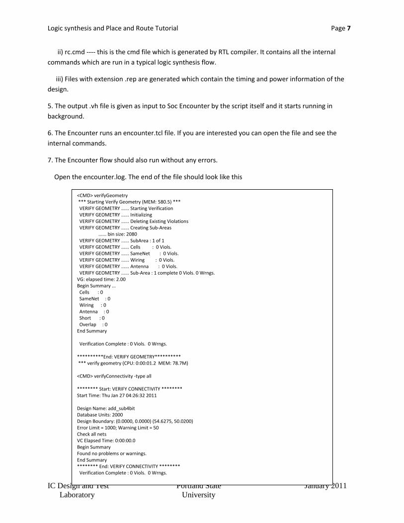
7. The Encounter flow should also run without any errors.
Open the encounter.log. The end of the file should look like this
<CMD> verifyGeometry *** Starting Verify Geometry (MEM: 580.5) *** VERIFY GEOMETRY ...... Starting Verification VERIFY GEOMETRY ...... Initializing VERIFY GEOMETRY ...... Deleting Existing Violations VERIFY GEOMETRY ...... Creating Sub-Areas ...... bin size: 2080 VERIFY GEOMETRY ...... SubArea : 1 of 1 VERIFY GEOMETRY ...... Cells : 0 Viols. VERIFY GEOMETRY ...... SameNet : 0 Viols. VERIFY GEOMETRY ...... Wiring : 0 Viols. VERIFY GEOMETRY ...... Antenna : 0 Viols. VERIFY GEOMETRY ...... Sub-Area : 1 complete 0 Viols. 0 Wrngs. VG: elapsed time: 2.00 Begin Summary ... Cells : 0 SameNet : 0 Wiring : 0 Antenna : 0 Short : 0 Overlap : 0 End Summary Verification Complete : 0 Viols. 0 Wrngs. **********End: VERIFY GEOMETRY********** *** verify geometry (CPU: 0:00:01.2 MEM: 78.7M) <CMD> verifyConnectivity -type all ******** Start: VERIFY CONNECTIVITY ******** Start Time: Thu Jan 27 04:26:32 2011 Design Name: add_sub4bit Database Units: 2000 Design Boundary: (0.0000, 0.0000) (54.6275, 50.0200) Error Limit = 1000; Warning Limit = 50 Check all nets VC Elapsed Time: 0:00:00.0 Begin Summary Found no problems or warnings. End Summary ******** End: VERIFY CONNECTIVITY ******** Verification Complete : 0 Viols. 0 Wrngs.

Logic synthesis and Place and Route Tutorial Page 8
IC Design and Test Portland State January 2011
Laboratory University
8. The Design Window should look like
Fig 5.
9. Go to the File Save DEF OK. The DEF file will be saved with your design name and will be your
final design output.
10. You can close the Encounter Window now. A HDL file final.v is also saved in the current directory.
This file is the HDL version of your design. We will use this file later for our LVS check.

Logic synthesis and Place and Route Tutorial Page 9
IC Design and Test Portland State January 2011
Laboratory University
III. Back Annotation of Design in Cadence Virtuoso
1. Open the ICFB window. Go to File Import DEF. A form will open up.
Give the path to your DEF file
Give the Target Library Name
Ref. Technology Libraries should be NCSU_TechLib_FreePDK45
From the Drop-Down Menu of “Technology From Library” Select the NCSU_Techlib_FreePDK45.
If you are not able to select anything from drop-down menu, click Use Template file and the
again click Use GUI Fields
Give the Target Cell Name
Give the Target View Name as layout
Give the Master Library List as freepdk45_cells
2. Click OK.
Fig 6.
Logic synthesis and Place and Route Tutorial Page 10
IC Design and Test Portland State January 2011
Laboratory University
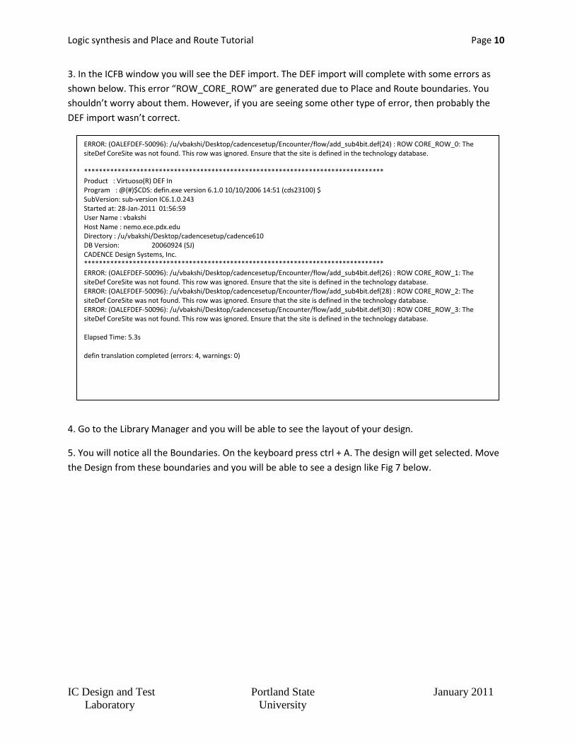
3. In the ICFB window you will see the DEF import. The DEF import will complete with some errors as
shown below. This error “ROW_CORE_ROW” are generated due to Place and Route boundaries. You
shouldn’t worry about them. However, if you are seeing some other type of error, then probably the
DEF import wasn’t correct.
4. Go to the Library Manager and you will be able to see the layout of your design.
5. You will notice all the Boundaries. On the keyboard press ctrl + A. The design will get selected. Move
the Design from these boundaries and you will be able to see a design like Fig 7 below.
ERROR: (OALEFDEF-50096): /u/vbakshi/Desktop/cadencesetup/Encounter/flow/add_sub4bit.def(24) : ROW CORE_ROW_0: The siteDef CoreSite was not found. This row was ignored. Ensure that the site is defined in the technology database. ******************************************************************************** Product : Virtuoso(R) DEF In Program : @(#)$CDS: defin.exe version 6.1.0 10/10/2006 14:51 (cds23100) $ SubVersion: sub-version IC6.1.0.243 Started at: 28-Jan-2011 01:56:59 User Name : vbakshi Host Name : nemo.ece.pdx.edu Directory : /u/vbakshi/Desktop/cadencesetup/cadence610 DB Version: 20060924 (SJ) CADENCE Design Systems, Inc. ******************************************************************************** ERROR: (OALEFDEF-50096): /u/vbakshi/Desktop/cadencesetup/Encounter/flow/add_sub4bit.def(26) : ROW CORE_ROW_1: The siteDef CoreSite was not found. This row was ignored. Ensure that the site is defined in the technology database. ERROR: (OALEFDEF-50096): /u/vbakshi/Desktop/cadencesetup/Encounter/flow/add_sub4bit.def(28) : ROW CORE_ROW_2: The siteDef CoreSite was not found. This row was ignored. Ensure that the site is defined in the technology database. ERROR: (OALEFDEF-50096): /u/vbakshi/Desktop/cadencesetup/Encounter/flow/add_sub4bit.def(30) : ROW CORE_ROW_3: The siteDef CoreSite was not found. This row was ignored. Ensure that the site is defined in the technology database. Elapsed Time: 5.3s defin translation completed (errors: 4, warnings: 0)

Logic synthesis and Place and Route Tutorial Page 11
IC Design and Test Portland State January 2011
Laboratory University
Fig 7.
6. Press shift + S. Click Add criteria and fill in the forms as shown below.
Logic synthesis and Place and Route Tutorial Page 12
IC Design and Test Portland State January 2011
Laboratory University
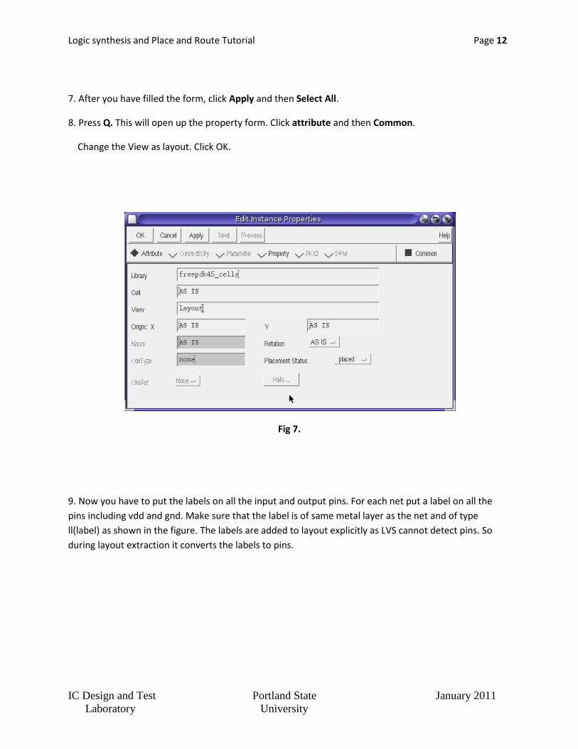
7. After you have filled the form, click Apply and then Select All.
8. Press Q. This will open up the property form. Click attribute and then Common.
Change the View as layout. Click OK.
Fig 7.
9. Now you have to put the labels on all the input and output pins. For each net put a label on all the
pins including vdd and gnd. Make sure that the label is of same metal layer as the net and of type
ll(label) as shown in the figure. The labels are added to layout explicitly as LVS cannot detect pins. So
during layout extraction it converts the labels to pins.

Logic synthesis and Place and Route Tutorial Page 13
IC Design and Test Portland State January 2011
Laboratory University
Fig 8.
10. Run DRC. It should come clean.
11. Open LVS form. Go to the Inputs section and then the netlist tab. Choose the format as verilog and
browse to get the final.v which you had saved in the PnR flow. Refer to figure below.

Logic synthesis and Place and Route Tutorial Page 14
IC Design and Test Portland State January 2011
Laboratory University
Fig 9.
12. The output of the LVS will come incorrect because of different number of nets and instances. That is
OK. However the results should not be ‘NOT COMPARED’. This means there was some error.
13. Go to Calibre Run Pex. A form will open up. Again go to Input Tab. Go to Netlist Tab. Again select
the verilog file final.v and format as VERILOG. It should look like the Fig 10.
14. Go to Output tab. Change the extraction to Transistor level, Extraction type as R + C and No
Inductance
15. Choose the format as SPECTRE and use names from Layout. Refer to Fig 10.
14. Click Run Pex.

Logic synthesis and Place and Route Tutorial Page 15
IC Design and Test Portland State January 2011
Laboratory University
Fig 10.
15. After some time, the PEX will complete with no errors. It will also show you the netlist. Make sure all
the input and output pins are declared including vdd and gnd.
16. The PEX outputs three files as the extracted netlist. These are:
{design name}.netlist
{design name}.pex
{design name}.pxi
The starting part of .netlist should look like below. Make sure all the input and output pins are
showing in the netlist. This netlist contains all the extracted transistors, resistance and capacitances.

Logic synthesis and Place and Route Tutorial Page 16
IC Design and Test Portland State January 2011
Laboratory University
// File: add_sub4bit.pex.netlist // Created: Fri Jan 28 04:06:36 2011 // Program "Calibre xRC" // Version "v2007.1_24.22" // include "add_sub4bit.pex.netlist.pex" subckt ADD_SUB4BIT ( C4 SBUS0 SBUS1 SBUS2 SBUS3 ABUS0 ABUS1 ABUS2 ABUS3 BBUS0 \ BBUS1 BBUS2 BBUS3 CIN INST VDD GND ) // // SBUS0 SBUS0 // SBUS3 SBUS3 // ABUS0 ABUS0 // ABUS1 ABUS1 // BBUS0 BBUS0 // BBUS1 BBUS1 // ABUS2 ABUS2 // ABUS3 ABUS3 // BBUS2 BBUS2 // BBUS3 BBUS3 // C4 C4 // CIN CIN // SBUS1 SBUS1 // SBUS2 SBUS2 // GND GND // VDD VDD

Logic synthesis and Place and Route Tutorial Page 17
IC Design and Test Portland State January 2011
Laboratory University
IV. Simulating an PEX extracted netlist
Couple of hacks to done before we are ready for simulating our extracted netlist.
1. On the command line,
> mkdir spectre.run1/
2. Copy your all three extracted netlist files in this directory.
3. Rename the .netlist file as netlist. On the command line write
> mv *.netlist netlist
4. In the spectre.run1/ directory type on the command line
> cp ./netlist ./input.scs
This input.scs file will be input to your ocean script. Open input.scs in gedit. This will be your new
input.scs
When you simulated your schematic, a directory called simulation is formed in the current running
directory. The directory contains an input.scs file.
An example of the path will be like:
/u/username/Desktop/cadence610/simulation/add_sub4bit_test/spectre/schematic/netlist
Go to this directory and open the input.scs file in gedit. Remember this is your old input.scs file in which
you simulated your schematic. Now you have two input.scs file open, one is the old version (the one
which simulated your schematic) and another will be your new version.
Do not get confused by two input.scs files
In Old input.scs, you will see the starting lines something like below:
simulator lang=spectre global 0 include "/u/vbakshi/Desktop/cadencesetup/cadence610/50nmodels.m" // Library name: freepdk45_cells // Cell name: XOR2X1 // View name: schematic //

Logic synthesis and Place and Route Tutorial Page 18
IC Design and Test Portland State January 2011
Laboratory University
5. Copy these first three lines at the top of your new input.scs file.
6. Again at the end of your old input.scs file after the “End of subcircuit Definition”, you will notice all
instantiation of your circuit, voltage sources and ground definitions will be there. An example will be
7. Copy all the lines after “End of subcircuit Definition” in your new input.scs file.
8. Close the old input.scs file
9. In your new input.scs file, notice that the subcircuit has been instantiated like
subckt ADD_SUB4BIT ( C4 SBUS0 SBUS1 SBUS2 SBUS3 ABUS0 ABUS1 ABUS2 ABUS3 BBUS0 \
BBUS1 BBUS2 BBUS3 CIN INST VDD GND )
Then at end of subcircuit definitions, you will notice the instantiation of your subcircuit
I0 (net29 net29 net27 net27 net25 net25 net23 net23 C4 0 0 Sbus0 Sbus1 \
Sbus2 Sbus3 0 net31) add_sub4bit
// End of subcircuit definition. // Library name: lab_test2 // Cell name: add_sub4bit_test // View name: schematic I0 (net29 net29 net27 net27 net25 net25 net23 net23 C4 0 0 Sbus0 Sbus1 \ Sbus2 Sbus3 0 net31) add_sub4bit V6 (net23 0) vsource type=pwl wave=[ 0 1.2 18n 1.2 18.2n 0 30n 0 30.2n 1.2 \ 45n 1.2 ] V5 (net25 0) vsource type=pwl wave=[ 0 0 12n 0 12.2n 1.2 25n 1.2 25.2n 0 \ 35n 0 ] V1 (net27 0) vsource type=pwl wave=[ 0 1.2 18n 1.2 18.2n 0 30n 0 30.2n 1.2 \ 45n 1.2 ] V0 (net29 0) vsource type=pwl wave=[ 0 0 12n 0 12.2n 1.2 25n 1.2 25.2n 0 \ 35n 0 ] V4 (net31 0) vsource type=dc dc=1.2 simulatorOptions options reltol=1e-3 vabstol=1e-6 iabstol=1e-12 temp=27 \ tnom=27 scalem=1.0 scale=1.0 gmin=1e-12 rforce=1 maxnotes=5 maxwarns=5 \ digits=5 cols=80 pivrel=1e-3 sensfile="../psf/sens.output" \ checklimitdest=psf tran tran stop=100n write="spectre.ic" writefinal="spectre.fc" \ annotate=status maxiters=5 finalTimeOP info what=oppoint where=rawfile modelParameter info what=models where=rawfile element info what=inst where=rawfile outputParameter info what=output where=rawfile designParamVals info what=parameters where=rawfile primitives info what=primitives where=rawfile subckts info what=subckts where=rawfile saveOptions options save=allpub

Logic synthesis and Place and Route Tutorial Page 19
IC Design and Test Portland State January 2011
Laboratory University
These nets should be in the same order as the subcircuit definition. You will notice that order is not
correct above. Edit it to make connections in proper order. An example of proper order will be:
I0 (C4 Sbus0 Sbus1 Sbus2 Sbus3 net29 net29 net27 net27 net25 net25 net23 net23 \
0 0 net31 0) ADD_SUB4BIT.
10. One final hack
Open the .pex netlist file and at the top of the file include this line
simulator lang=spectre
11. Now you are ready for some simulation!!!
Download the Ocean Script from the website. Edit the Ocean Script to give proper paths. The input file
will be your “spectre.run1/netlist”
Run the Ocean script.

Logic synthesis and Place and Route Tutorial Page 20
IC Design and Test Portland State January 2011
Laboratory University
V. Direct Place and Route tutorial
1. Go to the Encounter/flow Directory.
2. Before coming to this stage, make sure you have run a synthesis and place and route design flow. In
the flow directory you see there will two files HDL_name.v and HDL_name.vh
HDL_name.v is your verilog file created by NC-verilog from your schematic. This is your un-optimized
design.
HDL_name.vh is the optimized design produced by logic synthesis and given as input to Encounter which
places and routes the standard cells.
3. Delete the .vh extension file. On the command line
> rm HDL_name.vh
4. Rename the original verilog file as .vh file. On the command line write
> mv HDL_name.v HDL_name.vh
5. This file will become input to your encounter tool and it will place and route your original design. On
the command line write
> encounter –init encounter.tcl
You have to use the new encounter.tcl for this.
6. The rest of the flow is same. After the encounter finishes, save the DEF file and import into cadence
virtuoso. Extract the netlist with parasitics and simulate it.


![GCC internals intro y optimizationesnicolasw/Docencia/CP/gcc_int_intro.pdf · Optimizaciones Back-end Backend: – RTL tree + RTL language + RTL Engine + RTL Compiler [Middle-End]](https://img.pdfslide.net/doc/110x75/5f066be67e708231d417e97b/gcc-internals-intro-y-optimizationes-nicolaswdocenciacpgccintintropdf-optimizaciones.jpg)