Embed Size (px)
Citation preview

Data Sheet
www.rohm.com© 2014 ROHM Co., Ltd. All rights reserved.
R6047ENZ1 Nch 600V 47A Power MOSFET
Reverse diode dv/dt dv/dt *4 15 V/ns
Junction temperature Tj 150 °C
Range of storage temperature Tstg -55 to +150 °C
Avalanche current, repetitive IAR 9.3 A
Power dissipation (Tc = 25°C) PD 120 W
Avalanche energy, single pulse EAS *3 1135 mJ
Avalanche energy, repetitive EAR *3 1.72 mJ
Pulsed drain current ID,pulse *2
141 A
Gate - Source voltage VGSS 20 V
Continuous drain currentTc = 25°C ID
*147 A
Tc = 100°C ID *1
25.5 A
Drain - Source voltage VDSS 600 V
Taping code C9
Marking R6047ENZ1
lAbsolute maximum ratings (Ta = 25°C)
Parameter Symbol Value Unit
6) Pb-free lead plating ; RoHS compliantlPackaging specifications
Type
Packaging Tube
Reel size (mm) -
lApplication Tape width (mm) -
Switching Power Supply Basic ordering unit (pcs) 450
lFeatures lInner circuit
1) Low on-resistance.
2) Fast switching speed.
3) Gate-source voltage (VGSS) guaranteed to be 20V.
4) Drive circuits can be simple.
5) Parallel use is easy.
lOutline
VDSS 600V TO-247
RDS(on) (Max.) 0.072W
ID 47APD 120W (1)
(3) (2)
(1) Gate (2) Drain (3) Source
*1 BODY DIODE
1/12 2014.03 - Rev.B

www.rohm.com© 2014 ROHM Co., Ltd. All rights reserved.
Data SheetR6047ENZ1
WGate input resistance RG f = 1MHz, open drain - 0.8 -
0.066 0.072
Tj = 125°C - 0.140 -
V
Static drain - sourceon - state resistance RDS(on)
*5
VGS = 10V, ID = 25.8A
WTj = 25°C -
Gate threshold voltage VGS (th) VDS = 10V, ID = 1mA 2 - 4
Gate - Source leakage current IGSS VGS = 20V, VDS = 0V - - 100 nA
mATj = 25°C - 0.1 100
Tj = 125°C - - 1000
Zero gate voltagedrain current
IDSS
VDS = 600V, VGS = 0V
VDrain - Source breakdownvoltage
V(BR)DSS VGS = 0V, ID = 1mA 600 - -
lElectrical characteristics (Ta = 25°C)
Parameter Symbol ConditionsValues
UnitMin. Typ. Max.
Soldering temperature, wavesoldering for 10s Tsold - - 265 °C
Thermal resistance, junction - ambient RthJA - - 30 °C/W
Thermal resistance, junction - case RthJC - - 1.04 °C/W
lThermal resistance
Parameter SymbolValues
UnitMin. Typ. Max.
Drain - Source voltage slope dv/dtVDS = 480V
50 V/nsTj = 125°C
lAbsolute maximum ratings
Parameter Symbol Conditions Values Unit
2/12 2014.03 - Rev.B

www.rohm.com© 2014 ROHM Co., Ltd. All rights reserved.
Data SheetR6047ENZ1
*1 Limited only by maximum temperature allowed.
*2 PW 10ms, Duty cycle 1%
*3 ID = 9.3A, VDD = 50V
*4 Reference measurement circuits Fig.5-1.
*5 Pulsed
Gate plateau voltage V(plateau) VDD ⋍ 300V, ID = 47A - 6.2 -
nCGate - Source charge Qgs *5 ID = 47A - 20 -
Gate - Drain charge Qgd *5 VGS = 10V
Total gate charge Qg *5 VDD ⋍ 300V
UnitMin. Typ. Max.
V
- 80 -
-
- 145 -
lGate Charge characteristics (Ta = 25°C)
Parameter Symbol ConditionsValues
nsRise time tr
*5 ID = 23.5A - 100 -
Turn - off delay time td(off) *5 RL = 12.7W
Turn - on delay time td(on) *5 VDD ⋍ 300V, VGS = 10V - 50 -
- 260 -
Fall time tf *5 RG = 10W - 100
320 -
pFEffective output capacitance,time related
Co(tr) - 710 -
Effective output capacitance,energy related
Co(er)
VGS = 0VVDS = 0V to 480V
- 140 -
S
Input capacitance Ciss VGS = 0V - 3850 -
pFOutput capacitance Coss
Transconductance gfs *5 VDS = 10V, ID = 23.5A 13 26 -
VDS = 25V - 2950 -
Reverse transfer capacitance Crss f = 1MHz -
lElectrical characteristics (Ta = 25°C)
Parameter Symbol ConditionsValues
UnitMin. Typ. Max.
3/12 2014.03 - Rev.B

www.rohm.com© 2014 ROHM Co., Ltd. All rights reserved.
Data SheetR6047ENZ1
Ws/KRth2 0.428 Cth2 0.539
Rth3 0.250 Cth3 16.7
Rth1 0.111
K/W
Cth1 0.0246
lTypical Transient Thermal Characteristics
Symbol Value Unit Symbol Value Unit
- 18 - mC
Peak reverse recovery current Irrm *5 - 45 - A
V
Reverse recovery time trr *5
IS = 47Adi/dt = 100A/ms
- 850 - ns
Reverse recovery charge Qrr *5
Forward voltage VSD *5 VGS = 0V, IS = 47A - - 1.5
A
Inverse diode direct current,pulsed ISM *2 - - 141 A
Inverse diode continuous,forward current IS *1
Tc = 25°C
- - 47
lBody diode electrical characteristics (Source-Drain) (Ta = 25°C)
Parameter Symbol ConditionsValues
UnitMin. Typ. Max.
4/12 2014.03 - Rev.B
www.rohm.com© 2014 ROHM Co., Ltd. All rights reserved.
Data SheetR6047ENZ1
lElectrical characteristic curves
0
20
40
60
80
100
120
0 50 100 150 2000.0001
0.001
0.01
0.1
1
10
100
1000
0.0001 0.001 0.01 0.1 1 10 100 1000
Ta = 25ºC Single Pulse Rth(ch-a)(t) = r(t)×Rth(ch-a) Rth(ch-a) = 30ºC/W
top D = 1 D = 0.5 D = 0.1 D = 0.05 D = 0.01 D = Single
0
20
40
60
80
100
120
0 25 50 75 100 125 150 175
Fig.1 Power Dissipation Derating Curve
Pow
er D
issi
patio
n :
PD/P
D m
ax. [
%]
Junction Temperature : Tj [°C]
Fig.2 Normalized Transient Thermal Resistance vs. Pulse Width
Nor
mal
ized
Tra
nsie
nt T
herm
al R
esis
tanc
e : r
(t)
Pulse Width : PW [s]
Fig.3 Avalanche Energy Derating Curve vs Junction Temperature
Ava
lanc
he E
nerg
y : E
AS /
E AS
max
. [%
]
Junction Temperature : Tj [ºC]
5/12 2014.03 - Rev.B
www.rohm.com© 2014 ROHM Co., Ltd. All rights reserved.
Data SheetR6047ENZ1
lElectrical characteristic curves
0
5
10
15
20
25
30
35
40
45
0 1 2 3 4 5 6 7 8 9 10
Ta=150ºC Pulsed
VGS= 10.0V
VGS= 4.5V
VGS= 8.0V VGS= 7.0V
VGS= 6.5V
VGS= 5.5V
VGS= 5.0V
VGS= 6.0V
0
5
10
15
20
25
30
35
40
45
0 10 20 30 40 50
Ta=150ºC Pulsed
VGS= 10.0V
VGS= 4.5V
VGS= 8.0V VGS= 7.0V VGS= 6.5V
VGS= 6.0V
VGS= 5.5V
VGS= 5.0V
0
5
10
15
20
25
30
35
40
45
0 1 2 3 4 5
Ta=25ºC Pulsed
VGS= 10.0V
VGS= 4.5V
VGS= 8.0V VGS= 7.0V
VGS= 6.5V VGS= 6.0V
VGS= 5.0V
0
5
10
15
20
25
30
35
40
45
0 10 20 30 40 50
Ta=25ºC Pulsed
VGS= 10.0V
VGS= 4.5V
VGS= 8.0V VGS= 7.0V VGS= 6.5V VGS= 6.0V
VGS= 5.0V
Fig.4 Typical Output Characteristics(I) Fig.5 Typical Output Characteristics(II)
Fig.6 Tj = 150°C Typical Output Characteristics(I)
Fig.7 Tj = 150°C Typical Output Characteristics(II)
Drain - Source Voltage : VDS [V] Drain - Source Voltage : VDS [V]
Dra
in C
urre
nt :
I D [A
]
Dra
in C
urre
nt :
I D [A
]
Dra
in C
urre
nt :
I D [A
]
Drain - Source Voltage : VDS [V]
Dra
in C
urre
nt :
I D [A
]
Drain - Source Voltage : VDS [V]
6/12 2014.03 - Rev.B

www.rohm.com© 2014 ROHM Co., Ltd. All rights reserved.
Data SheetR6047ENZ1
lElectrical characteristic curves
500
550
600
650
700
750
800
850
900
-50 -25 0 25 50 75 100 125 1500.001
0.01
0.1
1
10
100
0 2 4 6 8 10
Ta=125ºC Ta=75ºC Ta=25ºC Ta= -25ºC
VDS= 10V
2.0
2.5
3.0
3.5
4.0
-50 -25 0 25 50 75 100 125 150
VDS= 10V ID= 1mA
0.01
0.1
1
10
100
0.01 0.1 1 10 100
Ta= -25ºC Ta=25ºC Ta=75ºC Ta=125ºC
VDS= 10V
Fig.9 Typical Transfer Characteristics Fig.8 Breakdown Voltage vs. Junction Temperature
Dra
in -
Sour
ce B
reak
dow
n Vo
ltage
: V
(BR
)DSS
[V]
Dra
in C
urre
nt :
I D [A
]
Fig.10 Gate Threshold Voltage vs. Junction Temperature
Gat
e Th
resh
old
Volta
ge :
VG
S(th
) [V]
Junction Temperature : Tj [°C]
Fig.11 Transconductance vs. Drain Current
Tran
scon
duct
ance
: g f
s [S]
Drain Current : ID [A]
Junction Temperature : Tj [°C] Gate - Source Voltage : VGS [V]
7/12 2014.03 - Rev.B

www.rohm.com© 2014 ROHM Co., Ltd. All rights reserved.
Data SheetR6047ENZ1
lElectrical characteristic curves
0
50
100
150
200
0 5 10 15 20
ID = 47A
ID = 25.8A
Ta=25ºC
1
10
100
1000
10000
0.01 0.1 1 10 100
Ta=25ºC
VGS= 10V
0
20
40
60
80
100
120
140
160
180
200
-50 -25 0 25 50 75 100 125 150
VGS= 10V ID = 25.8A
1
10
100
1000
10000
0.01 0.1 1 10 100
Ta=125ºC Ta=75ºC Ta=25ºC Ta= -25ºC
VGS= 10V
Fig.12 Static Drain - Source On - State Resistance vs. Gate Source Voltage
Stat
ic D
rain
- So
urce
On-
Stat
e R
esis
tanc
e
: RD
S(on
) [m
W]
Gate - Source Voltage : VGS [V]
Fig.13 Static Drain - Source On - State Resistance vs. Junction Temperature
Stat
ic D
rain
- So
urce
On-
Stat
e R
esis
tanc
e
: RD
S(on
) [m
W]
Junction Temperature : Tj [ºC]
Fig.14 Static Drain - Source On - State Resistance vs. Drain Current
Stat
ic D
rain
- So
urce
On-
Stat
e R
esis
tanc
e
: RD
S(on
) [m
W]
Drain Current : ID [A]
Fig.15 Static Drain - Source On - State Resistance vs. Drain Current
Stat
ic D
rain
- So
urce
On-
Stat
e R
esis
tanc
e
: RD
S(on
) [m
W]
Drain Current : ID [A]
8/12 2014.03 - Rev.B

www.rohm.com© 2014 ROHM Co., Ltd. All rights reserved.
Data SheetR6047ENZ1
lElectrical characteristic curves
0
5
10
15
20
25
30
0 200 400 600
Ta=25ºC
1
10
100
1000
10000
100000
0.01 0.1 1 10 100 1000
Coss
Crss
Ciss
Ta=25ºC f = 1MHz VGS = 0V
1
10
100
1000
10000
100000
0.01 0.1 1 10 100
tr
tf
td(on)
td(off)
Ta = 25ºC VDD = 300V VGS = 10V RG= 10W
0
2
4
6
8
10
12
14
16
18
20
0 50 100 150 200 250 300
Ta = 25ºC VDD= 300V ID= 47A
Fig.16 Typical Capacitance vs. Drain - Source Voltage
Cap
acita
nce
: C [p
F]
Drain - Source Voltage : VDS [V]
Fig.18 Switching Characteristics
Switc
hing
Tim
e : t
[ns]
Drain Current : ID [A]
Fig.19 Dynamic Input Characteristics
Total Gate Charge : Qg [nC]
Gat
e - S
ourc
e Vo
ltage
: V
GS
[V]
Cos
s St
ored
Ene
rgy
: EO
SS [u
J]
Fig.17 Coss Stored Energy
Drain - Source Voltage : VDS [V]
9/12 2014.03 - Rev.B

www.rohm.com© 2014 ROHM Co., Ltd. All rights reserved.
Data SheetR6047ENZ1
lElectrical characteristic curves
Inve
rse
Dio
de F
orw
ard
Cur
rent
: I S
[A]
10
100
1000
10000
0.1 1 10 100
Ta=25ºC di / dt = 100A / ms VGS = 0V
0.01
0.1
1
10
100
0.0 0.5 1.0 1.5
Ta=125ºC Ta=75ºC Ta=25ºC Ta= -25ºC
VGS=0V
Fig.20 Inverse Diode Forward Current vs. Source - Drain Voltage
Source - Drain Voltage : VSD [V]
Fig.21 Reverse Recovery Time vs.Inverse Diode Forward Current
Rev
erse
Rec
over
y Ti
me
: trr [n
s]
Inverse Diode Forward Current : IS [A]
10/12 2014.03 - Rev.B

www.rohm.com© 2014 ROHM Co., Ltd. All rights reserved.
Data SheetR6047ENZ1
lMeasurement circuits
Fig.1-1 Switching Time Measurement Circuit Fig.1-2 Switching Waveforms
Fig.2-1 Gate Charge Measurement Circuit Fig.2-2 Gate Charge Waveform
Fig.3-1 Avalanche Measurement Circuit Fig.3-2 Avalanche Waveform
Fig.4-1 dv/dt Measurement Circuit Fig.4-2 dv/dt Waveform
Fig.5-1 di/dt Measurement Circuit Fig.5-2 di/dt Waveform
11/12 2014.03 - Rev.B
www.rohm.com© 2014 ROHM Co., Ltd. All rights reserved.
Data SheetR6047ENZ1
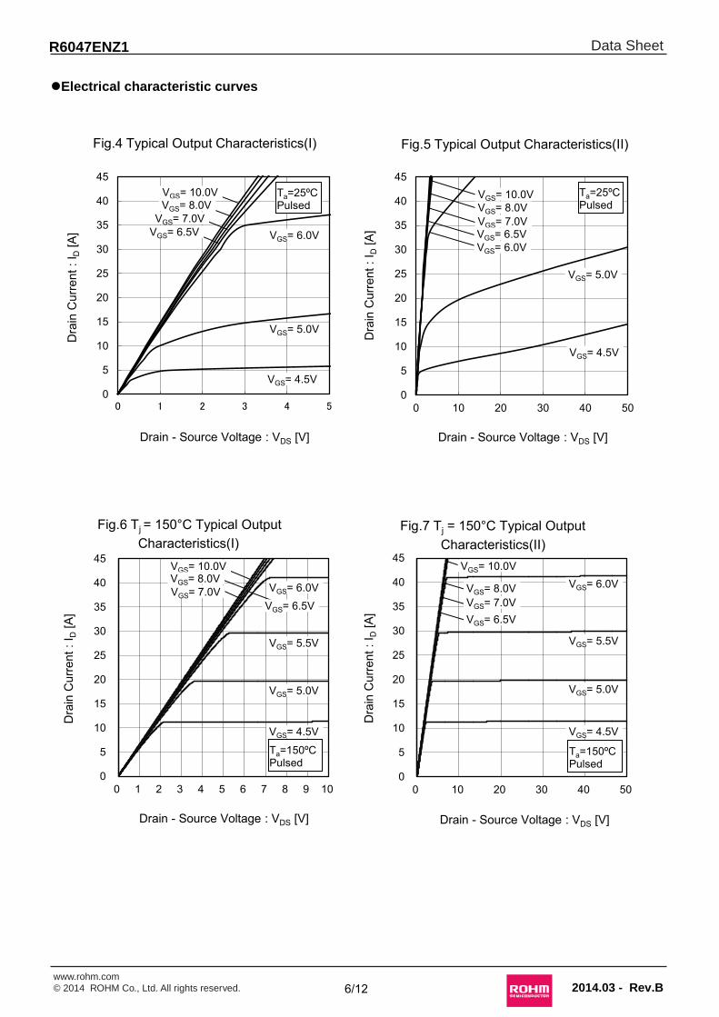
lDimensions (Unit : mm)
Dimension in mm / inches
TO-247
MIN MAX MIN MAX
A 4.83 5.21 0.190 0.205
A1 2.29 2.54 0.090 0.100
A2 1.91 2.16 0.075 0.085
b 1.14 1.40 0.045 0.055
b1 1.91 2.20 0.075 0.087
b2 2.92 3.20 0.115 0.126
c 0.61 0.80 0.024 0.031
D 20.80 21.34 0.819 0.840
D1 17.43 17.83 0.686 0.702
E 15.75 16.13 0.620 0.635
e
N
L 19.81 20.57 0.780 0.810
L1 3.81 4.32 0.150 0.170
Φ P 3.55 3.65 0.140 0.144
Q 5.59 6.20 0.220 0.244
S
DIMMILIMETERS INCHES
5.45 0.215
3.00 3.000
6.15 0.240
12/12 2014.03 - Rev.B

R1102Awww.rohm.com© 2014 ROHM Co., Ltd. All rights reserved.
Notice
ROHM Customer Support System http://www.rohm.com/contact/
Thank you for your accessing to ROHM product informations. More detail product informations and catalogs are available, please contact us.
N o t e s The information contained herein is subject to change without notice.
Before you use our Products, please contact our sales representative and verify the latest specifica-tions :
Although ROHM is continuously working to improve product reliability and quality, semicon-ductors can break down and malfunction due to various factors.Therefore, in order to prevent personal injury or fire arising from failure, please take safety measures such as complying with the derating characteristics, implementing redundant and fire prevention designs, and utilizing backups and fail-safe procedures. ROHM shall have no responsibility for any damages arising out of the use of our Poducts beyond the rating specified by ROHM.
Examples of application circuits, circuit constants and any other information contained herein are provided only to illustrate the standard usage and operations of the Products. The peripheral conditions must be taken into account when designing circuits for mass production.
The technical information specified herein is intended only to show the typical functions of and examples of application circuits for the Products. ROHM does not grant you, explicitly or implicitly, any license to use or exercise intellectual property or other rights held by ROHM or any other parties. ROHM shall have no responsibility whatsoever for any dispute arising out of the use of such technical information.
The Products are intended for use in general electronic equipment (i.e. AV/OA devices, communi-cation, consumer systems, gaming/entertainment sets) as well as the applications indicated in this document.
The Products specified in this document are not designed to be radiation tolerant.
For use of our Products in applications requiring a high degree of reliability (as exemplified below), please contact and consult with a ROHM representative : transportation equipment (i.e. cars, ships, trains), primary communication equipment, traffic lights, fire/crime prevention, safety equipment, medical systems, servers, solar cells, and power transmission systems.
Do not use our Products in applications requiring extremely high reliability, such as aerospace equipment, nuclear power control systems, and submarine repeaters.
ROHM shall have no responsibility for any damages or injury arising from non-compliance with the recommended usage conditions and specifications contained herein.
ROHM has used reasonable care to ensur the accuracy of the information contained in this document. However, ROHM does not warrants that such information is error-free, and ROHM shall have no responsibility for any damages arising from any inaccuracy or misprint of such information.
Please use the Products in accordance with any applicable environmental laws and regulations, such as the RoHS Directive. For more details, including RoHS compatibility, please contact a ROHM sales office. ROHM shall have no responsibility for any damages or losses resulting non-compliance with any applicable laws or regulations.
When providing our Products and technologies contained in this document to other countries, you must abide by the procedures and provisions stipulated in all applicable export laws and regulations, including without limitation the US Export Administration Regulations and the Foreign Exchange and Foreign Trade Act.
This document, in part or in whole, may not be reprinted or reproduced without prior consent of ROHM.
1)
2)
3)
4)
5)
6)
7)
8)
9)
10)
11)
12)
13)
14)

Datasheet
Part Number R6047ENZ1Package TO-247Unit Quantity 450Minimum Package Quantity 450Packing Type BulkConstitution Materials List inquiryRoHS Yes
R6047ENZ1 - Web PageDistribution Inventory


![ALUMINUM ELECTROLYTIC CAPACITORS · 2017. 9. 23. · 66 SZ [ For Ultra Low ESR ] 2,000hrs. at 105qC 68 SQ [ High Temperature for +125ºC ] 1,000hrs. at 125qC 70 SV [ For adapter and](https://img.pdfslide.net/doc/110x75/60df3d78fe788b42d145f231/aluminum-electrolytic-capacitors-2017-9-23-66-sz-for-ultra-low-esr-2000hrs.jpg)