Embed Size (px)
Citation preview
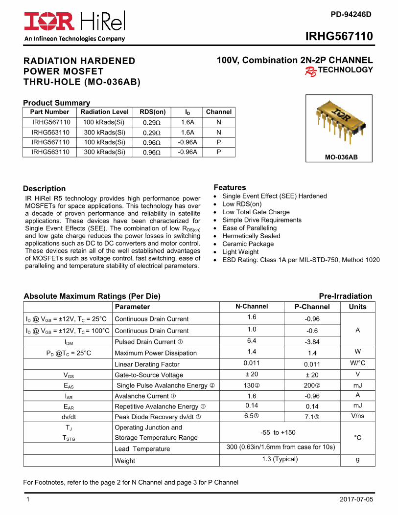
Features Single Event Effect (SEE) Hardened Low RDS(on) Low Total Gate Charge Simple Drive Requirements Ease of Paralleling Hermetically Sealed Ceramic Package Light Weight ESD Rating: Class 1A per MIL-STD-750, Method 1020
Absolute Maximum Ratings (Per Die) Pre-Irradiation Parameter N-Channel P-Channel Units
ID @ VGS = ±12V, TC = 25°C Continuous Drain Current 1.6 -0.96
A ID @ VGS = ±12V, TC = 100°C Continuous Drain Current 1.0 -0.6
IDM Pulsed Drain Current 6.4 -3.84
PD @TC = 25°C Maximum Power Dissipation 1.4 1.4 W
Linear Derating Factor 0.011 0.011 W/°C
VGS Gate-to-Source Voltage ± 20 ± 20 V
EAS Single Pulse Avalanche Energy 130 200 mJ
IAR Avalanche Current 1.6 -0.96 A
EAR Repetitive Avalanche Energy 0.14 0.14 mJ
dv/dt Peak Diode Recovery dv/dt 6.5 7.1 V/ns
TJ Operating Junction and -55 to +150
TSTG Storage Temperature Range
Lead Temperature 300 (0.63in/1.6mm from case for 10s)
Weight 1.3 (Typical)
°C
g
MO-036AB
IRHG567110
1 2017-07-05
Product Summary Part Number Radiation Level RDS(on) ID
IRHG567110 100 kRads(Si) 0.29 1.6A
IRHG563110 300 kRads(Si) 0.29 1.6A
IRHG567110 100 kRads(Si) 0.96 -0.96A
IRHG563110 300 kRads(Si) 0.96 -0.96A
Channel
N
N
P
P
RADIATION HARDENED POWER MOSFET THRU-HOLE (MO-036AB)
PD-94246D
Description
For Footnotes, refer to the page 2 for N Channel and page 3 for P Channel
RR 5
100V, Combination 2N-2P CHANNEL TECHNOLOGY
IR HiRel R5 technology provides high performance power MOSFETs for space applications. This technology has over a decade of proven performance and reliability in satellite applications. These devices have been characterized for Single Event Effects (SEE). The combination of low RDS(on)
and low gate charge reduces the power losses in switching applications such as DC to DC converters and motor control. These devices retain all of the well established advantages of MOSFETs such as voltage control, fast switching, ease of paralleling and temperature stability of electrical parameters.

2 2017-07-05
IRHG567110
Pre-Irradiation
Electrical Characteristics for Each N-Channel Device @ Tj = 25°C (Unless Otherwise Specified)
Parameter Min. Typ. Max. Units Test Conditions BVDSS Drain-to-Source Breakdown Voltage 100 ––– ––– V VGS = 0V, ID = 1.0mA BVDSS/TJ Breakdown Voltage Temp. Coefficient ––– 0.14 ––– V/°C Reference to 25°C, ID = 1.0mA
RDS(on) Static Drain-to-Source On-State
––– ––– 0.29 Resistance
VGS(th) Gate Threshold Voltage 2.0 ––– 4.0 V VDS = VGS, ID = 1.0mA Gfs Forward Transconductance 1.0 ––– ––– S VDS = 15V, ID = 1.0A IDSS Zero Gate Voltage Drain Current
––– ––– 10 µA
VDS = 80V, VGS = 0V ––– ––– 25 VDS = 80V,VGS = 0V,TJ =125°C
IGSS Gate-to-Source Leakage Forward ––– ––– 100 nA
VGS = 20V Gate-to-Source Leakage Reverse ––– ––– -100 VGS = -20V
QG Total Gate Charge ––– ––– 17
nC
ID = 1.6A
QGS Gate-to-Source Charge ––– ––– 4.4 VDS = 50V
QGD Gate-to-Drain (‘Miller’) Charge ––– ––– 3.9 VGS = 12V td(on) Turn-On Delay Time ––– ––– 21
ns
VDD = 50V tr Rise Time ––– ––– 16 ID = 1.6A td(off) Turn-Off Delay Time ––– ––– 50 RG = 7.5 tf Fall Time ––– ––– 15 VGS = 12V
Ls +LD Total Inductance ––– 10 ––– nH
Measured from Drain lead (6mm / 0.25 in from package) to Source lead (6mm/ 0.25 in from package) with Source wire internally bonded from Source pin to Drain pad
Ciss Input Capacitance ––– 370 ––– pF
VGS = 0V Coss Output Capacitance ––– 110 ––– VDS = 25V Crss Reverse Transfer Capacitance ––– 3.4 ––– ƒ = 1.0MHz
VGS = 12V, ID = 1.0A
Source-Drain Diode Ratings and Characteristics for Each N-Channel Device Parameter Min. Typ. Max. Units Test Conditions
IS Continuous Source Current (Body Diode) ––– ––– 1.6
ISM Pulsed Source Current (Body Diode) ––– ––– 6.4
VSD Diode Forward Voltage ––– ––– 1.2 V TJ = 25°C,IS = 1.6A, VGS = 0V
trr Reverse Recovery Time ––– ––– 110 ns TJ=25°C, IF = 1.6A, VDD ≤ 25V
Qrr Reverse Recovery Charge ––– ––– 380 nC di/dt = 100A/µs
ton Forward Turn-On Time Intrinsic turn-on time is negligible (turn-on is dominated by LS+LD)
A
* Values established by Thermal Modeling
Footnotes:
Repetitive Rating; Pulse width limited by maximum junction temperature.
VDD = 25V, starting TJ = 25°C, L =100mH, Peak IL = 1.6A, VGS = 12V
ISD 1.6A, di/dt 340A/µs, VDD 100V, TJ 150°C
Pulse width 300 µs; Duty Cycle 2%
Total Dose Irradiation with VGS Bias. 12 volt VGS applied and VDS = 0 during irradiation per MIL-STD-750, Method 1019, condition A.
Total Dose Irradiation with VDS Bias. 80volt VDS applied and VGS = 0 during irradiation per MlL-STD-750, Method 1019, condition A.
Thermal Resistance for Each N-Channel Device Parameter Min. Typ. Max. Units
RJA Junction-to-Ambient (Typical socket mount) ––– ––– 90 °C/W
RJC Junction-to-Case * ––– 7.5 ––– °C/W
RJ-LEAD Junction-to-Lead (Measured at shoulder of the Lead) * ––– 29 ––– °C/W
RJ-LID Junction-to-Lid * ––– 17 ––– °C/W
3 2017-07-05
IRHG567110
Pre-Irradiation
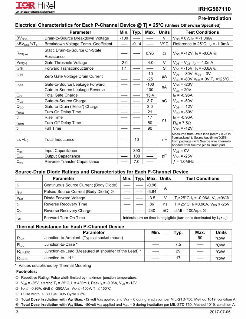
Electrical Characteristics for Each P-Channel Device @ Tj = 25°C (Unless Otherwise Specified)
Parameter Min. Typ. Max. Units Test Conditions BVDSS Drain-to-Source Breakdown Voltage -100 ––– ––– V VGS = 0V, ID = -1.0mA BVDSS/TJ Breakdown Voltage Temp. Coefficient ––– -0.14 ––– V/°C Reference to 25°C, ID = -1.0mA
RDS(on) Static Drain-to-Source On-State
––– ––– 0.96 Resistance
VGS(th) Gate Threshold Voltage -2.0 ––– -4.0 V VDS = VGS, ID = -1.0mA Gfs Forward Transconductance 1.1 ––– ––– S VDS = -15V, ID = -0.6A IDSS Zero Gate Voltage Drain Current
––– ––– -10 µA
VDS = -80V, VGS = 0V ––– ––– -25 VDS = -80V,VGS = 0V,TJ =125°C
IGSS Gate-to-Source Leakage Forward ––– ––– -100 nA
VGS = -20V Gate-to-Source Leakage Reverse ––– ––– 100 VGS = 20V
QG Total Gate Charge ––– ––– 13.4
nC
ID = -0.96A
QGS Gate-to-Source Charge ––– ––– 3.7 VDS = -50V
QGD Gate-to-Drain (‘Miller’) Charge ––– ––– 3.0 VGS = -12V td(on) Turn-On Delay Time ––– ––– 21
ns
VDD = -50V tr Rise Time ––– ––– 17 ID = -0.96A td(off) Turn-Off Delay Time ––– ––– 50 RG = 7.5 tf Fall Time ––– ––– 90 VGS = -12V
Ls +LD Total Inductance ––– 10 ––– nH
Measured from Drain lead (6mm / 0.25 in from package) to Source lead (6mm/ 0.25 in from package) with Source wire internally bonded from Source pin to Drain pad
Ciss Input Capacitance ––– 390 ––– pF
VGS = 0V Coss Output Capacitance ––– 100 ––– VDS = -25V Crss Reverse Transfer Capacitance ––– 7.0 ––– ƒ = 1.0MHz
VGS = -12V, ID = -0.6A
Source-Drain Diode Ratings and Characteristics for Each P-Channel Device Parameter Min. Typ. Max. Units Test Conditions
IS Continuous Source Current (Body Diode) ––– ––– -0.96
ISM Pulsed Source Current (Body Diode) ––– ––– -3.84
VSD Diode Forward Voltage ––– ––– -3.5 V TJ=25°C,IS = -0.96A, VGS=0V
trr Reverse Recovery Time ––– ––– 86 ns TJ=25°C, IF =0.96A, VDD ≤-25V
Qrr Reverse Recovery Charge ––– ––– 240 nC di/dt = 100A/µs
ton Forward Turn-On Time Intrinsic turn-on time is negligible (turn-on is dominated by LS+LD)
A
Footnotes:
Repetitive Rating; Pulse width limited by maximum junction temperature.
VDD = -25V, starting TJ = 25°C, L = 430mH, Peak IL = -0.96A, VGS = -12V
ISD -0.96A, di/dt -290A/µs, VDD -100V, TJ 150°C
Pulse width 300 µs; Duty Cycle 2%
Total Dose Irradiation with VGS Bias. -12 volt VGS applied and VDS = 0 during irradiation per MIL-STD-750, Method 1019, condition A.
Total Dose Irradiation with VDS Bias. -80volt VDS applied and VGS = 0 during irradiation per MlL-STD-750, Method 1019, condition A.
Thermal Resistance for Each P-Channel Device Parameter Min. Typ. Max. Units
RJA Junction-to-Ambient (Typical socket mount) ––– ––– 90 °C/W
RJC Junction-to-Case * ––– 7.5 ––– °C/W
RJ-LEAD Junction-to-Lead (Measured at shoulder of the Lead) * ––– 29 ––– °C/W
RJ-LID Junction-to-Lid * ––– 17 ––– °C/W
* Values established by Thermal Modeling
4 2017-07-05
IRHG567110
Pre-Irradiation
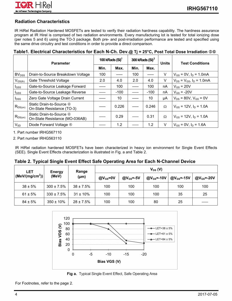
Table1. Electrical Characteristics for Each N-Ch. Dev.@ Tj = 25°C, Post Total Dose Irradiation
Parameter 100 kRads (Si)1
Units Test Conditions Min. Max. Min. Max.
BVDSS Drain-to-Source Breakdown Voltage 100 ––– 100 ––– V VGS = 0V, ID = 1.0mA
VGS(th) Gate Threshold Voltage 2.0 4.0 2.0 4.0 V VDS = VGS, ID = 1.0mA
IGSS Gate-to-Source Leakage Forward ––– 100 ––– 100 nA VGS = 20V
IGSS Gate-to-Source Leakage Reverse ––– -100 ––– -100 nA VGS = -20V
IDSS Zero Gate Voltage Drain Current ––– 10 ––– 10 µA VDS = 80V, VGS = 0V
RDS(on) Static Drain-to-Source On-State Resistance (TO-3)
––– 0.226 ––– 0.246 VGS = 12V, ID = 1.0A
RDS(on) Static Drain-to-Source On-State Resistance (MO-036AB)
––– 0.29 ––– 0.31 VGS = 12V, ID = 1.0A
VSD Diode Forward Voltage ––– 1.2 ––– 1.2 V VGS = 0V, ID = 1.6A
300 kRads (Si) 2
Table 2. Typical Single Event Effect Safe Operating Area for Each N-Channel Device
LET (MeV/(mg/cm2))
Energy (MeV)
Range (µm)
VDS (V)
@VGS=0V @VGS=-5V @VGS=-10V @VGS=-15V @VGS=-20V
38 ± 5% 300 ± 7.5% 38 ± 7.5% 100 100 100 100 100
61 ± 5% 330 ± 7.5% 31 ± 10% 100 100 100 35 25
84 ± 5% 350 ± 10% 28 ± 7.5% 100 100 80 25 –––
1. Part number IRHG567110
IR HiRel radiation hardened MOSFETs have been characterized in heavy ion environment for Single Event Effects (SEE). Single Event Effects characterization is illustrated in Fig. a and Table 2.
Fig a. Typical Single Event Effect, Safe Operating Area
For Footnotes, refer to the page 2.
2. Part number IRHG563110
IR HiRel Radiation Hardened MOSFETs are tested to verify their radiation hardness capability. The hardness assurance program at IR Hirel is comprised of two radiation environments. Every manufacturing lot is tested for total ionizing dose (per notes 5 and 6) using the TO-3 package. Both pre- and post-irradiation performance are tested and specified using the same drive circuitry and test conditions in order to provide a direct comparison.
Radiation Characteristics
020406080
100120
-20-15-10-50
Bia
s V
DS
(V
)
Bias VGS (V)
LET=38 ± 5%
LET=61 ± 5%
LET=84 ± 5%
5 2017-07-05
IRHG567110
Pre-Irradiation
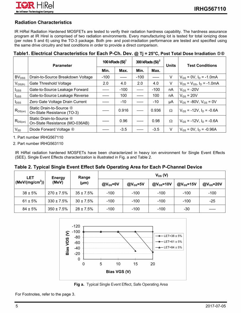
Table1. Electrical Characteristics for Each P-Ch. Dev. @ Tj = 25°C, Post Total Dose Irradiation
Parameter 100 kRads (Si)1
Units Test Conditions Min. Max. Min. Max.
BVDSS Drain-to-Source Breakdown Voltage -100 ––– -100 ––– V VGS = 0V, ID = -1.0mA
VGS(th) Gate Threshold Voltage 2.0 4.0 2.0 4.0 V VDS = VGS, ID = -1.0mA
IGSS Gate-to-Source Leakage Forward ––– -100 ––– -100 nA VGS = -20V
IGSS Gate-to-Source Leakage Reverse ––– 100 ––– 100 nA VGS = 20V
IDSS Zero Gate Voltage Drain Current ––– -10 ––– -10 µA VDS = -80V, VGS = 0V
RDS(on) Static Drain-to-Source On-State Resistance (TO-3)
––– 0.916 ––– 0.936 VGS = -12V, ID = -0.6A
RDS(on) Static Drain-to-Source On-State Resistance (MO-036AB)
––– 0.96 ––– 0.98 VGS = -12V, ID = -0.6A
VSD Diode Forward Voltage ––– -3.5 ––– -3.5 V VGS = 0V, ID = -0.96A
300 kRads (Si) 2
Table 2. Typical Single Event Effect Safe Operating Area for Each P-Channel Device
LET (MeV/(mg/cm2))
Energy (MeV)
Range (µm)
VDS (V)
@VGS=0V @VGS=5V @VGS=10V @VGS=15V @VGS=20V
38 ± 5% 270 ± 7.5% 35 ± 7.5% -100 -100 -100 -100 -100
61 ± 5% 330 ± 7.5% 30 ± 7.5% -100 -100 -100 -100 -25
84 ± 5% 350 ± 7.5% 28 ± 7.5% -100 -100 -100 -30 –––
1. Part number IRHG567110
IR HiRel radiation hardened MOSFETs have been characterized in heavy ion environment for Single Event Effects (SEE). Single Event Effects characterization is illustrated in Fig. a and Table 2.
Fig a. Typical Single Event Effect, Safe Operating Area
For Footnotes, refer to the page 3.
2. Part number IRHG563110
IR HiRel Radiation Hardened MOSFETs are tested to verify their radiation hardness capability. The hardness assurance program at IR Hirel is comprised of two radiation environments. Every manufacturing lot is tested for total ionizing dose (per notes 5 and 6) using the TO-3 package. Both pre- and post-irradiation performance are tested and specified using the same drive circuitry and test conditions in order to provide a direct comparison.
Radiation Characteristics
-120-100
-80-60-40-20
00 5 10 15 20
Bia
s V
DS
(V
)
Bias VGS (V)
LET=38 ± 5%
LET=61 ± 5%
LET=84 ± 5%
6 2017-07-05
IRHG567110
Pre-Irradiation
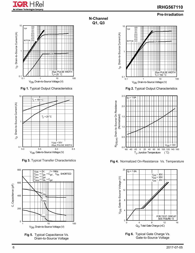
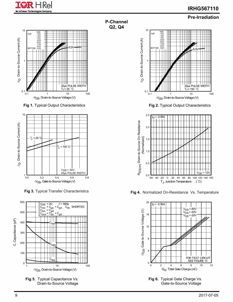
Fig 2. Typical Output Characteristics
Fig 3. Typical Transfer Characteristics
Fig 1. Typical Output Characteristics
Fig 4. Normalized On-Resistance Vs. Temperature
Fig 5. Typical Capacitance Vs. Drain-to-Source Voltage
Fig 6. Typical Gate Charge Vs. Gate-to-Source Voltage
0.1
1
10
0.1 1 10 100
20µs PULSE WIDTHT = 150 CJ °
TOP
BOTTOM
VGS15V12V10V9.0V8.0V7.0V6.0V5.0V
V , Drain-to-Source Voltage (V)
I ,
Dra
in-t
o-S
ou
rce
Cu
rre
nt (
A)
DS
D
5.0V
N-Channel Q1, Q3
0.1
1
10
0.1 1 10 100
20µs PULSE WIDTHT = 25 CJ °
TOP
BOTTOM
VGS15V12V10V9.0V8.0V7.0V6.0V5.0V
V , Drain-to-Source Voltage (V)
I ,
Dra
in-t
o-S
ou
rce
Cu
rre
nt (
A)
DS
D
5.0V
0.1
1
10
5.0 5.5 6.0 6.5
V = 50V20µs PULSE WIDTH
DS
V , Gate-to-Source Voltage (V)
I ,
Dra
in-t
o-S
ou
rce
Cu
rre
nt (
A)
GS
D
T = 25 CJ °
T = 150 CJ °
-60 -40 -20 0 20 40 60 80 100 120 140 1600.0
0.5
1.0
1.5
2.0
2.5
T , Junction Temperature ( C)
R
, D
rain
-to
-So
urc
e O
n R
esi
sta
nce
(No
rma
lize
d)
J
DS
(on)
°
V =
I =
GS
D
12V
1.6A
1 10 1000
200
400
600
800
V , Drain-to-Source Voltage (V)
C, C
ap
aci
tan
ce (
pF
)
DS
VCCC
====
0V,CCC
f = 1MHz+ C
+ C
C SHORTEDGSiss gs gd , dsrss gdoss ds gd
Ciss
Coss
Crss
0 4 8 12 160
4
8
12
16
20
Q , Total Gate Charge (nC)
V
, G
ate
-to
-So
urc
e V
olta
ge
(V
)
G
GS
FOR TEST CIRCUITSEE FIGURE
I =D
13
1.6A
V = 20VDS
V = 50VDS
V = 80VDS
7 2017-07-05
IRHG567110
Pre-Irradiation
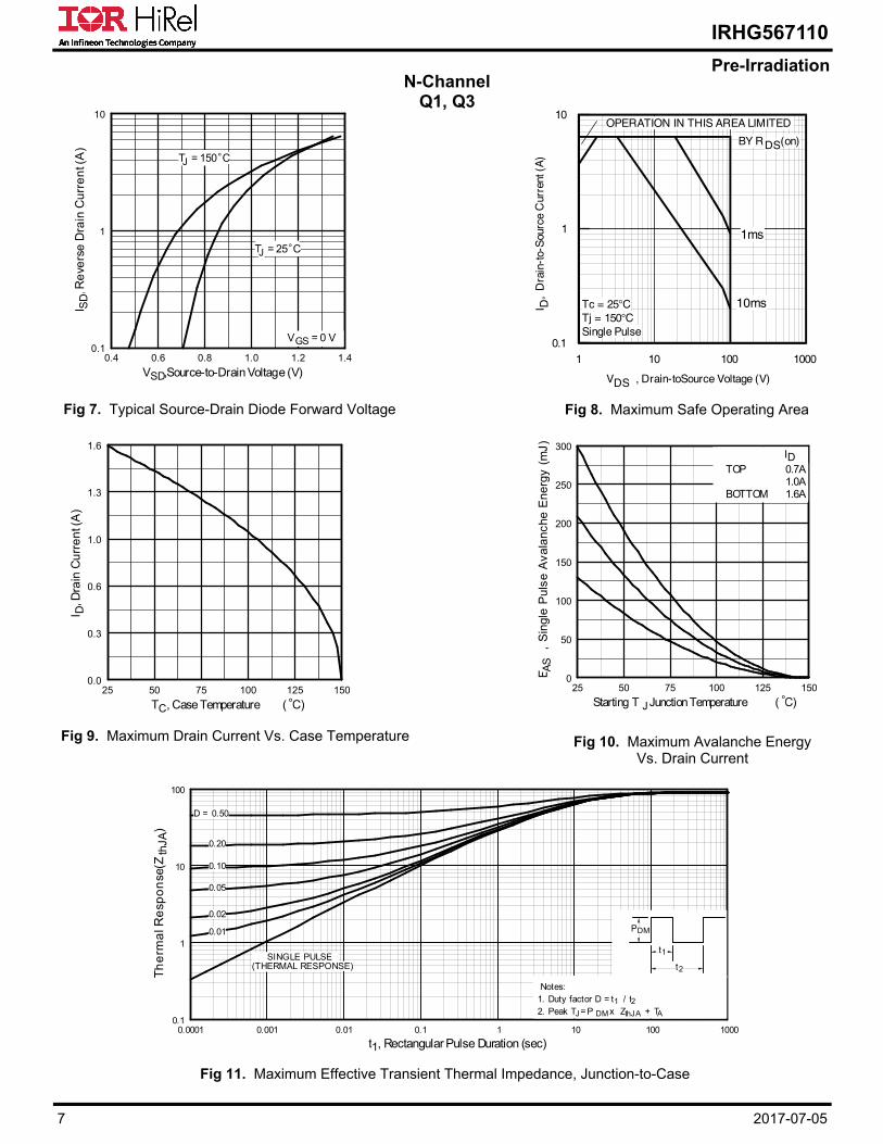
Fig 9. Maximum Drain Current Vs. Case Temperature
Fig 11. Maximum Effective Transient Thermal Impedance, Junction-to-Case
Fig 8. Maximum Safe Operating Area Fig 7. Typical Source-Drain Diode Forward Voltage
Fig 10. Maximum Avalanche Energy Vs. Drain Current
N-Channel Q1, Q3
1 10 100 1000
VDS , Drain-toSource Voltage (V)
0.1
1
10
I D,
Dra
in-t
o-S
ourc
e C
urre
nt (
A)
Tc = 25°CTj = 150°CSingle Pulse
1ms
10ms
OPERATION IN THIS AREA LIMITED
BY RDS(on)
0.1
1
10
0.4 0.6 0.8 1.0 1.2 1.4
V ,Source-to-Drain Voltage (V)
I
, Re
vers
e D
rain
Cu
rre
nt (
A)
SD
SD
V = 0 V GS
T = 25 CJ °
T = 150 CJ °
25 50 75 100 125 1500.0
0.3
0.6
1.0
1.3
1.6
T , Case Temperature ( C)
I ,
Dra
in C
urr
en
t (A
)
°C
D
25 50 75 100 125 1500
50
100
150
200
250
300
Starting T , Junction Temperature ( C)
E
,
Sin
gle
Pu
lse
Ava
lan
che
En
erg
y (m
J)
J
AS
°
ID
TOP
BOTTOM
0.7A 1.0A 1.6A
0.1
1
10
100
0.0001 0.001 0.01 0.1 1 10 100 1000
Notes:1. Duty factor D = t / t2. Peak T = P x Z + T
1 2
J DM thJA A
P t
t
DM
1
2
t , Rectangular Pulse Duration (sec)
Th
erm
al R
esp
on
se(Z
)
1
thJA
0.01
0.02
0.05
0.10
0.20
D = 0.50
SINGLE PULSE(THERMAL RESPONSE)
8 2017-07-05
IRHG567110
Pre-Irradiation
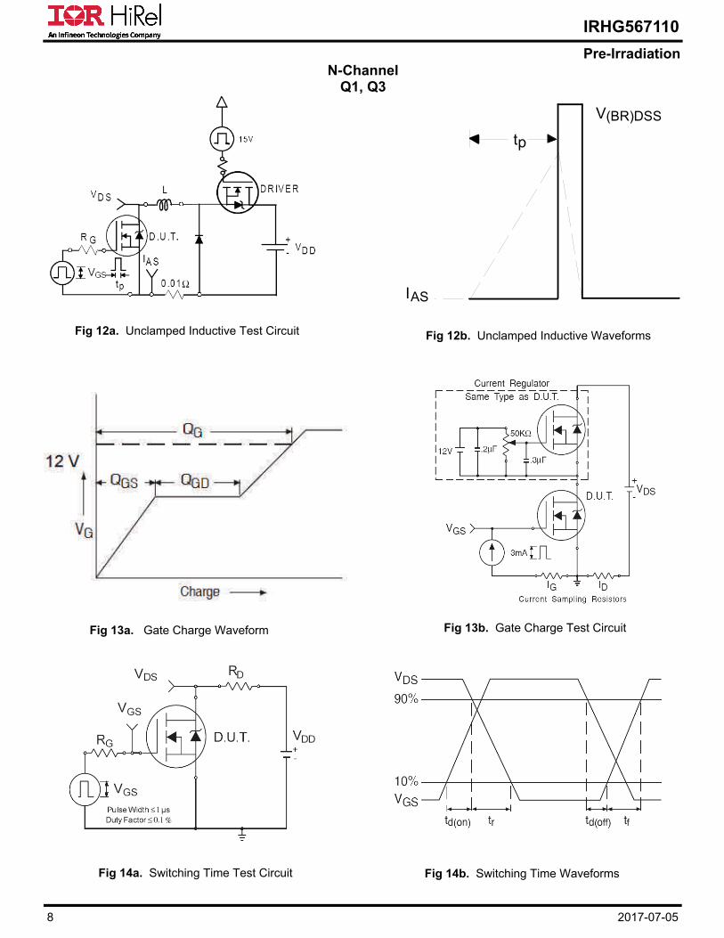
Fig 12a. Unclamped Inductive Test Circuit Fig 12b. Unclamped Inductive Waveforms
Fig 13b. Gate Charge Test Circuit Fig 13a. Gate Charge Waveform
Fig 14b. Switching Time Waveforms Fig 14a. Switching Time Test Circuit
tp
V(BR)DSS
IAS
N-Channel Q1, Q3
9 2017-07-05
IRHG567110
Pre-Irradiation
Fig 2. Typical Output Characteristics
Fig 3. Typical Transfer Characteristics
Fig 1. Typical Output Characteristics
Fig 4. Normalized On-Resistance Vs. Temperature
Fig 5. Typical Capacitance Vs. Drain-to-Source Voltage
Fig 6. Typical Gate Charge Vs. Gate-to-Source Voltage
P-Channel Q2, Q4
0.1
1
10
0.1 1 10 100
20µs PULSE WIDTHT = 25 CJ °
TOP
BOTTOM
VGS-15V-12V-10V-9.0V-8.0V-7.0V-6.0V-5.0V
-V , Drain-to-Source Voltage (V)
-I
, D
rain
-to
-So
urc
e C
urr
en
t (A
)
DS
D
-5.0V
0.1
1
10
0.1 1 10 100
20µs PULSE WIDTHT = 150 CJ °
TOP
BOTTOM
VGS-15V-12V-10V-9.0V-8.0V-7.0V-6.0V-5.0V
-V , Drain-to-Source Voltage (V)
-I
, D
rain
-to
-So
urc
e C
urr
en
t (A
)
DS
D
-5.0V
1
10
5.0 5.2 5.4 5.6 5.8
V = -50V20µs PULSE WIDTH
DS
-V , Gate-to-Source Voltage (V)
-I
, D
rain
-to
-So
urc
e C
urr
en
t (A
)
GS
D
T = 25 CJ °
T = 150 CJ °
-60 -40 -20 0 20 40 60 80 100 120 140 1600.0
0.5
1.0
1.5
2.0
2.5
T , Junction Temperature ( C)
R
, D
rain
-to
-So
urc
e O
n R
esi
sta
nce
(No
rma
lize
d)
J
DS
(on)
°
V =
I =
GS
D
-12V
-0.96A
1 10 1000
100
200
300
400
500
600
-V , Drain-to-Source Voltage (V)
C, C
ap
aci
tan
ce (
pF
)
DS
VCCC
====
0V,CCC
f = 1MHz+ C
+ C
C SHORTEDGSiss gs gd , dsrss gdoss ds gd
Crss
Coss
Ciss
0 2 4 6 8 10 120
4
8
12
16
20
Q , Total Gate Charge (nC)
-V
, G
ate
-to
-So
urc
e V
olta
ge
(V
)
G
GS
FOR TEST CIRCUITSEE FIGURE
I =D
13
-0.96A
V =-20VDS
V =-50VDS
V =-80VDS

10 2017-07-05
IRHG567110
Pre-Irradiation
Fig 9. Maximum Drain Current Vs. Case Temperature
Fig 11. Maximum Effective Transient Thermal Impedance, Junction-to-Case
Fig 8. Maximum Safe Operating Area Fig 7. Typical Source-Drain Diode Forward Voltage
Fig 10. Maximum Avalanche Energy Vs. Drain Current
0.1
1
10
100
0.0001 0.001 0.01 0.1 1 10 100 1000
Notes:1. Duty factor D = t / t2. Peak T = P x Z + T
1 2
J DM thJA A
P t
t
DM
1
2
t , Rectangular Pulse Duration (sec)
Th
erm
al R
esp
on
se(Z
)
1
thJA
0.01
0.02
0.05
0.10
0.20
D = 0.50
SINGLE PULSE(THERMAL RESPONSE)
P-Channel Q2, Q4
0.1
1
10
1.0 2.0 3.0 4.0 5.0
-V ,Source-to-Drain Voltage (V)
-I
, R
eve
rse
Dra
in C
urr
en
t (A
)
SD
SD
V = 0 V GS
T = 25 CJ °
T = 150 CJ °
1 10 100 1000
-VDS , Drain-toSource Voltage (V)
0.1
1
10
-ID
, D
rain
-to-
Sou
rce
Cur
rent
(A
)
Tc = 25°CTj = 150°CSingle Pulse
1ms
10ms
OPERATION IN THIS AREA LIMITED BY R DS(on)
25 50 75 100 125 1500
100
200
300
400
500
Starting T , Junction Temperature ( C)
E
, S
ing
le P
uls
e A
vala
nch
e E
ne
rgy
(mJ)
J
AS
°
ID
TOP
BOTTOM
-0.4A -0.6A
-0.96A
25 50 75 100 125 1500.0
0.2
0.4
0.6
0.8
1.0
T , Case Temperature ( C)
-I
, Dra
in C
urr
en
t (A
)
°C
D
11 2017-07-05
IRHG567110
Pre-Irradiation
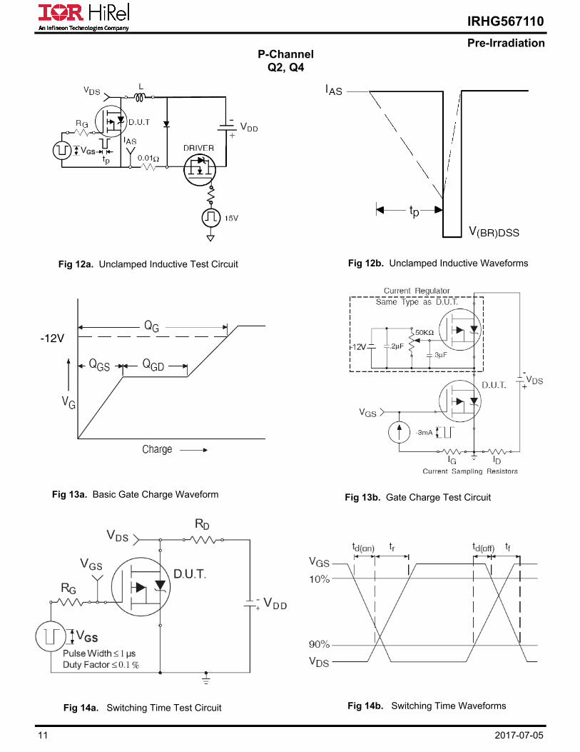
Fig 12a. Unclamped Inductive Test Circuit
Fig 13a. Basic Gate Charge Waveform
Fig 14b. Switching Time Waveforms Fig 14a. Switching Time Test Circuit
Fig 12b. Unclamped Inductive Waveforms
Fig 13b. Gate Charge Test Circuit
-12V
P-Channel Q2, Q4
12 2017-07-05
IRHG567110
Pre-Irradiation
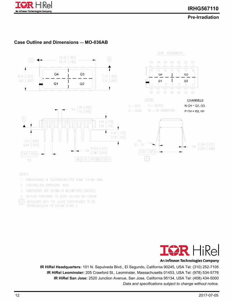
Case Outline and Dimensions — MO-036AB
IR HiRel Headquarters: 101 N. Sepulveda Blvd., El Segundo, California 90245, USA Tel: (310) 252-7105
IR HiRel Leominster: 205 Crawford St., Leominster, Massachusetts 01453, USA Tel: (978) 534-5776
IR HiRel San Jose: 2520 Junction Avenue, San Jose, California 95134, USA Tel: (408) 434-5000
Data and specifications subject to change without notice.
13 2017-07-05
IRHG567110
Pre-Irradiation
IMPORTANT NOTICE
The information given in this document shall be in no event regarded as guarantee of conditions or characteristic. The data contained herein is a characterization of the component based on internal standards and is intended to demonstrate and provide guidance for typical part performance. It will require further evaluation, qualification and analysis to determine suitability in the application environment to confirm compliance to your system requirements.
With respect to any example hints or any typical values stated herein and/or any information regarding the application of the product, Infineon Technologies hereby disclaims any and all warranties and liabilities of any kind including without limitation warranties on non- infringement of intellectual property rights and any third party.
In addition, any information given in this document is subject to customer’s compliance with its obligations stated in this document and any applicable legal requirements, norms and standards concerning customer’s product and any use of the product of Infineon Technologies in customer’s applications.
The data contained in this document is exclusively intended for technically trained staff. It is the responsibility of any customer’s technical departments to evaluate the suitability of the product for the intended applications and the completeness of the product information given in this document with respect to applications.
For further information on the product, technology, delivery terms and conditions and prices, please contact your local sales representative or go to (www.infineon.com/hirel).
WARNING
Due to technical requirements products may contain dangerous substances. For information on the types in question, please contact your nearest Infineon Technologies office.