Embed Size (px)
Citation preview

RADIO-FREQUENCY COMMUNICATION USING
HIGHER ORDER GAUSSIAN BEAMS
by
Haohan Yao
APPROVED BY SUPERVISORY COMMITTEE:
___________________________________________
Dr. Rashaunda M. Henderson, Chair
___________________________________________
Dr. Duncan L. MacFarlane
___________________________________________
Dr. Kamran Kiasaleh
___________________________________________
Dr. Andrew J. Blanchard

Copyright © 2018
Haohan Yao
All Rights Reserved

To Jingshuang Qiu, my wife and my true love.
To Zuming Yao and Fang Mo, my parents and my foundation.
To Dilan Yao, my little son and my wonder of wonders.
Words cannot express how much I love you all.

RADIO FREQUENCY COMMUNICATION USING
HIGHER ORDER GAUSSIAN BEAMS
by
HAOHAN YAO, BS, MS
DISSERTATION
Presented to the Faculty of
The University of Texas at Dallas
in Partial Fulfillment
of the Requirements
for the Degree of
DOCTOR OF PHILOSOPHY IN
ELECTRICAL ENGINEERING
THE UNIVERSITY OF TEXAS AT DALLAS
May 2018

v
ACKNOWLEDGEMENTS
Foremost, I would like to thank my advisor, Dr. Henderson, for the excellent guidance and the
immense support. I appreciate all her contributions of time, supervision, and funding to help me
complete my PhD degree and make my PhD experience productive.
I am greatly thankful to Dr. Duncan MacFarlane, Dr. Kamran Kiasaleh and Dr. Andrew Blanchard
for serving on my supervisory committee and providing insightful comments and suggestions.
I would like to thank Dr. Solyman Ashrafi and NxGen Partners for sustained support and research
suggestions.
I would like to thank Dr. Randall Lehmann and his son Drew Lehmann, for their time in providing
me their valuable feedback on my dissertation.
I would like to thank my loving wife, Jingshuang Qiu, for firmly standing beside me with love,
trust, and support all these years, encouraging and helping me proceed during my difficulty, and
sharing my joy during my success. Also, I would like to thank my dear parents, Zuming Yao and
Fang Mo, for giving me their unconditional support and encouragement.
Thanks goes to all professors, colleagues and friends who provided help and support to me. You
make me who I am today and may all share the credit of my happiness and achievements.
April 2018

vi
RADIO FREQUENCY COMMUNICATION USING
HIGHER ORDER GAUSSIAN BEAMS
Haohan Yao, PhD
The University of Texas at Dallas, 2018
S
Supervising Professor: Dr. Rashaunda M. Henderson
Recent explosive growth in the number of wireless devices and demand for portable information
content has led to the need for modern wireless systems with higher bandwidth to support faster
data rates. It is necessary to move to higher frequency bands to increase the channel capacity. It is
important to develop new methods to increase channel capacity for applications, including short
range chip-to-chip wireless links. One approach to increasing capacity that has been explored in
optics and at radio frequency (RF) is mode-division-multiplexing (MDM) of multiple orthogonal
electromagnetic beams.
This dissertation focuses on developing radio-frequency communication using higher order modes
of Gaussian beams, specifically Hermite-Gaussian (HG) and Laguerre-Gaussian (LG). First, a
physical phase plate was designed and fabricated to transform plane waves to Hermite-Gaussian
beams. The phase plate is designed for an HG11 mode, working at E-band from 71 to 76 GHz.
Second, an HG11 beam is formed using four inset-fed microstrip patch elements arranged with a
microstrip corporate feeding network at the same frequency. The physical phase plate and the patch
antenna array were both simulated using ANSYS HFSS. Radiation pattern measurements were

vii
taken on an NSI 700S-360 spherical near-field system at from 71 to 76 GHz with an Agilent vector
network analyzer (VNA). Third, LG beams were generated with spiral phase plates (SPP) from 71
to 76 GHz. Then a dual-channel E-band communication link using commercial impulse radios was
demonstrated with two LG beams over 2 meters range. LG OAM beams at E-band were also
generated by a circular patch array and then a wireless communication link was built using the
array to demonstrate twisting a wave with patches and untwisting it with a SPP. Also included is
a demonstration of horn antennas manufactured by 3D printing with low cost metallic paint for X-
band and Ka-band frequencies. This work advances wireless communication using advanced
hardware techniques.

viii
TABLE OF CONTENTS
ACKNOWLEDGMENTS ...............................................................................................................v
ABSTRACT ................................................................................................................................... vi
LIST OF FIGURES .........................................................................................................................x
LIST OF TABLES .........................................................................................................................xv
CHAPTER 1 INTRODUCTION ...................................................................................................1
1.1 Motivation ................................................................................................................1
1.2 Basic Concept of LG, HG ........................................................................................2
1.3 State of the Art on HG, LG RF/mm-wave Communications...................................7
1.4 Disseration Outline ..................................................................................................8
CHAPTER 2 GENERATION OF MILLIMETER-WAVE HERMITE-GAUSSIAN BEAMS
USING A PHYSICAL PHASE PLATE AND A PATCH ANTENNA ARRAY, .........................9
2.1 Introduction ..............................................................................................................9
2.2 HG11 Phase Plate Design and Fabrication .............................................................10
2.3 Simulation and Measurement Results ....................................................................13
2.4 Patch Antenna Design Theory ...............................................................................19
2.5 HG11 Patch Array Design and Working Mechanism .............................................22
2.6 Simulation and Measurement Results ....................................................................24
2.7 Conclusion .............................................................................................................30
CHAPTER 3 DEMONSTRATION OF OAM MULTIPLEXING USING COMMERCIAL
IMPULSE RADIOS WITH SPIRAL PHASE PLATE .................................................................32
3.1 Introduction ............................................................................................................32
3.2 Commercial Impulse Radio ...................................................................................33
3.3 Generation of LG Beams Using SPP .....................................................................35
3.4 Demonstration of E-band Link ..............................................................................39
3.5 Predictive Method Using MATLAB .....................................................................41
3.6 Twist and Untwist in MATLAB ............................................................................45
3.7 Conclusion .............................................................................................................47

ix
CHAPTER 4 EXPERIMENTAL DEMONSTRATION OF OAM MULTIPEXING USING
PATCH ANTENNA ARRAYS .....................................................................................................48
4.1 Introduction ............................................................................................................48
4.2 Demonstration of OAM Wireless Communication Link .......................................49
4.3 Conclusion .............................................................................................................56
CHAPTER 5 3D PRINTED HORN ANTENNA AT RADIO AND MILLIMETER WAVE
FREQUENCIES. ...........................................................................................................................57
5.1 Introduction ............................................................................................................57
5.2 3D Printing Techniques .........................................................................................58
5.3 Horn Antenna Theory ............................................................................................58
5.4 Ka-band Antenna 3D Model and Manufacturing ..................................................60
5.5 Ka-band Horn Simulation and Measurement Results ............................................62
5.6 X-band Antenna 3D Model and Manufacturing ....................................................68
5.7 X-band Horn Simulation and Measurement Results .............................................72
5.8 Conclusion .............................................................................................................77
CHAPTER 6 SUMMARY AND FUTURE WORK ...................................................................78
6.1 Summary ................................................................................................................78
6.2 Future Work ...........................................................................................................78
APPENDIX A COMPARISON GAIN MEASUREMENT USING NSI SCANNING
SYSTEM ........................................................................................................................................80
APPENDIX B SPHERICAL SCANNER USING ZVA MANUAL .............................................82
APPENDIX C OTHER TYPE HORN ANTENNAS ....................................................................85
REFERENCES ..............................................................................................................................88
BIOGRAPHICAL SKETCH .........................................................................................................94
CURRICULUM VITAE ................................................................................................................95

x
LIST OF FIGURES
Figure 1.1 Intensity and phase profiles of HG modes of different modes generated using
MATLAB. ............................................................................................................................4
Figure 1.2. Intensity and phase profiles of LG modes of different modes [23]. ..............................6
Figure 2.1. Geometry of HG11 mode: (a) HG11 intensity profile, (b) HG11 phase configuration. .10
Figure 2.2. (a) Dimensions of the fabricated E-band HG11 phase plate, (b) photograph of fabricated
laminated phase plate and (c) photograph of fabricated TOPAS phase plate. ...................11
Figure 2.3. Model of TOPAS HG11 phase plate in HFSS. .............................................................12
Figure 2.4. Simulated radiation pattern using HFSS with TOPAS phase plate at 73 GHz. ..........13
Figure 2.5. Measurement setup for radiation pattern measurement of HG11 on NSI System........14
Figure 2.6. Measured results: (a) normalized intensity distribution and (b) phase distribution of
HG11 physical phase plate. ................................................................................................15
Figure 2.7. Normalized radiation patterns at multiple frequencies of the HG11 TOPAS phase plate
measured using NSI system. ..............................................................................................16
Figure 2.8. Measured and simulated cuts of HG11 with TOPAS phase plate: (a) H-cut comparison,
(b) V-cut comparison and (c) -45o cut comparison. ...........................................................17
Figure 2.9. -45o cut showing the performance of the phase plate over multiple frequencies and with
different materials: (a) FR408, (b) laser cut and (c) waterjet cut. ......................................18
Figure 2.10. Inset-fed patch antenna dimension. ...........................................................................21
Figure 2.11. Simulated and measured reflection coefficient of the inset-fed patch. .....................21
Figure 2.12. Initial antenna array design and the phase placement. ..............................................22
Figure 2.13. Fabricated HG11 antenna array using FR408. ............................................................23
Figure 2.14. Measurement setup for radiation patterns of HG11 antenna array. ............................24
Figure 2.15. The placement for the fabricated patch array on AUT stand. ...................................25
Figure 2.16. Measured and simulated reflection coefficient of HG11 antenna array. ....................26

xi
Figure 2.17. Simulated normalized 3-D radiation pattern of HG11 antenna array at 73 GHz. ......27
Figure 2.18. Simulated vector of electric field of HG11 antenna array at 73GHz..........................27
Figure 2.19. Measured normalized 3-D radiation pattern of HG11 antenna array when the antenna
array is physically bent 90o. ...............................................................................................28
Figure 2.20. Simulated and measured 2-D normalized radiation pattern of HG11 antenna array at ϕ
= ±45°. ...............................................................................................................................29
Figure 2.21. Measured 3-D radiation patterns at multiple frequencies of HG11 antenna array. ...29
Figure 2.22. Measured phase distribution of HG11 antenna array. ...............................................30
Figure 2.23. Measured 2D radiation patterns at ϕ = 45°: (a) HG11 phase plate, and (b) HG11 patch
array. ..................................................................................................................................30
Figure 3.1. Impulse radio technology block diagram structure [41]. .............................................33
Figure 3.2. JDSU 6000 compact network test platform.................................................................34
Figure 3.3. Commercial impulse radio: (a) radio with 44 dBi Cassegrain antenna, (b) radio with
10 dBi SGH antenna. .........................................................................................................35
Figure 3.4. Fabricated SPP of l = 1 by Fedtech: (a) top view, (b) side view and (c) SPP in chamber
with SGH antenna. .............................................................................................................36
Figure 3.5. Measured 3D radiation patterns of l = 1 and l = 3. ......................................................37
Figure 3.6. Measured 2D radiation patterns: (a) l = 1 at phi = 0o and (b) l = 3 at phi = 0o. ...........38
Figure 3.7. Measured phase plots: (a) l = 1 and (b) l = 3 from NSI 2000. .....................................38
Figure 3.8. Setup block diagram for multiplexing and demultiplexing using two OAM beams. ..39
Figure 3.9. Photograph of the experiment setup. ...........................................................................40
Figure 3.10. Amplitude plot for LG beams, mode l = -1, Gaussian, l = +1, and l = +3 generated in
MATLAB. ..........................................................................................................................42
Figure 3.11. Phase plot for LG beams, mode l = -1, Gaussian, l = +1, and l = +3 generated in
MATLAB. ..........................................................................................................................43

xii
Figure 3.12. (a) Phase plot for untwisting LG beams, mode l=±1, l=±3 generated in MATLAB,
and (b) phase plot for untwisting LG beams, mode l=-1, l=+3 generated in MATLAB. .44
Figure 3.13. Measurement setup photo: (a) two phase plates combined under test, and (b) two
phase plates combined horn in details. ..............................................................................45
Figure 3.14. (a) Phase plot for untwisting LG beams, mode l=±1, l=±3 using SPPs, and (b) Phase
plot for sum of two LG modes, l=-1+3 = 2, using SPPs. ...................................................46
Figure 4.1. End launch connector connecting with an 8 element OAM l=-1 patch array. ............49
Figure 4.2. Block diagram of a wireless communication link using two SGHs. ...........................50
Figure 4.3. Photograph of a wireless communication link using two SGHs. ................................50
Figure 4.4. Geometry of OAM 𝑙 = −1 antenna array: (a) Initial antenna array design and phase
placement, (b) optimized array with feeding network, (c) single inset-fed patch
antenna. ..............................................................................................................................51
Figure 4.5. Simulated OAM 𝑙 = −1 patterns at 67 GHz: (a) 3D radiation pattern, and (b) 2D
radiation pattern at phi = 0o. ...............................................................................................52
Figure 4.6. Simulated OAM 𝑙 = −1 3D phase front at 67 GHz. ..................................................52
Figure 4.7. Diagram of OAM wireless communication link. ........................................................53
Figure 4.8. Photograph of the OAM l = +1 communication link setup: (a) front view, (b)
transmitting side and (c) receiving side. ............................................................................54
Figure 4.9. Received power shown on Spectrum Analyzer for OAM 𝑙 = −1 wireless
communication link. ..........................................................................................................55
Figure 5.1. Geometry of horn antenna designed in Solidworks. ...................................................60
Figure 5.2. Photograph of 20 dBi horn antennas: horn with Cu tape on the surface (A), horn with
Cu conductive paint (B) and reference standard gain horn (C). ........................................61
Figure 5.3. Photograph of measuring return loss of 3D printed horn antenna at Ka-band. ...........62
Figure 5.4. Measured return loss for 20 dBi horn antennas. ..........................................................63
Figure 5.5. Simulated 2D radiation patterns of different cases at 28 GHz: (a) ideal PEC model, (b)
Cu paint 3D printed 20 dBi horn, and (c) Cu tape 3D printed 20 dBi horn. ......................64

xiii
Figure 5.6. Measurement setup for radiation pattern: (a) overview, and (b) AUT test side view. 65
Figure 5.7. Measured 2D radiation patterns of different cases at 26 GHz: (a) Cu paint 3D printed
20 dBi horn, (b) Cu tape 3D printed 20 dBi horn and (c) reference SGH 20 dBi horn. ....67
Figure 5.8. Geometry of horn antenna designed in Solidworks. ...................................................68
Figure 5.9. Stratasys Fortus 400 3D Printing System. ...................................................................69
Figure 5.10. S-22 Microfinish Comparator....................................................................................70
Figure 5.11. HUSKY gravity spray gun ........................................................................................70
Figure 5.12. Photograph of 3D printed 15 dBi horn antenna with two layers of paint: profile view
(A), aperture view (B), and flange view (C). .....................................................................71
Figure 5.13. Photograph of 3D printed 15 dBi horn antennas: one layer copper paint horn (A), two
layers copper paint horn (B), three layers copper paint horn (C) and sliver paint horn
(D). .....................................................................................................................................71
Figure 5.14. Measurement setup for radiation pattern. ..................................................................72
Figure 5.15. Simulated 2D radiation patterns at 9.5 GHz: (a) XZ plane and (b) YZ plane. ..........73
Figure 5.16. Measured 2D radiation patterns at 9.5 GHz: (a) XZ plane, and (b) YZ plane. .........74
Figure 5.17. Measured peak gain over frequency. .........................................................................76
Figure 6.1. Block diagram of wireless link using patch arrays with OAM multiplexing. .............79
Figure A.1. Far-field plot setting in user window of NSI2000 software. ......................................80
Figure B.1. The trigger interface cable at the ZVA rear panel. .....................................................82
Figure B.2. Control wiring diagram. ..............................................................................................83
Figure B.3. PNA front panel connection. ......................................................................................83
Figure C.1. 3-D printed horn antennas using Stratasys Connex 3. ...............................................85
Figure C.2. 10 dB WR137 5.85 to 8.2 GHz waveguide 3-D printed copper paint horn with a
SMA Female input. ............................................................................................................85

xiv
Figure C.3. Far-field H-cut radiation pattern of 10 dB WR137 3-D printed copper paint horn at
6.5 GHz. .............................................................................................................................86
Figure C.4. 10 dB Ka-band Horns: (a) 3-D printed copper paint horn, (b) CNC Milling horn and
(c) Pasternack standard gain horn with waveguide to coax adapter. .................................86
Figure C.5. 10 dB Ka-band Horn Return Loss Comparison. .........................................................87
Figure C.6. Far-field H-cut radiation patterns comparison. ...........................................................87

xv
LIST OF TABLES
Table 3.1. Measured crosstalk and link BER .................................................................................41
Table 4.1. Wireless Communication System by OAM multiplexing ............................................48
Table 4.2. Power measurement for wireless communication system using SGH .........................48
Table 5.1. Dimensions of Ka-band horn antenna ..........................................................................60
Table 5.2 Summary of simulation and measurement.....................................................................66
Table 5.3. Dimensions of X-band horn antenna ............................................................................68
Table 5.4. Summary of measurement results .................................................................................75
Table 5.5. Summary of cost estimates ...........................................................................................76

1
CHAPTER 1
INTRODUCTION1
1.1 Motivation
The increase in use of mobile devices and portable electronics has led to strong traffic congestion
in the available wireless radio bands [1], and it is important to develop new methods to increase
channel capacity for applications including short range chip-to-chip wireless links. Such links
require low latency and high data rate [2]. One approach to increasing data rate and capacity that
has been explored in optics and at radio frequencies (RF) [3] is mode division multiplexing (MDM)
of electromagnetic beams with orbital angular momentum (OAM). In fiber optics and free space,
OAM beams such as the orthogonal Laguerre-Gaussian (LG) beams have been multiplexed
through the same spatial channel, thus increasing total channel capacity [4]–[6]. LG OAM
multiplexing is compatible with other existing multiplexing techniques, such as polarization
division multiplexing (PDM) and frequency or wavelength division multiplexing (FDM or WDM)
[7][8]. Therefore, beams with the same frequency and polarization can be reused by applying
different OAM modes to each beams, which enable a significantly potential increase in the channel
capacity [9].
Orthogonal LG OAM beams are not the only orthogonal set of modes that can be used for efficient
multiplexing and de-multiplexing of multiple data streams over the same channel. Hermite-
1 © 2016 IEEE. Reprinted, with permission, from H. Yao, H. Kumar, T. Ei, N. Ashrafi, T.LaFave Jr., S. Ashrafi, D.L. MacFarlane, R. Henderson, Patch antenna array for the generation of millimeter-wave Hermite-Gaussian beams, in IEEE Antennas and Wireless Propagation Letters, 2016.

2
Gaussian (HG) mode beams also have the potential to increase capacity in communication systems
by providing a complete orthogonal set in a plane transverse to the beams.
71-76 GHz, and 81-86 GHz bands are known as E-band. It is licensed and available worldwide.
This band offers a fiber-like high capacity (up to 3 Gbps) wireless point-to-point communication
solution. E-band wireless system are lower in cost than fiber, have 10 GHz of spectrum enabling
greater data rates, the longest transmission distances with robust weather resilience and have been
granted full interference protection [10].
This dissertation focuses on generating LG (OAM), HG using phase plates and patch antenna
arrays at E-band (71 to 76 GHz) for line of sight wireless communication. It also includes a study
of horn antennas at X band and Ka band that have been manufactured using low cost 3D printing
techniques.
1.2 Basic Concept of LG, HG
In optics, a Gaussian beam is collimated and expands as it propagates. It is a transverse
electromagnetic (TEM) mode [11]. To find the electric field amplitude of a Gaussian beam, we
must find the solution from the wave equation [12], [13].
∇2𝑈 −1
𝑐2
𝜕2𝑈
𝜕𝑡2 = 0 (1.1)
We introduce a trial solution
U(x, y, z, t) = u(𝑥, 𝑦, 𝑧)𝑒−𝑖𝑤𝑡 (1.2)
and replace it into equation (1.1), to produce the Helmholtz equation.
∇2𝑢 + 𝑘2𝑢 = 0 (1.3)

3
After making the paraxial approximation, which means that the field varies slowly with the
propagation direction z-axis, the resulting paraxial wave equation becomes:
𝜕2𝑢0
𝜕𝑥2+
𝜕2𝑢0
𝜕𝑦2+ 2𝑖𝑘
𝜕𝑢0
𝜕𝑧= 0 (1.4)
The mathematical expression of the Gaussian beam is the simplest solution to the paraxial wave
equation, given by [11], [14]:
𝐸(𝑟, 𝑧) = 𝐸0𝑤0
𝑤(𝑧)𝑒𝑥𝑝 (−
𝑟2
𝑤(𝑧)2) 𝑒𝑥𝑝 {−𝑖 [𝑘𝑧 + k
𝑟2
2𝑅(𝑧)− 𝜓(𝑧)]} (1.5)
where 𝑟 is the radial distance from the center axis of the beam, E0 is the peak amplitude, the beam
waist w0, the beam radius 𝑤(𝑧) = 𝑤0√1 + [𝜆𝑧/(𝜋𝑤02)], the wave number 𝑘 = 2𝜋/𝜆, the
Rayleigh length 𝑧𝑅 =𝜋𝑤0
2
𝜆, the radius of curvature 𝑅(𝑧) and the Gouy phase 𝜓(𝑧).
Hermite-Gaussian (HG) and Laguerre-Gaussian (LG) modes are higher-order modes of Gaussian
beams. HG modes are symmetric with respect to the Cartesian coordinate system [15] and LG
modes are circularly symmetric in nature expressed in cylindrical coordinates. LG modes
demonstrate vorticity [16]. Each LG or HG mode is orthogonal to one another [1], [17] leading to
the potential of increased channel capacity.
1.2.1 Hermite-Gaussian Beams
When one introduces functions in x, g(x,z) and y, h(y,z), there are solutions for g and h in terms
of Hermite polynomials in Cartesian coordinates [13]. Hermite polynomials are given by [18],
[19]:
𝐻𝑛(𝑥) = (2𝑥 −𝑑
𝑑𝑥)𝑛
∙ 1 (1.6)
with

4
𝐻0(𝑥) = 1, 𝐻1(𝑥) = 2𝑥, 𝐻2(𝑥) = 4𝑥2 − 2, …. (1.7)
The final solution is the approximation of the electric field distribution of an HG beam, given by
the product of a Gaussian function and a Hermite polynomial:
𝐻𝐺𝑛𝑚(𝑥, 𝑦, 𝑧) = 𝐸0𝑤0
𝑤(𝑧) . 𝐻𝑛 (√2
𝑥
𝑤(𝑧)) . 𝐻𝑚 (√2
𝑦
𝑤(𝑧)) . 𝑒𝑥𝑝 (−
𝑥2+𝑦2
𝑤(𝑧)2) . 𝑒𝑥𝑝 {−𝑖 [𝑘𝑧 − (1 + 𝑛 +
𝑚)𝑎𝑟𝑐𝑡𝑎𝑛𝑧
𝑧𝑅+
𝑘(𝑥2+𝑦2)
2𝑅(𝑧)]} (1.8)
With the peak amplitude E0, the beam waist w0, the beam radius 𝑤(𝑧) = 𝑤0√1 + [𝜆𝑧/(𝜋𝑤02)],
the Hermite polynomials of nth and mth order, the wave number 𝑘 = 2𝜋/𝜆, the Rayleigh
length 𝑧𝑅 =𝜋𝑤0
2
𝜆, and the radius of curvature 𝑅(𝑧). The integral number, n and m, of the Hermite
polynomials determine the shape of the HG profile in the x and y direction, respectively [14]. A
180° phase shift is required to generate a particular HG mode. The intensity and phase of different
HG modes with the same beam waist w0 is shown in Figure 1.1. Looking at the intensity profiles,
Figure 1.1. Intensity and phase profiles of HG modes of different modes generated using MATLAB.

5
a 180° phase shift is seen between the two light spots. This phase shift causes the null (dark line)
at the edge of the two adjacent light spots. The nulls (dark lines) determine the order of m and n,
HG modes.
1.2.2 Laguerre-Gaussian Beams
LG beam profiles are circularly symmetric and can be solved with the paraxial wave equation in
cylindrical coordinates using generalized Laguerre polynomials [13].
Laguerre polynomials are given by [19], [20]:
𝐿𝑛(𝑥) =1
𝑛!(
𝑑
𝑑𝑥− 1)
𝑛
𝑥𝑛 (1.9)
with
𝐿0(𝑥) = 1, 𝐿1(𝑥) = −𝑥 + 1, 𝐿2(𝑥) =1
2(𝑥2 − 4𝑥 + 2), …. (1.10)
The solution for the expression of Laguerre-Gaussian mode, is given by [21], [22],[23]:
𝐿𝐺𝑝𝑙 (𝑟, 𝜃, 𝑧) = 𝐸0
𝐾𝑙𝑝
𝑤(𝑧)(
𝑟√2
𝑤(𝑧))|𝑙|
× 𝑒−𝑖𝑙𝜃𝑒−(
𝑟
𝑤(𝑧))2𝐿𝑝|𝑙|
(2𝑟2
𝑤(𝑧))𝑒
−𝑖𝑘𝑟2
2𝑅(𝑧)𝑒−𝑖(2𝑝+|𝑙|+1)𝜓 (1.11)
In (1.11) 𝐸0 is the peak amplitude, 𝐾𝑙𝑝 = √2
𝜋
𝑝!
(1+𝑝)! is a normalization constant, l refers to the
mode of the LG beam which is an integer number, (p +1) is the number of radial nodes, R(z) is the
radius of curvature of the wave front and w is the width for which the Gaussian term falls to 1/e of
its own axis value. 𝜓 is the Gouy phase, which is an additional phase shift that differs from the

6
plane wave with the same optical frequency. 𝑒−𝑖𝑙𝜃 is the azimuthal phase term for the LG mode.
This term constitutes the orbital angular momentum (OAM) phase which creates the helical phase
front. The intensity and phase of different LG modes with the same beam waist w0 is shown in
Figure 1.2 [23]. Looking at the intensity profiles, when l≠0 and p=0 the beams have a single-ringed
“doughnut” between the two light spots, with the radius of doughnut proportional to 𝑙1/2. The
number of rings is proportional to p. The mode l stands for the phase delay of 2πl during one cycle
[24].
The azimuthal phase term of the LG mode constitutes the orbital angular momentum (OAM) phase
which creates the helical phase front. An electromagnetic (EM) wave has both OAM and spin
angular momentum (SAM). OAM is associated with the spatial distribution of the phase of the
fields while SAM corresponds to the wave polarization [25]. OAM and polarization are clearly
distinguished for a paraxial EM beam and can be considered as two independent properties of EM
Figure 1.2. Intensity and phase profiles of LG modes of different modes [23].
Figure 1.2.

7
waves [26], [27]. Therefore, all different modes are orthogonal to each other and independent to
the wave polarization [28].
1.3 State of the Art on HG, LG RF/mm-wave Communications
In the RF domain, an EM wave contains OAM modes that are usually not a pure LG mode, but an
infinite superposition of LG modes. An L𝐺0𝑙 beam with zero radial nodes (where 𝑝 = 0) can be
approximated to a general OAM beam with the same l mode with high efficiency [21]. There are
several methods to generate LG OAM beams in free space that have been demonstrated. One of
the most typical methods is to pass a radio beam through a spiral phase plate (SPP), where the
spiral surface forms a period of the helix [21]. Another one used a helicoidally parabolic antenna,
in which the helicoidal plate is treated as a vortex reflector [3]. Also, one method is to use an N-
element circular phased array, where all radiation elements are fed with the same signal but with
a specific phase shift [29]. Multiplexing data carrying OAM beams at the transmitter and
demultiplexing at the receiver has been demonstrated at optical [7], [8], [30], microwave [3], [31],
[32] and millimeter-wave bands [5], [33]–[35]. In [34], the authors used patch antenna arrays to
demonstrate a dual-channel wireless communication link at 60 GHz using two multiplexed OAM
modes at a short-range 15cm. Up to this point, there has been little work in E-band with point-to-
point wireless commercial communication systems using OAM to increase channel capacity.
HG mode beams also have the potential to increase capacity in communication systems by
providing a complete orthogonal set in a plane transverse to the beam [36]. By comparing the
spatial intensity distribution between LG and HG modes at a given point in the direction of
propagation, one can fit more HG modes into a given receiving aperture. It is possible to use more

8
structured HG mode patterns to encode more information compared to the LG mode [37]. In [38],
the authors compare mode-crosstalk and mode-dependent loss of LG modes and HG modes for
free-space optical communication. It was shown that some of the HG modes can experience less
mode-crosstalk and mode-dependent loss than LG modes. In the RF/mm-wave domain, the
concept of HG is novel compared to LG OAM and has not been explored. More research on theory
and practice needs to be developed and generating HG beams is an important fundamental step.
1.4 Dissertation Outline
Publications from this research work have been used to form the basis of this dissertation. This
dissertation is organized with the following structure: Chapter 2 presents two techniques for
generating mm-wave HG beams at E-band. Chapter 3 presents an experimental demonstration of
a dual-channel E-band communication link using commercial impulse radios with OAM
multiplexing and introduces a predictive method for analyzing OAM at RF/mm frequency. Chapter
4 presents circular patch arrays to generate LG OAM beams at E-band and an experimental
demonstration of an OAM wireless communication link with those arrays. Chapter 5 presents a
low-cost fast delivery technique for 3D printed horn antennas at radio and millimeter-wave
frequencies. The conclusion and future work are detailed in Chapter 6.
9
CHAPTER 2
GENERATION OF MILLIMETER-WAVE HERMITE-GAUSSIAN BEAMS USING A
PHYSICAL PHASE PLATE AND A PATCH ANTENNA ARRAY2, 3
2.1 Introduction
Multiplexing different orthogonal modes can potentially lead to an increase in data rates as more
information can be transmitted between radios within the same channel [1]. Hermite-Gaussian
(HG) mode beams have the potential to increase capacity in communication systems by providing
a complete orthogonal set in a plane transverse to the beam. HG beams have a higher number of
modes that can fit inside a given receiving aperture and are thought to be superior to Laguerre-
Gaussian (LG) beams. The concept of HG in RF is novel compared to OAM. Generating HG
beams is an important fundamental step for researching HG applications. This chapter presents
two techniques to generate millimeter-wave HG beams by using a designed physical phase plate
and by using a practical patch antenna array respectively. A HG11 phase plate was designed in E-
band using GNU plot, simulated in HFSS, fabricated and measured using a Nearfield Systems Inc.,
spherical near-field scanner. After that, an HG11 patch array was designed and simulated in HFSS.
The array was fabricated and measured across the band. Simulation and measurement of the phase
plate and patch array are both in agreement.
2 © 2016 IEEE. Reprinted, with permission, from H. Yao, H. Kumar, T. Ei, N. Ashrafi, T.LaFave Jr., S. Ashrafi, D.L. MacFarlane, R. Henderson, Patch antenna array for the generation of millimeter-wave Hermite-Gaussian beams, in IEEE Antennas and Wireless Propagation Letters, 2016.
3 © 2016 IEEE. Reprinted, with permission, from H. Kumar, H. Yao, T. Ei N. Ashrafi, T.LaFave Jr., S. Ashrafi, D.L. MacFarlane, R. Henderson, Physical phaseplate for the generation of a millimeter-wave Hermite-Gaussian beam, in IEEE RWS, 2016.

10
Two papers are utilized in this chapter. The author designed, simulated and fabricated HG11
physical phase plates and HG11 patch arrays. The author would like to thank H. Kumar, T. Ei and
R. Henderson for set up in measurements and efforts in characterization of physical phase plates
and patch arrays, along with sustained collaboration and research suggestions with N. Ashrafi, T.
LaFave Jr., S. Ashrafi and D.L. MacFarlane.
2.2 HG11 Phase Plate Design and Fabrication
The beam intensity and phase configuration for the HG11 mode are shown in Figure 2.1. There are
four distinct peaks (high intensity) with one horizontal null and one vertical null (low intensity).
The field of an HG beam undergoes a 180° phase shift across each null. Thus in the HG11 phase
plate there is a 180° phase difference between all adjacent quadrants of the phase plate.
Figure 2.2 shows the physical design of the HG11 phase plate for operation at 73 GHz. The
increased thickness of material in the two opposite quadrants is what introduces the 180° phase
shift needed for generating the HG11 beam. The length and width are dependent on the size of the
(a) (b)
Figure 2.1. Geometry of HG11 mode: (a) HG11 intensity profile, (b) HG11 phase configuration.

11
transmitting source and the transmit distance because the phase plates need to be large enough to
capture most of the beam. The aperture of the designed phase plate is 50.8 mm on a side. The
height profile is determined as a function of the wavelength, λ, and refractive index, n. The
wavelength at 73 GHz is 4.1 mm. The thickness of the phase plate, h, is calculated using:
h =λ
2π(n−1)arg(HGm
n ) (2.1)
where HGmn is the HG profile at the beam waist, w0, and ϕHG is the phase component of the HG
mode in far-field.
HGmn = Hm (√2
x
w0) exp (
−x2
w02 )Hn (√2
y
w0) exp (
−y2
w02 ) (2.2)
(a) (b)
(c)
Figure 2.2. (a) Dimensions of the fabricated E-band HG11 phase plate, (b) photograph of fabricated
laminated phase plate and (c) photograph of fabricated TOPAS phase plate.
12
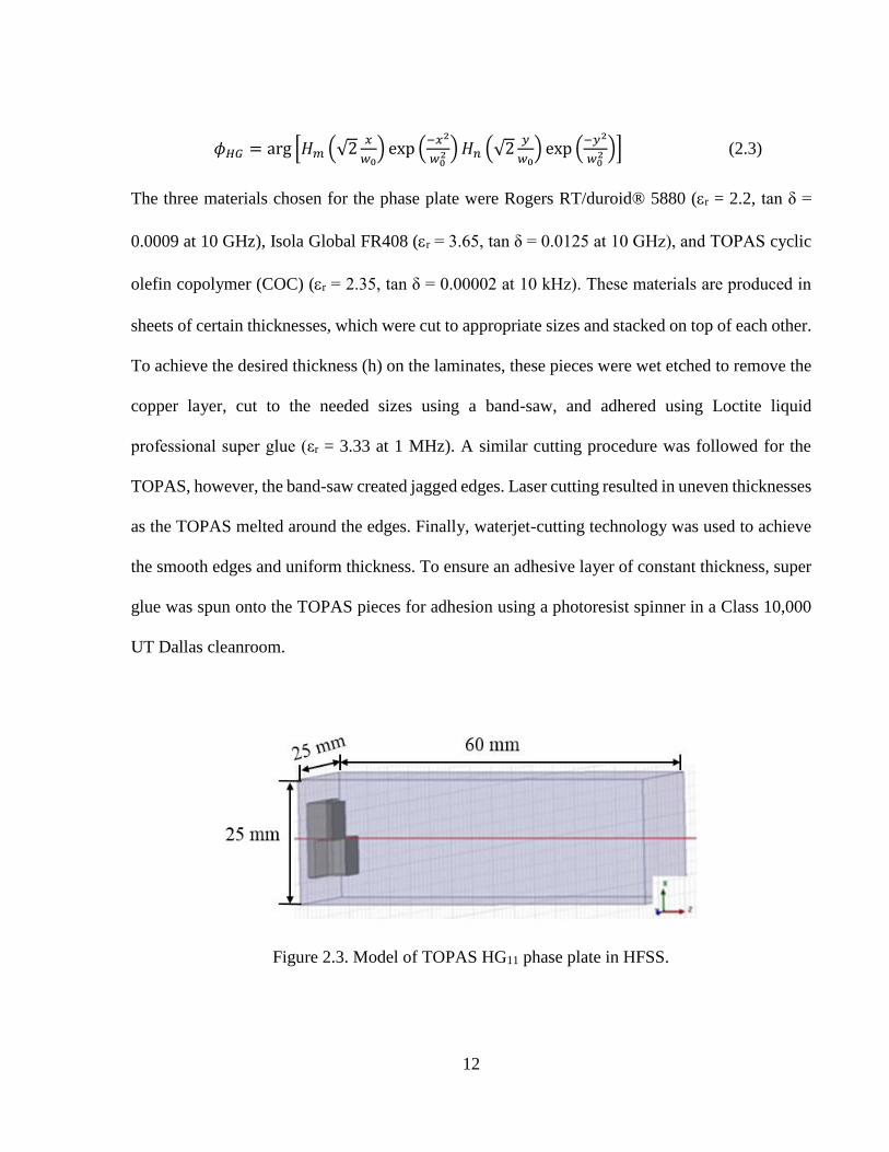
𝜙𝐻𝐺 = arg [𝐻𝑚 (√2𝑥
𝑤0) exp (
−𝑥2
𝑤02 )𝐻𝑛 (√2
𝑦
𝑤0) exp (
−𝑦2
𝑤02 )] (2.3)
The three materials chosen for the phase plate were Rogers RT/duroid® 5880 (r = 2.2, tan δ =
0.0009 at 10 GHz), Isola Global FR408 (r = 3.65, tan δ = 0.0125 at 10 GHz), and TOPAS cyclic
olefin copolymer (COC) (r = 2.35, tan δ = 0.00002 at 10 kHz). These materials are produced in
sheets of certain thicknesses, which were cut to appropriate sizes and stacked on top of each other.
To achieve the desired thickness (h) on the laminates, these pieces were wet etched to remove the
copper layer, cut to the needed sizes using a band-saw, and adhered using Loctite liquid
professional super glue (εr = 3.33 at 1 MHz). A similar cutting procedure was followed for the
TOPAS, however, the band-saw created jagged edges. Laser cutting resulted in uneven thicknesses
as the TOPAS melted around the edges. Finally, waterjet-cutting technology was used to achieve
the smooth edges and uniform thickness. To ensure an adhesive layer of constant thickness, super
glue was spun onto the TOPAS pieces for adhesion using a photoresist spinner in a Class 10,000
UT Dallas cleanroom.
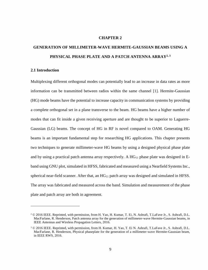
Figure 2.3. Model of TOPAS HG11 phase plate in HFSS.

13
2.3 Simulation and Measurement Results
The simulations were performed with ANSYS HFSS and the measurements were taken using
NSI’s near-field spherical scanner.
2.3.1 Simulation
Figure 2.3 shows the HG11 TOPAS phase plate with step difference of h=4.1 mm. In order to
reduce the simulation time, the size of the phase plate is 15 mm x 15mm modeled in HFSS instead
of 50.8mm x 50.8mm. The size of the air box is 25mm x 25mm x 60mm. The excitation source
used is a wave port generating an ideal plane wave. Plotted in Figure 2.4 is the radiation pattern of
the wave having passed through the phase plate. Most of the energy is focused in the four distinct
peaks as expected of the HG11 beam.
Figure 2.4. Simulated radiation pattern using HFSS with TOPAS phase plate at 73 GHz.

14
2.3.2 Measurement
The HG mode generated by the physical phase plate was characterized using the NSI 700S-360,
in an anechoic chamber with an Agilent E8361C PNA with Oleson OML 67-110 GHz modules.
This system measures the radiation pattern of a stationary antenna-under-test (AUT) using a multi-
axis high accuracy stepper motor positioning system [39]. The transmitting source used was a 10
dB WR-12 standard gain horn antenna (from Millimeter Wave Products, Inc). The phase plate was
placed in the far-field region of the horn, 100 mm from the horn aperture, to ensure plane wave
excitation. Equation (2.4) was used to calculate the far-field point.
𝑅 =2𝐷2
𝜆 (2.4)
where D is the largest dimension of the horn aperture – the diagonal 5.8 mm. A Bosch 5-point
laser-tracking tool was used to align the antenna, the phase plate, and the receiver.
Figure 2.5 shows the measurement setup for the NSI system. The phase plate was attached to a
Figure 2.5. Measurement setup for radiation pattern measurement of HG11 on NSI System.

15
6.25 mm thick, Rohacell® 71 HF holder (r = 1.093, tan δ = 0.0155 at 26.5 GHz) using double-
sided tape. Care was taken to ensure the center of the phase plate was aligned to the center of the
transmit horn. The receiver probe used was a 25dB standard gain horn antenna. A near field scan
of the radiation pattern was taken and the data was converted to far field using the NSI2000
software.
Figure 2.6 shows the measured intensity distribution and phase front at 73.5 GHz. Figure 2.7 shows
the normalized radiation pattern measured at the multiple frequencies using the waterjet-cut
TOPAS phase plate. The pattern agrees with the simulation where the 4 peaks are distinctly visible.
Figure 2.8 compares different cuts of the measurement to the simulation. For the HG11 mode, the
-45° cuts show the peaks, while, the 0° (H-cut) and the 90° (V-cut) show the nulls. Due to the
limitation of the measurement system, the back-lobe radiation could not be measured. The arms of
the scanner would have come into contact with the AUT stand. Both the measured and simulated
(a) (b)
Figure 2.6. Measured results: (a) normalized intensity distribution and (b) phase distribution of
HG11 physical phase plate.

16
results have been normalized to the global plot. Comparing the measured front-lobe cuts to the
simulation shows that they are both in good agreement. Looking at the -45° cuts, there is a
difference of about 20 dB observed between the peaks and nulls in both the simulation and the
measurement. Looking at the H-cut and the V-cut, the signals are both low-intensity: 20dB below
the peaks. Discrepancies in the measured data may be attributed to the adhesive not being included
in the simulation.
Figure 2.7. Normalized radiation patterns at multiple frequencies of the HG11 TOPAS phase plate
measured using NSI system.

17
Figure 2.9 shows the performance of the Duroid/FR408, laser-cut TOPAS and the waterjet-cut
TOPAS at 71, 73.5, and 76GHz. Comparing the results, the waterjet-cut TOPAS phase plates have
the best-defined main lobes. The performance of the phase plate is consistent across the E-band
frequencies with minimal difference in the radiation pattern. Also, HG10 phase plate was fabricated
(a) (b)
(c)
Figure 2.8. Measured and simulated cuts of HG11 with TOPAS phase plate: (a) H-cut comparison,
(b) V-cut comparison and (c) -45o cut comparison,

18
using the same design method as the waterjet TOPAS. The measured radiation patterns were in
good agreement with simulated results too, although not included.
(a) (b)
(c)
Figure 2.9. -45o cut showing the performance of the phase plate over multiple frequencies and with
different materials: (a) FR408, (b) laser cut and (c) waterjet cut.

19
2.4 Patch Antenna Design Theory
Using patch antennas to generate HG beams is similar to the circular patch array to generate LG
beams in [29]. The patches were placed in a configuration array and fed with the same signal but
with different phase delay. This capability lends itself to miniaturization and has the potential for
low cost and compact applications that use line of sight communication links. Patch element design
is the first step to complete an HG patch array. Patch antennas consist of a very thin (t ≪ λ) metallic
strip placed a small fraction of a wavelength (h≪λ) above a ground plane. The strip and the ground
plane are separated by a dielectric substrate, as shown in [40]. The patch antenna consists of two
slots, each of width w and height y, and placed perpendicular to the feed line. The two slots are
separated by a half-wavelength transmission line. The electric field at the aperture of each slot can
be decomposed into x- and y- components. The y-components are out of phase and cancel out
because of the half-wavelength transmission line [40], [41].
The frequency of operation of the patch antenna is determined by the length L. The width W of
the patch controls the input impedance. Larger widths also can increase the bandwidth. The width
further controls the radiation pattern. The normalized far-field components for this antenna equals
to [42]:
𝐸𝜃 =sin(
𝑘𝑊sin𝜃sin𝜙
2)
𝑘𝑊 sin𝜃sin𝜙
2
cos (𝑘𝐿
2sin 𝜃 cos𝜙) cos𝜙 (2.4)
𝐸𝜙 = −sin(
𝑘𝑊sin𝜃sin𝜙
2)
𝑘𝑊sin𝜃sin𝜙
2
cos (𝑘𝐿
2sin 𝜃 cos𝜙) cos 𝜃 sin 𝜙 (2.5)
Where k is the free-space wavenumber, given by 2π/λ.

20
A fast approximated design method introduced by [41], shows that the length of the patch is
given by:
𝐿 ≈ 0.49𝜆0
√𝜀𝑟 (2.6)
The input impedance of the patch is given by:
𝑍𝐴 = 90𝜀𝑟2
𝜀𝑟−1(
𝐿
𝑊)2
(2.7)
In general, there are three methods to feed the patch: inset microstrip feed, a quarter-wavelength
transmission line feed and a probe feed. An inset microstrip feed is applied to the latter patch array
design because the inset feed is easier to combine in corporate feeding network at E-band. The
geometry of the inset fed patch is illustrated in Figure 2.10.
The input impedance of the inset fed patch scales as [43]:
𝑍𝐴(𝑑) = 𝑍𝐴𝑐𝑜𝑠4 (
𝜋𝑑
𝐿) (2.8)
where d is the distance from the feed point to the end of the patch. Using equations (2.6) to (2.8),
the design of a 100 ohm input impedance for an inset feed patch antenna centered at 73GHz was
completed. After optimization using HFSS, the inset feed antenna was fabricated in the UTD
cleaningroom. Figure 2.10 shows the dimension of the single inset-fed patch antenna. The
fabricated patch was printed on the top layer of an Isola Global FR408 substrate (𝜀𝑟 =
3.75, tan 𝜃 = 0.018 at 10 GHz, ℎ = 0.125 mm and 𝑡 = 0.012 mm). Simulated and measured S-
parameters are shown from 65 to 85 GHz in Figure 2.11. After measuring the fabricated patch
size, updated the patch model and resimulated S-parameters are also shown in Figure 2.11. One
can see that -10 dB bandwidth is 69.5 to 75 GHz and center frequency is 72 GHz, which are shifting

21
from the simulation. The differences are due to the fabrication tolerances and the substrate relative
permittivity variation.
Figure 2.10. Inset-fed patch antenna dimension.
Figure 2.11. Simulated and measured reflection coefficient of the inset-fed patch.
22
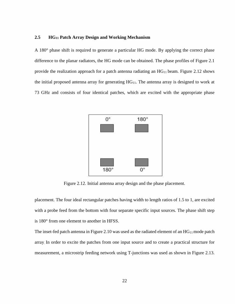
2.5 HG11 Patch Array Design and Working Mechanism
A 180° phase shift is required to generate a particular HG mode. By applying the correct phase
difference to the planar radiators, the HG mode can be obtained. The phase profiles of Figure 2.1
provide the realization approach for a patch antenna radiating an HG11 beam. Figure 2.12 shows
the initial proposed antenna array for generating HG11. The antenna array is designed to work at
73 GHz and consists of four identical patches, which are excited with the appropriate phase
placement. The four ideal rectangular patches having width to length ratios of 1.5 to 1, are excited
with a probe feed from the bottom with four separate specific input sources. The phase shift step
is 180° from one element to another in HFSS.
The inset-fed patch antenna in Figure 2.10 was used as the radiated element of an HG11 mode patch
array. In order to excite the patches from one input source and to create a practical structure for
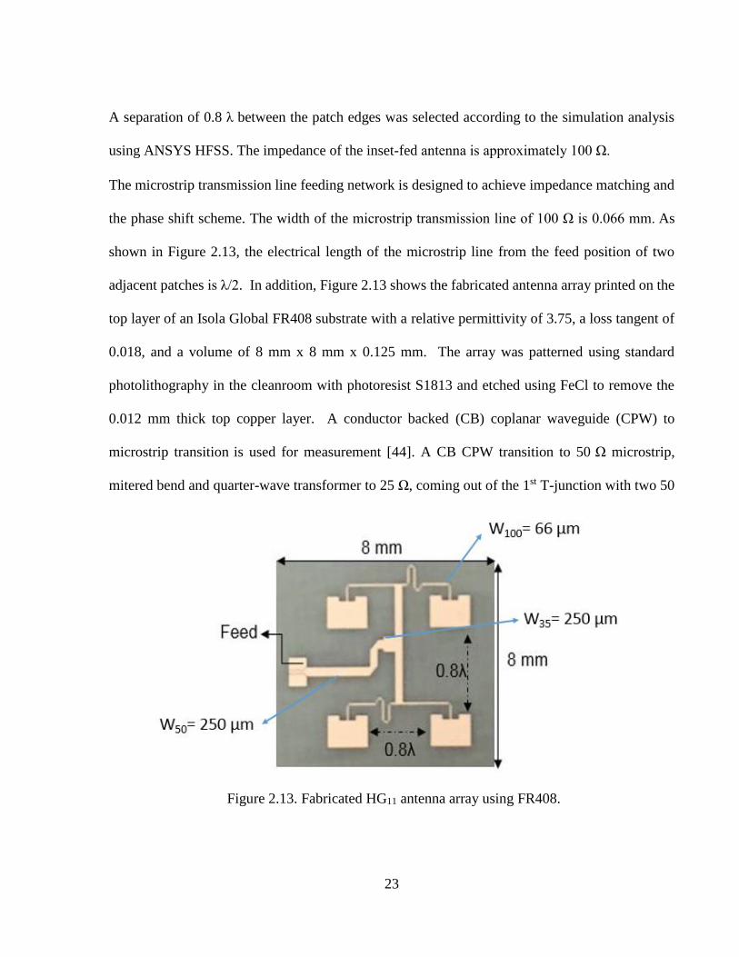
measurement, a microstrip feeding network using T-junctions was used as shown in Figure 2.13.
Figure 2.12. Initial antenna array design and the phase placement.
23
A separation of 0.8 λ between the patch edges was selected according to the simulation analysis
using ANSYS HFSS. The impedance of the inset-fed antenna is approximately 100 Ω.
The microstrip transmission line feeding network is designed to achieve impedance matching and
the phase shift scheme. The width of the microstrip transmission line of 100 Ω is 0.066 mm. As
shown in Figure 2.13, the electrical length of the microstrip line from the feed position of two
adjacent patches is λ/2. In addition, Figure 2.13 shows the fabricated antenna array printed on the
top layer of an Isola Global FR408 substrate with a relative permittivity of 3.75, a loss tangent of
0.018, and a volume of 8 mm x 8 mm x 0.125 mm. The array was patterned using standard
photolithography in the cleanroom with photoresist S1813 and etched using FeCl to remove the
0.012 mm thick top copper layer. A conductor backed (CB) coplanar waveguide (CPW) to
microstrip transition is used for measurement [44]. A CB CPW transition to 50 Ω microstrip,
mitered bend and quarter-wave transformer to 25 Ω, coming out of the 1st T-junction with two 50
Figure 2.13. Fabricated HG11 antenna array using FR408.

24
Ω arms and then two 100 Ω arms with a 180o delay line at 73 GHz to introduce the required phase
difference.
2.6 Simulation and Measurement Results
The antenna array radiation patterns were simulated using ANSYS HFSS and measured using
Agilent’s PNA (E8361A) and Oleson Microwave Labs’ OML module extenders were used to
measure the input return loss from 67 to 110 GHz. The antenna array was placed inside an anechoic
chamber and Nearfield System Inc.’s spherical near-field antenna scanner system, NSI 700S-360,
was used to measure the radiation pattern. Shown in Figure 2.14 and Figure 2.15 are the
measurement setup with the NSI scanner and probe feed, respectively.
Figure 2.14. Measurement setup for radiation patterns of HG11 antenna array.

25
2.6.1 S-Parameters
The S-Parameters were measured on a Cascade Microtech M150 probe station with a one-port
short open load (SOL) calibration. The simulated result includes a conductor-backed CPW to
microstrip transition modeled using AWR AXIEM. The measured and simulated S-parameters are
shown from 68 to 78 GHz in Figure 2.16. One can see that the -10 dB bandwidth is from 69.5 to
75 GHz, which is shifted from the simulation. The differences are due to the high frequency
limitations of the transition [9] and fabrication tolerances.
Double-sided tape was used to adhere the antenna onto the antenna under test (AUT) probe
platform, which was built using ten layers of Rohacell® 71 HF (r = 1.093, tan = 0.0155 at 26.5
GHz, t=6.25 mm). A ground-signal-ground (GSG) probe with a 150 µm pitch, manufactured by
MPI Corporation, was used to feed the structure. In order to capture the entire beam, a 20 mm long
Figure 2.15. The placement for the fabricated patch array on AUT stand.

26
feed was added to the antenna array. The array was physically bent 90°, as shown in Figure 2.15
[10]. Doing so ensured that the patch array was radiating in the direction of the receiver probe, and
the positioning of the AUT stand did not limit the measurement taken. Had the antenna been
designed without the 20 mm feed structure, the antenna would be radiating upwards and only
partial radiation patterns would have been captured. This arrangement is also required to obtain
the phase of the antenna array.
2.6.2 Radiation Patterns
The simulated 3-D patterns of the HG11 mode are shown in Figure. 2.17. Figure 2.18 shows the
simulated electric field vector of the antennas on the 8mm x 8mm observation area at 73 GHz, 5
mm away. One can see that the E-field magnitudes of patch 1 and patch 2 are almost the same
while the directions are opposite. The same results occur between patch 3 and patch 4. There are
some differences in the directions of the cross-pair patches, which is due to the coupling effect of
Figure 2.16. Measured and simulated reflection coefficient of HG11 antenna array.

27
the bend in the feeding network. The E-field magnitudes and directions are in agreement with the
HG11 mode shown in Figure 2.1. Figure 2.19 shows the measured results at 73.5 GHz when the
antenna array is physically bent 90°, as shown in Figure 2.16.
Figure 2.17. Simulated normalized 3-D radiation pattern of HG11 antenna array at 73 GHz.
Figure 2.18. Simulated vector of electric field of HG11 antenna array at 73 GHz

28
The four peaks, indicative of a HG11 beam, are observed and agree with the normalized co-
polarization E and H cuts at ± 45° angles as shown in Figure 2.20. The difference between the
peak and the null is about 8 dB from simulation results, and it is approximately 10 dB from
measured results. The simulated and measured radiation patterns are in good agreement, except
for a few differences due to variations in fabrication and measurement. Figure 2.21 shows 3D
radiation patterns at multiple frequencies and indicates the patch performance prevents a HG11
pattern at 83 GHz.
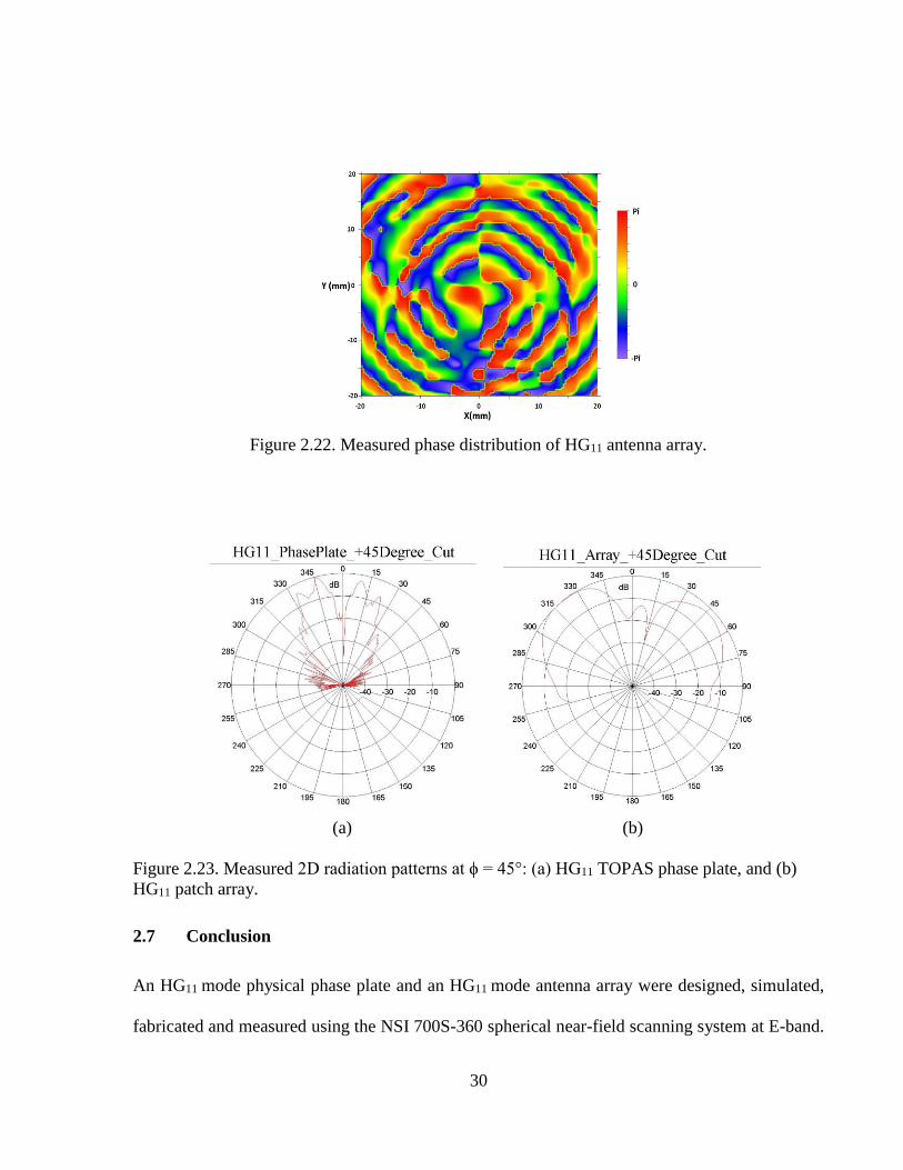
The measured phase distribution of the antenna, taken 5 mm away, is shown in Figure 2.22. One
can see that the phase of the cross-pair patches are approximately 0° phase around the center, while
the other pair are approximately 180° phase. This is in agreement with simulation and the HG11
Figure 2.19. Measured normalized 3-D radiation pattern of HG11 antenna array when the antenna
array is physically bent 90o.

29
mode theory. The peak value of the gain is 7.49 dB and the peak value of the directivity is 9.99 dB
from HFSS simulation results. Therefore, the radiation efficiency of the HG11 array calculated
from simulation is 56.3%.
Figure 2.20. Simulated and measured 2-D normalized radiation pattern of HG11 antenna array at
ϕ = ±45°.
-30
-25
-20
-15
-10
-5
0
0
30
120
150
180
210
240
270
300
330
Simulated Measured
Gai
n (
dB
)
45° Cut
-30
-25
-20
-15
-10
-5
0
0
30
120
150
180
210
240
270
300
330
Simulated Measured
Gai
n (
dB
)
-45° Cut
Figure 2.21. Measured 3-D radiation patterns at multiple frequencies of HG11 antenna array.
30
2.7 Conclusion
An HG11 mode physical phase plate and an HG11 mode antenna array were designed, simulated,
fabricated and measured using the NSI 700S-360 spherical near-field scanning system at E-band.
Figure 2.22. Measured phase distribution of HG11 antenna array.
(a) (b)
Figure 2.23. Measured 2D radiation patterns at ϕ = 45°: (a) HG11 TOPAS phase plate, and (b)
HG11 patch array.
Table 2.1. Wireless communication system by OAM multiplexing

31
The simulation and measured results are in good agreement with each other, confirming that both
a phase plate and an antenna array can generate an HG11 mode radio beam. Fig 2.23 shows the
measured 2D radiation patterns at ϕ = 45° for HG11 phase plate and patch array. The angle from
peak to peak is around 25o for phase plate while 60 o for patch array. The value from peak to null
is around 20 dB for phase plate while 16 dB for patch array. The reason is that applying a horn
with phase plate to generate HG11 mode and horn antenna has a higher directivity and narrower
beam width than the HG11 patch array. In general, both methods can produce HG11 mode in the
RF/mm-wave domain.

32
CHAPTER 3
DEMONSTRATION OF OAM MULTIPLEXING USING COMMERCIAL IMPULSE
RADIOS WITH SPIRAL PHASE PLATE4, 5
3.1 Introduction
In the optics community, Laguerre-Gaussian (LG) beams are higher orders of Gaussian beams
containing orbital angular momentum (OAM). An OAM based communication system is one
promising method that can increase the total channel capacity. The most typical method to generate
free-space Laguerre-Gaussian beams at millimeter-wave frequencies is by use of a spiral phase
plate [21]. This chapter focuses on the design, fabrication and characterization of spiral phase
plates (SPPs) to generate LG beams. Then commercial impulse radios are deployed with SPPs to
experimentally build a dual-channel E-band communication link with OAM multiplexing. Also, a
predictive method using MATLAB paraxial optics toolkit is introduced to synthesize and analyze
experimental results of multiplexing OAM modes at RF and mm-wave frequencies.
Two papers are utilized in this chapter. One paper focuses on an experimental demonstration using
commercial radios and the second focuses on developing a method in MATLAB to study
multiplexing. In the first published papers, the author measured and characterized the OAM spiral
phase plates. Also, he built the experimental demonstration setup, led and completed the
experimental demonstration. The author would like to thank H. Kumar, T. Ei, S. Sharma and R.
4 © 2017 IEEE. Reprinted, with permission, from H. Yao, H. Kumar, T. Ei, S. Sharma, R. Henderson, S. Ashrafi, D.L. MacFarlane, Z. Zhao, Y. Yan, A. Willner, Experimental demonstration of a dual-channel E-band communication link using commercial impulse radios with orbital angular momentum multiplexing, in IEEE RWS, 2017.
5 © 2017 IEEE. Reprinted, with permission, from S. Sharma, H. Yao, R. Henderson, S. Ashrafi, D.L. MacFarlane, Predictive method for analyzing OAM at radio frequencies, in Texas Symposium on WMCS, 2017.

33
Henderson for set up in measurements and efforts in alignment and implementation of the
experimental demonstration, along with sustained collaboration and research suggestions with S.
Ashrafi, D.L. MacFarlane, Z. Zhao and Y. Yan.
In the second published paper, the author completed the experimental setup for generating OAM
modes and the measurement of two phase plates. Also, he provided the theory suggestions to the
work. The author would like to thank S. Sharma for implementing the predictive method using the
MATLAB toolkit and R. Henderson for setup of measurement of OAM modes, along with
sustained collaboration and research suggestions with S. Ashrafi and D.L. MacFarlane.
3.2 Commercial Impulse Radio
Compared to the conventional radio technology, the impulse radio technology block diagram
(Figure 3.1) is much simpler without an up-and-down converter, which allows for size reduction,
low power consumption and low delay [45]. The input signal passes through the pulse generator
(PG) to generate the impulse signal. It is amplified by a wide-band high-power amplifier (W-
HPA), filtered by a band-pass filter (BPF) and then transmitted from the antenna. The impulse
wave beam is received by the RF receiver antenna and then amplified by a wide-band low-noise
Figure 3.1. Impulse radio technology block diagram structure.

34
amplifier (W-LNA). The envelope detector (DET) detects envelopes of the wide-band impulse
signal. Finally, a good shape of the signal is recovered with a limiter amplifier.
The E-band impulse radio used is shown in Figure 3.2. It is manufactured by Fujitsu. We connect
a 10 dBi standard gain horn (SGH) antenna with the transmit radio and a 44 dBi Cassegrain antenna
as described by Fujitsu for the receive radio. The frequency band is 71-76 GHz for the lower link
and 81-86 GHz for the upper link. The experimental demonstration covers the lower link only. The
transmission capacity is 3 Gb/s and Ethernet (10GbE or 1GbE) interfaces are supported [45]. In
order to complete the communication link test, four JDSU 6000 compact network test platforms
were rented and shown in Figure 3.3. This test unit can perform a 10GbE Ethernet local area
network (LAN) automatic test and measure bit-error-rate (BER), throughput, frame loss and packet
jitter testing of the communication channel [46].
Figure 3.2. Picture of JDSU 6000 compact network test platform.

35
3.3 Generation of LG Beams Using SPP
The SPP was used to generate LG beams because it is convenient to combine the impulse radio
with the SPP directly for indoor testing. According to [5], [21], a specific mode l of SPP has its
own step height, which is given by:
𝑆 =𝑙∙𝜆
𝑛−1 (3.1)
where 𝑆 is the step height, 𝑛 is the refractive index of the phase plate, 𝑙 is the state of the LG beam
and λ is the wavelength of the mm-wave beam. The SPP has one flat and one spiral surface. The
(a) (b)
Figure 3.3. Commercial impulse radio: (a) radio with 44 dBi Cassegrain antenna, (b) radio with
10 dBi SGH antenna.

36
thickness of the spiral surface varies azimuthally. High density polyethylene (HDPE) is used to
fabricate the SPP. It has a refractive index of about 1.52 at E-band. For the two modes of OAM
beams 𝑙 = 1 and 𝑙 = 3 were used for the experiment, where the step differences are 𝑆 = 7.9 𝑚𝑚
and 𝑆 = 23.7 𝑚𝑚, respectively. Fedtech made the HDPE SPPs. If one considers the clockwise
orientation of the spiral surface as positive modes, then the counterclockwise generates negative
modes. The SPPs were placed in an anechoic chamber (Figure 3.4) for characterization, using the
NSI 700S-360 scanning system and Keysight E8361C PNA with Oleson OML 67-110 GHz
modules. This system measures the radiation pattern of the plane wave after the SPP. Figure 3.4
shows the measurement setup. The phase plate was mounted on a Rohacell® 71 HF holder (r =
1.093, tan δ = 0.0155 at 26.5 GHz), 100 mm away from the horn aperture. The center of the SPP
was aligned to the center of the transmit horn antenna, a 10 dB WR-12 standard gain horn antenna.
(a)
(c)
(b)
Figure 3.4. Fabricated SPP of l = 1 by Fedtech: (a) top view, (b) side view and (c) SPP in
chamber with SGH antenna.

37
After taking a near field spherical scan measurement, the data was converted to the far field using
the NSI 2000 software.
The normalized measured radiation pattern for l = 1 and l = 3 are shown in Figure 3.5, which is
clearly a donut shape of the generated LG beams. Also, the radius of the center null part of 𝑙 = 1
is smaller than l = 3. Measured 2D radiation patterns are shown in Figure 3.6. The results indicate
that the beam width between the two peaks of the pattern for l = 1 is 16o while the beam width for
l = 3 is 28o. The phase plots of OAM mode l =+1, +3 are shown in Figure 3.7. We can see that l
=1 has one spiral while l=3 has three spirals in the phase plot. According to [3], [5], one can
Figure 3.5. Measured 3D radiation patterns of l = 1 and l = 3.

38
convert an OAM beam (l) of interest to a Gaussian-like beam of l = 0 with an inverse SPP (- l) and
the undesired OAM beam to another higher order OAM beam.
(a) (b)
Figure 3.6. Measured 2D radiation patterns: (a) l = 1 at phi = 0o and (b) l = 3 at phi = 0o.
(a) (b)
Figure 3.7. Measured phase plots: (a) l = 1 and (b) l = 3 from NSI 2000.

39
3.4 Demonstration of E-band Link
3.4.1 Experimental Setup
Figure 3.8 shows a free space dual-channel communication link using impulse radios with JDSU
compact test platforms and SPPs. The polarization of all antennas is the same. Radios 1 and 2 are
built as channel 1 while radios 3 and 4 as channel 2. Those two channels operate in the same range,
71 – 76 GHz with 3 Gbps data rate. At the transmitter, JDSU 1 and JDSU 2 generate two different
input test signals: A1 and A2. Those two input test signals are fed into impulse radio 1 and radio
3, respectively. SPPs l = +3 and l = -1 convert mm-wave data beams into OAM l = +3 and l = -1
respectively. Those two OAM beams are multiplexed using a 50:50 beam splitter (BS). The beam
splitter was designed using RSoft and fabricated by Sunstone Circuits. It is able to make half of a
beam pass through and reflect the other half, which has 3 dB loss. The combined OAM l = +3 and
l = -1 beams propagate along the free space path about 2 meters.
Figure 3.8. Setup block diagram for multiplexing and demultiplexing using two OAM beams.

40
At the receiver, a BS equally divides the combined beams. One half is passed through the reversed
SPP l = -3 and the other is passed through SPP l = +1. Those reversed SPPs convert the desired
OAM beam into Gaussian-like beams and the undesired OAM beam into another higher order
OAM beam, which allows one to demultiplex the desired OAM beam independently. The JDSU
2 generates the input signal A1 and compares it with the received signal to complete the
communication link test for channel 1. JDSU 4 completes the communication link test for channel
2 using the same method. Four HDPE lenses with a diameter of 30 cm are used to focus the mm-
wave beams and decrease the effect of divergence in free space. Absorbers are attached to the edge
of SPP and lenses in order to decrease the effect of reflection. A photo of the experimental setup
is shown in Figure 3.9.
3.4.2 Crosstalk and BER Measurements
The crosstalk of the OAM channel is measured by 𝑃𝑙 ≠ 𝑙1 / 𝑃𝑙 = 𝑙1
, where 𝑃𝑙 ≠ 𝑙1is the received power
of channel l1 when all channels except channel l1 are transmitting, and 𝑃𝑙 = 𝑙1 is the received power
Figure 3.9. Photograph of the experiment setup.

41
of channel l1 when only channel l1 is transmitting [5]. The received power can be directly read
from the user interface of radio 2 and radio 4. BER for each channel can be directly read from the
test reports of the JDSU when both channels are operating. Table 3.1 shows crosstalk and BER
results for channel 1 and channel 2. Received power was measured using software provided by
Fujitsu. The BER was measured with JDSU. Crosstalk for both channels is less than -15 dB. The
BER is very small for both channels. Alignment is critical for accurate measurements.
3.5 Predictive Method Using MATLAB
In optics, the amplitude, 𝐿𝐺𝑝𝑙 , of the LG beam in cylindrical co-ordinates is expressed
mathematically by [23]:
𝐿𝐺𝑝𝑙 (𝑟, 𝜃, 𝑧) = 𝐸0
𝐾𝑙𝑝
𝑤(𝑧)(
𝑟√2
𝑤(𝑧))|𝑙|
× 𝑒−𝑖𝑙𝜃𝑒−(
𝑟
𝑤(𝑧))2𝐿𝑝|𝑙|
(2𝑟2
𝑤(𝑧))𝑒
−𝑖𝑘𝑟2
2𝑅(𝑧)𝑒−𝑖(2𝑝+|𝑙|+1)𝜓 (3.2)
In (3.2) 𝐸0 is the peak amplitude, 𝐾𝑙𝑝 = √2
𝜋
𝑝!
(1+𝑝)! is a normalization constant, l refers to the mode
of the LG beam which is a integer number, (p +1) is the number of radial nodes, R(z) is the radius
of curvature of the wave front and w(z) is the width for which the Gaussian term falls to 1/e of its
own axis value. 𝜓 is the Gouy phase, which is an additional phase shift that differs from the plane
wave with the same optical frequency. 𝑒−𝑖𝑙𝜃 is the azimuthal phase term for the LG mode. This
term constitutes the OAM phase which creates the helical phase front.
Table 3.1. Measured crosstalk and link BER
Radio TX(dBm) Mode 𝑃𝑙 = +3 𝑃𝑙 = −1 Crosstalk(dB) BER
Channel 1
0 l = +3 -40 -55 -15 9.65x10⁻¹⁰
Channel 2
0 l = -1 -55 -39.5 -15.5 0
Figure 3.8. Photograph of the experiment setup.
Table 3.2. Measured crosstalk and link BER
Radio TX(dBm) Mode Crosstalk(dB) BER
Channel 1 0 l = +3 -15 9.65x10⁻¹⁰
Channel 2 0 l = -1 -15.5 0
Figure 3.8. Photograph of the experiment setup.
42
Using the basic paraxial optics toolkit in MATLAB [47], LG beams of different modes can be
generated. This toolkit adopts the equation of the LG beam from [48]. For generating OAM at 73
GHz some approximations are needed in the LG beam basic paraxial optics toolkit. The inputs to
the MATLAB toolkit are wavelength (λ), radius of curvature (R), number of radial nodes (p) and
LG mode (l). Approximations are made in order to compare the MATLAB generated beam to the
OAM wave generated using a horn antenna and spiral phase plate [5]. The horn antenna emits a
plane wave, which is twisted by the spiral phase plate creating a twisted plane wave. The width of
Figure 3.10. Amplitude plot for LG beams, mode l = -1, Gaussian, l = +1, and l = +3 generated
in MATLAB.

43
the beam (w) is set as the aperture of the spiral phase plate, which is 0.381 m. The wavelength at
73 GHz is 4.095 mm and the number of radial nodes is constant throughout the simulation, which
is considered as p =0. In MATLAB, the intensity and phase pattern for different LG modes can be
plotted after providing the required inputs. Figure 3.10 shows the amplitude of Gaussian and LG
modes using the MATLAB toolkit. Mode l = 0 represents a Gaussian beam which has no null at
the center of the intensity plot. For modes l =-1, +1, 3 the intensity pattern of the LG beam has a
Figure 3.11. Phase plot for LG beams, mode l = -1, Gaussian, l = +1, and l = +3 generated in
MATLAB.

44
null in its center resembling a donut. The size of the null is the same for l = ±1 and increases for l
= 3.
Figure 3.11 shows the phase plots of the modes depicted in Figure 3.10. The number of twists is
equal to the number of modes. From the phase plots, we can see that the direction of rotation the l
= -1 is opposite to that of the l = +1. The Gaussian approximations of the LG beams (l = 0) have a
constant phase at the center.
l=+1-1=0 l=+3-3=0
(a)
l=±1 l=±3
l=-1+3=2
(b)
Figure 3.12. (a) Phase plot for untwisting LG beams, mode l=±1, l=±3 generated in MATLAB,
and (b) phase plot for untwisting LG beams, mode l=-1, l=+3 generated in MATLAB.

45
3.6 Twist and Untwist in MATLAB
In Section 3.4 the experimental demonstration involved two plane waves that were twisted,
multiplexed in free space, received, untwisted and demultiplexed. Using MATLAB our goal is to
demonstrate the twisting and untwisting of modes. The untwisting of modes in MATLAB is done
by taking the convolution of the two modes. Theoretically, multiplication of l=±1 or l=±3 should
result in a zero phase. The azimuthal (OAM) phase term of (3.1) gets multiplied and gives l=0
mode. The multiplication of l=-1 and l=+3 should provide l=+2 mode. Figure 3.12 shows twist
and untwist LG beams using MATLAB. The phase plots are more descriptive than amplitude plots
as the mode generated can easily be decided by observing the number of twists in the phase plot.
(a) (b)
Figure 3.13. Measurement setup photo: (a) two phase plates combined under test, and (b) two
phase plates combined horn in details.

46
The multiplication of l=±1 or l=±3 has generated a constant phase at the center shown in Figure
3.12 (a). Figure 3.12 (b) shows the multiplication of l=-1 and l=+3 generate l=+2 mode.
The measured setup photo of combining modes (twisting and untwisting) is shown in Figure
3.13.The measured results of l=±1 and l=±3 using SPPs is shown in Figure 3.14 (a). The phase at
the center is zero. The phase plot of twisting and untwisting of modes l=±1, or l=±3 resembles the
phase plot of the standard gain horn antenna. This gives us confidence that the MATLAB LG beam
𝑙 = +1 − 1 = 0 𝑙 = +3 − 3 = 0
(a)
𝑙 = +1 − 1 = 0 𝑙 = +3 − 3 = 0
(a)
(b)
Figure 3.14. (a) Phase plot for untwisting LG beams, mode l=±1, l=±3 using SPPs, and (b) phase
plot for sum of two LG modes, l=-1+3 = 2, using SPPs.

47
toolkit can be useful in predicting how RF OAM modes interact. The phase plot for interaction of
l =-1 and l =3 using SPPs is shown in Figure 3.14 (b). As expected, it results in l= +2 mode, which
can be identified by the number of twists in the phase plot.
3.7 Conclusion
We successfully generated free space LG beams at E-band (71 –76 GHz) and experimentally
demonstrated that a dual-channel E-band (71 –76 GHz) communication link using commercial
impulse radios can be achieved with OAM multiplexing. The crosstalk and BER performance are
favorable for both channels. The experiment is limited to 2 meters but can be expanded once
alignment and received power issues are addressed. This work lends itself to the feasibility of
being able to increase channel capacity by the number of OAM modes. As for the predictive
method of analyzing OAM modes, the results obtained using MATLAB are in good agreement
with SPP experimental results. The physical implementation of adding a phase plate in front a
plane wave is equivalent to assigning the LG mode in optics using MATLAB. The mode of the
LG beam directly corresponds to the twist in the phase pattern. By twisting and untwisting l=±1
and l=±3 we obtained mode 0 using both methods. Combing l = -1 and l = +3 produces a LG beam
of mode l = -2. The predictive method capability is useful for experiments where all considerations
are accounted for twisting and untwisting OAM modes.

48
CHAPTER 4
EXPERIMENTAL DEMONSTRATION OF OAM COMMUNICATION USING PATCH
ANTENNA ARRAYS
4.1 Introduction
Recently OAM multiplexing has been demonstrated to improve the channel capacity at millimeter-
wave frequencies [5], [31], [33], [34], [35], [48]. One method to generate free-space OAM beams
at millimeter-wave frequencies is to use an N-element circular patch array to directly generate
OAM beams [29]. Authors in [29] described an eight element inset-fed circular phased array
antenna which can generate OAM radio beams at 10 GHz. Table 4.1 shows a summary of wireless
communication system with OAM multiplexing using patch arrays. This chapter focuses on the
experimental demonstration of building a free-space OAM communication link using patch
antenna arrays. A spectrum analyzer and a RF signal generator are deployed with OAM patch
antenna arrays. Also, it includes initial studies and simulation of an 8 element circular patch array
that has been used to generate OAM -1 at 73 GHz.
Table 4.1. Wireless communication system by OAM multiplexing
Reference Year Frequency Distance Tx side Rx side
[31] 2014 8.3 GHz 0.5 m
4 element array OAM +1
8 element array OAM+2
4 element array OAM -1
8 element array OAM-2
[34] 2016 60 GHz 0.15 m
4 element array OAM-1
8 element array OAM+2
SPP OAM +1 SPP OAM -2
Table 4.2. Wireless communication system by OAM multiplexing
Reference Year Frequency Distance Tx side Rx side
[31] 2014 8.3 GHz 0.5 m
4 element array OAM +1
8 element array OAM+2
4 element array OAM -1
8 element array OAM-2

49
4.2 Demonstration of OAM Wireless Communication Link
Simliar concepts for producing phase plates wirelss communication with the commericial radios
have been applied to demonstrate OAM wireless communication link using OAM circular patch
arrays. This demostration involves using continous wave signals generated with no modulation
scheme. The array factor of a circular patch array of N equally spaced element is given by [40] :
𝐴𝐹(𝜃, 𝜙) = ∑ 𝐼𝑛𝑒𝑗[𝑘𝑎 sin𝜃 cos(𝜙−𝜙𝑛)+𝛼𝑛]𝑁
𝑛=1 (4.1)
where 𝐼𝑛 is amplitude excitation of the nth element, 𝛼𝑛 is phase excitation of the nth element.
The array factor of an N-element circular antenna array carrying OAM mode, the nth element has
phase 𝜙𝑛 = 𝑙𝜑𝑛 where 𝜑𝑛 = 2𝜋𝑛/𝑁, is denoted by [50] :
𝐴𝐹(𝜃, 𝜑) = ∑ 𝑒−𝑗(𝑘∙𝑟𝑛−𝑙𝜑𝑛)𝑁𝑛=1 ≈ 𝑁𝑗−𝑙𝑒𝑗𝑙𝜑𝐽𝑙(𝑘𝑎 sin 𝜃) (4.2)
Note the azimuthal phase dependency, 𝑒𝑗𝑙𝜑, attributes to OAM mode.
Step 1 is generating RF signal. We are limited to either using a VNA or separate signal generators.
We uesd an Agilent E8257D signal generator that operates up to 67 GHz. A 1.85 mm cable and
Southwest Microwave end launch connector are used as opposed to the RF probe, shown in Figure
4.1.
Figure 4.1. End launch connector connecting with an 8 element OAM l=-1 patch array.

50
Step 2 involves completing a verification of system setup, we built a wireless communication link
using two standard gain horn antennas (SGH), shown in Figure 4.2 and Figure 4.3. Table 4.2 shows
Figure 4.2. Block diagram of a wireless communication link using two SGHs.
Figure 4.3. Photograph of a wireless communication link using two SGHs.
Table 4.2. Power measurement for wireless communication system using SGH
Pt (dBm) Pr (dBm) Distance (m) * Free space loss (dB) Noise floor(dBm)
10 -70 0.2 54.98 -80
14 -66 0.2 54.98 -80
* Aperture to aperture.
Figure 4.3. Photograph of a wireless communication link using two SGHs.
Figure 4.2. Photograph of a wireless communication link using two SGHs.

51
the power measured results.
Step 3 involves building an OAM wireless communication link. An 8 element OAM 𝑙 = −1 was
designed and simulated in HFSS (Figure 4.4). The array operates at 73GHz and consists of eight
identical patches.
(a) (b)
(c)
Figure 4.4. Geometry of OAM 𝑙 = −1 antenna array: (a) Initial antenna array design and phase
placement, (b) optimized array with feeding network, (c) single inset-fed patch antenna.

52
As shown in Figure 4.4a, the phase increment after a full cycle is 360o (2π) for the OAM mode l =
-1 and the phase shift step is 45 o from element to element. A microstrip feeding network using T-
\
(a) (b)
Figure 4.5. Simulated OAM 𝑙 = −1 patterns at 67 GHz: (a) 3D radiation pattern, and (b) 2D
radiation pattern at phi = 0o.
Figure 4.6. Simulated OAM 𝑙 = −1 3D phase front at 67 GHz.

53
junctions was designed to achieve this specific phase shift according to [29], [51]. Each element
is spaced approximately λ/2 apart and this amounts to a radius from the center feed structure of
1.25 λ according to the simulation optimization using ANSYS HFSS. The phase difference
between elements is achieved by orienting the patch in the opposite direction and adding different
feed transmission line length. The inset-fed patch was shown in Figure 4.4 (c).
The simulated 3D and 2D radiation patterns of OAM 𝑙 = −1 at 67 GHz are shown in Figure
4.5.The simulated radiation patterns did shown a null in the center and the difference between peak
and valley is about 20 dB. The simulated phase pattern is presented in Figure 4.6, where it shows
clearly seen that a twisted rotation phase distribution. It is concluded that an OAM 𝑙 = −1 beam
has been successfully generated at 67 GHz by the OAM 𝑙 = −1 circular patch array.
A free space OAM wireless communication link demonstration has been implemented using
fabricated OAM circular patch arrays (OAM 𝑙 = −1 and OAM 𝑙 = −3). Figure 4.7 shows the
Figure 4.7. Diagram of OAM wireless communication link.

54
diagram of the OAM communication link and Figure 4.8 shows the photograph of the OAM 𝑙 =
−1 wireless communication link experimental setup. Wood blocks, optical boards and angle
(a)
(a)
(b) (c)
Figure 4.8. Photograph of the OAM l = +1 communication link setup: (a) front view, (b)
transmitting side and (c) receiving side.
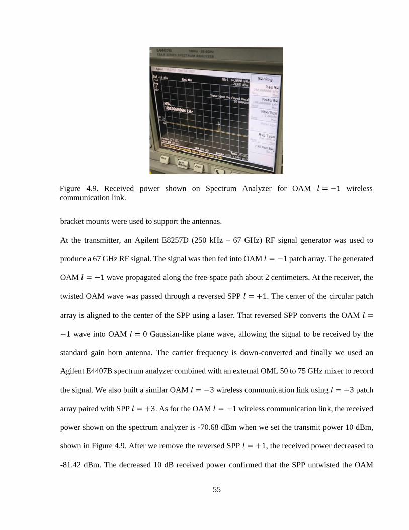
55
bracket mounts were used to support the antennas.
At the transmitter, an Agilent E8257D (250 kHz – 67 GHz) RF signal generator was used to
produce a 67 GHz RF signal. The signal was then fed into OAM 𝑙 = −1 patch array. The generated
OAM 𝑙 = −1 wave propagated along the free-space path about 2 centimeters. At the receiver, the
twisted OAM wave was passed through a reversed SPP 𝑙 = +1. The center of the circular patch
array is aligned to the center of the SPP using a laser. That reversed SPP converts the OAM 𝑙 =
−1 wave into OAM 𝑙 = 0 Gaussian-like plane wave, allowing the signal to be received by the
standard gain horn antenna. The carrier frequency is down-converted and finally we used an
Agilent E4407B spectrum analyzer combined with an external OML 50 to 75 GHz mixer to record
the signal. We also built a similar OAM 𝑙 = −3 wireless communication link using 𝑙 = −3 patch
array paired with SPP 𝑙 = +3. As for the OAM 𝑙 = −1 wireless communication link, the received
power shown on the spectrum analyzer is -70.68 dBm when we set the transmit power 10 dBm,
shown in Figure 4.9. After we remove the reversed SPP 𝑙 = +1, the received power decreased to
-81.42 dBm. The decreased 10 dB received power confirmed that the SPP untwisted the OAM
Figure 4.9. Received power shown on Spectrum Analyzer for OAM 𝑙 = −1 wireless
communication link.
Figure 4.7. Received power shown on Spectrum Analyzer for OAM 𝑙 = −1 wireless
communication link.

56
wave. For OAM -3 wireless communication link, the received power is -72.59 dBm with the
reversed SPP 𝑙 = +3 and is -75.28 dBm without the SPP. There is only 3 dBm difference for OAM
+3 link. One reason might be that the performance of 8-element OAM +3 patch array is worse than
OAM +1 patch array. Another reason might be that the OAM +3 wave diverges faster than OAM
+1. A final consideration is the bandwidth of the patch array is within the 71 to 76 GHz band
whereas this measurement is conducted at 67 GHz.
4.3 Conclusion
We experimentally demonstrate that OAM wireless communication link can be achieved with
OAM patch arrays (𝑙 = −1 and 𝑙 = −3 ). The OAM 𝑙 = −1 link is better than OAM 𝑙 = −3 link
based on measured crosstalk (received power with and without appropriate SPP). OAM 𝑙 = −1
beam has a better continuity of the phase profile and quality of radiation pattern than OAM 𝑙 =
−3. The number of the element of the array (eight for OAM 𝑙 = −1 and OAM 𝑙 = −3) and the
large transmission path loss and coupling effect due to the microstrip feeding network are major
factors which degrade the performance. The experiment is limited to 2 centimeters which is based
on the passive mixer at Rx side but can be expanded once alignment and received power issues
are addressed. This work might be beneficial for building OAM mm-wave communication link
based on circular patch arrays. I designed and simulated an 8-element OAM circular patch array
to generate OAM 𝑙 = −1 beam at E-band (71 to 76 GHz). The simulation results present a good
continuity of the phase profile and quality of radiation pattern of OAM 𝑙 = −1.

57
CHAPTER 5
3D PRINTED HORN ANTENNA AT RADIO AND MILLIMETER-WAVE
FREQUENCY6, 7
5.1 Introduction
For a point-to-point application where a high-directivity antenna is required, a horn would be a
good choice. As a low cost and fast delivery option, 3D printers can manufacture a horn antenna.
This chapter discusses a method using fused deposition modeling (FDM) 3D printing techniques
combined with metal spray deposition to determine the feasibility of fabricating horn antennas for
radio frequency (RF) point-to-point applications. Firstly, the spectrum at 28 GHz band is being
proposed for 5G communication [52]. In this work horns are 3D printed at 28 GHz and metallized
using two different metallization methods. In addition 3-D printing is used to realize horn antennas
at X-band (8-12 GHz) lower frequency band and evaluate radiation patterns and gain as a function
of metal thickness. The 3D model, simulation and measurement results will be described.
Two papers are utilized in this chapter. The author designed, simulated, metalized and measured
Ka-band 3D printed horn antennas and X-band 3D printed horn antennas. The author would like
to thank L. Fang, S. Sharma and R. Henderson for set up in measurements and efforts in
characterization of those Ka-band and X-band horn antennas, and sustained collaboration and
research suggestions from S. Ashrafi and D.L. MacFarlane.
6 © 2017 IEEE. Reprinted, with permission, from H. Yao, S. Sharma, R. Henderson, S. Ashrafi, D.L. MacFalane, Ka band 3D printed horn antennas, in Texas Symposium on WMCS, March 2017.
7 © 2018 IEEE. Reprinted, with permission, from H. Yao, L. Fang, R. Henderson, Evaluating conductive paint performance on 3-D printed horn antennas, in IEEE RWS, Jan. 2018.

58
5.2 3D Printing Techniques
Over the last 15 years, 3D printing, also known as additive manufacturing, has found widespread
applications for radio frequency systems [53]–[55]. 3D printing is a novel technology which
enables users to fabricate objects directly from a computer aided design (CAD) digital model.
Compared to traditional computer numerical control (CNC) machining technology, 3D printing
has the advantages of low cost and high efficiency [56]. One of the most common methods of 3-
D printing is fused deposition modeling (FDM). Applying the FDM process, melted thermoplastic
is extruded in small parts, which hardens instantaneously. Then many patterned layers are stacked
to form the 3D objects [57]. Stratasys fused deposition modeling 3-D printing is commonplace in
the university and industrial setting given its low setup cost and flexibility in realizing custom
structures for prototyping and low volume projects. FDM is used for dielectric structures ranging
from mechanical parts to electrical components. When considering 3-D printing for electrical
circuits and particularly the RF Front-end, the material loss properties for dielectric (loss tangent)
and metals (conductivity and surface roughness) should be considered [58].
5.3 Horn antenna theory
The horn is the simplest and the most widely used microwave and millimeter wave antenna. It
began in the late 1930s. Many of the articles and designs published since 1939 and designs of a
horn as a radiator can be found in a book of reprinted papers [40]. The horn antenna can provide
moderate to high gain, low return loss, wide bandwidth and is relatively easy to manufacture [59].

59
The most widely used horn is a pyramidal feed horn which is flared in both directions [40]. As for
pyramidal horn, the aperture field is affected by phase error in E-plane and H-plane. The tangential
components of the E- and H-field over the aperture of the horn is approximated by
�⃗� (𝑥, 𝑦) = 𝐸0 ∙ cos (𝜋∙𝑥
𝐴) ∙ 𝑒
−𝑗∙8∙𝜋∙𝑡∙ 𝑥2
𝐴2 ∙ 𝑒−𝑗∙8∙𝜋∙𝑠∙
𝑦2
𝐵2 ∙ �⃗� 𝑦 (6.1)
Where t is the phase error at the aperture in the H-plane; s is the phase error at the aperture in the
E-plane.
𝑡 =𝐴2
8∙𝜆∙𝜌𝐻 (6.2)
𝑠 =𝐵2
8∙𝜆∙𝜌𝐸 (6.3)
The maximum radiation of the pyramidal horn is directed nearly along the Z-axis. The directivity
for the pyramidal horn can be written by:
𝐷𝑝 = 𝜋
32∙ (
𝜆
𝐴∙ 𝐷𝐸) ∙ (
𝜆
𝐵∙ 𝐷𝐻) (6.4)
Where 𝐷𝐸 and 𝐷𝐻 are directivities of E-plane and H-plane sectoral horns as given by
𝐷𝐸 =64∙𝐴∙𝜌𝐸
𝜋∙𝜆∙𝐵∙ [𝐶2 (
𝐵
√2∙𝜆∙𝜌𝐸) + 𝑆2 (
𝐵
√2∙𝜆∙𝜌𝐸)] (6.5)
𝐷𝐻 =4∙𝜋∙𝐵∙𝜌𝐻
𝐴∙𝜆∙ {[𝐶(𝑢) − 𝐶(𝑣)]2 + [𝑆(𝑢) − 𝑆(𝑣)]2} (6.6)
Where
𝑢 =1
√2(√𝜆∙𝜌𝐻
𝐴+
𝐴
√𝜆∙𝜌𝐻) (6.7)
𝑣 =1
√2(√𝜆∙𝜌𝐻
𝐴−
𝐴
√𝜆∙𝜌𝐻) (6.8)
The effective aperture of these pyramidal feed-horns is around 50%, the gain can be related to its
physical size as given by

60
𝐺 = 𝜀𝑎𝑝 ∙4∙𝜋
𝜆2 ∙ 𝐴𝑝 =1
2∙4∙𝜋
𝜆2 ∙ (𝐴 ∙ 𝐵) (6.9)
5.4 Ka-band Antenna 3D Model and Manufacturing
The horn antenna is designed based on reference horns sold by Pasternack, antenna PE9850/2F-
20 [60]. The geometry of the antenna is shown in Figure 5.1, where A is the horn length, and B
and C are the inside aperture dimensions without considering that the dielectric thickness is
1.7mm. WR-28 waveguide dimensions are 7.11 mm × 3.56 mm. As listed in Table 5.1, the 20 dBi
horn is 27.8 mm × 36.8 mm with 79.4 mm length.
Figure 5.1. Geometry of horn antenna designed in Solidworks.
Figure 5.2. Geometry of horn antenna designed in Solidworks.
Figure 5.3. Geometry of horn antenna designed in Solidworks.
Table 5.1. Dimensions of Ka-band horn antenna
Type A (mm) B (mm) C (mm)
3D Printed (inner) 79.4 27.8 36.8

61
The designs were saved as the industry standard STL files. The STL files were imported into the
Stratasys Fortus 400 3D printing system and then the horns were fabricated using acrylonitrile
butadiene styrene (ABS) material provided by Stratasys. ABS material’s dielectric constant is 2.8
and loss tangent is 0.0054 at 1 MHz [61]. As shown in Figure 5.2, the 20 dBi horn was covered
with copper (Cu) tape on the surface while we painted the square flange with Cu conductive paint.
The left 20 dBi horn was completely painted with the Cu paint inside and outside using a spray
gun. Three layers of approximately 0.075 mm of Caswell conductive paint were added to the horn
surfaces to decrease the effect of the surface roughness [62], where the resistivity is about 1
Ohm/sq. Based on the resistivity, the conductivity of Caswell conductive paint is around 4.0∙104
S/m [63]. The Cu tape, manufactured by 3M, is 0.07mm thick.
Figure 5.2. Photograph of 20 dBi horn antennas: horn with Cu tape on the surface (A), horn with
Cu conductive paint (B) and reference standard gain horn (C).

62
5.5 Ka-band Horn Simulation and Measurement Results
The fabricated antennas were connected with a coaxial-to-waveguide adapter, using a Rohde &
Schwarz ZVA68 vector network analyzer (VNA) to measure the reflection coefficient |S11|. The
waveguide adapter is WR-28, which works from 26.5 GHz to 40 GHz and the VNA works from
10 MHz to 67 GHz. A short-open-load calibration was established with the experimental setup
shown in Figure 5.3.
The measured S-parameter plots are shown from 0 to 40 GHz in Figure 5.4. One can see that the
reflection coefficient magnitude for both 3D printed 20 dBi horns is lower than -10 dB from 25
GHz to 40 GHz while the reference horn is lower than -15 dB from 25 GHz to 40 GHz. The
possible reasons might be that the reference horn is fabricated with machined metal and the
waveguide length is optimized for |S11| performance. The Cu painted horn (solid line) has an
improved |S11| over the Cu tape design (dashed line) between 28 GHz to 38 GHz, although they
Figure 5.3. Photograph of measuring return loss of 3D printed horn antenna at Ka-band.
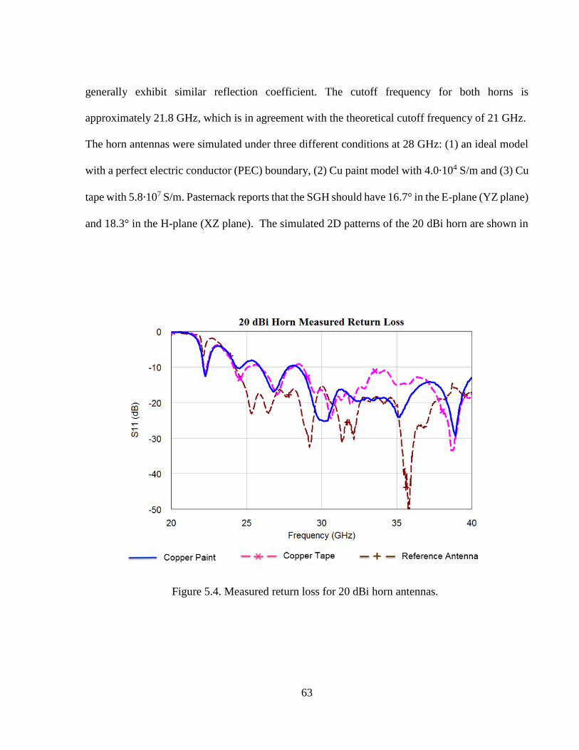
63
generally exhibit similar reflection coefficient. The cutoff frequency for both horns is
approximately 21.8 GHz, which is in agreement with the theoretical cutoff frequency of 21 GHz.
The horn antennas were simulated under three different conditions at 28 GHz: (1) an ideal model
with a perfect electric conductor (PEC) boundary, (2) Cu paint model with 4.0∙104 S/m and (3) Cu
tape with 5.8∙107 S/m. Pasternack reports that the SGH should have 16.7° in the E-plane (YZ plane)
and 18.3° in the H-plane (XZ plane). The simulated 2D patterns of the 20 dBi horn are shown in
Figure 5.4. Measured return loss for 20 dBi horn antennas.

64
Figure 5.5. Figure 5.5(a) simulated 2D patterns of the 3D printed horn with PEC predicts that the
peak gain of the 20 dBi horn will be 19.7 dBi while it is 18.6 dBi for Cu painted antenna and 9.4
dBi for the Cu tape antenna. The 3 dB beam width of the 20 dBi horn with PEC is predicted to be
(a) (b)
(c)
Figure 5.5. Simulated 2D radiation patterns of different cases at 28 GHz: (a) ideal PEC model, (b)
Cu paint 3D printed 20 dBi horn, and (c) Cu tape 3D printed 20 dBi horn.

65
19.7°, while the measured results were 18.5° for Cu paint and 9.4° for Cu tape. The first side lobe
level of the 20 dBi horn with PEC is estimated as 5.4 dBi, while it is 5.5 dBi for Cu paint and 8.5
dBi for Cu tape.
The radiation pattern of the Cu painted horn antenna agrees with that of the ideal PEC. However,
the Cu tape horn antenna has a worse result. The YZ plane cut side lobes are as high as the main
lobe, which makes this implementation less useful. The inside surface of the Cu tape horn has not
been covered with metal which will cause power loss and reflections between the inside ABS
dielectric material of the 3D printed horn.
To measure the radiation patterns of the Ka-band horns, those antennas were connected with a
coaxial-to-waveguide adapter and were placed inside an anechoic chamber. Nearfield System
Inc.’s spherical near-field antenna scanner was used to measure the radiation pattern. The system
(a) (b)
Figure 5.6. Measurement setup for radiation pattern: (a) overview, and (b) AUT test side view.

66
is able to measure up to 26 GHz limited by the long cables max frequency. Shown in Figure 5.6 is
the measurement setup with the NSI scanner.
The radiation patterns of a reference Pasternack SGH, the 3D printed copper paint and copper tape
horns at 26 GHz are shown in Figure 5.7. One can see that the Cu painted 3D printed horn has a
similar radiation pattern compared with the reference while Cu tape horn has increased side lobes.
The YZ cut of Cu tape horn side lobes are as high as the main lobe, which is in agreement with the
previous simulated results. The planar scanner arc covers 200o for the XZ plane and 200o for the
YZ plane. Using the gain comparison method, we calculated the absolute gain of the 3D printed
horn with the reference SGH. With 0.025 mm Cu conductive paint on the 3D printed horn, the
absolute gain is 3.3 dBi. Parameters and results for the three different simulation cases are
summarized in Table 6.2. Based on [62] we set the surface roughness to 40 µm for the Cu tape
antennas in HFSS. The gain is affected more by the ABS material loss than the surface roughness.
The manufactured outside surface roughness after adding Cu paint was estimated using a Gar S-
22 conventional machining microfinish comparator. The surface roughness of the 3D printed Cu
painted horn is estimated to be closer to 6.35 µm, while that for the Cu tape has an even smoother
finish. The manner in which the Cu tape is placed around the horn and the ABS dielectric loss is a
more dominant factor in degrading the antenna gain than the 3D printing surface roughness.
Table 5.2 Summary of simulation and measurement
Parameters Results
Process Roughness
(μm)
Conductivity
(S/m)
Thickness
(μm)
Cutoff Frequency
(GHz)
Simulated 3dB
Beam width
Simulated
Gain (dBi)
Simulated Side
Lobe (dBi)
Ideal model 0 Infinity 0 21.45 (Simulated) 21o 19.7 5.4
Cu paint 6.5 4.0E4 75 21.84 (Measured) 19o 18.6 5.5
Cu tape 40 5.8E7 70 21.78 (Measured) 11o 9.4 8.5
Table 5.3 Summary of simulation and measurement
Parameters Results

67
(a) (b)
(c)
Figure 5.7. Measured 2D radiation patterns of different cases at 26 GHz: (a) Cu paint 3D printed
20 dBi horn, (b) Cu tape 3D printed 20 dBi horn and (c) reference SGH 20 dBi horn.

68
5.6 X-band Antenna 3D model and manufacturing
Figure 5.8 shows the horn antenna designed to work in X-band based on a reference horn sold by
Pasternack (antenna PE9856-15) [64]. The average gain of reference horn is 15 dBi. With respect
to antenna geometry, A (138.7 mm) is the horn length, and B (52.07 mm) and C (71.12 mm) are
the inside aperture dimensions without considering that the dielectric thickness is 1.9 mm, shown
in Table 5.3.
Figure 5.8. Geometry of horn antenna designed in Solidworks.
Table 5.10. Dimensions of X-band horn antenna
Figure 5.51. Geometry of horn antenna designed in Solidworks.
Table 5.11. Dimensions of X-band horn antenna
Type A (mm) B (mm) C (mm) 3D Printed (inner) 138.7 49.5 67.5
Table 5.3. Dimensions of X-band horn antenna
Type A (mm) B (mm) C (mm) 3D Printed (inner) 138.7 49.5 67.5

69
The plastic horns made using the Stratasys machine and were subsequently metallized using
Caswell Cu conductive paint. Three 3-D printed 15 dBi horn antennas were metallized with one
paint layer, two paint layers and three paint layers, respectively. A HUSKY gravity spray gun
shown in Figure 5.10 was used to deposit one layer at each time and dried for three hours. After a
post-fab measurement of the three metallized horn antennas, there was about + 0.1 mm deviation
of the antenna dimensions A, B and C. The conductivity of the Caswell paint is approximately
4.0∙104 S/m, which is 3 orders of magnitude lower than the bulk material [63]. The Cu paint
thickness was measured using a DekTak profilometer, after spraying paint onto a glass slide during
the process. The thickness of one Cu paint layer measured 8 µm. The external surface roughness
after adding Cu paint was estimated using a Gar S-22 conventional machining microfinish
comparator shown in Figure 5.11. The surface roughness of the three 3-D printed Cu painted horns
is estimated to be close to 6 µm. Figure 5.12 shows the photograph of 3D printed 15 dBi horn
Figure 5.9. Stratasys Fortus 400 3D Printing System.

70
antenna with two layers of paint. Other than metal spray copper deposition methods, a 3D printed
horn was sent to a local vendor which provides silver conductive paint metallization. Silver
conductive paint is a commercial metallization process form and can be used in higher frequency
EMI shielding applications where higher surface conductivity is required. The process uses an air
atomizer to spray silver conductive coating onto all surfaces of the ABS 3D printed horn [65]. The
Figure 5.10. HUSKY gravity spray gun
Figure 5.65. HUSKY gravity spray gun
Figure 5.11. S-22 Microfinish Comparator

71
thickness is 5 µm and conductivity is approximately 16.0∙104 S/m. Figure 5.13 shows all four
fabricated 3D printed horn antennas.
Figure 5.12. Photograph of 3D printed 15 dBi horn antenna with two layers of paint: profile view
(A), aperture view (B), and flange view (C).
Figure 5.79. Photograph of 3D printed 15 dBi horn antenna with two layers of paint: profile view
(A), aperture view (B), and flange view (C).
Figure 5.13. Photograph of 3D printed 15 dBi horn antennas: one layer copper paint horn (A), two
layers copper paint horn (B), three layers copper paint horn (C) and sliver paint horn (D).

72
5.7 X-band Horn Simulation and Measurement Results
In order to analyze the performance of the fabricated horn antennas, three different 3-D printed
horn antennas were simulated in the following cases:
A. Antenna model with one layer of paint/metal
B. Antenna model with two layers of paint/metal
C. Antenna model with three layers of paint/metal
A conductive boundary on all the surfaces of the horn antenna was set with a given conductivity,
surface roughness and thickness for each case. The horn antennas’ radiation patterns were
simulated using ANSYS HFSS where the operating frequency was set to 9.5 GHz. The fabricated
horn antennas were connected with a coaxial-to-waveguide adapter and placed inside an anechoic
chamber. Nearfield System Inc.’s planar near-field scanner was used to measure the radiation
pattern. The measurement setup inside an anechoic chamber is shown in Figure 5.14.
Figure 5.14. Measurement setup for radiation pattern.

73
The simulated 2D radiation patterns of the 15 dBi horn are shown in Figure 5.15. Three horns have
a similar peak gain: 15.1 dBi for one layer horn with 8μm thickness, 15.7 dBi for two layers horn
with 16μm thickness and 16.0 dBi for three layers horn with 24μm thickness. The 3 dB beam width
of the horns is predicted to be 29o in simulation. The antenna efficiency for each case is 79.8% for
A, 92.1% for B and 96.6% for C. The simulated paint thickness was increased to 80μm, 160μm
and 240μm. As a result, the radiation patterns did not change, but saturated to 16.2 dBi peak gain,
28.5o beam width and 99.6% efficiency. Based on the simulation results, it is believed that at least
three layers of 24μm thickness paint is required for good radiation performance.
The measured radiation patterns of the three copper paint horns and one silver paint horn are shown
in Figure. 5.16. The planar scanner arc covers 120o for the XZ plane and 100o for the YZ plane.
Using the gain comparison method, the calculated absolute peak gain of the antennas is 13.7 dBi
(a) (b)
Figure 5.15. Simulated 2D radiation patterns at 9.5 GHz: (a) XZ plane and (b) YZ plane.

74
for one layer, 14.1 dBi for two layers, 15.8 dBi for three layers and 15.6 dBi for silver paint at 9.5
GHz. It is believed that the 2 dB lower gain is due to the fact that metal thickness for one layer is
comparable to the surface roughness. Figure 5.17 shows the measured peak gain of the horns from
8.5 GHz to 10.0 GHz. Three layer copper paint varies from 14.9 to 15.8 dB and silver paint varies
from 14.8 to 15.6 dB. Though the silver paint conductivity is 4 times greater than copper paint, the
thinner thickness of the paint may affect the peak gain which causes 0.2 dB lower gain. The two
3D printed horn show a similar performance in general.
(a) (b)
B: Silver Paint Horn C: Three layers Copper Paint Horn
D: Two layers Copper Paint Horn E: One layer Copper Paint Horn
Figure 5.16. Measured 2D radiation patterns at 9.5 GHz: (a) XZ plane, and (b) YZ plane.
Table 5.22. Summary of measurement results

75
Based on the XZ plane patterns, one can see that the Cu painted 3D printed horn antennas have
similar radiation patterns in general and the horn antennas in Case C (three layers of copper paint)
and in Case B (silver paint), have gain closer to the simulated results. In contrast the 3dB beam
width reduced from 24.8o to 21.5o (shown in Table 5.4). This value starts out at 15% lower than
theory (Case A) and reaches up to 30% lower with three layers of Cu pain (Case C), although not
captured in simulation. This can be attributed to the previous bad coaxial cable of the NSI system.
The bad cable caused more variation during the whole measurement. After installing a new cable,
we remeasured three layers and silver paint horns and found that the 3dB beam width is similar
which is in agreement with antenna theory. Based on antenna theory, the 3 dB beam width of the
antenna depends mainly on the shape of the antenna [9]. Comparison of cost and delivery time are
Table 5.4. Summary of measurement results
Parameters Results at 9.5 GHz
Process Roughness
(μm) Conductivity
(S/m) Thickness
(μm) Measured Gain
(dBi) Measured 3dB
Beamwidth
One layer
~6
4.0E4
8 13.7 + 0.2 24.8o
Two layers 16 14.1 + 0.3 23.8o
Three layers 24 15.8 + 0.3 27.5o
Silver Paint by
Cybershield ~5 16.0E4 25 15.6 + 0.2 27.8o

76
summarized in Table 5.5. 3D printed horn with three copper paint metallization provides the lowest
cost and the fastest delivery time.
B: Silver Paint Horn C: Three layers Copper Paint Horn
D: Simulated three layers copper paint horn
Figure 5.17. Measured peak gain over frequency.
Table 5.5. Summary of cost estimates
Process Cost Delivery Time
3D Printed with copper paint
$25 One day
3D Printed with silver paint by Cybershield
$515 2 weeks
Standard Gain Horn $700 2-4 weeks

77
5.8 Conclusion
At Ka-band, 20 dBi horn antennas operating at 28 GHz have been modeled in HFSS simulation,
and fabricated using Stratasys Fortus 400 FDM 3D printing system. Cu conductive paint and Cu
tape have been applied to metalize the 3D printed horns. The measured reflection coefficient was
obtained. According to measurement results, Cu conductive paint has better reflection coefficient
performance. Simulation and measurement results confirm that the Cu painted horn antenna with
three paint layers can generate satisfactory radiation pattern at 28 GHz. However the gain
performance is 70% off compared to a reference standard gain horn. Then at lower frequency, we
investigated the performance of X-band horn antennas were manufactured using FDM 3D printing
and metallized with different conductive paint thickness. The antennas were experimentally
measured in a planar scanner and compared with a standard gain horn to acquire absolute gain.
The simulation and measurement results are in good agreement. Three layers of Cu paint (24mm)
provides the highest gain, which has a value closer to simulated results and similar performance
to commercial metallization process silver painted horns. High and low frequency 3D printed
horns performance, spray deposition method without polishing the surface roughness may not be
a good option for mm-wave printed component metallization. This work confirms that it is feasible
to fabricate millimeter-wave horn antennas using low cost 3D printing with spray deposition
metallization. This effort may provide a cost-effective solution for initial testing without the need
of use military grade horn antennas.

78
CHAPTER 6
SUMMARY AND FUTURE WORK
6.1 Summary
This dissertation has presented efforts on the generation of an approximation higher order Gaussian
beams at E-band using two methods. A physical phase plate combined with a standard gain horn
antenna is a straight forward method and a more compact arrangement of a microstrip patch
antenna array can also be used. After generating OAM modes with both methods, efforts to
demonstrate an OAM-based wireless communication link have been attempted.
This research achieved the following:
Generated approximated HG beams at E-band using physical phase plate and patch array.
Demonstrated that two different OAM beams can be multiplexed and demultiplexed over
the same frequency radio channel at E-band (71-76 GHz) using commercial impulse radios
combined with spiral phase plates at a distance of 2 meters.
Demonstrated at 67 GHz an OAM wireless communication link using circular patch arrays
by generating a twisted EM wave with array and untwisting that wave using a SPP to
measure the RF signal with a spectrum analyzer.
Demonstrated X-band and Ka-band 3D printed horn antennas with Cu paint metallization.
6.2 Future work
To complete the experimental demonstration of a dual-channel at E-band using circular patch
arrays with OAM multiplexing, it would be worthwhile to design a new OAM array 𝑙 = +3 with
12 or 16 elements array. Currently fabricated on FR408 (𝜀𝑟 = 3.75, tan 𝜃 = 0.018), the loss is
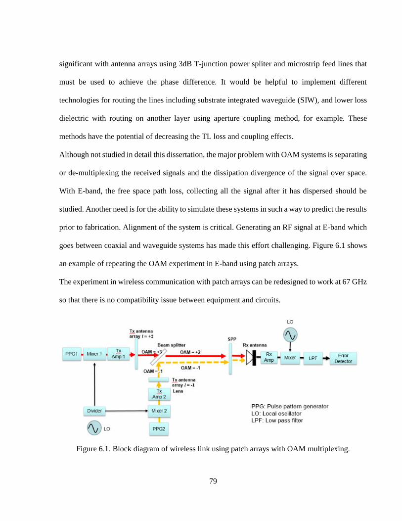
79
significant with antenna arrays using 3dB T-junction power spliter and microstrip feed lines that
must be used to achieve the phase difference. It would be helpful to implement different
technologies for routing the lines including substrate integrated waveguide (SIW), and lower loss
dielectric with routing on another layer using aperture coupling method, for example. These
methods have the potential of decreasing the TL loss and coupling effects.
Although not studied in detail this dissertation, the major problem with OAM systems is separating
or de-multiplexing the received signals and the dissipation divergence of the signal over space.
With E-band, the free space path loss, collecting all the signal after it has dispersed should be
studied. Another need is for the ability to simulate these systems in such a way to predict the results
prior to fabrication. Alignment of the system is critical. Generating an RF signal at E-band which
goes between coaxial and waveguide systems has made this effort challenging. Figure 6.1 shows
an example of repeating the OAM experiment in E-band using patch arrays.
The experiment in wireless communication with patch arrays can be redesigned to work at 67 GHz
so that there is no compatibility issue between equipment and circuits.
Figure 6.1. Block diagram of wireless link using patch arrays with OAM multiplexing.

80
APPENDIX A
COMPARISON GAIN MEASUREMENT USING NSI SCANNING SYSTEM
To make comparison gain measurements, perform the following steps:
1. Perform the near-field or far-field measurement for the Standard Gain Antenna (SGA) (eg.
20 dB gain horn).
2. Transform the data for the SGA to the far-field. In the far field plot setting, click plot
parameters.
Choose comparison method, enter the AUT Max Far-field value shown in the comparison
gain calculation table into the SGA Max Far-field text box. Enter the known SGA gain
into the text box labeled “SGA gain (pre-measured)”. The gain value should be provided
by the manufacturer’s document and at frequency of interest.
Figure A.9. Far-field plot setting in user window of NSI2000 software.

81
3. Replace the SGA with the AUT and do the near-field or far-field measurement under the
same settings (frequency, measure distance, angle...)
4. Transform the data for the AUT to the far-field. In the far-field plot setting, click plot
parameters.
Choose comparison method, plot H-cut or V-cut for the far-field, now the “Calculated AUT
gain” is the gain of the AUT shown in the comparison gain calculation table.
Note: For obtaining gain, measure both SGH and AUT in the same way, either near-field
or far-field.
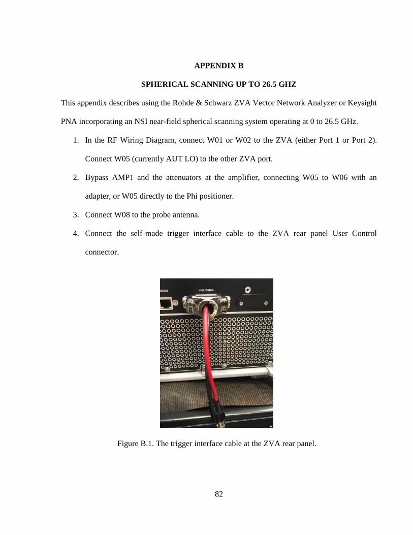
82
APPENDIX B
SPHERICAL SCANNING UP TO 26.5 GHZ
This appendix describes using the Rohde & Schwarz ZVA Vector Network Analyzer or Keysight
PNA incorporating an NSI near-field spherical scanning system operating at 0 to 26.5 GHz.
1. In the RF Wiring Diagram, connect W01 or W02 to the ZVA (either Port 1 or Port 2).
Connect W05 (currently AUT LO) to the other ZVA port.
2. Bypass AMP1 and the attenuators at the amplifier, connecting W05 to W06 with an
adapter, or W05 directly to the Phi positioner.
3. Connect W08 to the probe antenna.
4. Connect the self-made trigger interface cable to the ZVA rear panel User Control
connector.
Figure B.1. The trigger interface cable at the ZVA rear panel.

83
5. Connect the other side interface cable to A05, as shown in the Figure B.2.
6. The LO path through the scanner (using the rotary joints) is used as the RF signal path.
7. Edit the file c:\ c:\NSI2000\dlls\controller.ini. In the [Setup] section at the top, make sure
the following are set:
EnablePNA=0
EnablePnaV9=0 ; 0 = no, 1 = use PNA Instrument, running A.09.xx.xx
firmware
EnableZVA=1 ; 0 = no, 1 = use ZVA Controller
8. Finally set the ZVA to do a normal S21 or S12.
Figure B.2. Control wiring diagram.
Figure B.6.24. Control wiring diagram.

84
Notes:
1. If still using the Keysight PNA to do coaxial measurements below 26.5 GHz. One need use four
connecting metal cables to do the connection at the front panel of PNA as shown in Figure B.3
with all connections to the microwave module tied together. The cables will go directly to the
VNA for S21/S12 measurements.
2. When measuring an AUT, complete the following steps:
1) Measure far-field Hcut of the AUT.
2) Measure far-field Vcut of the AUT.
3) Check the Hcut and Vcut radiation patterns.
4) Complete near-field measurements of the AUT at one operating frequency.
5) Check the near-field measurement results.
6) Complete near-field measurements of the AUT at one frequency list.
Figure B.3. PNA front panel connection.

85
APPENDIX C
OTHER TYPE HORN ANTENNAS
Four pink 3D printed horn antennas (vero material) were fabricated using a Stratasys Connex3 3D
printer, which are shown in Figure C.1. The printing resolution is 0.0006 inches.
The 7GHz 10 dBi 3-D printed horns were metallized with 3 layers of copper paint. Figure C.2
shows the horn connected with a SMA Female input. Far-field H-cut 2D radiation pattern of the
horn is shown in Figure C.3. This reference antenna was used in establishing capability.
Figure C.2. 10 dB WR137 5.85 to 8.2 GHz waveguide 3-D printed copper paint horn with a
SMA Female input using vero material.
Figure C.1. 3-D printed horn antennas using Stratasys Connex 3.
Figure B.6.45. PNA front panel connection.

86
Figure C.4 shows three 10 dB Ka-band horns. The CNC milling horn (b) was fabricated at
Protolab with Aluminium, that cost $161.87. Return loss comparison of those horns is shown in
Figure C.5 and far-field H-cut radiation patterns comparison is shown in Figure C.6.
(a) (b) (c)
Figure C.4. 10 dB Ka-band Horns: (a) 3-D printed copper paint horn, (b) CNC Milling horn and
(c) Pasternack standard gain horn with waveguide to coax adapter.
Figure C.3. Far-field H-cut radiation pattern of 10 dB WR137 3-D printed copper paint horn at
6.5 GHz.
Figure B.6.59. PNA front panel connection.

87
Figure C.5. 10 dB Ka-band Horn Return Loss Comparison.
Figure B.6.73. PNA front panel connection.
Figure C.6. Far-field H-cut radiation patterns comparison.

88
REFERENCES
[1] Y. G. Li and G. L. Stuber, Orthogonal frequency division multiplexing for wireless
communications. Springer Science & Business Media, 2006.
[2] J. D. Park, S. Kang, S. V. Thyagarajan, E. Alon, and A. M. Niknejad, “A 260 GHz fully
integrated CMOS transceiver for wireless chip-to-chip communication,” IEEE Symp. VLSI
Circuits, Dig. Tech. Pap., vol. 2, pp. 48–49, 2012.
[3] F. Tamburini, B. Thidé, E. Mari, A. Sponselli, A. Bianchini, and F. Romanato,
“‘Encoding many channels on the same frequency through radio vorticity: First
experimental test,’” New J. Phys., vol. 14, 2012.
[4] F. Tamburini, E. Mari, A. Sponselli, B. Thidé, A. Bianchini, and F. Romanato, “Encoding
many channels on the same frequency through radio vorticity: first experimental test,”
New J. Phys., vol. 14, no. 3, p. 33001, 2012.
[5] Y. Yan et al., “High-capacity millimetre-wave communications with orbital angular
momentum multiplexing,” Nat. Commun., vol. 5, pp. 1–9, 2014.
[6] H. Yao et al., “Patch antenna array for the generation of millimeter-wave Hermite–
Gaussian beams,” IEEE Antennas Wirel. Propag. Lett., vol. 15, pp. 1947–1950, 2016.
[7] H. Huang et al., “100 Tbit/s free-space data link enabled by three-dimensional
multiplexing of orbital angular momentum, polarization, and wavelength,” Opt. Lett., vol.
39, no. 2, pp. 197–200, 2014.
[8] J. Wang et al., “N-dimentional multiplexing link with 1.036-Pbit/s transmission capacity
and 112.6-bit/s/Hz spectral efficiency using OFDM-8QAM signals over 368 WDM pol-
muxed 26 OAM modes,” in Optical Communication (ECOC), 2014 European Conference
on, 2014, pp. 1–3.
[9] A. E. Willner et al., “Recent advances in high-capacity free-space optical and radio-
frequency communications using orbital angular momentum multiplexing,” Philos. Trans.
R. Soc. A Math. Phys. Eng. Sci., vol. 375, no. 2087, p. 20150439, 2017.
[10] E. Communications. LLC, “70/80 GHz Overview,” 2016. [Online]. Available:
https://www.e-band.com/70-80-GHz-Overview. [Accessed: 10-Jan-2017].
[11] S. Orazio, Principles of lasers. Springer, New York, 2010.
[12] B. E. A. Saleh, M. C. Teich, and B. E. Saleh, Fundamentals of photonics, vol. 22. Wiley
New York, 1991.
89
[13] E. J. Galvez, “Gaussian beams in the optics course,” Am. J. Phys., vol. 74, no. 4, pp. 355–
361, 2006.
[14] Wikipedia, “Gaussian beams.” [Online]. Available:
https://en.wikipedia.org/wiki/Gaussian_beam. [Accessed: 10-Jan-2017].
[15] E. G. Abramochkin and V. G. Volostnikov, “Generalized gaussian beams,” J. Opt. A Pure
Appl. Opt., vol. 6, no. 5, p. S157, 2004.
[16] M. W. Beijersbergen, L. Allen, H. Van der Veen, and J. P. Woerdman, “Astigmatic laser
mode converters and transfer of orbital angular momentum,” Opt. Commun., vol. 96, no.
1–3, pp. 123–132, 1993.
[17] J. Janousek et al., “Optical entanglement of co-propagating modes,” Nat. Photonics, vol.
3, no. 7, p. 399, 2009.
[18] Wikipedia, “Hermite polynomials.” [Online]. Available:
https://en.wikipedia.org/wiki/Hermite_polynomials. [Accessed: 10-Jan-2017].
[19] G. E. Andrews, R. Askey, and R. Roy, Special Functions Cambridge University Press.
1999.
[20] Wikipedia, “Laguerre polynomials.” [Online]. Available:
https://en.wikipedia.org/wiki/Laguerre_polynomials#Generalized_Laguerre_polynomials.
[Accessed: 17-Jan-2017].
[21] G. A. Turnbull, D. A. Robertson, G. M. Smith, L. Allen, and M. J. Padgett, “The
generation of free-space Laguerre-Gaussian modes at millimetre-wave frequencies by use
of a spiral phaseplate,” Opt. Commun., vol. 127, no. 4–6, pp. 183–188, 1996.
[22] S. Sharma, H. Yao, R. Henderson, S. Ashrafi, and D. Macfarlane, “Predictive Method for
Analyzing OAM at Radio Frequencies,” in Proceedings of the 2017 Texas Symposium on
Wireless and Microwave Circuits and Systems, WMCS 2017, 2017, pp. 3–6.
[23] A. Nicolas, L. Veissier, E. Giacobino, D. Maxein, and J. Laurat, “Quantum state
tomography of orbital angular momentum photonic qubits via a projection-based
technique,” New J. Phys., vol. 17, pp. 1–16, 2015.
[24] E. J. Galvez, Gaussian beams. Colgate University, 2009.
[25] J. D. Jackson, Classical Electrodynamics. John Wiley & Sons, 1999.
[26] L. Allen, M. W. Beijersbergen, R. J. C. Spreeuw, and J. P. Woerdman, “Orbital angular
momentum of light and the transformation of Laguerre-Gaussian laser modes,” Phys. Rev.
A, vol. 45, no. 11, pp. 8185–8189, 1992.

90
[27] Y. Zhao, J. S. Edgar, G. D. M. Jeffries, D. McGloin, and D. T. Chiu, “Spin-to-orbital
angular momentum conversion in a strongly focused optical beam,” Phys. Rev. Lett., vol.
99, no. 7, pp. 15–18, 2007.
[28] A. Bennis, R. Niemiec, C. Brousseau, K. Mahdjoubi, and O. Emile, “Flat plate for OAM
generation in the millimeter band,” in Antennas and Propagation (EuCAP), 2013 7th
European Conference on, 2013, pp. 3203–3207.
[29] A. Tennant, Q. Bai, and B. Allen, “Experimental circular phased array for generating
OAM radio beams,” Electron. Lett., vol. 50, no. 20, pp. 1414–1415, 2014.
[30] J. Wang et al., “Terabit free-space data transmission employing orbital angular
momentum multiplexing,” Nat. Photonics, vol. 6, no. 7, pp. 488–496, 2012.
[31] Z. Li, Y. Ohashi, and K. Kasai, “A dual-channel wireless communication system by
multiplexing twisted radio wave,” Eur. Microw. Week 2014 Connect. Futur. EuMW 2014
- Conf. Proceedings; EuMC 2014 44th Eur. Microw. Conf., pp. 235–238, 2014.
[32] F. Spinello et al., “Experimental near field OAM-based communication with circular
patch array,” physics.optics, pp. 1–10, 2015.
[33] Y. Ren et al., “Experimental demonstration of 16 Gbit/s millimeter-wave communications
using MIMO processing of 2 OAM modes on each of two transmitter/receiver antenna
apertures,” in Global Communications Conference (GLOBECOM), 2014 IEEE, 2014, pp.
3821–3826.
[34] Z. Zhao et al., “A dual-channel 60 GHz communications link using patch antenna arrays
to generate data-carrying orbital-angular-momentum beams,” 2016 IEEE Int. Conf.
Commun. ICC 2016, 2016.
[35] H. Yao et al., “Experimental demonstration of a dual-channel E-band communication link
using commercial impulse radios with orbital angular momentum multiplexing,” IEEE
Radio Wirel. Symp. RWS, pp. 51–54, 2017.
[36] D. R. Tompkins Jr and P. F. Rodney, “Six-parameter Gaussian modes in free space,”
Phys. Rev. A, vol. 12, no. 2, p. 599, 1975.
[37] H. Yao et al., “Patch antenna array for the generation of millimeter-wave hermite-
Gaussian beams,” IEEE Antennas Wirel. Propag. Lett., vol. 15, no. c, pp. 1947–1950,
2016.
[38] B. Ndagano, N. Mphuthi, G. Milione, and A. Forbes, “Comparing mode-crosstalk and
mode-dependent loss of laterally displaced orbital angular momentum and Hermite–
Gaussian modes for free-space optical communication,” Opt. Lett., vol. 42, no. 20, p.
4175, Oct. 2017.

91
[39] S. Gregson, J. McCormick, D. J. van Rensburg, and C. Parini, Theory and practice of
modern antenna range measurements. The Institution of Engineering and Technology,
2014.
[40] C. A. Balanis, Antenna Theory. John Wiley & Sons, 1982.
[41] W. L. Stutzman and G. A. Thiele, Antenna theory and design. John Wiley & Sons, 2012.
[42] “Rectangular Microstrip Antenna,” antenna-theroy.com. [Online]. Available:
http://www.antenna-theory.com/antennas/patches/antenna.php. [Accessed: 20-Jan-2016].
[43] L. I. Basilio, M. A. Khayat, J. T. Williams, and S. A. Long, “The dependence of the input
impedance on feed position of probe and microstrip line-fed patch antennas,” IEEE Trans.
Antennas Propag., vol. 49, no. 1, pp. 45–47, 2001.
[44] S. R. Aroor, “System-on-package integration for millimeter-wave circuits using low-cost
laminates,” PhD dissertation, The University of Texas at Dallas, 2013.
[45] H. Hayashi, Y. Nakasha, M. Aota, and N. Sato, “Millimeter-wave impulse radio
technology,” Fujitsu Sci. Tech. J, vol. 49, no. 3, pp. 350–355, 2013.
[46] V. S. Inc, “JDSU MTS-6000 Compact Test Platform,” 2016. [Online]. Available:
https://www.viavisolutions.com/en-uk/products/t-berd-mts-6000a-compact-network-test-
platform. [Accessed: 10-Jan-2016].
[47] A. M. Gretarsson, “Basic paraxial optics toolkit,” 2007. [Online]. Available:
https://www.mathworks.com/matlabcentral/fileexchange/15459-basic-paraxial-optics-
toolkit?focused=5091293&tab=function&s_tid=gn_loc_drop. [Accessed: 10-Jan-2017].
[48] A. E. Siegman, Lasers. University Science Books, 1986.
[49] Z. Zhao et al., “Experimental demonstration of 16-Gbit/s millimeter-wave
communications link using thin metamaterial plates to generate data-carrying orbital-
angular-momentum beams,” in Communications (ICC), 2015 IEEE International
Conference on, 2015, pp. 1392–1397.
[50] S. M. Mohammadi et al., “Orbital angular momentum in radio—a system study,” IEEE
Trans. Antennas Propag., vol. 58, no. 2, pp. 565–572, 2010.
[51] L. Fang, H. Yao, and R. M. Henderson, “OAM antenna arrays at E-band,” IEEE MTT-S
Int. Microw. Symp. Dig., pp. 658–661, 2017.
[52] F. C. Commission, “Use of spectrum bands above 24 GHz for mobile radio services,” Fed
Regist, vol. 81, no. 164, pp. 58270–58308, 2016.
[53] M. D’Auria et al., “3-D printed metal-pipe rectangular waveguides,” IEEE Trans.
92
Components, Packag. Manuf. Technol., vol. 5, no. 9, pp. 1339–1349, 2015.
[54] B. Zhang, P. Linnér, C. Karnfelt, P. L. Tarn, U. Södervall, and H. Zirath, “Attempt of the
metallic 3D printing technology for millimeter-wave antenna implementations,” in
Microwave Conference (APMC), 2015 Asia-Pacific, 2015, vol. 2, pp. 1–3.
[55] B. Liu, X. Gong, and W. J. Chappell, “Applications of layer-by-layer polymer
stereolithography for three-dimensional high-frequency components,” IEEE Trans.
Microw. Theory Tech., vol. 52, no. 11, pp. 2567–2575, 2004.
[56] B. Mueller, “Additive manufacturing technologies–Rapid prototyping to direct digital
manufacturing,” Assem. Autom., vol. 32, no. 2, 2012.
[57] E. Decrossas, T. Reck, C. Lee, C. Jung-Kubiak, I. Mehdi, and G. Chattopadhyay,
“Evaluation of 3D printing technology for corrugated horn antenna manufacturing,” in
Electromagnetic Compatibility (EMC), 2016 IEEE International Symposium on, 2016, pp.
251–255.
[58] Y. Konishi, T. Nishino, H. Yukawa, and Y. Aramaki, “Millimeter-wave plastic waveguide
phased array antenna,” in Antennas and Propagation Society International Symposium
(APSURSI), 2010 IEEE, 2010, pp. 1–4.
[59] “High performace horn antenna design.” [Online]. Available:
http://www.radio.feec.vutbr.cz/kosy/soubory/bocia/High_performance_horn_antenna_desi
gn_II.pdf. [Accessed: 20-Feb-2017].
[60] I. Pasternack Enterprises, “WR-28 Standard Gain Horn Antenna Operating From 26.5
GHz to 40.0 GHz With a Nominal 20 dBi Gain.” [Online]. Available:
https://www.pasternack.com/wr-28-26.5-ghz-to-40.0-ghz-standard-gain-horns-
category.aspx. [Accessed: 20-Feb-2017].
[61] I. San Diego Plasticis, “ABS Acrylonitrile Butadiene Styrene.” [Online]. Available:
http://www.sdplastics.com/abs.html. [Accessed: 20-Feb-2017].
[62] C. R. Garcia, R. C. Rumpf, H. H. Tsang, and J. H. Barton, “Effects of extreme surface
roughness on 3D printed horn antenna,” Electron. Lett., vol. 49, no. 12, pp. 734–736,
2013.
[63] Casewell Inc., “Copper Conductive Paint.” [Online]. Available:
http://www.caswellplating.com/copper-conductivity. [Accessed: 20-Feb-2017].
[64] I. Pasternack Enterprises, “WR-90 Standard Gain Horn Antenna Operating From 8.2 GHz
to 12.4 GHz With a Nominal 15 dBi Gain.” [Online]. Available:
https://www.pasternack.com/standard-gain-horn-waveguide-size-wr90-pe9856-15-P.aspx.
[Accessed: 20-Jun-2017].

93
[65] I. Cybershield, “Conductive Sheilding Paint Application.” [Online]. Available:
https://www.cybershieldinc.com/conductive-shielding-paint/. [Accessed: 20-Jun-2017].

94
BIOGRAPHICAL SKETCH
Haohan Yao was born in Chongqing, China. He received the B.S. degree in Electronic Science
and Technology from Zhengzhou University, Zhengzhou, China, in 2010 and the M.S. degree in
computer engineering from Boston University in 2012. He is currently a member of IEEE. His
research interests include millimeter-wave design, simulation and characterization of high order
Gaussian beams and antennas for wireless communication. He has a wife, Jingshuang and one
child, Dilan.

CURRICULUM VITAE
Haohan Yao
SKILLS
* Solid knowledge of antenna fundamental and radiation theory.
* Proficient in Electromagnetic Simulation tools (ANSYS HFSS, FEKO, and CST MICROWAVE STUDIO).
* Proficient in Keysight ADS, NI AWR Microwave Office and Cadence Spectre RF circuit design.
* Proficient in RF test equipment (Keysight and R&S vector network analyzer, Keysight spectrum analyzer, RF signal
generator and signaling testers) and NSI near-field scanner system (planar and spherical scanners) in the anechoic
chamber.
* Proficient in Altium Designer and PCB board design.
* Proficient in MATLAB scripting for data collection and analysis.
* Proficient with nano fabrication, standard photolithography and etching process.
* Familiar with waveguide to coaxial transition RF probe.
* Familiar with Solidworks and Stratasys 3D printing mechanical design.
EDUCATION
* The University of Texas at Dallas, Richardson, TX Aug 2013 – Present
PhD, Electrical Engineering GPA: 3.83 / 4.0
Thesis: “Radio Frequency Communication using Higher Order Gaussian beams”
Advisor: Dr. Rashaunda Henderson
* Boston University College of Engineering, Boston, MA Aug 2010 – May 2012
Master of Science, Computer Engineering GPA: 3.78 / 4.0
* Zhengzhou University College of Physical Engineering, Zhengzhou, China Sep 2006 – June 2010
Bachelor of Science, Electronic Science and Technology GPA: 3.30 / 4.0
Awarded scholarship for excellent student in Zhengzhou University for 2006-07, 2007-08, and 2008-09 academic years
INDUSTRY EXPERIENCE
* UTD, Texas Analog Center of Excellence (TxACE) Research Assistant May 2014 to Present
Research on new technologies for 5G wireless, increasing channel capacity with mode division multiplexing
of EM beams using orbital angular momentum (OAM) or Hermite-Gaussian (HG) waves at E-band.
Completed photolithography, etching and evaporation training. Manufactured interconnects for a transceiver
chip, E-band (71-76 GHz) millimeter wave patch arrays at Natural Science and Engineering Research
Laboratory (NSERL).

* IBM, Chongqing, China Client representative June 2012 to Dec 2012
Called on qualified lists of clients. Understood the client environments to detect projects and advise them on
IBM's best solutions. Completed training from IBM Smart Career and IBM Global Sales School (GSS).
RF/ANTENNNA DESIGN EXPERIENCE
*OAM beams communication at E-band (71-76 GHz) using commercial point-to-point
radio
Designed and fabricated two Spiral Phase Plates (SPP) to generate two different OAM beams at E-band.
Measured those two OAM beams far field pattern using NSI scanner system in the anechoic chamber.
Experimentally demonstrated two OAM beams multiplexing and demultiplexing in a free-space communication
link on the same frequency channel which finally doubled the channel capacity.
* Designing patch antenna arrays operating at E-band (71-76 GHz)
Designed and fabricated patch antenna arrays to generate millimeter-wave Hermite-Gaussian beams and
Laguerre-Gaussian beams at E-band.
Placed the antenna arrays inside an anechoic chamber and measured reflection coefficients and radiation
pattern using NSI spherical scanner system incorporating a Keysight microwave vector network analyzer
(VNA).
* Designing X-band (8 - 12 GHz) and Ka-band (26.5 - 40 GHz) 3D printed horn antennas
Designed and fabricated X-band and Ka-band pyramidal horn antennas using Stratasys 3D printer with
acrylonitrile butadiene styrene (ABS) material.
Sprayed copper conductive or sliver conductive paint inside and outside of the antennas.
Measured reflection coefficients and placed the antennas inside an anechoic chamber. Measured radiation
pattern using NSI spherical scanner system incorporating a Keysight VNA.
* Physical phase plate for the generation of a millimeter-wave Hermite-Gaussian beam
Designed and fabricated a physical phase plate to generate millimeter-wave Hermite-Gaussian beams at E-
band.
Measured the HG beam far field pattern using NSI scanner system in the anechoic chamber.
* Microwave design and measurement lab
Designed, fabricated and measured the following passive RF circuits: resonators, filters, Wilkinson power
divider and quadrature hybrid coupler up to 8 GHz.
Hands on experience on circuit schematics, layout, EM simulation using AWR Microwave Office and AXIEM
EM simulator, milling on FR-4 and Duroid boards and soldering.
Completed RF measurements (10 MHz to 8 GHz) for all the boards.
PUBULICATIONS/CONFERENCE PAPERS
1. H. Yao, L. Fang, R. Henderson, “Evaluating conductive paint performance on 3-D printed horn antennas,” IEEE
Radio and Wireless Symposium (RWS), pp. 191-193, 2018.
2. H. Yao, H. Kuma, T. Ei, S. Sharma, R. Henderson, S. Ashrafi, D. L. MacFarlane, Z. Zhao, Y. Yan, A. Willner,
“Experimental demonstration of a dual-channel E-band communication link using commercial impulse radios with
orbital angular momentum multiplexing,” IEEE Radio and Wireless Symposium (RWS), pp. 51-54, 2017.
3. H. Yao, S. Sharma, R. Henderson, S. Ashrafi, D. L. MacFarlane, “Ka band 3D printed horn antenna,” in

proceedings of 2017 Texas Symposium on Wireless and Microwave Circuits and Systems, WMCS 2017, no.mm,
pp.17-20, 2017.
4. H. Yao, H. Kuma, T. Ei, N. Ashrafi, T. LaFave, S. Ashrafi, D. L. MacFarlane, R. Henderson, “Patch antenna array
for the generation of millimeter-wave Hermite-Gaussian beams,” IEEE Antennas and Wireless Propagation Letters,
vol.15, no.99, pp.1947-1950, 2016.
5. L. Fang, H. Yao, R. Henderson, “Design and Performance of OAM Modes Generated using Dipole Arrays with
Different Feeds,” IEEE Radio and Wireless Symposium (RWS), pp. 200-202, 2018.
6. L. Fang, H. Yao, R. Henderson, “OAM antenna arrays at E-band,” IEEE International Microwave Symposium (IMS),
pp. 658-661, 2017.
7. S. Sharma, H. Yao, R. Henderson, S. Ashrafi, D. L. MacFarlane, “Predictive method for multiplexing Laguerre-
Gaussian beams at radio frequencies,” in proceedings of 2017 Texas Symposium on Wireless and Microwave
Circuits and Systems, WMCS 2017, no.mm, pp.1-4, 2017.
8. H. Kumar, H. Yao, T. Ei, N. Ashrafi, T. LaFave, S. Ashrafi, D. L. MacFarlane, R. Henderson, “Physical phase plate
for the generation of a millimeter-wave Hermite-Gaussian beam,” IEEE Radio and Wireless Symposium (RWS),
pp. 234-237, 2016.
PRESENTATIONS
1. L. Fang, H. Yao, “OAM antenna arrays at E-band,” presented, IEEE International Microwave Symposium (IMS), June 2017.
2. H. Yao, “Ka band 3D printed horn antennas,” presented, 2017 Texas Symposium on Wireless and Microwave Circuits and Systems, March 2017.
3. H. Yao, “Experimental demonstration of a dual-channel E-band communication link using commercial impulse radios with orbital angular momentum multiplexing.” presented, TxACE Weekly Lunch Meeting, Feb 2017.
4. H. Yao, “Experimental demonstration of a dual-channel E-band communication link using commercial impulse radios with orbital angular momentum multiplexing,” presented, 2017 IEEE Radio and Wireless Symposium (RWS), Jan 2017.
5. H. Yao, “Experimental demonstration of a dual-channel E-band communication link using commercial impulse radios with orbital angular momentum multiplexing,” presented, 2016 Annual TxACE Symposium, October 2016.
6. H. Yao, “Spiral phase plates for the generation of millimeter-wave Laguerre-Gaussian beams.” presented, IEEE MTT Texas Symposium on Wireless and Microwave Circuits and Systems, March 2016.
7. H. Yao, “Generating millimeter-wave Hermite-Gaussian beams at E-band.” presented, TxACE Weekly Lunch Meeting, Feb 2016.
8. H. Kumar, H. Yao, “Physical phase plate for the generation of a millimeter-wave Hermite-Gaussian beam,” presented, 2016 IEEE Radio and Wireless Symposium (RWS), Jan 2016.
9. H. Yao, “Patch antenna array for the generation of millimeter-wave Hermite-Gaussian beams,” presented, 2015 Annual TxACE Symposium, October 2015.
TEACHING
* Graduate Teaching Assistant EERF 7V89 Active Microwave Circuit Design, fall 2017.
* Graduate Teaching Assistant EERF 6396 Microwave Design Measurement, spring 2017.
* Graduate Teaching Assistant for EERF 6311 RF and Microwave Circuits, fall 2016 and spring 2017.
* Undergraduate Teaching Assistant for EE 4368 RF Circuits Design Principles, fall 2016.
Delivered lectures on experimental procedure and problem sessions, supervised experiments, graded homework and lab reports, and held office hours.
Course Description
* EERF 7V89 Active Microwave Circuit Design: This lecture and lab course covers design of linear and non-linear
microwave active circuits, including component characterization, biasing, linear and non-linear analysis.

* EERF6396 Microwave Design Measurement: This lecture and lab course covers the fundamentals of microwave
component design and measurements, including vector impedance (scattering parameters), scalar measurements and spectrum analysis.
* EERF6311 RF and Microwave Circuits: Analysis and design of RF and microwave circuits.
* EE 4368 RF Circuits Design Principles: Principles of high-frequency design, transmission lines, the Smith chart,
impedance matching using both lumped and distributed components, and simple amplifier design.
PROFESSIONAL MEMBERSHIP
* Student member of IEEE