Embed Size (px)
Citation preview
Radio Frequency Effects on the Clock Networksof Digital Circuits
Hongxia Wang, Cagdas Dirik, Samuel V. Rodriguez, Amol V. Gole* and Bruce JacobDepartment of Electrical and Computer EngineeringUniversity of Maryland, College Park, MD 20742{hwang, cdirik, samvr, amol, blj}@eng.umd.edu
http://www.ece.umd.edu/~blj/integrity/
Abstract — Radio frequency interference (RFI) can haveadverse effects on commercial electronics. Current properties ofhigh performance integrated circuits (ICs), such as very smallfeature sizes, high clock frequencies, and reduced voltage levels,increase the susceptibility of these circuits to RFI, causing themto be more prone to smaller interference levels. Also, recentdevelopments of mobile devices and wireless networks create ahostile electromagnetic environment for ICs. Therefore, it isimportant to measure the susceptibility of ICs to RFI. In thisstudy, we investigate the susceptibility levels to RFI of the clocknetwork of a basic digital building block. Our experimental setupis designed to couple a pulse modulated RF signal using the pindirect injection method. The device under test is an 8-bit ripplecounter, designed and fabricated using AMI 0.5 µm processtechnology. Our experiments showed that relatively low levels ofRFI (e.g., 16.8 dBm with carrier frequency of 1 GHz) couldadversely affect the normal functioning of the device under test.
Keywords: RFI, Pin direct injection method, Power reflectioncoefficient, Pulsed modulated RF, Clock network
I. INTRODUCTION
Current high performance integrated circuits (ICs), such asmicroprocessors, have very small feature sizes (e.g., 0.13 µm)and are clocked at frequencies well into the GHz range whileoperating at reduced voltage levels (e.g., 1.5 V). Although thishas improved the ability and performance of modern systems,it has also increased their susceptibility to radio frequencyinterference (RFI). The electrical charge required in transistorswitching decreases with relatively smaller IC feature sizes.Correspondingly, the energy required to disturb the switchingprocess is reduced, making it easier to disturb the circuit withlower RFI signal levels. As the switching speed of the ICsincreases and the supply voltage scales down, the noise marginalso becomes smaller. This allows external disturbances, suchas those induced by RFI, to degrade the signal integrity.Consequently, the electronic systems that are integrated with
*Amol Gole is currently a patent examiner of CAIPAU, US Patent andTrademark Office, Arlington, VA. Email: [email protected]
these high performance chips are more prone to be affected bylower RFI levels.
Numerous structures in a computer system (e.g., externalwires, cables, PCB traces, bonding interconnects, internal metalchip signals like power, ground, and data lines) can act asantennae in the presence of RFI, which is either radiated frompowerful radio transmitters, wireless network devices, mobilephones and PDAs, or intentionally generated for maliciousreasons. These unintentional antennae can serve to couple RFnoise into the core circuit [1, 2, 3]. RFI that is coupled by thesystem can induce unwanted currents, which cause variousdisturbances. The inherent non-linear behavior of electronicdevices in digital circuits can also cause RF signal rectificationand amplification and is said to be the primary upsetmechanism for integrated circuits under RFI [4]. Also, inter-modulation, cross-modulation and other disturbances areimmediate effects of interference [5]. These unwantedinterferences, when interpreted as or superimposed on systemsignals, can cause spurious state changes on logic devices andsystem-level breakdown [3, 4].
The power levels and frequency range for which circuits aremore susceptible to RFI have been studied recently. Previousstudies observed changes on the I-V characteristics of diodes,BJTs, and MOSFETs under RFI [1]. Susceptibility levels of amicrocontroller and a DSP chip have been measured for RFinterference up to 400 MHz, and data corruption was observedon the communication path between the microcontroller andRAM memory [2]. The same study showed that 20 dBm RFinterferences at 350 MHz were enough to trigger the reset pinof a voltage regulator. Another study investigated the effects ofRF interference on the input ports of a 0.7 µm CMOS inverterwith frequencies in the 20 MHz – 1 GHz ranges and powerlevels up to 15 dBm [3]. Dynamic failures in the form ofvariations in input pad propagation delay and static failureswere observed when pad output signals were misinterpreted asthey strayed beyond the high and low voltage logic thresholds.Hence, there is a growing concern over the electromagneticcompatibility of ICs in hostile RFI environments and wider RFfrequency ranges, such as those at and above 1 GHz. To thisend, power levels and frequency ranges of RFI to which high
Copyright © 2004 IEEE. Published in the Proceedings of the 2004 IEEE International Symposium on Electromagnetic Compatibility, August 9-13, 2004 in Santa Clara,CA. Personal use of this material is permitted. However, permission to reprint/republish this material for advertising or promotional purposes or for creating newcollective works for resale or redistribution to servers or lists, or to reuse any copyrighted component of this work in other works, must be obtained from the IEEE.Contact: Manager, Copyrights and Permissions / IEEE Service Center /445 Hoes Lane / P.O. Box 1331 / Piscataway, NJ 08855-1331, USA.
Tel: + Intl. 908-562-3966.
speed ICs are more sensitive, have been studied in this paper.Also, the input characteristics of the circuit, such as inputimpedance, are being investigated.
This work follows a system-level approach to quantify andgeneralize the susceptibility levels of digital ICs. On thesystem-level, signals in the basic blocks of memory and CPUare mainly composed of the clock, power-ground, and datanetworks. These signals are interpreted differently undernormal operation. The timing and voltage levels of the datainput/output signals are important, whereas for clock signals,the timing of low-to-high or high-to-low transitions is mostcritical. Any level shifts on power/ground planes can also causemalfunctioning of the circuit. In this study, we focused onmeasuring the susceptibility levels of the clock network. Oursusceptibility test bench is designed to couple pulse-modulatedRF signals on the clock network using the pin direct injectionmethod to have better control of the power level that is appliedto the device under test (DUT).
II. EXPERIMENTAL SETUP AND MEASUREMENT
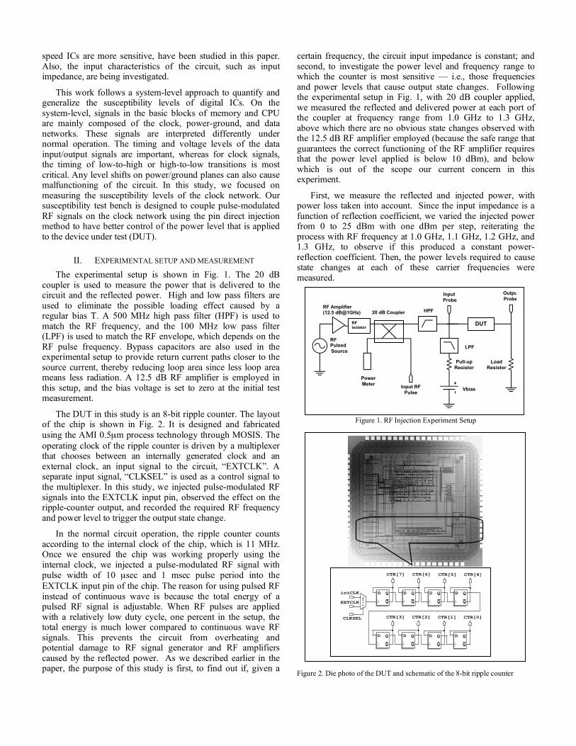
The experimental setup is shown in Fig. 1. The 20 dBcoupler is used to measure the power that is delivered to thecircuit and the reflected power. High and low pass filters areused to eliminate the possible loading effect caused by aregular bias T. A 500 MHz high pass filter (HPF) is used tomatch the RF frequency, and the 100 MHz low pass filter(LPF) is used to match the RF envelope, which depends on theRF pulse frequency. Bypass capacitors are also used in theexperimental setup to provide return current paths closer to thesource current, thereby reducing loop area since less loop areameans less radiation. A 12.5 dB RF amplifier is employed inthis setup, and the bias voltage is set to zero at the initial testmeasurement.
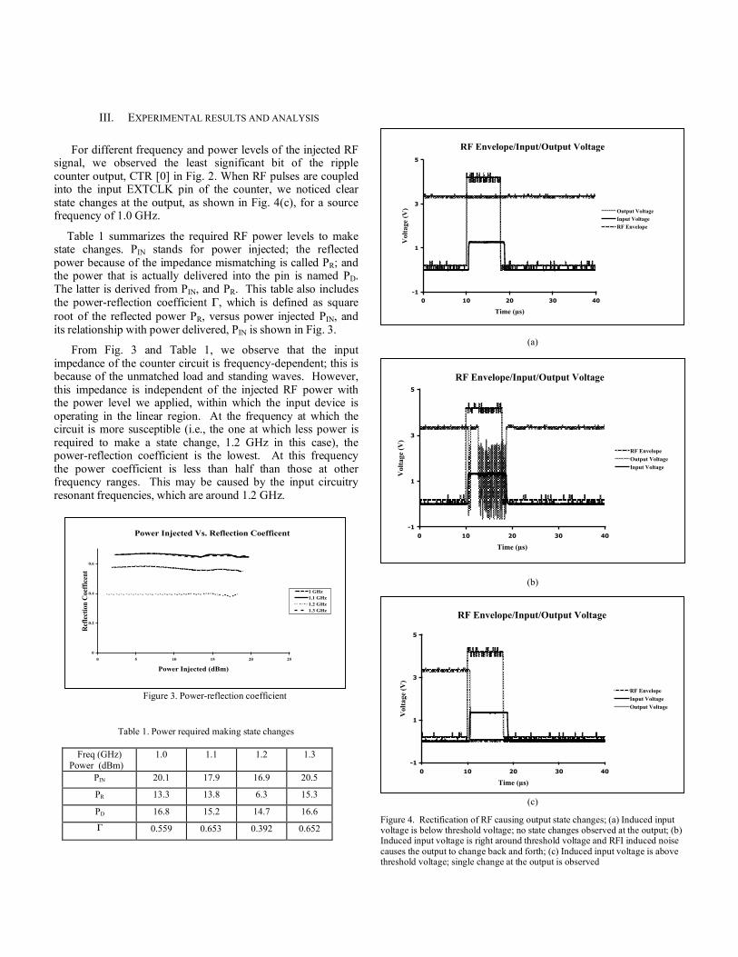
The DUT in this study is an 8-bit ripple counter. The layoutof the chip is shown in Fig. 2. It is designed and fabricatedusing the AMI 0.5µm process technology through MOSIS. Theoperating clock of the ripple counter is driven by a multiplexerthat chooses between an internally generated clock and anexternal clock, an input signal to the circuit, “EXTCLK”. Aseparate input signal, “CLKSEL” is used as a control signal tothe multiplexer. In this study, we injected pulse-modulated RFsignals into the EXTCLK input pin, observed the effect on theripple-counter output, and recorded the required RF frequencyand power level to trigger the output state change.
In the normal circuit operation, the ripple counter countsaccording to the internal clock of the chip, which is 11 MHz.Once we ensured the chip was working properly using theinternal clock, we injected a pulse-modulated RF signal withpulse width of 10 µsec and 1 msec pulse period into theEXTCLK input pin of the chip. The reason for using pulsed RFinstead of continuous wave is because the total energy of apulsed RF signal is adjustable. When RF pulses are appliedwith a relatively low duty cycle, one percent in the setup, thetotal energy is much lower compared to continuous wave RFsignals. This prevents the circuit from overheating andpotential damage to RF signal generator and RF amplifierscaused by the reflected power. As we described earlier in thepaper, the purpose of this study is first, to find out if, given a
certain frequency, the circuit input impedance is constant; andsecond, to investigate the power level and frequency range towhich the counter is most sensitive — i.e., those frequenciesand power levels that cause output state changes. Followingthe experimental setup in Fig. 1, with 20 dB coupler applied,we measured the reflected and delivered power at each port ofthe coupler at frequency range from 1.0 GHz to 1.3 GHz,above which there are no obvious state changes observed withthe 12.5 dB RF amplifier employed (because the safe range thatguarantees the correct functioning of the RF amplifier requiresthat the power level applied is below 10 dBm), and belowwhich is out of the scope our current concern in thisexperiment.
First, we measure the reflected and injected power, withpower loss taken into account. Since the input impedance is afunction of reflection coefficient, we varied the injected powerfrom 0 to 25 dBm with one dBm per step, reiterating theprocess with RF frequency at 1.0 GHz, 1.1 GHz, 1.2 GHz, and1.3 GHz, to observe if this produced a constant power-reflection coefficient. Then, the power levels required to causestate changes at each of these carrier frequencies weremeasured.
Figure 1. RF Injection Experiment Setup
Figure 2. Die photo of the DUT and schematic of the 8-bit ripple counter
D Q
Q
CTR[4]
D Q
Q
CTR[5]
D Q
Q
CTR[6]
D Q
Q
CTR[7]
D Q
Q
CTR[0]
D Q
Q
CTR[1]
D Q
Q
CTR[2]
D Q
Q
CTR[3]
intCLK
CLKSEL
EXTCLK
Pull-upResistor
RFPulsedSource
RF Amplifier(12.5 dB@1GHz)
DUT
Vbias
LoadResistor
20 dB Coupler
LPF
HPF
PowerMeter
Input Probe
Output Probe
Input RFPulse
RFisolator
III. EXPERIMENTAL RESULTS AND ANALYSIS
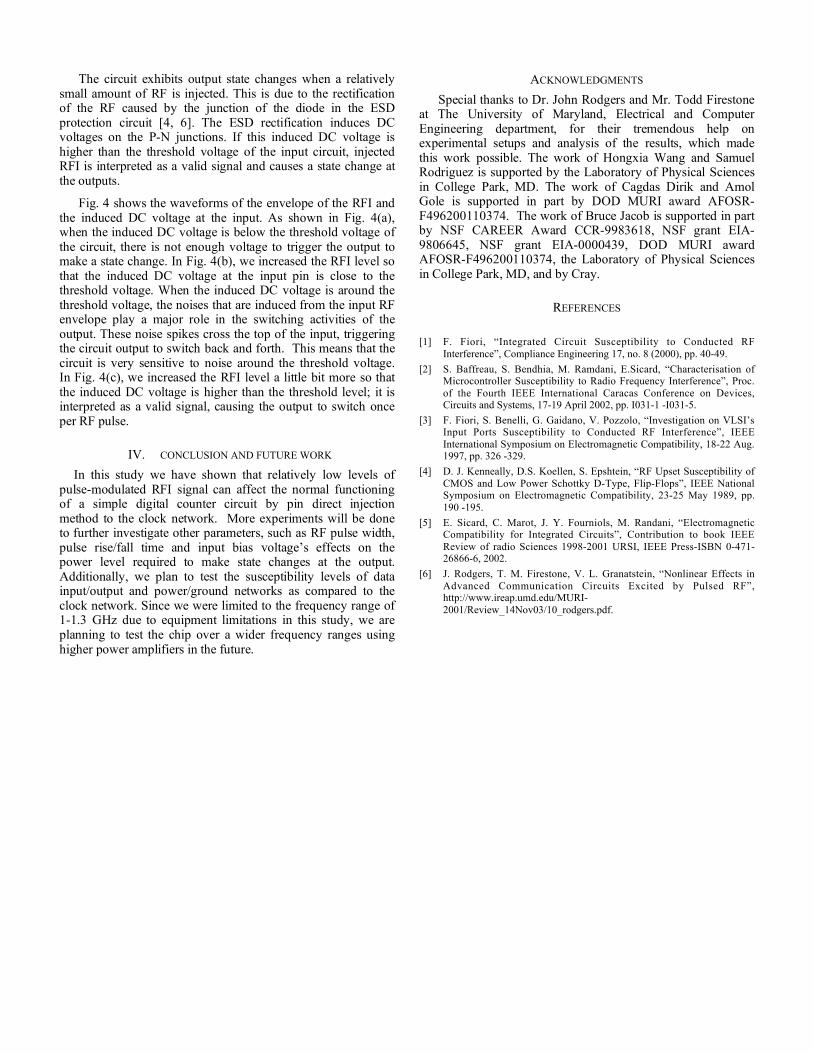
For different frequency and power levels of the injected RFsignal, we observed the least significant bit of the ripplecounter output, CTR [0] in Fig. 2. When RF pulses are coupledinto the input EXTCLK pin of the counter, we noticed clearstate changes at the output, as shown in Fig. 4(c), for a sourcefrequency of 1.0 GHz.
Table 1 summarizes the required RF power levels to makestate changes. PIN stands for power injected; the reflectedpower because of the impedance mismatching is called PR; andthe power that is actually delivered into the pin is named PD.The latter is derived from PIN, and PR. This table also includesthe power-reflection coefficient Γ, which is defined as squareroot of the reflected power PR, versus power injected PIN, andits relationship with power delivered, PIN is shown in Fig. 3.
From Fig. 3 and Table 1, we observe that the inputimpedance of the counter circuit is frequency-dependent; this isbecause of the unmatched load and standing waves. However,this impedance is independent of the injected RF power withthe power level we applied, within which the input device isoperating in the linear region. At the frequency at which thecircuit is more susceptible (i.e., the one at which less power isrequired to make a state change, 1.2 GHz in this case), thepower-reflection coefficient is the lowest. At this frequencythe power coefficient is less than half than those at otherfrequency ranges. This may be caused by the input circuitryresonant frequencies, which are around 1.2 GHz.
Figure 3. Power-reflection coefficient
Table 1. Power required making state changes
(a)
(b)
(c)
(c)
Figure 4. Rectification of RF causing output state changes; (a) Induced inputvoltage is below threshold voltage; no state changes observed at the output; (b)Induced input voltage is right around threshold voltage and RFI induced noisecauses the output to change back and forth; (c) Induced input voltage is abovethreshold voltage; single change at the output is observed
RF Envelope/Input/Output Voltage
-1
1
3
5
0 10 20 30 40
Time (µs)
Vol
tage
(V
) Output VoltageInput VoltageRF Envelope
RF Envelope/Input/Output Voltage
-1
1
3
5
0 10 20 30 40
Time (µs)
Vol
tage
(V
)
RF EnvelopeOutput VoltageInput Voltage
RF Envelope/Input/Output Voltage
-1
1
3
5
0 10 20 30 40
Time (µs)
Vol
tage
(V
)
RF EnvelopeInput VoltageOutput Voltage
Freq (GHz)Power (dBm)
1.0 1.1 1.2 1.3
PIN 20.1 17.9 16.9 20.5
PR 13.3 13.8 6.3 15.3
PD 16.8 15.2 14.7 16.6
Γ 0.559 0.653 0.392 0.652
Power Injected Vs. Reflection Coefficent
0
0.2
0.4
0.6
0 5 10 15 20 25
Power Injected (dBm)
Ref
lect
ion
Coe
ffic
ent
1 GHz1.1 GHz1.2 GHz1.3 GHz
The circuit exhibits output state changes when a relativelysmall amount of RF is injected. This is due to the rectificationof the RF caused by the junction of the diode in the ESDprotection circuit [4, 6]. The ESD rectification induces DCvoltages on the P-N junctions. If this induced DC voltage ishigher than the threshold voltage of the input circuit, injectedRFI is interpreted as a valid signal and causes a state change atthe outputs.
Fig. 4 shows the waveforms of the envelope of the RFI andthe induced DC voltage at the input. As shown in Fig. 4(a),when the induced DC voltage is below the threshold voltage ofthe circuit, there is not enough voltage to trigger the output tomake a state change. In Fig. 4(b), we increased the RFI level sothat the induced DC voltage at the input pin is close to thethreshold voltage. When the induced DC voltage is around thethreshold voltage, the noises that are induced from the input RFenvelope play a major role in the switching activities of theoutput. These noise spikes cross the top of the input, triggeringthe circuit output to switch back and forth. This means that thecircuit is very sensitive to noise around the threshold voltage.In Fig. 4(c), we increased the RFI level a little bit more so thatthe induced DC voltage is higher than the threshold level; it isinterpreted as a valid signal, causing the output to switch onceper RF pulse.
IV. CONCLUSION AND FUTURE WORK
In this study we have shown that relatively low levels ofpulse-modulated RFI signal can affect the normal functioningof a simple digital counter circuit by pin direct injectionmethod to the clock network. More experiments will be doneto further investigate other parameters, such as RF pulse width,pulse rise/fall time and input bias voltage’s effects on thepower level required to make state changes at the output.Additionally, we plan to test the susceptibility levels of datainput/output and power/ground networks as compared to theclock network. Since we were limited to the frequency range of1-1.3 GHz due to equipment limitations in this study, we areplanning to test the chip over a wider frequency ranges usinghigher power amplifiers in the future.
ACKNOWLEDGMENTS
Special thanks to Dr. John Rodgers and Mr. Todd Firestoneat The University of Maryland, Electrical and ComputerEngineering department, for their tremendous help onexperimental setups and analysis of the results, which madethis work possible. The work of Hongxia Wang and SamuelRodriguez is supported by the Laboratory of Physical Sciencesin College Park, MD. The work of Cagdas Dirik and AmolGole is supported in part by DOD MURI award AFOSR-F496200110374. The work of Bruce Jacob is supported in partby NSF CAREER Award CCR-9983618, NSF grant EIA-9806645, NSF grant EIA-0000439, DOD MURI awardAFOSR-F496200110374, the Laboratory of Physical Sciencesin College Park, MD, and by Cray.
REFERENCES
[1] F. Fiori, “Integrated Circuit Susceptibility to Conducted RFInterference”, Compliance Engineering 17, no. 8 (2000), pp. 40-49.
[2] S. Baffreau, S. Bendhia, M. Ramdani, E.Sicard, “Characterisation ofMicrocontroller Susceptibility to Radio Frequency Interference”, Proc.of the Fourth IEEE International Caracas Conference on Devices,Circuits and Systems, 17-19 April 2002, pp. I031-1 -I031-5.
[3] F. Fiori, S. Benelli, G. Gaidano, V. Pozzolo, “Investigation on VLSI’sInput Ports Susceptibility to Conducted RF Interference”, IEEEInternational Symposium on Electromagnetic Compatibility, 18-22 Aug.1997, pp. 326 -329.
[4] D. J. Kenneally, D.S. Koellen, S. Epshtein, “RF Upset Susceptibility ofCMOS and Low Power Schottky D-Type, Flip-Flops”, IEEE NationalSymposium on Electromagnetic Compatibility, 23-25 May 1989, pp.190 -195.
[5] E. Sicard, C. Marot, J. Y. Fourniols, M. Randani, “ElectromagneticCompatibility for Integrated Circuits”, Contribution to book IEEEReview of radio Sciences 1998-2001 URSI, IEEE Press-ISBN 0-471-26866-6, 2002.
[6] J. Rodgers, T. M. Firestone, V. L. Granatstein, “Nonlinear Effects inAdvanced Communication Circuits Excited by Pulsed RF”,http://www.ireap.umd.edu/MURI-2001/Review_14Nov03/10_rodgers.pdf.