Embed Size (px)
Citation preview

Radio Frequency
Integrated Circuits
for 24 GHz
Radar Applications
Peter Lindberg
December 2005
DEPARTMENT OF ENGINEERING SCIENCES
UPPSALA UNIVERSITYUPPSALA, SWEDEN
Submitted to the Faculty of Science and Technology, Uppsala Universityin partial fulfillment of the requirements for the degree of
Licentiate of Technology.

© Peter Lindberg, 2005Printed in Sweden by Eklundshofs Grafiska AB, Uppsala, 2005

To Victoria
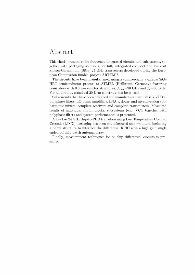
Abstract
This thesis presents radio frequency integrated circuits and subsystems, to-gether with packaging solutions, for fully integrated compact and low costSilicon-Germanium (SiGe) 24 GHz transceivers developed during the Euro-pean Commission funded project ARTEMIS.
The circuits have been manufactured using a commercially available SiGeHBT semiconductor process at ATMEL (Heilbronn, Germany) featuringtransistors with 0.8 µm emitter structures, fmax=90 GHz and fT =80 GHz.For all circuits, standard 20 Ωcm substrate has been used.
Sub-circuits that have been designed and manufactured are 12 GHz VCO:s,polyphase filters, LO pump amplifiers, LNA:s, down- and up-conversion sub-harmonic mixers, complete receivers and complete transmitters. Measuredresults of individual circuit blocks, subsystems (e.g. VCO together withpolyphase filter) and system performances is presented.
A low loss 24 GHz chip-to-PCB transition using Low Temperature Co-firedCeramic (LTCC) packaging has been manufactured and evaluated, includinga balun structure to interface the differential RFIC with a high gain singleended off-chip patch antenna array.
Finally, measurement techniques for on-chip differential circuits is pre-sented.
Acknowledgements
Several people have been essential to the completion of this thesis. Firstand foremost, my thanks goes to my supervisor Prof. Anders Rydberg forhis support and encouragement, and for giving me the chance to work in hisgroup at Uppsala University.
Secondly, I would like to thank my fellow Ph.D. student Erik Ojefors forall his help with circuit design and measurement, and for many interestingdiscussions on work as well as non-work related topics.
Thirdly, my sincere gratitude goes to M.Sc. Zsolt Barna for being my men-tor during my first professional years in the microwave industry, for teachingme all I know about antenna and passive microwave design, and for being agreat friend. Hopefully, we will someday get a chance to work together again.
Fourthly, I would like to thank former ARTEMIS project members Dr. Er-tugrul Sonmez, Dr. Peter Abele and Prof. Hermann Schumacher for theirgreat companionship and for their pioneering work in SiGe RFIC design. Inparticular, Dr Ertugrul Sonmez has given me countless advice on the moreadvanced topics in circuit design as well as providing me with circuits foruse in the receiver and transmitter presented in this thesis.
Fifthly, thanks to my former diploma supervisor and fellow Ph.D studentDr. Dhanesh Kurup for all his invaluable advice and help during my firstexperience in the microwave field (i.e. the diploma work), for continuousdiscussions on various topics and for being a truly nice person.
Finally, I would like to thank all the staff and co-workers at the Signaland Systems Group, for contributing to a nice working atmosphere, and foralways bringing up interesting discussion topics during coffee breaks andlunches.

vi
Contents
1 Introduction 11.1 Background and applications . . . . . . . . . . . . . . . . . . 11.2 Outline of the thesis . . . . . . . . . . . . . . . . . . . . . . . 41.3 Contributions . . . . . . . . . . . . . . . . . . . . . . . . . . . 4
2 System architecture and process technology 72.1 Front End Architecture . . . . . . . . . . . . . . . . . . . . . 72.2 SiGe Semiconductor technology . . . . . . . . . . . . . . . . . 11
2.2.1 Active components . . . . . . . . . . . . . . . . . . . . 142.2.2 Passive components . . . . . . . . . . . . . . . . . . . 17
3 RFIC Subcircuits Design 233.0.3 Interstage Matching (Tuning) . . . . . . . . . . . . . . 233.0.4 DC Biasing Circuitry . . . . . . . . . . . . . . . . . . 243.0.5 Low Noise Amplifier (LNA) . . . . . . . . . . . . . . . 273.0.6 Voltage Controlled Oscillator (VCO) . . . . . . . . . . 303.0.7 Polyphase filter . . . . . . . . . . . . . . . . . . . . . . 353.0.8 LO Pump Amplifiers . . . . . . . . . . . . . . . . . . . 393.0.9 Subharmonic Down-conversion Mixers . . . . . . . . . 403.0.10 Subharmonic Up-conversion Mixers . . . . . . . . . . . 483.0.11 Wilkinson coupler . . . . . . . . . . . . . . . . . . . . 51
4 RFIC Systems 574.0.12 Monolithic Receiver with external LO . . . . . . . . . 574.0.13 Monolithic Receiver with internal LO . . . . . . . . . 60
5 RFIC Packaging using LTCC 63
vii

viii Contents
5.1 LTCC packaging concept . . . . . . . . . . . . . . . . . . . . 635.2 Balun . . . . . . . . . . . . . . . . . . . . . . . . . . . . . . . 655.3 Evaluation PCB . . . . . . . . . . . . . . . . . . . . . . . . . 68
6 Conclusions and future work 716.1 Conclusions . . . . . . . . . . . . . . . . . . . . . . . . . . . . 716.2 Future Work . . . . . . . . . . . . . . . . . . . . . . . . . . . 71
A Measurement Set-up 75A.1 Wafer probing . . . . . . . . . . . . . . . . . . . . . . . . . . . 75
A.1.1 On wafer calibration kit . . . . . . . . . . . . . . . . . 76
Bibliography 79

Chapter 1Introduction
1.1 Background and applications
The license-free 24 GHz industrial, scientific and medical (ISM) band hasbeen identified as a potential host for future Bluetooth-like short-range wire-less systems, but has so far been restrained from widespread consumer de-ployment by the lack of low cost millimeter-wave circuitry with sufficientperformance. While drastically increasing the operating frequency (x10compared to Bluetooth) represents obvious advantages in the form of higherabsolute bandwidths, reduced interference problems (from e.g. microwaveovens, Bluetooth and WLAN), reduced size of antennas and lower healthhazard from EM radiation (due to the smaller penetration depth in humantissue), it also puts higher demands on packaging and semiconductor tech-nology.
This thesis presents the development of RFIC:s and packaging solutionsfor a fully monolithic SiGe based receiver and transmitter front end withinthe European Commission funded project ARTEMIS (’Advanced RF Fron-tend Technology using Micromachined SiGe’), aiming to demonstrate thefeasibility of inexpensive, compact short-range radio frequency subsystemsfor the 24 GHz ISM band. Two main applications for the radio systemswere targeted
• Short range Bluetooth-like communication devices featuring low gainon-chip antennas to remove all chip to chip-carrier high frequency in-terconnects and therefore greatly simplify packaging issues. To in-crease antenna efficiency, the antenna metallization was deposited onthick organic dielectrics (BCB) on top of the silicon wafer, in combi-
1
2 Chapter 1: Introduction
Transmit Antenna Receive Antenna
Teflon substrate
0.5 mm
0.5 mm
LTCCTx RFIC
5 mm
Teflon substrate
Aluminium
Balun Rx RFIC
On-substrate components(eg. power regulator)
Coaxial TL
Microstrip TL
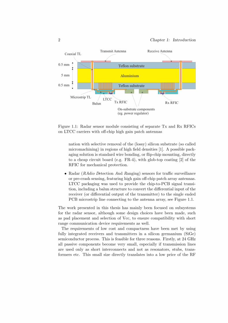
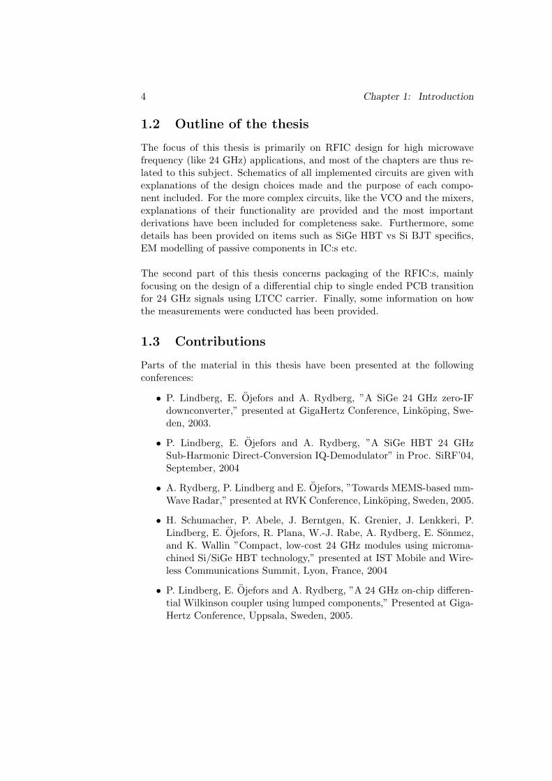
Figure 1.1: Radar sensor module consisting of separate Tx and Rx RFICson LTCC carriers with off-chip high gain patch antennas
nation with selective removal of the (lossy) silicon substrate (so calledmicromachining) in regions of high field densities [1]. A possible pack-aging solution is standard wire bonding, or flip-chip mounting, directlyto a cheap circuit board (e.g. FR-4), with glob-top coating [2] of theRFIC for mechanical protection.
• Radar (RAdio Detection And Ranging) sensors for traffic surveillanceor pre-crash sensing, featuring high gain off-chip patch array antennas.LTCC packaging was used to provide the chip-to-PCB signal transi-tion, including a balun structure to convert the differential input of thereceiver (or differential output of the transmitter) to the single endedPCB microstrip line connecting to the antenna array, see Figure 1.1.
The work presented in this thesis has mainly been focused on subsystemsfor the radar sensor, although some design choices have been made, suchas pad placement and selection of Vcc, to ensure compatibility with shortrange communication device requirements as well.
The requirements of low cost and compactness have been met by usingfully integrated receivers and transmitters in a silicon germanium (SiGe)semiconductor process. This is feasible for three reasons. Firstly, at 24 GHzall passive components become very small, especially if transmission linesare used only as short interconnects and not as resonators, stubs, trans-formers etc. This small size directly translates into a low price of the RF
1.1. Background and applications 3
front-end, especially when compared to the more traditional designs usingdiscrete III-V devices. Secondly, the effective radiated power (EIRP) in the24 GHz ISM (Industrial, Scientific and Medical) band is restricted by Euro-pean Telecommunications Standards Institute (ETSI) regulations [3] to 100mW, meaning that if a 20 dBi gain antenna is used (as in the targeted radarapplication) the power amplifier need only to deliver about 0 dBm (slightlymore to compensate for losses in the balun and interconnects). Thus, sincethe on-chip power levels are low, the thermal effects can be handled evenwith the PA integrated on the same die. Thirdly, both the receiver and thetransmitter have been designed using a direct conversion architecture. Forthe receiver, this means that the high-Q off-chip IF filters and IF down-conversion stages used in a superheterodyne architecture are replaced bylow-pass filters and baseband amplifiers that are easily integrated monolith-ically. Also, no (typically off-chip) image filter is required between the LNAand the mixer.
Earlier work on monolithic transceivers for the 24 GHz band is representedby the phased-array receiver in [4], featuring a 4.8 GHz IF superheterodynearchitecture implemented in a fT = 120 GHz BiCMOS process consuming11.55 mm2 chip area. The targeted applications are ultrahigh-speed wirelesscommunication and long distance radar, making the receiver less suitable forlow-cost short-range applications. No work on a 24 GHz transmitter coun-terpart has been reported so far.
In [5] the first fully monolithic SiGe receiver for the 24 GHz band waspresented. The system features a single-ended superheterodyne receiverimplemented in a fT = 50 GHz HBT process. Later, this work has beenextended into a fully differential design [6] using the same process as inthis thesis. A transmitter has also been developed, reusing most of thecomponents from the receiver. By utilizing an image-rejection architectureno off-chip filters were needed. Fundamental mode mixing (i.e. the VCOoperates at 24 GHz) has been used, implicating a higher susceptibility toDC offsets compared to the subharmonic approach adopted in this thesis.
In [7] a 24 GHz transceiver chip is reported using a fmax = 84 GHzSiGe(C)-HBT:s BiCMOS technology. This work is an extension of a trans-mitter reported in [8]. The transceiver does not include an on-chip LNA,has (only) one single-balanced mixer, is based on a single-ended design us-ing microstrip transmission lines (strip on top layer metal, signal ground onbottom layer metal, silicon dioxide as substrate) both as interconnects andas resonators, and so differs from the work in this thesis in many respects.
4 Chapter 1: Introduction
1.2 Outline of the thesis
The focus of this thesis is primarily on RFIC design for high microwavefrequency (like 24 GHz) applications, and most of the chapters are thus re-lated to this subject. Schematics of all implemented circuits are given withexplanations of the design choices made and the purpose of each compo-nent included. For the more complex circuits, like the VCO and the mixers,explanations of their functionality are provided and the most importantderivations have been included for completeness sake. Furthermore, somedetails has been provided on items such as SiGe HBT vs Si BJT specifics,EM modelling of passive components in IC:s etc.
The second part of this thesis concerns packaging of the RFIC:s, mainlyfocusing on the design of a differential chip to single ended PCB transitionfor 24 GHz signals using LTCC carrier. Finally, some information on howthe measurements were conducted has been provided.
1.3 Contributions
Parts of the material in this thesis have been presented at the followingconferences:
• P. Lindberg, E. Ojefors and A. Rydberg, ”A SiGe 24 GHz zero-IFdownconverter,” presented at GigaHertz Conference, Linkoping, Swe-den, 2003.
• P. Lindberg, E. Ojefors and A. Rydberg, ”A SiGe HBT 24 GHzSub-Harmonic Direct-Conversion IQ-Demodulator” in Proc. SiRF’04,September, 2004
• A. Rydberg, P. Lindberg and E. Ojefors, ”Towards MEMS-based mm-Wave Radar,” presented at RVK Conference, Linkoping, Sweden, 2005.
• H. Schumacher, P. Abele, J. Berntgen, K. Grenier, J. Lenkkeri, P.Lindberg, E. Ojefors, R. Plana, W.-J. Rabe, A. Rydberg, E. Sonmez,and K. Wallin ”Compact, low-cost 24 GHz modules using microma-chined Si/SiGe HBT technology,” presented at IST Mobile and Wire-less Communications Summit, Lyon, France, 2004
• P. Lindberg, E. Ojefors and A. Rydberg, ”A 24 GHz on-chip differen-tial Wilkinson coupler using lumped components,” Presented at Giga-Hertz Conference, Uppsala, Sweden, 2005.

1.3. Contributions 5
• P. Lindberg, E. Ojefors and A. Rydberg, ”A SiGe 24 GHz monolith-ically integrated direct conversion receiver,” Presented at GigaHertzConference, Uppsala, Sweden, 2005.
• P. Lindberg, E. Ojefors and A. Rydberg, ”LTCC packaging for a 26GHz SiGe receiver,” Presented at GigaHertz Conference, Uppsala,Sweden, 2005.

6 Chapter 1: Introduction
Chapter 2System architecture and process
technology
2.1 Front End Architecture
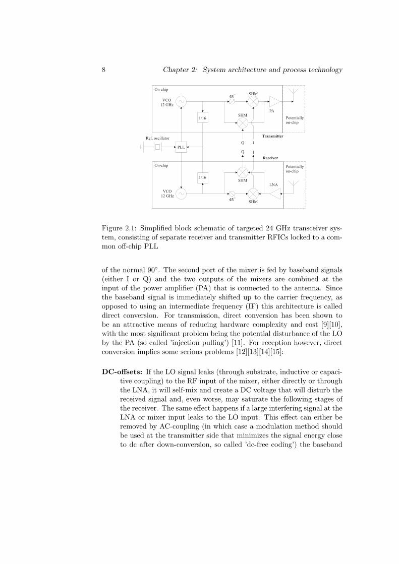
The 24 GHz transceiver developed within the ARTEMIS project was di-vided into separate transmitter and receiver chips, see Figure 2.1, due toisolation constraints and to relax heat dissipating requirements of the chipcarriers. For cost and packaging reasons, the circuits have been implementedmonolithically, which was made possible by the choice of a direct conversionarchitecture. The receiver front-end is schematically shown in Figure 2.2.The transmitter shares almost all subcomponents with the receiver, withthe exception of the LNA being replaced by a PA and a modified mixercore used for up-conversion. All circuits are designed for a unipolar supplyvoltage of 3V.
The main building blocks of the front end are shown in Figure 2.1. Lookingat the transmitter (at the top) section of the transceiver, a VCO (VoltageControlled Oscillator) produces a 12 GHz signal that is fed to two mixers 45
out of phase. In the more traditional case (called ”fundamental mixing”), a24 GHz LO signal would have been fed to the two mixers 90 out of phase forI/Q-modulation. In the architecture employed in this work, the mixers havebeen designed to operate at twice the LO frequency (so called ”sub-harmonicmixing”), meaning that there is an intrinsic frequency (x2) multiplicationinside the mixer that will also double the phase shift, hence the 45 instead
7
8 Chapter 2: System architecture and process technology
PLL
1/16
PA
Ref. oscillatorIQ
Transmitter
VCO12 GHz
45
SHM
SHM
1/16
LNA
IQ
Receiver
VCO12 GHz
45
SHM
SHM
On-chip
On-chip
Potentiallyon-chip
Potentiallyon-chip
Figure 2.1: Simplified block schematic of targeted 24 GHz transceiver sys-tem, consisting of separate receiver and transmitter RFICs locked to a com-mon off-chip PLL
of the normal 90. The second port of the mixer is fed by baseband signals(either I or Q) and the two outputs of the mixers are combined at theinput of the power amplifier (PA) that is connected to the antenna. Sincethe baseband signal is immediately shifted up to the carrier frequency, asopposed to using an intermediate frequency (IF) this architecture is calleddirect conversion. For transmission, direct conversion has been shown tobe an attractive means of reducing hardware complexity and cost [9][10],with the most significant problem being the potential disturbance of the LOby the PA (so called ’injection pulling’) [11]. For reception however, directconversion implies some serious problems [12][13][14][15]:
DC-offsets: If the LO signal leaks (through substrate, inductive or capaci-tive coupling) to the RF input of the mixer, either directly or throughthe LNA, it will self-mix and create a DC voltage that will disturb thereceived signal and, even worse, may saturate the following stages ofthe receiver. The same effect happens if a large interfering signal at theLNA or mixer input leaks to the LO input. This effect can either beremoved by AC-coupling (in which case a modulation method shouldbe used at the transmitter side that minimizes the signal energy closeto dc after down-conversion, so called ’dc-free coding’) the baseband

2.1. Front End Architecture 9
signal, or, as in this work, by using sub-harmonic mixing (i.e. the LOand RF frequencies are separated).
I/Q mismatch: Since the 24 GHz signal is directly converted to basebandI and Q signals, it is more difficult to provide a perfect 90 phase sepa-ration and equal magnitudes compared to when down-converting froman IF frequency (as in superheterodyne receivers). This means thatthe received signal constellation will be altered, increasing the bit errorrate. This problem is more pronounced in discrete designs and tends tobe less severe with high levels of integration. No special method (suchas using I/Q calibration look-up tables), except for highly symmetriclayouts, have been attempted to reduce the I/Q mismatch.
Even-order distortion: If two strong, closely spaced (in frequency) in-terfering signals are present at the input of the LNA, any even ordernon-linearity in the amplifier will produce low-frequency beats at thedifference frequency of the two signals. This term is fed to the RF-input of the mixer, where it would ideally be translated to a highfrequency and removed by the output filter. However, as there is afinite direct feed-through from the RF to the baseband ports in allreal mixers, some of it will appear at the output corrupting the re-ceived signal. By using a completely differential system, all even-orderdistortion is (ideally) removed.
1/f noise: As the received signal is directly converted to DC and is onlyamplified by the LNA and mixer prior to this, any 1/f (flicker) noisepresent at the output will greatly reduce the signal to noise ratio. Thisproblem is more severe in CMOS technologies, with typical cornerfrequencies of a few MHz, than in bipolar technologies with typicalcorner frequencies of a few kHz. No special techniques, other than theusage of bipolar transistors, have been used to counter this effect.
To provide a clean LO signal without temperature and time drift and withlow phase noise, the VCO should be phase-locked to an off-chip crystal oscil-lator (a so called phase locked loop, PLL). Since there are no commerciallyavailable PLL:s working at 12 GHz, the VCO is connected to a frequencydivider (or prescaler) that divides the frequency by a factor of 16, providingfor a simpler off-chip transition and cheaper PLL circuit.
By connecting the VCO:s of the receiver and the transmitter to the samePLL, the LO signals in the receiver and transmitter can be phase synchro-nized, which is required by the radar application. Furthermore, by using IQ

10 Chapter 2: System architecture and process technology
modulation and demodulation, the phase and amplitude of the carrier (24GHz) signal is easily controlled, implying that any modulation method (likeBPSK, QPSK, 16 QAM etc) can be used.
A more complete schematic, with buffer and pump amplifiers included, ofthe receiver (with the transmitter being identical except for the LNA beingreplaced by a PA) is shown in Figure 2.2. As all components are eitherdesigned to be narrow banded (e.g. to get as much gain as possible fromthe active devices in amplifiers) or are narrow-banded by nature (e.g. thepolyphase filter), there is a distributed filter action taken place throughoutthe system in addition to the explicit low-pass filters following the mixers.
00
00
1800
900
1800
2700
450
1350
2250
3150
Polyphase filter
II
IQ
QI
LO amplifiers
RF in (out)
Mixers
Baseband I
Baseband Q
2 p
ole
s1 p
ole
LNA (PA)
VCO
12 GHzBufferamplifierPLL
1/16
Crystal refoscillator
On chipPotentiallyon-chip
Off chip
LPF
LPF
Figure 2.2: Block schematic of receiver and transmitter
By using sub-harmonic x2 mixing in the IQ-(de)modulator and a fullydifferential topology, several advantages are obtained:
• The VCO operates at half the RF frequency (i.e. 12 GHz) resulting in
1. a larger unstable region of the active devices, making the oscil-lator less sensitive to terminating and load impedances. In con-trast, oscillators working close to fmax may require many designiterations just to achieve oscillation start-up.
2. higher resonator Q (on-chip LC tank), translating into lowerphase noise and higher output power. The higher gain of theactive devices at 12 GHz further increases the maximum avail-able output power. These advantages are however counter-actedat the system level by the intrinsic frequency doubler in the mixer

2.2. SiGe Semiconductor technology 11
adding 6 dB to the phase noise, and the LO input ports of themixers consuming more (x2) power than an ordinary mixer
3. no disturbance of the transmit LO by the PA (s.c. ”injectionpulling” or ”injection locking”) since the output frequency is notclose to the oscillating frequency
4. no LO power at 24 GHz (from second order non-linearities) be-cause of the differential output
5. reduced LO to antenna coupling (from the inductor in the res-onator tank) when using an on-chip antenna, since as the couplinghas a maximum at the antenna resonance frequency, which is farfrom the LO frequency
• no DC offsets from LO self-mixing since there is (ideally) no LO signalat the RF frequency
• no base-band offsets from second order distortion of RF input signalsbecause of the differential topology
• reduced cross-talk between circuit blocks from supply and ground sig-nal disturbances because of (ideally) no high-frequency currents inVcc lines or ground. This can be even more important in mixed sig-nal environments, for example with PLL circuitry on-chip, where e.g.transients from digitial switching can severly degrade system perfor-mance
• higher output power is available from the active devices due to thedifferential design. The output power, which in terms of voltage islimited by the breakdown voltage of the transistors (somewhere be-tween BVCEO and BVCBO - usually closer to BVCBO in a real circuit[16]) is increased due to the effective ”doubling” of the breakdownvoltages of the transistors, i.e. only half the output voltage is overeach transistor.
2.2 SiGe Semiconductor technology
The circuits have been realized in Atmels Silicon Germanium (SiGe) hetero-junction bipolar transistor (HBT) semiconductor process SiGe2RF [17], fea-turing a 0.8 µm lithography, 3 metal layers (see Figure 2.3), MIM-capacitors,4 resistor types, lateral PNP:s and pn/zener/varactor/schottky-diodes. Im-portant advantages of SiGe HBTs over III-V devices (such as GaAs or InP)
12 Chapter 2: System architecture and process technology
more commonly used at high microwave frequencies, are that, as they aresilicon based, they
• have lower price
• have higher yield
• are compatible with CMOS technology (s.c. BiCMOS)
• have better thermal properties
• are process compatible with etching techniques
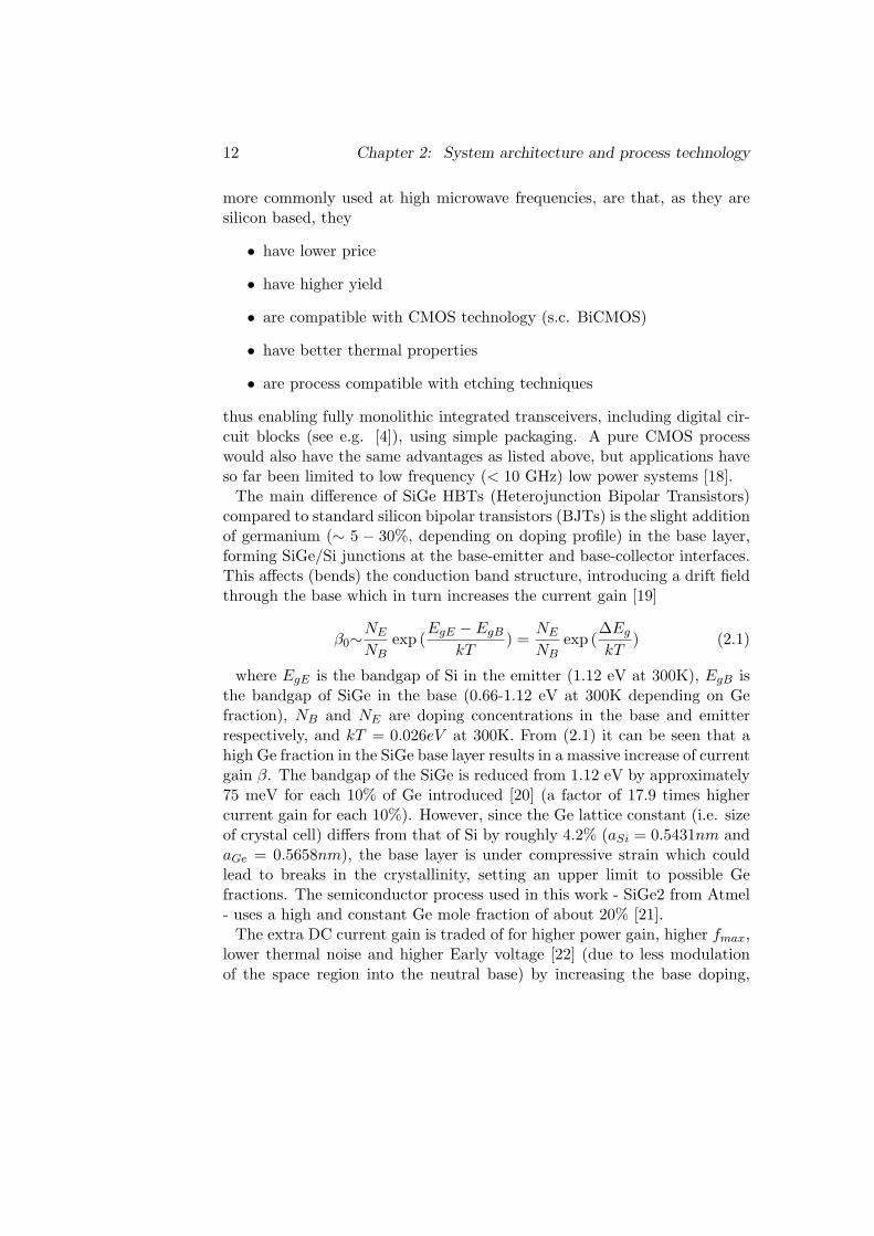
thus enabling fully monolithic integrated transceivers, including digital cir-cuit blocks (see e.g. [4]), using simple packaging. A pure CMOS processwould also have the same advantages as listed above, but applications haveso far been limited to low frequency (< 10 GHz) low power systems [18].
The main difference of SiGe HBTs (Heterojunction Bipolar Transistors)compared to standard silicon bipolar transistors (BJTs) is the slight additionof germanium (∼ 5 − 30%, depending on doping profile) in the base layer,forming SiGe/Si junctions at the base-emitter and base-collector interfaces.This affects (bends) the conduction band structure, introducing a drift fieldthrough the base which in turn increases the current gain [19]
β0∼NE
NBexp (
EgE − EgB
kT) =
NE
NBexp (
∆Eg
kT) (2.1)
where EgE is the bandgap of Si in the emitter (1.12 eV at 300K), EgB isthe bandgap of SiGe in the base (0.66-1.12 eV at 300K depending on Gefraction), NB and NE are doping concentrations in the base and emitterrespectively, and kT = 0.026eV at 300K. From (2.1) it can be seen that ahigh Ge fraction in the SiGe base layer results in a massive increase of currentgain β. The bandgap of the SiGe is reduced from 1.12 eV by approximately75 meV for each 10% of Ge introduced [20] (a factor of 17.9 times highercurrent gain for each 10%). However, since the Ge lattice constant (i.e. sizeof crystal cell) differs from that of Si by roughly 4.2% (aSi = 0.5431nm andaGe = 0.5658nm), the base layer is under compressive strain which couldlead to breaks in the crystallinity, setting an upper limit to possible Gefractions. The semiconductor process used in this work - SiGe2 from Atmel- uses a high and constant Ge mole fraction of about 20% [21].
The extra DC current gain is traded of for higher power gain, higher fmax,lower thermal noise and higher Early voltage [22] (due to less modulationof the space region into the neutral base) by increasing the base doping,
2.2. SiGe Semiconductor technology 13
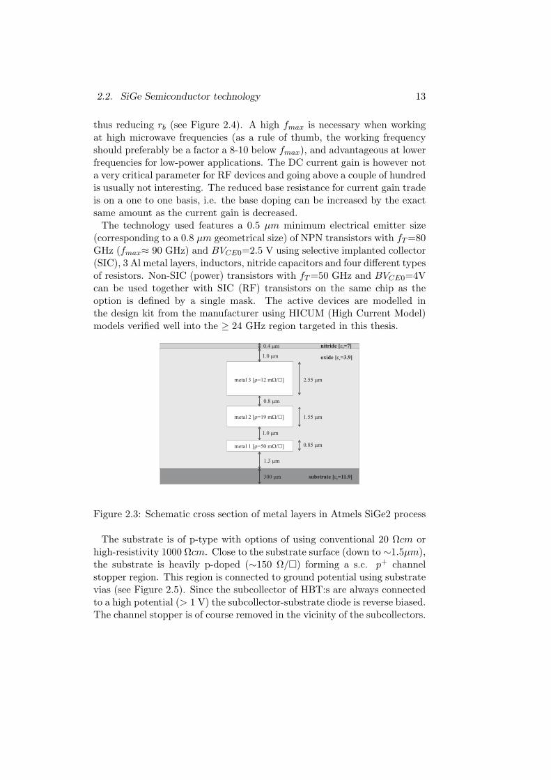
thus reducing rb (see Figure 2.4). A high fmax is necessary when workingat high microwave frequencies (as a rule of thumb, the working frequencyshould preferably be a factor a 8-10 below fmax), and advantageous at lowerfrequencies for low-power applications. The DC current gain is however nota very critical parameter for RF devices and going above a couple of hundredis usually not interesting. The reduced base resistance for current gain tradeis on a one to one basis, i.e. the base doping can be increased by the exactsame amount as the current gain is decreased.
The technology used features a 0.5 µm minimum electrical emitter size(corresponding to a 0.8 µm geometrical size) of NPN transistors with fT =80GHz (fmax≈ 90 GHz) and BVCE0=2.5 V using selective implanted collector(SIC), 3 Al metal layers, inductors, nitride capacitors and four different typesof resistors. Non-SIC (power) transistors with fT =50 GHz and BVCE0=4Vcan be used together with SIC (RF) transistors on the same chip as theoption is defined by a single mask. The active devices are modelled inthe design kit from the manufacturer using HICUM (High Current Model)models verified well into the ≥ 24 GHz region targeted in this thesis.
substrate [ =11.9]er
1.3 mm
oxide [ =3.9]er
nitride [ =7]er
300 mm
0.85 mm
1.0 mm
1.55 mm
0.8 mm
2.55 mm
1.0 mm
0.4 mm
metal 1 [ =50 m ]r W/Ö
metal 2 [ =19 m ]r W/Ö
metal 3 [ =12 m ]r W/Ö
Figure 2.3: Schematic cross section of metal layers in Atmels SiGe2 process
The substrate is of p-type with options of using conventional 20 Ωcm orhigh-resistivity 1000 Ωcm. Close to the substrate surface (down to ∼1.5µm),the substrate is heavily p-doped (∼150 Ω/) forming a s.c. p+ channelstopper region. This region is connected to ground potential using substratevias (see Figure 2.5). Since the subcollector of HBT:s are always connectedto a high potential (> 1 V) the subcollector-substrate diode is reverse biased.The channel stopper is of course removed in the vicinity of the subcollectors.
14 Chapter 2: System architecture and process technology
Traditionally, there has been a substantial price difference between highand low ohmic substrates, but today that is no longer true. The mainadvantages of the 1000 Ωcm substrate are lower collector-substrate capaci-tance (due to the depletion layer extending further into the substrate) andhigher Q-values of passive structures such as inductors, transmission linesand antennas. The main disadvantage is the increase of transistor spacingnecessary to avoid the depletion layers of the sub-collectors to meet, makinglayouts more sparse which in turn leads to increased losses and impedancemismatches from interconnect lines. Also, high resistivity substrate is notcompatible with CMOS circuitry. To summarize, the substrates have differ-ent merits and the selection will be dependent on the application.
2.2.1 Active components
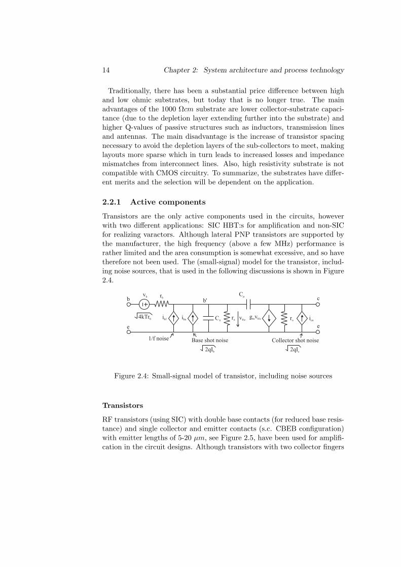
Transistors are the only active components used in the circuits, howeverwith two different applications: SIC HBT:s for amplification and non-SICfor realizing varactors. Although lateral PNP transistors are supported bythe manufacturer, the high frequency (above a few MHz) performance israther limited and the area consumption is somewhat excessive, and so havetherefore not been used. The (small-signal) model for the transistor, includ-ing noise sources, that is used in the following discussions is shown in Figure2.4.
rpCp
b
e e
cb'rb
roibf ibn
Cm
Collector shot noise
vb
Base shot noise1/f noise
icngmvb'evb'e
4kTrb
2qIb 2qIc
Figure 2.4: Small-signal model of transistor, including noise sources
Transistors
RF transistors (using SIC) with double base contacts (for reduced base resis-tance) and single collector and emitter contacts (s.c. CBEB configuration)with emitter lengths of 5-20 µm, see Figure 2.5, have been used for amplifi-cation in the circuit designs. Although transistors with two collector fingers
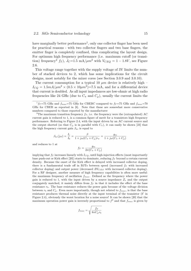
2.2. SiGe Semiconductor technology 15
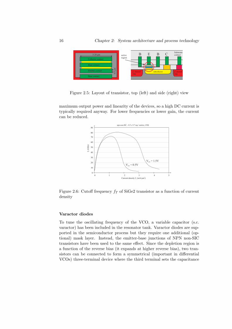
have marginally better performance1, only one collector finger has been usedfor practical reasons - with two collector fingers and two base fingers, theemitter finger is completely confined, thus complicating the layout design.For optimum high frequency performance (i.e. maximum cutoff (or transi-tion) frequency2 fT ), JC=1.5 mA/µm2 with VCEQ = 1 − 1.8V , see Figure2.6.
This voltage range together with the supply voltage of 3V limits the num-ber of stacked devices to 2, which has some implications for the circuitdesigns, most notably for the mixer cores (see Section 3.0.9 and 3.0.10).
The current consumption for a typical 10 µm device is relatively high –ICQ = 1.5mA/µm2 × (0.5 × 10µm2)=7.5 mA, and for a differential devicethat current is doubled. As all input impedances are low-ohmic at high radiofrequencies like 24 GHz (due to Cπ and Cµ), usually the current limits the
1fT =75 GHz and fmax=75 GHz for CBEBC compared to fT =75 GHz and fmax=70GHz for CBEB as reported in [6]. Note that these are somewhat more conservativenumbers compared to those reported by the manufacturer
2The maximum transition frequency fT , i.e. the frequency were the (extrapolated) ACcurrent gain is reduced to 1, is a common figure of merit for a transistors high frequencyperformance. Referring to Figure 2.4, with the input driven by an AC current source andthe output shorted (so that Cµ is in parallel with Cπ), it can easily be shown [23] thatthe high frequency current gain βac is equal to
βac(jω) =Ic
Ib
=β
1 + jω(Cπ + Cµ)rπ
=gm
1 + jω(Cπ + Cµ)
and reduces to 1 at
fT =gm
2π(Cπ + Cµ)
implying that fT increases linearly with ICQ, until high-injection effects (most importantlybase push-out or Kirk effect [20]) starts to dominate, reducing fT beyond a certain currentdensity. Because the onset of the Kirk effect is delayed with increased collector doping,there is a fundamental trade off in BJTs between speed (increased fT with increasedcollector doping) and output power (decreased BVCEO with increased collector doping).For a RF designer, another measure of high frequency capabilities is often more useful:the maximum frequency of oscillation fmax. Defined as the frequency where the powergain is reduced to 1, with the input driven by a source impedance Zs and the outputconjugately matched, it mainly differs from fT in that it includes the effect of the baseresistance rb. The base resistance reduces the power gain because of the voltage divisionbetween rb and Cµ. Even more importantly, though not related to fmax, is that the baseresistance produces thermal noise directly at the input terminal of the transistor (b′ inFigure 2.4), obviously the worst location for a noise source! It can be shown [20] that themaximum operation power gain is inversely proportional to f2 and that fmax is given by
fmax =
s
fT
8πCµrb
16 Chapter 2: System architecture and process technology
Base contact
Collector contact
Emitter contact
Base contact
p -channelstop
+
CBEB
subcollector p -channelstop
+
activeregion
Substratecontact5-20 mm
0.8
mm
Figure 2.5: Layout of transistor, top (left) and side (right) view
maximum output power and linearity of the devices, so a high DC current istypically required anyway. For lower frequencies or lower gain, the currentcan be reduced.
V = 0.5VCE
V = 1.5VCE
1
Current density J (mA/ m )c m2
f(G
Hz)
T
2 3 4 5
10
20
30
40
50
60
70
80
90
0
0
npn non-SIC - 0.5 x 9.7 m emitter, CEBm2
Figure 2.6: Cutoff frequency fT of SiGe2 transistor as a function of currentdensity
Varactor diodes
To tune the oscillating frequency of the VCO, a variable capacitor (s.c.varactor) has been included in the resonator tank. Varactor diodes are sup-ported in the semiconductor process but they require one additional (op-tional) mask layer. Instead, the emitter-base junctions of NPN non-SICtransistors have been used to the same effect. Since the depletion region isa function of the reverse bias (it expands at higher reverse bias), two tran-sistors can be connected to form a symmetrical (important in differentialVCOs) three-terminal device where the third terminal sets the capacitance
2.2. SiGe Semiconductor technology 17
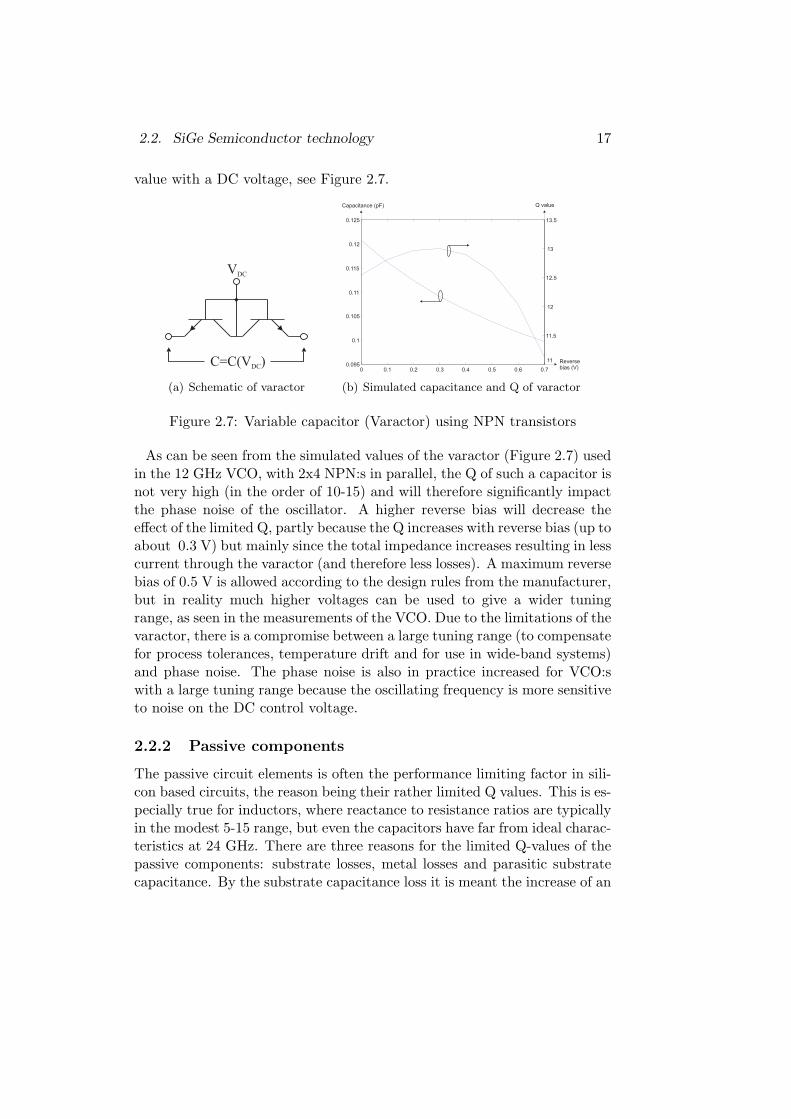
value with a DC voltage, see Figure 2.7.
VDC
C=C(V )DC
(a) Schematic of varactor
0 0.1 0.2 0.3 0.4 0.5 0.6 0.70.095
0.1
0.105
0.11
0.115
0.12
0.125
11
11.5
12
12.5
13
13.5
Reversebias (V)
Capacitance (pF) Q value
(b) Simulated capacitance and Q of varactor
Figure 2.7: Variable capacitor (Varactor) using NPN transistors
As can be seen from the simulated values of the varactor (Figure 2.7) usedin the 12 GHz VCO, with 2x4 NPN:s in parallel, the Q of such a capacitor isnot very high (in the order of 10-15) and will therefore significantly impactthe phase noise of the oscillator. A higher reverse bias will decrease theeffect of the limited Q, partly because the Q increases with reverse bias (up toabout 0.3 V) but mainly since the total impedance increases resulting in lesscurrent through the varactor (and therefore less losses). A maximum reversebias of 0.5 V is allowed according to the design rules from the manufacturer,but in reality much higher voltages can be used to give a wider tuningrange, as seen in the measurements of the VCO. Due to the limitations of thevaractor, there is a compromise between a large tuning range (to compensatefor process tolerances, temperature drift and for use in wide-band systems)and phase noise. The phase noise is also in practice increased for VCO:swith a large tuning range because the oscillating frequency is more sensitiveto noise on the DC control voltage.
2.2.2 Passive components
The passive circuit elements is often the performance limiting factor in sili-con based circuits, the reason being their rather limited Q values. This is es-pecially true for inductors, where reactance to resistance ratios are typicallyin the modest 5-15 range, but even the capacitors have far from ideal charac-teristics at 24 GHz. There are three reasons for the limited Q-values of thepassive components: substrate losses, metal losses and parasitic substratecapacitance. By the substrate capacitance loss it is meant the increase of an
18 Chapter 2: System architecture and process technology
already existing resistive part caused by the parallel capacitance to ground,i.e. not associated with any losses from this coupling.
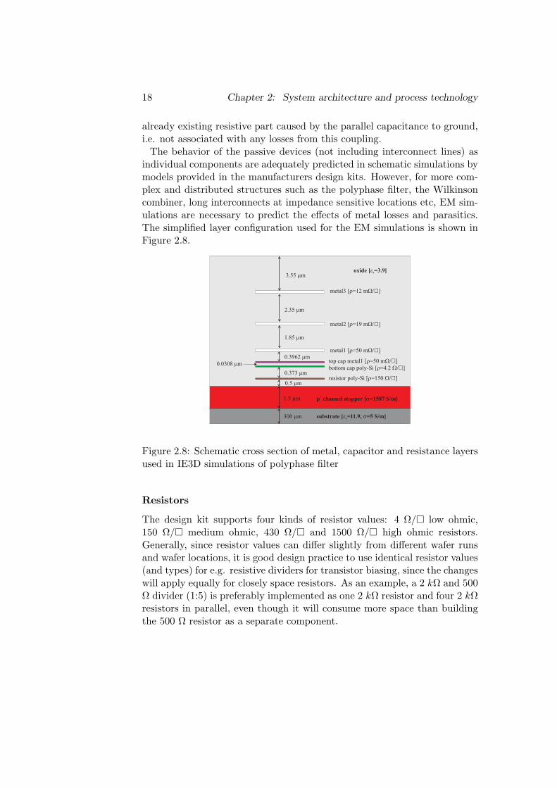
The behavior of the passive devices (not including interconnect lines) asindividual components are adequately predicted in schematic simulations bymodels provided in the manufacturers design kits. However, for more com-plex and distributed structures such as the polyphase filter, the Wilkinsoncombiner, long interconnects at impedance sensitive locations etc, EM sim-ulations are necessary to predict the effects of metal losses and parasitics.The simplified layer configuration used for the EM simulations is shown inFigure 2.8.
substrate [ =11.9, =5 S/m]e sr
0.5 mm
oxide [ =3.9]er
300 mm
1.85 mm
2.35 mm
3.55 mm
metal1 [ =50 m ]r W/Ö
metal2 [ =19 m ]r W/Ö
metal3 [ =12 m ]r W/Ö
p channel stopper [ =1587 S m]+
s /1.5 mm
resistor poly-Si [ =150 ]r W/Ö
bottom cap poly-Si [ =4.2 ]r W/Ö
top cap metal1 [ =50 m ]r W/Ö
0.373 mm
0.0308 mm
0.3962 mm
Figure 2.8: Schematic cross section of metal, capacitor and resistance layersused in IE3D simulations of polyphase filter
Resistors
The design kit supports four kinds of resistor values: 4 Ω/ low ohmic,150 Ω/ medium ohmic, 430 Ω/ and 1500 Ω/ high ohmic resistors.Generally, since resistor values can differ slightly from different wafer runsand wafer locations, it is good design practice to use identical resistor values(and types) for e.g. resistive dividers for transistor biasing, since the changeswill apply equally for closely space resistors. As an example, a 2 kΩ and 500Ω divider (1:5) is preferably implemented as one 2 kΩ resistor and four 2 kΩresistors in parallel, even though it will consume more space than buildingthe 500 Ω resistor as a separate component.
2.2. SiGe Semiconductor technology 19
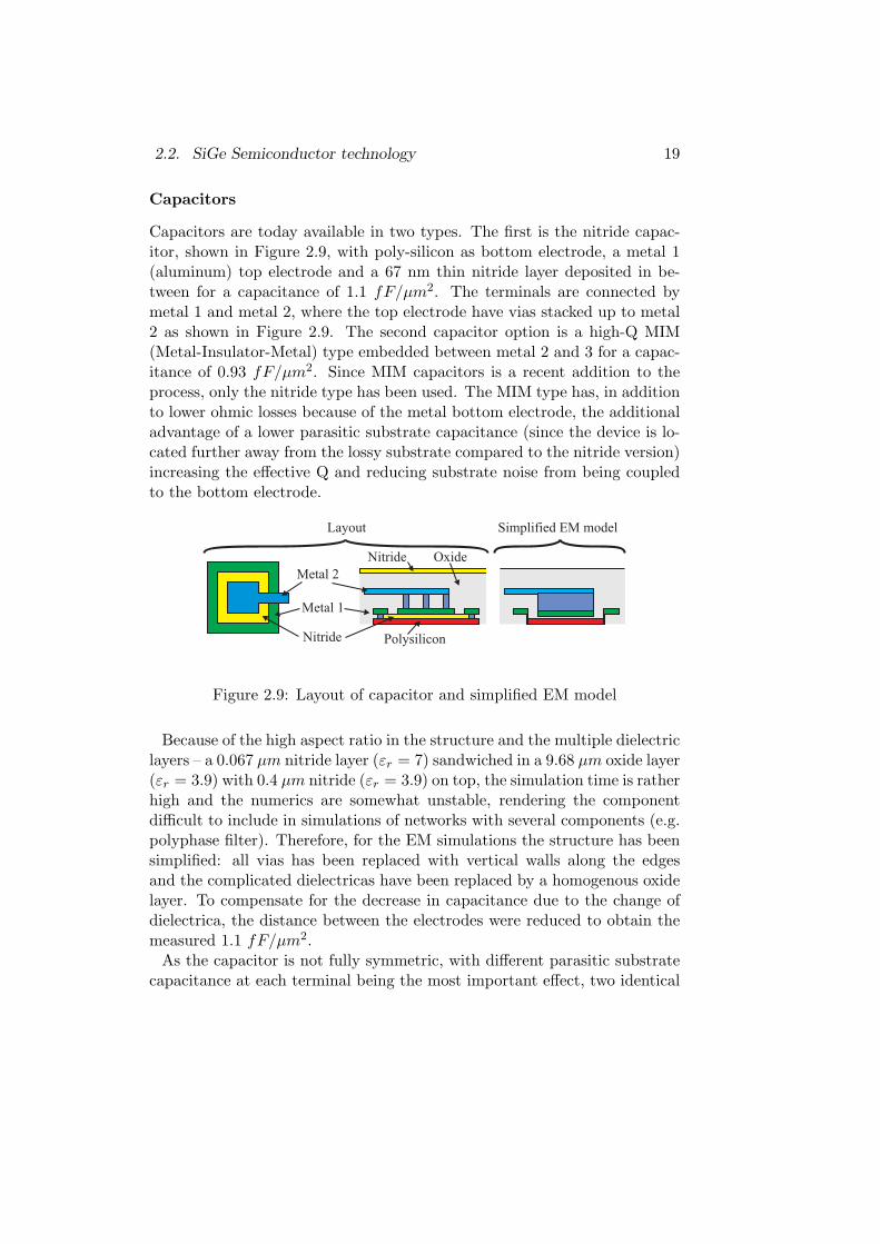
Capacitors
Capacitors are today available in two types. The first is the nitride capac-itor, shown in Figure 2.9, with poly-silicon as bottom electrode, a metal 1(aluminum) top electrode and a 67 nm thin nitride layer deposited in be-tween for a capacitance of 1.1 fF/µm2. The terminals are connected bymetal 1 and metal 2, where the top electrode have vias stacked up to metal2 as shown in Figure 2.9. The second capacitor option is a high-Q MIM(Metal-Insulator-Metal) type embedded between metal 2 and 3 for a capac-itance of 0.93 fF/µm2. Since MIM capacitors is a recent addition to theprocess, only the nitride type has been used. The MIM type has, in additionto lower ohmic losses because of the metal bottom electrode, the additionaladvantage of a lower parasitic substrate capacitance (since the device is lo-cated further away from the lossy substrate compared to the nitride version)increasing the effective Q and reducing substrate noise from being coupledto the bottom electrode.
Metal 1
Metal 2
Nitride Polysilicon
Simplified EM model
Nitride
Layout
Oxide
Figure 2.9: Layout of capacitor and simplified EM model
Because of the high aspect ratio in the structure and the multiple dielectriclayers – a 0.067 µm nitride layer (εr = 7) sandwiched in a 9.68 µm oxide layer(εr = 3.9) with 0.4 µm nitride (εr = 3.9) on top, the simulation time is ratherhigh and the numerics are somewhat unstable, rendering the componentdifficult to include in simulations of networks with several components (e.g.polyphase filter). Therefore, for the EM simulations the structure has beensimplified: all vias has been replaced with vertical walls along the edgesand the complicated dielectricas have been replaced by a homogenous oxidelayer. To compensate for the decrease in capacitance due to the change ofdielectrica, the distance between the electrodes were reduced to obtain themeasured 1.1 fF/µm2.
As the capacitor is not fully symmetric, with different parasitic substratecapacitance at each terminal being the most important effect, two identical
20 Chapter 2: System architecture and process technology
capacitors can be placed in a series back-to-back configuration to ensure fullsymmetry. This however reduces the total capacitance of the device to halfthe value of each capacitor
Inductors
Since all on-wafer impedances at 24 GHz are by nature capacitive, induc-tors are extensively used for impedance matching. Also, since the outputimpedances of the active devices are not very high in this frequency region,and since they consume 1 V for proper functionality, inductors are in someinstances used as (high frequency) current sources for common mode re-jection. Finally, inductors are used for noise-less emitter degeneration toincrease linearity and input impedances of the amplifiers. Although spiralinductors are supported by the design kit, all inductors have been tailormade in IE3D to optimize the structures for the different applications andto include the effects of the surrounding layout and interconnect lines.
High-Q inductors, for instance when used as collector loading in amplifiersor the resonator tank in the VCO, have spiral inductors using metal 2 andmetal 3 in parallel with multiple vias connecting the layers. For applicationswhere the Q is not as critical, like in current sources, the inductors have beenrealized as circular spirals starting at metal 3 and spiraling down to metal1. This way the area consumption is kept to a minimum.
Directly below the inductors, the p+-channel stopper has been removed toincrease the Q-value by avoiding eddy currents and reducing the capacitivecoupling. Further techniques to reduce losses, although not used in thiswork, include a patterned ground shield to reduce the capacitive coupling tothe substrate while blocking magnetically generated currents (which wouldreduce the inductance) [24]. A guard ring of metal 1 and 2, connected tothe substrate by vias, surrounds all inductors to reduce coupling betweenthe inductors [25] and to provide a co-planar ground plane.
Transmission lines (interconnects)
Transmission line structures for conventional silicon processes have receivedconsiderable attention during the last decade, mainly focusing on coplanarwaveguide [26] and microstrip lines [27]. Because of the differential topology,the only transmission line structure of interest in this work is the coplanarstripline (CPS) consisting of two side-by-side metal strips, see Figure 2.11.Due to the high losses in the 20 Ωcm silicon substrate and the excessive areaconsumption, transmission lines have only been used as circuit interconnects

2.2. SiGe Semiconductor technology 21
Ind
Vcc
p+ removal boundary Metal 1 & 2 guard ring
Via metal 1-2
Substrate contact
Via metal 2-3
Figure 2.10: Layout of high (left) and low (right) Q inductors
and not as matching stubs or resonators.Design techniques to reduce losses includes:
• Removing the p+-channel stopper under the coplanar strips [28] (as isdone with inductors and on-chip antennas)
• Using wide strips in the top-most metal layer (metal 3) (which is alsothe thickest metal layer) to reduce metal losses and parasitic substratecoupling
• Reducing the slot width between the CPS lines to confine the fieldlines away from the substrate. This is limited by design rules to 1 µmin metal1, 2 µm in metal2, and 3 µm in metal3
CPS lines with high Z0 can be used to partly compensate for the (par-asitic) capacitive nature of all input impedances in the high-GHz region.However, this approach would be very hard to implement in a practicaldesign due to modelling problems and design complexity. Instead, the pre-ferred choice in this work has been to minimize the length of all interconnectlines and use CPS structures with as low Z0 as possible within the limits ofthe technology (i.e. metal spacing). This means using as small a distancebetween the lines as possible and keeping the ground layer close. The lowZ0 is necessary since all impedances are by nature low ohmic at these el-evated frequencies, so a low characteristic impedance introduces minimumimpedance transformations.
The minimum trace width is limited by current handling capabilities ofthe metal, with electron migration being the main mechanism for loss of

22 Chapter 2: System architecture and process technology
Metal1+Metal2
Substrate via
Metal1-2 via
p channel stopper+
Metal2
Oxide
Top view Side view
Figure 2.11: Layout of CPS transmission line
reliability. In the used process, metal 1-3 has 3, 5 och 8 mA/µm maximumDC current/width respectively. The AC component of the currents cantypically be much larger, with a factor 4 often used [16].

Chapter 3RFIC Subcircuits Design
3.0.3 Interstage Matching (Tuning)
Conjugate matching between inputs and outputs of circuit blocks is wellknown to provide maximum power transfer from source to load. In mostinstances, such as at the amplifier-filter or antenna-transmission line inter-faces, it is obvious why maximum power transfer is desired. However, insome cases the conjugate match also provides optimum circuit performanceeven though power transfer per se is not the objective. Such cases are forexample the LO and RF inputs of the mixer cores. By conjugate match-ing these inputs, maximum voltage swing is obtained at the bases of theswitching transistors and maximum RF currents are supplied at the emit-ters of same transistors, hence resulting in maximum conversion gain andminimum noise of the circuit (see Section 3.0.9). As a side-effect, thereis also maximum current input at the bases and maximum voltage swingat the emitters, but these have no positive influence on the circuit perfor-mance (in fact quite the opposite, since the voltage swing at the emitterscauses non-linearities and the LO pump amplifiers must be sized to supplylarge currents into the bases). For these reasons, the conjugate match isthe most common type of impedance matching. For ease of measurementand to make the circuits more general, it is customary to provide conjugatematches at all circuit interfaces by matching to a characteristic (or sys-tem) impedance, most commonly 50 Ohms. In this work, no characteristicimpedance has been used and all circuits have been designed to work in aspecific impedance environment.
The power transfer, or gain, is only improved by matching if the match-ing components (inductors and capacitors) are not too lossy. It is also not
23
24 Chapter 3: RFIC Subcircuits Design
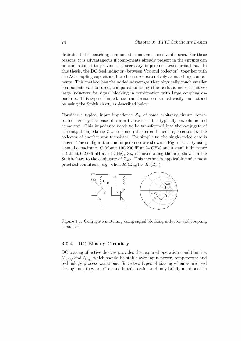
desirable to let matching components consume excessive die area. For thesereasons, it is advantageous if components already present in the circuits canbe dimensioned to provide the necessary impedance transformations. Inthis thesis, the DC feed inductor (between Vcc and collector), together withthe AC coupling capacitors, have been used extensively as matching compo-nents. This method has the added advantage that physically much smallercomponents can be used, compared to using (the perhaps more intuitive)large inductors for signal blocking in combination with large coupling ca-pacitors. This type of impedance transformation is most easily understoodby using the Smith chart, as described below.
Consider a typical input impedance Zin of some arbitrary circuit, repre-sented here by the base of a npn transistor. It is typically low ohmic andcapacitive. This impedance needs to be transformed into the conjugate ofthe output impedance Zout of some other circuit, here represented by thecollector of another npn transistor. For simplicity, the single-ended case isshown. The configuration and impedances are shown in Figure 3.1. By usinga small capacitance C (about 100-200 fF at 24 GHz) and a small inductanceL (about 0.2-0.6 nH at 24 GHz), Zin is moved along the arcs shown in theSmith-chart to the conjugate of Zout. This method is applicable under mostpractical conditions, e.g. when Re(Zout) > Re(Zin).
CL
VccZin
Zout
Zin
Zout*C
L
Figure 3.1: Conjugate matching using signal blocking inductor and couplingcapacitor
3.0.4 DC Biasing Circuitry
DC biasing of active devices provides the required operation condition, i.e.UCEQ and ICQ, which should be stable over input power, temperature andtechnology process variations. Since two types of biasing schemes are usedthroughout, they are discussed in this section and only briefly mentioned in
25
the text concerning each specific RF circuit.
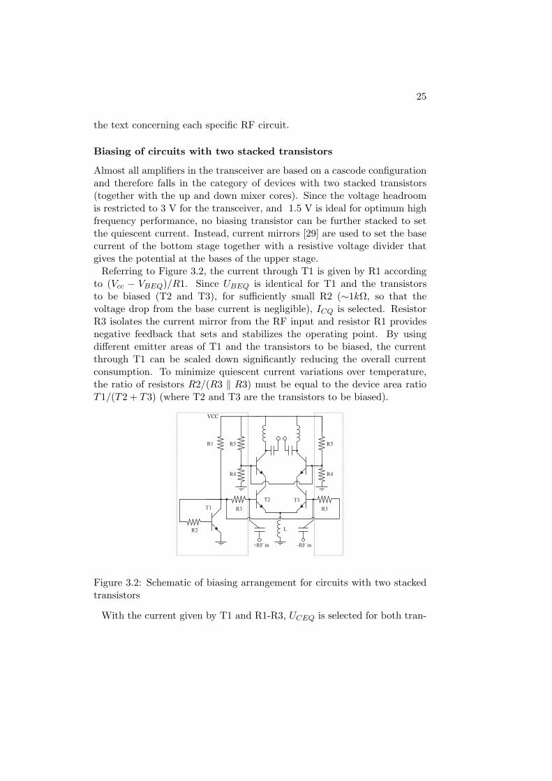
Biasing of circuits with two stacked transistors
Almost all amplifiers in the transceiver are based on a cascode configurationand therefore falls in the category of devices with two stacked transistors(together with the up and down mixer cores). Since the voltage headroomis restricted to 3 V for the transceiver, and 1.5 V is ideal for optimum highfrequency performance, no biasing transistor can be further stacked to setthe quiescent current. Instead, current mirrors [29] are used to set the basecurrent of the bottom stage together with a resistive voltage divider thatgives the potential at the bases of the upper stage.
Referring to Figure 3.2, the current through T1 is given by R1 accordingto (Vcc − VBEQ)/R1. Since UBEQ is identical for T1 and the transistorsto be biased (T2 and T3), for sufficiently small R2 (∼1kΩ, so that thevoltage drop from the base current is negligible), ICQ is selected. ResistorR3 isolates the current mirror from the RF input and resistor R1 providesnegative feedback that sets and stabilizes the operating point. By usingdifferent emitter areas of T1 and the transistors to be biased, the currentthrough T1 can be scaled down significantly reducing the overall currentconsumption. To minimize quiescent current variations over temperature,the ratio of resistors R2/(R3 ‖ R3) must be equal to the device area ratioT1/(T2 + T3) (where T2 and T3 are the transistors to be biased).
+RF in -RF in
VCC
R1
R2
R3 R3
L
R5 R5
R4 R4
T1
T2 T3
Figure 3.2: Schematic of biasing arrangement for circuits with two stackedtransistors
With the current given by T1 and R1-R3, UCEQ is selected for both tran-
26 Chapter 3: RFIC Subcircuits Design
sistor layers by the voltage divider R4 and R5. R4+R5 is first chosen sothat I = V cc/(R4 + R5) is much larger than the base current (for stableoperation), ∼ 10% of ICQ as a rule of thumb, and R5 is then typically 4-5times R4 so that the potential at the base is 2-2.5 V (i.e. 0.7 V above UCEQ).
This way, ICQ and UCEQ of both transistor levels can be easily set. Theinductor L is used as an AC current source to increase common mode re-jection. Further rejection can be obtained by putting a capacitor in parallelwith L, selected to give an anti-resonance at 24 GHz. This however reducesthe bandwidth of the current source.
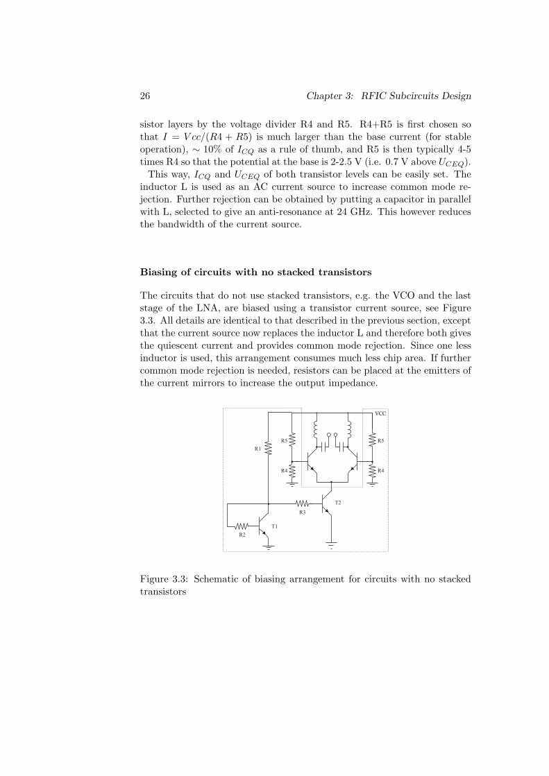
Biasing of circuits with no stacked transistors
The circuits that do not use stacked transistors, e.g. the VCO and the laststage of the LNA, are biased using a transistor current source, see Figure3.3. All details are identical to that described in the previous section, exceptthat the current source now replaces the inductor L and therefore both givesthe quiescent current and provides common mode rejection. Since one lessinductor is used, this arrangement consumes much less chip area. If furthercommon mode rejection is needed, resistors can be placed at the emitters ofthe current mirrors to increase the output impedance.
VCC
R1
R2
R3
R5 R5
R4 R4
T1
T2
Figure 3.3: Schematic of biasing arrangement for circuits with no stackedtransistors
27
3.0.5 Low Noise Amplifier (LNA)
The low noise amplifier (LNA) is the first circuit block in the front-end andmust provide sufficient gain to minimize the impact of mixer noise on theoverall noise figure of the receiver (the well-known gain distribution problem,as quantified in Friis equation 3.1). Since the subharmonic mixers, due tothe higher transistor count compared to standard Gilbert cells, have a highnoise figure (> 15 dB), the LNA needs to provide more than 15 dB of gainwithout itself adding excessive noise.
Ftot = FLNA +FMixer − 1
GLNA+
FBaseband − 1
GLNAGMixer+ . . . (3.1)
For design of amplifiers (LNA, PA, VCO buffers, LO pump amplifiers etc)at high microwave frequencies, techniques to counter the Miller effect (i.e.the feed-back capacitance Cµ transforming into C ′
be = Cµ ∗ (1 − Av), seeFigure 2.4, lowering the input impedance of the active device) is needed.The most common approach to handle this problem is the cascode, i.e. twostacked transistors with the lower in common emitter (CE) and the upperin common base (CB) configuration. Since the upper transistor presentsa load of 1/gm, where gm is the transconductance of the upper transistorand is given by gm = (q/kT ) ∗ ICQ, the voltage gain of the input (lower)transistor is Av = −gm∗Rc = −gm∗(1/gm) = −1. Therefore, the effect of thefeedback capacitor is minimized and contributes only C ′
be = 2∗Cµ to the totalinput capacitance Cπ +C ′
be making the topology suitable for high frequencyusage. Since the transistors are stacked they share DC current. A furtheradvantage of the cascode is increased reverse isolation (S12) making thecircuit extremely stable, especially if used with inductive collector loadingto kill the low frequency gain. On the downside, the stacked transistorsreduces the available voltage headroom (the DC voltage is typically quitelow, < 3 V, at higher RF frequencies) and also increases the noise factor ofthe circuit.
A differential cascode common emitter amplifier configuration was chosenfor the LNA in the receiver. To achieve the necessary gain, the LNA consistsof two cascode stages and one standard differential stage in cascade, seeFigure 3.4. Since the output of the LNA is directly coupled to the emittersof the mixer transistors, there is already a cascode action (i.e. almost novoltage gain at the input transistor) in place and a standard differential pairis therefore sufficient. It was shown through simulations that the conversiongain was higher for a LNA-Mixer conjugate match compared to a using thecascode effect (i.e. the resulting Miller effect was not limiting the amplifier
28 Chapter 3: RFIC Subcircuits Design
gain), and so the DC blocking inductors and AC coupling capacitors in theLNA were sized for a conjugate match. The reduced input impedance ofthe transconductor stage (from the increased input capacitance) also affectsthe sizing of the DC blocking inductor in the second amplifier stage so as tomaintain a good interstage match.
2x0.31 nH
-RF in
2x0.28 nH
2x0.1 pF
2x0.19 nH
+RF in
2x0.1 pF
2x0.1 pF
-RF out
+RF out
Vcc
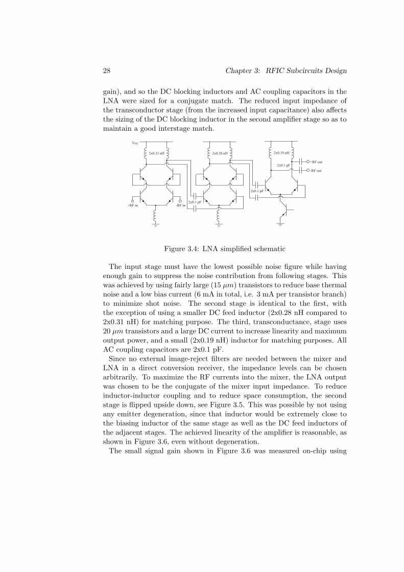
Figure 3.4: LNA simplified schematic
The input stage must have the lowest possible noise figure while havingenough gain to suppress the noise contribution from following stages. Thiswas achieved by using fairly large (15 µm) transistors to reduce base thermalnoise and a low bias current (6 mA in total, i.e. 3 mA per transistor branch)to minimize shot noise. The second stage is identical to the first, withthe exception of using a smaller DC feed inductor (2x0.28 nH compared to2x0.31 nH) for matching purpose. The third, transconductance, stage uses20 µm transistors and a large DC current to increase linearity and maximumoutput power, and a small (2x0.19 nH) inductor for matching purposes. AllAC coupling capacitors are 2x0.1 pF.
Since no external image-reject filters are needed between the mixer andLNA in a direct conversion receiver, the impedance levels can be chosenarbitrarily. To maximize the RF currents into the mixer, the LNA outputwas chosen to be the conjugate of the mixer input impedance. To reduceinductor-inductor coupling and to reduce space consumption, the secondstage is flipped upside down, see Figure 3.5. This was possible by not usingany emitter degeneration, since that inductor would be extremely close tothe biasing inductor of the same stage as well as the DC feed inductors ofthe adjacent stages. The achieved linearity of the amplifier is reasonable, asshown in Figure 3.6, even without degeneration.
The small signal gain shown in Figure 3.6 was measured on-chip using
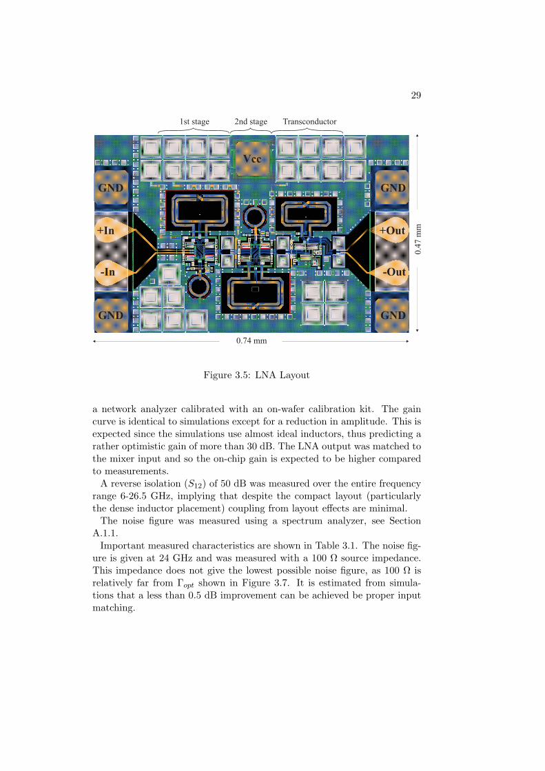
29
+In
-In
+Out
-Out
Vcc
0.74 mm
GND
GND
GND
GND
0.4
7 m
m
1st stage 2nd stage Transconductor
Figure 3.5: LNA Layout
a network analyzer calibrated with an on-wafer calibration kit. The gaincurve is identical to simulations except for a reduction in amplitude. This isexpected since the simulations use almost ideal inductors, thus predicting arather optimistic gain of more than 30 dB. The LNA output was matched tothe mixer input and so the on-chip gain is expected to be higher comparedto measurements.
A reverse isolation (S12) of 50 dB was measured over the entire frequencyrange 6-26.5 GHz, implying that despite the compact layout (particularlythe dense inductor placement) coupling from layout effects are minimal.
The noise figure was measured using a spectrum analyzer, see SectionA.1.1.
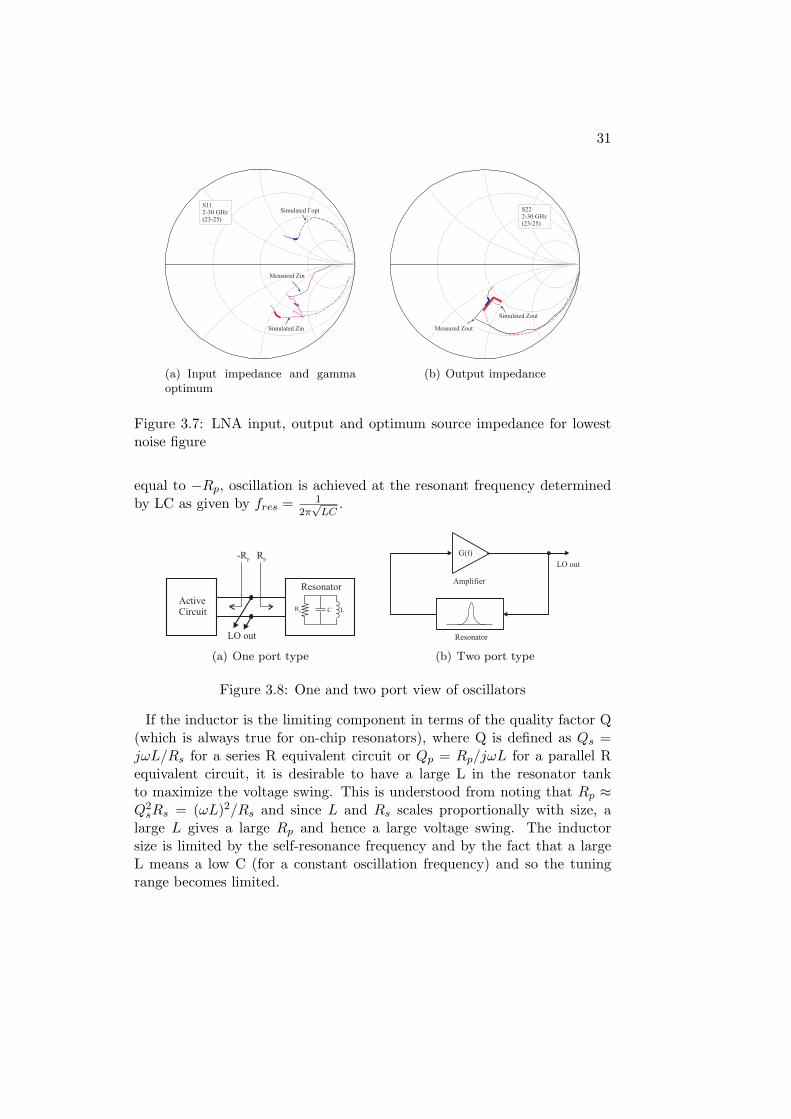
Important measured characteristics are shown in Table 3.1. The noise fig-ure is given at 24 GHz and was measured with a 100 Ω source impedance.This impedance does not give the lowest possible noise figure, as 100 Ω isrelatively far from Γopt shown in Figure 3.7. It is estimated from simula-tions that a less than 0.5 dB improvement can be achieved be proper inputmatching.

30 Chapter 3: RFIC Subcircuits Design
-45 -40 -35 -30 -25 -20 -15 -10 -5 0-30
-25
-20
-15
-10
-5
0
5
10
Input power (dBm)
Ou
tpu
t p
ow
er (
dB
m)
(a) 1 dB compression point
5 10 15 20 250 30
-80
-60
-40
-20
0
20
-100
40
Frequency (GHz)
Gai
n a
nd r
ever
se i
sola
tion(d
B) Simulated gain
Measured gain
Measured isolation
(b) Gain and isolation
Figure 3.6: LNA linearity, gain and reverse isolation
DC Power 73 mA @ 3 V
Gain @ 100Ω 17 dB
Isolation 50 dB
P1dB,in -20 dBm
P1dB,out -4 dBm
3dB gain bandwidth 4 GHz
NF @ 100Ω 6 dB
Table 3.1: LNA measured characteristics
3.0.6 Voltage Controlled Oscillator (VCO)
Frequency translation, i.e. up- and down-conversion, of the informationcarrying signal is performed in the transceiver by multiplying (using mixers)the signal with a high-frequency carrier. The carrier is generated by a localoscillator (LO) whose frequency is determined by a DC voltage, forming avoltage controlled oscillator (VCO).
An oscillator generally consists of a frequency selective network, or res-onator, connected to an amplifier that compensates for losses in the res-onator. Most oscillators can be analyzed using either of two models - thefeedback type (or ”two port”) or negative resistance type (or ”one port”),see Figure 3.8. In the feedback type, oscillation occurs if the loop gain ofthe amplifier-resonator is equal to unity and the total phase shift aroundthe loop is zero (the so called Barkhausen’s critera). For the negative re-sistance type, the resonator can, for a narrow frequency band, be modelledas a parallel RpLC-network and if the active circuit provides an impedance
31
Simulated optG
Simulated Zin
Measured Zin
S112-30 GHz(23-25)
(a) Input impedance and gammaoptimum
Simulated Zout
Measured Zout
S222-30 GHz(23-25)
(b) Output impedance
Figure 3.7: LNA input, output and optimum source impedance for lowestnoise figure
equal to −Rp, oscillation is achieved at the resonant frequency determinedby LC as given by fres = 1
2π√
LC.
ActiveCircuit
Resonator
LO out
Rp-Rp
Rp C L
(a) One port type
G(f)
Amplifier
Resonator
LO out
(b) Two port type
Figure 3.8: One and two port view of oscillators
If the inductor is the limiting component in terms of the quality factor Q(which is always true for on-chip resonators), where Q is defined as Qs =jωL/Rs for a series R equivalent circuit or Qp = Rp/jωL for a parallel Requivalent circuit, it is desirable to have a large L in the resonator tankto maximize the voltage swing. This is understood from noting that Rp ≈Q2
sRs = (ωL)2/Rs and since L and Rs scales proportionally with size, alarge L gives a large Rp and hence a large voltage swing. The inductorsize is limited by the self-resonance frequency and by the fact that a largeL means a low C (for a constant oscillation frequency) and so the tuningrange becomes limited.
32 Chapter 3: RFIC Subcircuits Design
Besides output power, the oscillators phase noise is an important figureof merit. Defined as the noise power within a unit bandwidth, at a certainfrequency offset ∆ω from the carrier ω0, relative to the signal power, itquantifies how large the signal ”skirts” are. Phase noise comes both fromnoise on the VCOs control terminal, from white (thermal and shot) noiseat the carrier frequency, and from up-converted low-frequency (1/f) noise inthe active devices. An often cited equation for describing phase noise (PN)is Leeson’s formula [30]:
PN(∆ω) = 10 log
[
2FkT
Psig
(
1 + (ω0
2Q∆ω)2
)(
1 +∆ω1/f3
|∆ω|
)]
(3.2)
Although the formula contains terms that gives the measured (1/f3) (up-converted 1/f noise), (1/f2) (from white noise) and the broad-band noisefloor components of real oscillators, it contains the empirical fitting param-eter F (determined from measurements) making the formula less suited forpredicting phase noise in the design phase. Furthermore, the formula givesthe boundary between 1/(∆ω)2 and 1/|∆ω|3 regions to be precisely equalto the 1/f corner of the device, which is contradicted by measurements [31].However, the formula is useful for the qualitative information that increas-ing the resonator Q and signal amplitude reduces the phase noise.Concerning phase noise induced by noise on the VCOs control terminal, itcan easily be shown [11] that only low frequency signals affects the oscil-lation frequency. If Vcont is applied at the control terminal, the oscillationfrequency is given by ωout = ω0 + KV COVcont where ω0 is the zero controlvoltage frequency and KV CO is the ”gain” (in rad/s/V) of the VCO. Sincephase is the integral of frequency with respect to time, the VCO outputsignal is given by
vout(t) = A cos
(
ω0t + KV CO
∫ t
−∞Vcont dt
)
(3.3)
For a sinusoidal modulation of the control voltage, Vcont → vcont(t) =Vm cos ωmt, the oscillator output voltage becomes
vout(t) = A cos
(
ω0t +KV CO
ωmVm sinωmt
)
(3.4)
showing that high frequency noise on the control terminal is suppressedby a factor equal to the modulation frequency.
The voltage controlled oscillator (VCO) implemented in this thesis was de-signed using a negative-gm oscillator topology, see Figure 3.9. It consists
33
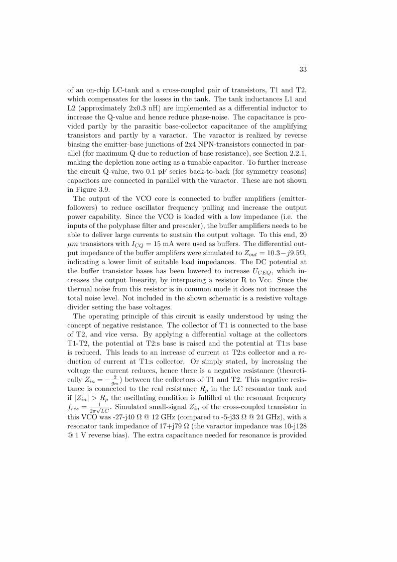
of an on-chip LC-tank and a cross-coupled pair of transistors, T1 and T2,which compensates for the losses in the tank. The tank inductances L1 andL2 (approximately 2x0.3 nH) are implemented as a differential inductor toincrease the Q-value and hence reduce phase-noise. The capacitance is pro-vided partly by the parasitic base-collector capacitance of the amplifyingtransistors and partly by a varactor. The varactor is realized by reversebiasing the emitter-base junctions of 2x4 NPN-transistors connected in par-allel (for maximum Q due to reduction of base resistance), see Section 2.2.1,making the depletion zone acting as a tunable capacitor. To further increasethe circuit Q-value, two 0.1 pF series back-to-back (for symmetry reasons)capacitors are connected in parallel with the varactor. These are not shownin Figure 3.9.
The output of the VCO core is connected to buffer amplifiers (emitter-followers) to reduce oscillator frequency pulling and increase the outputpower capability. Since the VCO is loaded with a low impedance (i.e. theinputs of the polyphase filter and prescaler), the buffer amplifiers needs to beable to deliver large currents to sustain the output voltage. To this end, 20µm transistors with ICQ = 15 mA were used as buffers. The differential out-put impedance of the buffer amplifers were simulated to Zout = 10.3−j9.5Ω,indicating a lower limit of suitable load impedances. The DC potential atthe buffer transistor bases has been lowered to increase UCEQ, which in-creases the output linearity, by interposing a resistor R to Vcc. Since thethermal noise from this resistor is in common mode it does not increase thetotal noise level. Not included in the shown schematic is a resistive voltagedivider setting the base voltages.
The operating principle of this circuit is easily understood by using theconcept of negative resistance. The collector of T1 is connected to the baseof T2, and vice versa. By applying a differential voltage at the collectorsT1-T2, the potential at T2:s base is raised and the potential at T1:s baseis reduced. This leads to an increase of current at T2:s collector and a re-duction of current at T1:s collector. Or simply stated, by increasing thevoltage the current reduces, hence there is a negative resistance (theoreti-cally Zin = − 2
gm) between the collectors of T1 and T2. This negative resis-
tance is connected to the real resistance Rp in the LC resonator tank andif |Zin| > Rp the oscillating condition is fulfilled at the resonant frequencyfres = 1
2π√
LC. Simulated small-signal Zin of the cross-coupled transistor in
this VCO was -27-j40 Ω @ 12 GHz (compared to -5-j33 Ω @ 24 GHz), with aresonator tank impedance of 17+j79 Ω (the varactor impedance was 10-j128@ 1 V reverse bias). The extra capacitance needed for resonance is provided
34 Chapter 3: RFIC Subcircuits Design
VCC
T1T2
C1
VCC
+LO out -LO out
L1L2
(a) Schematic of VCO
+LO
-LO
Polyphase filter
0.95 mm
1.3
mm
+LO
-LO
V control
Vcc VCO
VccPrescaler
+P
rescaler
-Presca
ler
VCOPrescaler
(b) Layout of VCO
Figure 3.9: Schematic and layout of manufactured 12 GHz Voltage Con-trolled Oscillator, with polyphase filter and 1/16 prescaler included in layout
35
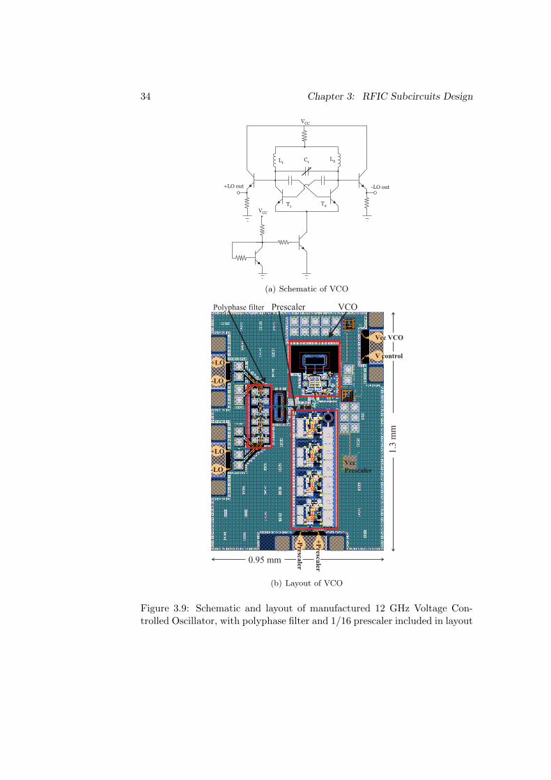
by the buffer amplifiers.
The output power was measured through the polyphase filter and withthe prescaler active to simulate the loading conditions when the VCO isintegrated in the receiver. Compensating for losses in cables, balun andpolyphase filter, the output power is estimated to 0 dBm over the oscil-lating frequency range of 11.8-12.6 GHz. Measured phase noise is below-95 dBc @ 1MHz offset above 12.1 GHz, see Figure 3.10, with increasingphase noise as the reverse bias is reduced (i.e. higher phase noise for lowerfrequencies). It is believed that the measured phase noise is dominated bylow frequency noise pick-up by the voltage probe, which explains the im-provement when the probe was removed (measured at the same frequency).Important measured characteristics are shown in Table 3.2.
As the input impedance of the polyphase filter is low (and capacitive),a parallel 2x0.28 nH differential inductor was interposed between the VCOoutput and filter input. This increases the output voltage of the VCO andalso increases the VCO output linearity.
104
105
106
107
-120
-110
-100
-90
-80
-70
-60
-50
20 dB/Decade
30 dB/Decade
Measurement error
Frequency offset from carrier (Hz)
Ph
ase
no
ise
(dB
c)
Figure 3.10: Measured close-in phase noise of the VCO
3.0.7 Polyphase filter
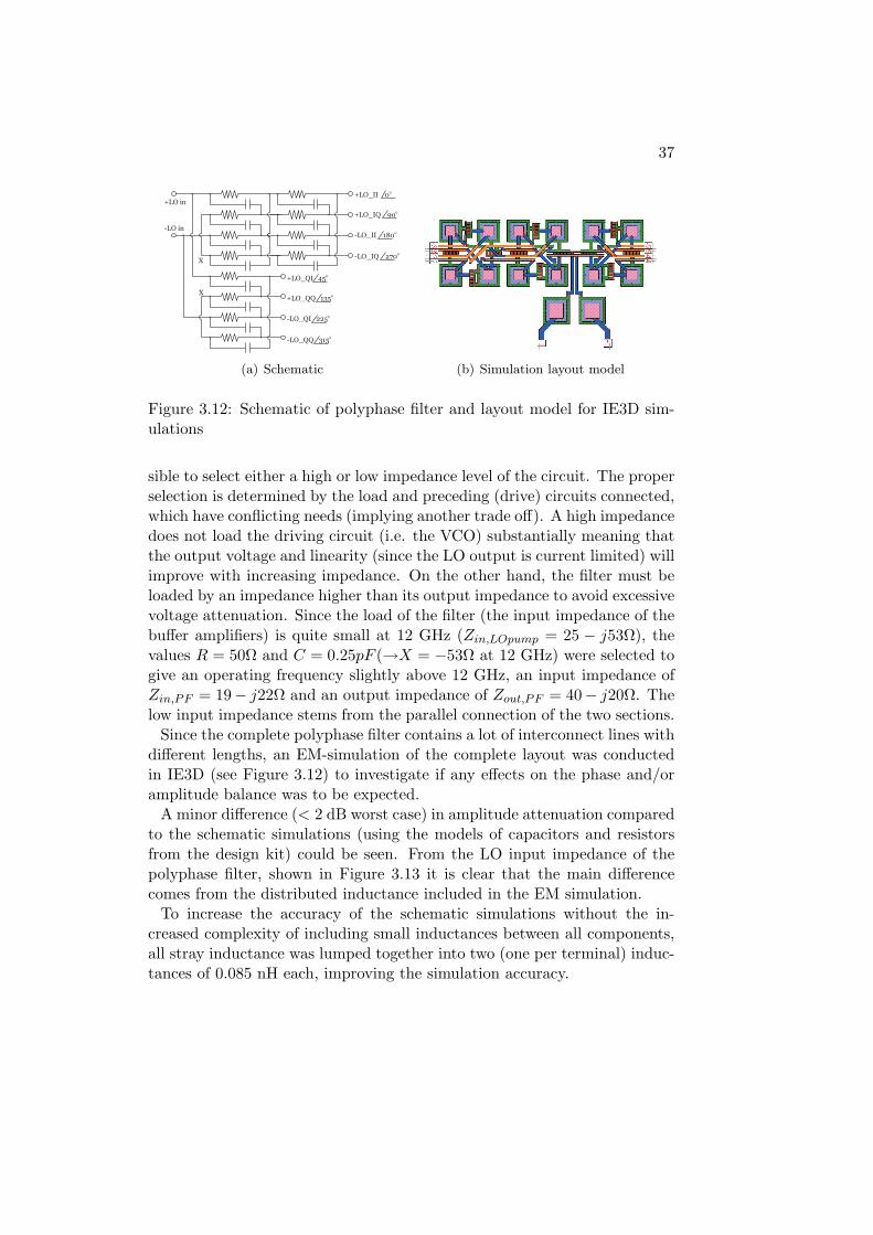
The four necessary LO phases for the I and Q mixers are generated by aRC polyphase filter [16] with two parallel sections. One section contains aneven number of poles (=two) and the other section an odd number of poles(=one) to ensure a 45 shift between the different mixers and a 90 shiftbetween the two switching sections of each mixer, see Figure 3.12.
36 Chapter 3: RFIC Subcircuits Design
11.8 11.9 12.0 12.1 12.2 12.3 12.4 12.5 12.6
-105
-100
-95
-90
-85
11.8 11.9 12.0 12.1 12.2 12.3 12.4 12.5 12.6
-22
-21.5
-21
-20.5
-20
VCO Frequency (GHz)
Ph
ase
no
ise (
dB
c)
Ou
tpu
t p
ow
er
(dB
m)
VCO Frequency (GHz)
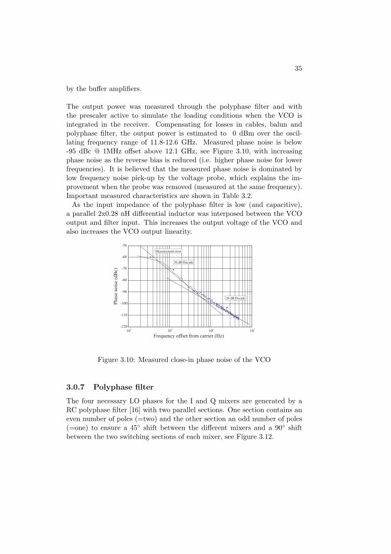
Figure 3.11: Measured output power (bottom) and phase noise at 1 MHzoffset from carrier (top) of VCO
DC Power 36 mA @ 3 V
Output Power 0 dBm
Phase noise @ 1 MHz -95 dBc
Tuning range 11.8 - 12.6 GHz
Output impedance @ 12 GHz 10.3-j9.5 Ω
Table 3.2: VCO characteristics
A polyphase filter has only two degrees of freedom - the number of polesand the impedance level. More poles ensures a higher frequency bandwidthwithin which the output phases are correct, but more poles also means highersignal attenuation. There is therefore a trade off between bandwidth andattenuation. Also, more poles implies a physically larger structure whichconsumes more silicon area (higher cost) and more importantly introducesmore parasitic inductance distributed over the entire network. The mini-mum number, one and two poles, were selected in this work since the rela-tive bandwidth of the 24 GHz band is narrow (< 1%), since the gain of theactive devices is limited at 12 GHz and so the excessive attenuation wouldnecessitate an extra amplifier stage in the LO pump amplifiers resulting inhigher power and area consumption, and since at 12 GHz the interconnectinductance is troublesome enough for one and two poles.
The design frequency of the filter (i.e. where the output phases differs by45) is determined by f = 1/2πRC. For a given frequency it is therefore pos-
37
+LO in
-LO in
+LO_II 00
-LO_II 1800
+LO_IQ 900
-LO_IQ 2700
+LO_QI 450
-LO_QI 2250
+LO_QQ 1350
-LO_QQ 3150
X
X
(a) Schematic (b) Simulation layout model
Figure 3.12: Schematic of polyphase filter and layout model for IE3D sim-ulations
sible to select either a high or low impedance level of the circuit. The properselection is determined by the load and preceding (drive) circuits connected,which have conflicting needs (implying another trade off). A high impedancedoes not load the driving circuit (i.e. the VCO) substantially meaning thatthe output voltage and linearity (since the LO output is current limited) willimprove with increasing impedance. On the other hand, the filter must beloaded by an impedance higher than its output impedance to avoid excessivevoltage attenuation. Since the load of the filter (the input impedance of thebuffer amplifiers) is quite small at 12 GHz (Zin,LOpump = 25 − j53Ω), thevalues R = 50Ω and C = 0.25pF (→X = −53Ω at 12 GHz) were selected togive an operating frequency slightly above 12 GHz, an input impedance ofZin,PF = 19− j22Ω and an output impedance of Zout,PF = 40− j20Ω. Thelow input impedance stems from the parallel connection of the two sections.
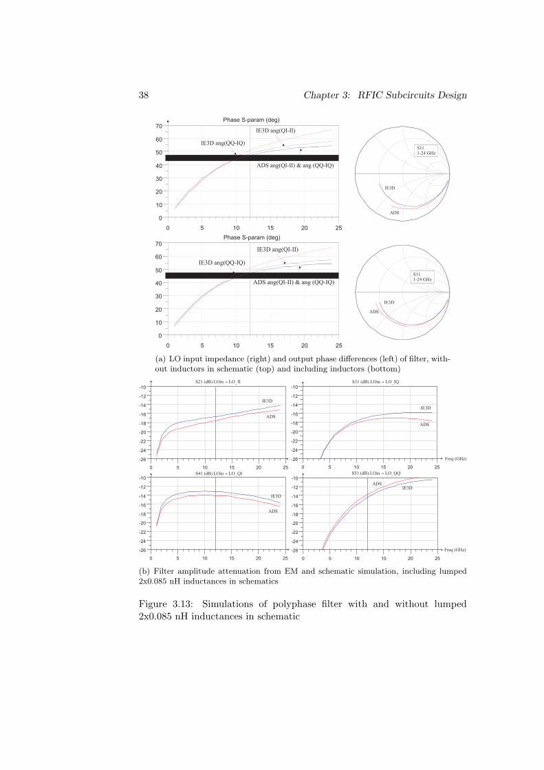
Since the complete polyphase filter contains a lot of interconnect lines withdifferent lengths, an EM-simulation of the complete layout was conductedin IE3D (see Figure 3.12) to investigate if any effects on the phase and/oramplitude balance was to be expected.
A minor difference (< 2 dB worst case) in amplitude attenuation comparedto the schematic simulations (using the models of capacitors and resistorsfrom the design kit) could be seen. From the LO input impedance of thepolyphase filter, shown in Figure 3.13 it is clear that the main differencecomes from the distributed inductance included in the EM simulation.
To increase the accuracy of the schematic simulations without the in-creased complexity of including small inductances between all components,all stray inductance was lumped together into two (one per terminal) induc-tances of 0.085 nH each, improving the simulation accuracy.
38 Chapter 3: RFIC Subcircuits Design
5 10 15 200 25
10
20
30
40
50
60
0
70
IE3D ang(QQ-IQ)
Phase S-param (deg)
IE3D ang(QI-II)
ADS ang(QI-II) & ang (QQ-IQ)
IE3D
ADS
S111-24 GHz
5 10 15 200 25
10
20
30
40
50
60
0
70
S111-24 GHz
IE3D
ADS
IE3D ang(QQ-IQ)
Phase S-param (deg)
IE3D ang(QI-II)
ADS ang(QI-II) & ang (QQ-IQ)
(a) LO input impedance (right) and output phase differences (left) of filter, with-out inductors in schematic (top) and including inductors (bottom)
5 10 15 200 25
-24
-22
-20
-18
-16
-14
-12
-26
-10
5 10 15 200 25
-24
-22
-20
-18
-16
-14
-12
-26
-10
5 10 15 200 25
-24
-22
-20
-18
-16
-14
-12
-26
-10
5 10 15 200 25
-24
-22
-20
-18
-16
-14
-12
-26
-10
S21 (dB) LOin LO_IIg
S41 (dB) LOin LO_QIg
S31 (dB) LOin LO_IQg
S51 (dB) LOin LO_QQg
ADS
IE3D
ADS
IE3D
ADS
IE3D
ADSIE3D
Freq (GHz)
Freq (GHz)
(b) Filter amplitude attenuation from EM and schematic simulation, including lumped2x0.085 nH inductances in schematics
Figure 3.13: Simulations of polyphase filter with and without lumped2x0.085 nH inductances in schematic
39
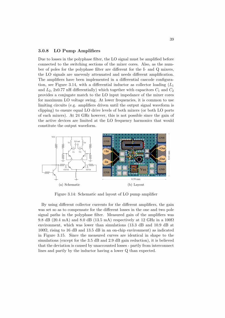
3.0.8 LO Pump Amplifiers
Due to losses in the polyphase filter, the LO signal must be amplified beforeconnected to the switching sections of the mixer cores. Also, as the num-ber of poles for the polyphase filter are different for the I- and Q mixers,the LO signals are unevenly attenuated and needs different amplification.The amplifiers have been implemented in a differential cascode configura-tion, see Figure 3.14, with a differential inductor as collector loading (L1
and L2, 2x0.77 nH differentially) which together with capacitors C1 and C2
provides a conjugate match to the LO input impedance of the mixer coresfor maximum LO voltage swing. At lower frequencies, it is common to uselimiting circuits (e.g. amplifiers driven until the output signal waveform isclipping) to ensure equal LO drive levels of both mixers (or both LO portsof each mixers). At 24 GHz however, this is not possible since the gain ofthe active devices are limited at the LO frequency harmonics that wouldconstitute the output waveform.
+LO in -LO in
LO out+ -L1 L2
VCC
C1 C2
(a) Schematic
+In
-In
Vcc
0.59 mm
GND
GND
0.4
1 m
m
+Out
-Out
GND
GND
(b) Layout
Figure 3.14: Schematic and layout of LO pump amplifier
By using different collector currents for the different amplifiers, the gainwas set so as to compensate for the different losses in the one and two polesignal paths in the polyphase filter. Measured gain of the amplifiers was9.8 dB (20.4 mA) and 8.0 dB (13.5 mA) respectively at 12 GHz in a 100Ωenvironment, which was lower than simulations (13.3 dB and 10.9 dB at100Ω, rising to 16 dB and 13.5 dB in an on-chip environment) as indicatedin Figure 3.15. Since the measured curves are identical in shape to thesimulations (except for the 3.5 dB and 2.9 dB gain reduction), it is believedthat the deviation is caused by unaccounted losses - partly from interconnectlines and partly by the inductor having a lower Q than expected.
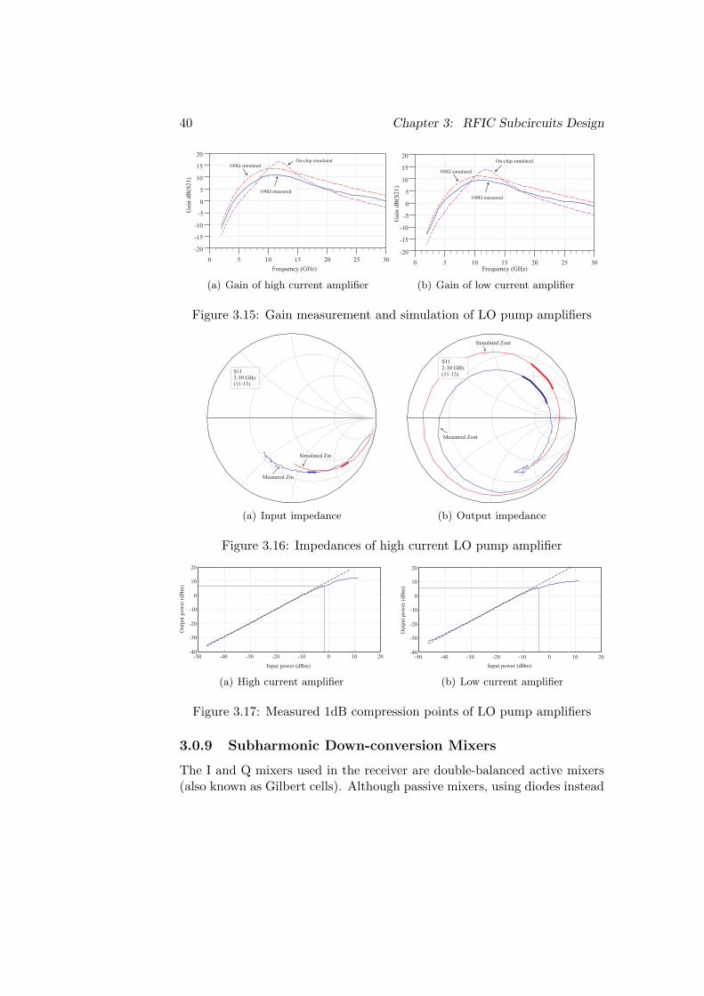
40 Chapter 3: RFIC Subcircuits Design
5 10 15 20 250 30
-15
-10
-5
0
5
10
15
-20
20
Gai
n d
B(S
21
)
Frequency (GHz)
100 simulatedWOn-chip simulated
100 measuredW
(a) Gain of high current amplifier
5 10 15 20 250 30
-15
-10
-5
0
5
10
15
-20
20
Gai
n d
B(S
21
)
Frequency (GHz)
100 simulatedW
On-chip simulated
100 measuredW
(b) Gain of low current amplifier
Figure 3.15: Gain measurement and simulation of LO pump amplifiers
Simulated Zin
S112-30 GHz(11-13)
Measured Zin
(a) Input impedance
S112-30 GHz(11-13)
Simulated Zout
Measured Zout
(b) Output impedance
Figure 3.16: Impedances of high current LO pump amplifier
-50 -40 -30 -20 -10 0 10 20-40
-30
-20
-10
0
10
20
Input power (dBm)
Ou
tpu
t p
ow
er (
dB
m)
(a) High current amplifier
-50 -40 -30 -20 -10 0 10 20-40
-30
-20
-10
0
10
20
Input power (dBm)
Ou
tpu
t p
ow
er (
dB
m)
(b) Low current amplifier
Figure 3.17: Measured 1dB compression points of LO pump amplifiers
3.0.9 Subharmonic Down-conversion Mixers
The I and Q mixers used in the receiver are double-balanced active mixers(also known as Gilbert cells). Although passive mixers, using diodes instead
41
5 10 15 20 250 30
-50
-40
-30
-20
-10
-60
0
Rev
erse
Iso
lati
on
(d
B)
Frequency (GHz)
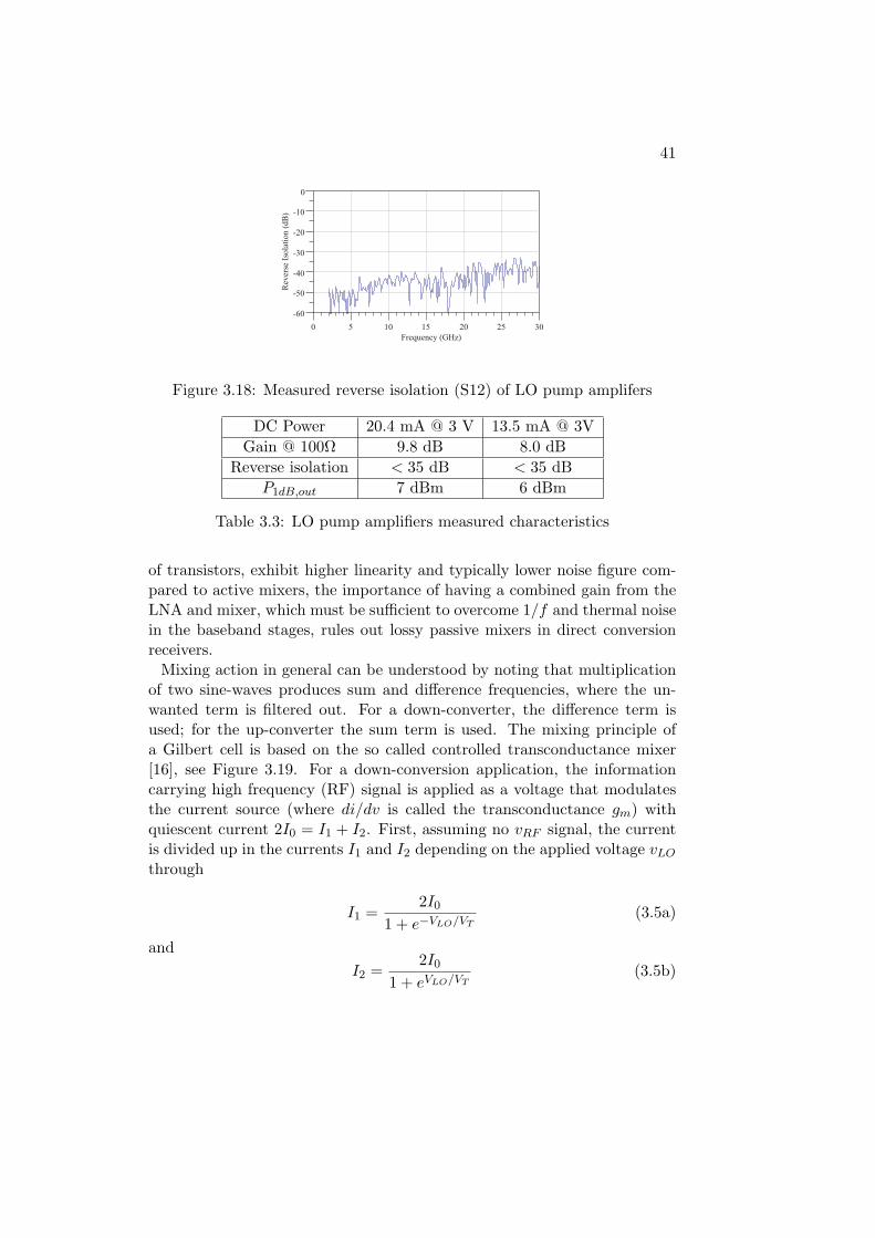
Figure 3.18: Measured reverse isolation (S12) of LO pump amplifers
DC Power 20.4 mA @ 3 V 13.5 mA @ 3V
Gain @ 100Ω 9.8 dB 8.0 dB
Reverse isolation < 35 dB < 35 dB
P1dB,out 7 dBm 6 dBm
Table 3.3: LO pump amplifiers measured characteristics
of transistors, exhibit higher linearity and typically lower noise figure com-pared to active mixers, the importance of having a combined gain from theLNA and mixer, which must be sufficient to overcome 1/f and thermal noisein the baseband stages, rules out lossy passive mixers in direct conversionreceivers.
Mixing action in general can be understood by noting that multiplicationof two sine-waves produces sum and difference frequencies, where the un-wanted term is filtered out. For a down-converter, the difference term isused; for the up-converter the sum term is used. The mixing principle ofa Gilbert cell is based on the so called controlled transconductance mixer[16], see Figure 3.19. For a down-conversion application, the informationcarrying high frequency (RF) signal is applied as a voltage that modulatesthe current source (where di/dv is called the transconductance gm) withquiescent current 2I0 = I1 + I2. First, assuming no vRF signal, the currentis divided up in the currents I1 and I2 depending on the applied voltage vLO
through
I1 =2I0
1 + e−VLO/VT(3.5a)
and
I2 =2I0
1 + eVLO/VT(3.5b)
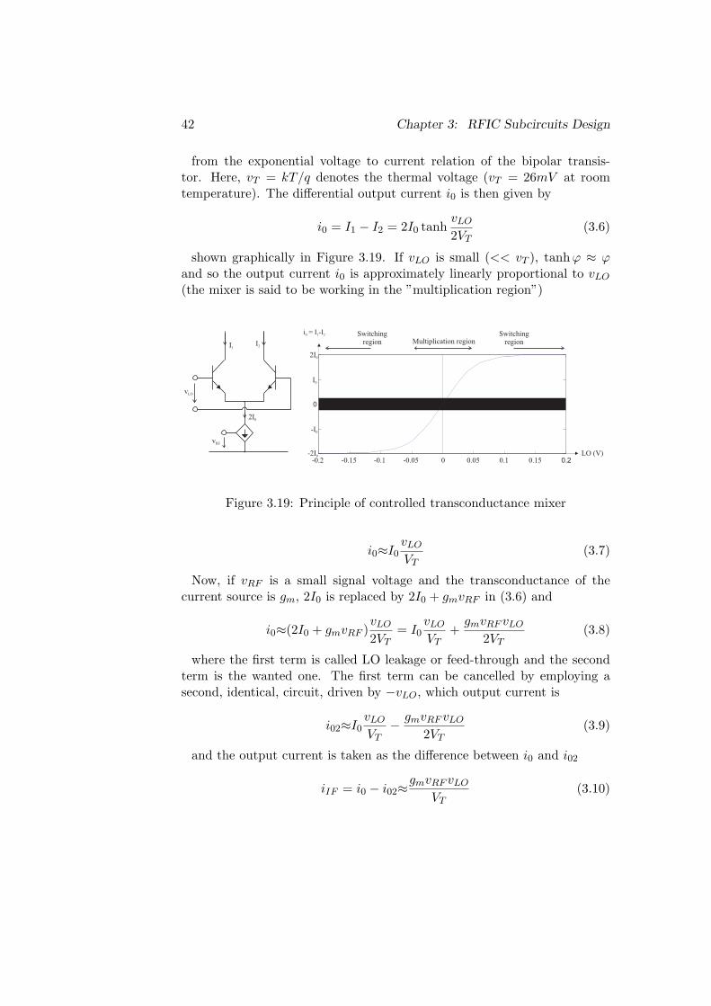
42 Chapter 3: RFIC Subcircuits Design
from the exponential voltage to current relation of the bipolar transis-tor. Here, vT = kT/q denotes the thermal voltage (vT = 26mV at roomtemperature). The differential output current i0 is then given by
i0 = I1 − I2 = 2I0 tanhvLO
2VT(3.6)
shown graphically in Figure 3.19. If vLO is small (<< vT ), tanhϕ ≈ ϕand so the output current i0 is approximately linearly proportional to vLO
(the mixer is said to be working in the ”multiplication region”)
vLO
vRF
I1I2
2I0
-0.2 -0.15 -0.1 -0.05 0 0.05 0.1 0.15 0.2-2I0
-I0
0
I0
2I0
LO (V)
i = I -I0 1 2
Multiplication regionSwitching
regionSwitching
region
Figure 3.19: Principle of controlled transconductance mixer
i0≈I0
vLO
VT(3.7)
Now, if vRF is a small signal voltage and the transconductance of thecurrent source is gm, 2I0 is replaced by 2I0 + gmvRF in (3.6) and
i0≈(2I0 + gmvRF )vLO
2VT= I0
vLO
VT+
gmvRF vLO
2VT(3.8)
where the first term is called LO leakage or feed-through and the secondterm is the wanted one. The first term can be cancelled by employing asecond, identical, circuit, driven by −vLO, which output current is
i02≈I0
vLO
VT− gmvRF vLO
2VT(3.9)
and the output current is taken as the difference between i0 and i02
iIF = i0 − i02≈gmvRF vLO
VT(3.10)
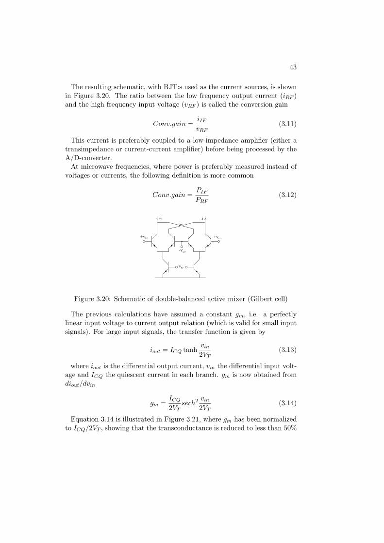
43
The resulting schematic, with BJT:s used as the current sources, is shownin Figure 3.20. The ratio between the low frequency output current (iRF )and the high frequency input voltage (vRF ) is called the conversion gain
Conv.gain =iIF
vRF(3.11)
This current is preferably coupled to a low-impedance amplifier (either atransimpedance or current-current amplifier) before being processed by theA/D-converter.
At microwave frequencies, where power is preferably measured instead ofvoltages or currents, the following definition is more common
Conv.gain =PIF
PRF(3.12)
+vLO
vRF
+vLO
-vLO
+i -i
Figure 3.20: Schematic of double-balanced active mixer (Gilbert cell)
The previous calculations have assumed a constant gm, i.e. a perfectlylinear input voltage to current output relation (which is valid for small inputsignals). For large input signals, the transfer function is given by
iout = ICQ tanhvin
2VT(3.13)
where iout is the differential output current, vin the differential input volt-age and ICQ the quiescent current in each branch. gm is now obtained fromdiout/dvin
gm =ICQ
2VTsech2 vin
2VT(3.14)
Equation 3.14 is illustrated in Figure 3.21, where gm has been normalizedto ICQ/2VT , showing that the transconductance is reduced to less than 50%

44 Chapter 3: RFIC Subcircuits Design
of the peak value (for vin = 0) at input signals of 50 mV (amplitude). Byusing several differential pairs in parallel, with different emitter sizes of thetransistors, it is possible to obtain a flatter gm = gm(vin) dependence (fromthe so called ”multi-tanh principle” [32]). This however also increases thenoise figure of the circuit due to the larger transistor count. Other means toincrease the linearity is to use emitter degeneration of the differential pair.In some cases, linearity can be limited by saturation of the switching quad.This problem can be reduced by using inductive collector loading (at leastfor the up-conversion) instead of resistive to enable larger voltage swings.
-0.2 -0.15 -0.1 -0.05 0 0.05 0.1 0.150
0.5
1
Norm
aliz
ed t
ransc
onduct
ance
, gm
Input rf voltage (V)
Figure 3.21: Transconductance gm of RF input stage for large signals
Ideally, Gilbert cells are used as ”switching modulators”, i.e. vLO is drivenas a large square wave hard-switching the LO transistors (switch quad) al-ternately on and off. The reason for this is to maximize the signal-to-noiseratio at the output (i.e. minimizing the noise figure). It can be shownthat the noise behavior of switching modulators are always much betterthan non-switching (multiplying) types. Although not trivial to derive, itcan intuitively be understood from the following: The output signal levelis increased with large vLO levels as seen from Eq. (3.10), up to a certainlevel (about 100 mV peak, see Figure 3.19). At the same time, the noisefrom the switching transistors are kept to a minimum since half of them arealternately turned off (and are therefore not contributing any noise). Atmicrowave frequencies, and especially when operating close to the transis-tors fT (as in this thesis), two problems arises. First, it is not possible togenerate a square wave for the LO voltage as the active devices have almostno gain at the necessary harmonics that comprises the square wave. There-fore, a large sine wave is used instead. The amplitude of the sine needs
45
to be large partly to hard-switch the transistors but also to minimize therise-time to reach the on-off stages (during which no transistors are off andall transistors are therefore contributing noise). If the LO voltage is madetoo large, high-current effects in the bases of the BJT:s can actually reducethe switching speed and cause an increase of LO feed-through. Typically100-300 mV peak is a recommended LO level in the literature [16]. The sec-ond problem of operating at high frequencies is that the ∼100-300 mV needsto be applied to the intrinsic base-emitter junction of the active device (thecapacitor Cπ), so the voltage at the external transistor terminals needs to bemuch bigger since most of it will be across the base resistance rb. Becausethe input impedance of the LO transistors are low, a lot of power needs tobe dissipated to obtain the necessary switching voltage level.
The 24 GHz down-conversion mixers used in the receiver are based on a mod-ified Gilbert cell topology [33] with two stacked switching sectors (”three-level multiplier” [34]) pumped with 12 GHz LO signals 90 out of phase.Since the Gilbert cell can be thought of as a multiplying circuit, the subhar-monic mixing action can be understood from noting that the extra switchingstage adds another LO multiplication term, see Eq. (3.15),
vIF (t) = A cos(ωRF t+ϕ) sin(ωLOt) cos(ωLOt) = B cos(ωRF t+ϕ) sin(2ωLOt)(3.15)
meaning that the VCO can operate at half the RF frequency [33]. Thishas several advantages for the VCO design (see Section 3.0.6), but moreimportantly for the system level performance (see Section 2.1).
As the voltage headroom for the receiver is limited to 3V, only two transis-tors can be stacked for optimum high frequency performance. Therefore, thetransconductance amplifier (differential pair) that usually forms the bottomof the mixer has been folded and is biased in parallel with the switchingstages, see Figure 3.22.
The RF output current of the differential pair is coupled to the emittersof the first switching sector through capacitors C1 and C2. The inductorsL1 and L2, implemented as a differential inductor, are large and acts ascurrent sources for signal frequencies. Inductors L3 and L4 (also realized asa differential inductor) and capacitors C1 and C2 transforms the low inputimpedance of the bottom switching section into the conjugate of the outputof the transconductor, resulting in higher RF currents and ultimately higherconversion gain. Inductors L5 and L6 (one differential inductor) introducesfeedback that increases the input impedance and linearity but lowers the
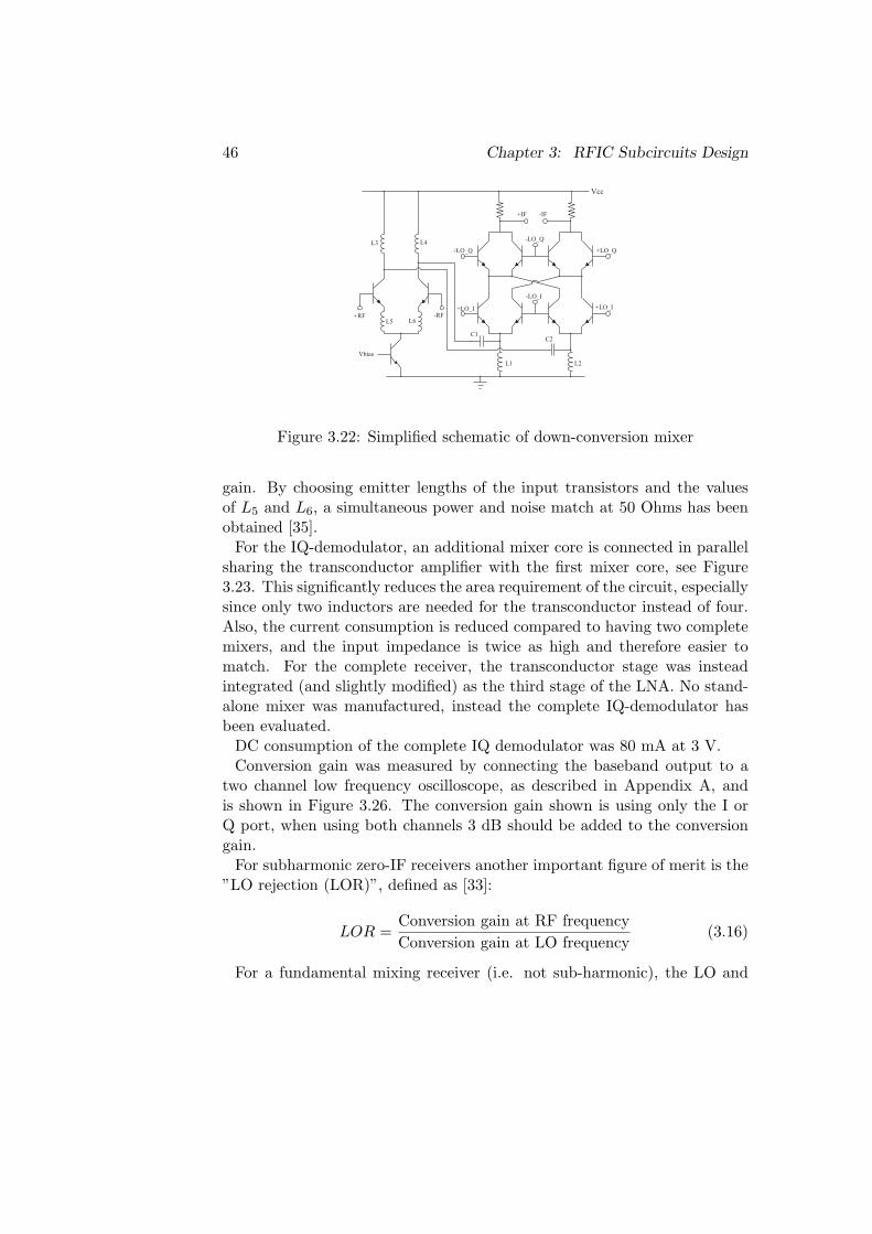
46 Chapter 3: RFIC Subcircuits Design
+IF -IF
+LO_Q +LO_Q
+LO_I +LO_I
-LO_I
-LO_Q
+RF -RF
Vcc
L1 L2
L3 L4
C1C2
L5 L6
Vbias
Figure 3.22: Simplified schematic of down-conversion mixer
gain. By choosing emitter lengths of the input transistors and the valuesof L5 and L6, a simultaneous power and noise match at 50 Ohms has beenobtained [35].
For the IQ-demodulator, an additional mixer core is connected in parallelsharing the transconductor amplifier with the first mixer core, see Figure3.23. This significantly reduces the area requirement of the circuit, especiallysince only two inductors are needed for the transconductor instead of four.Also, the current consumption is reduced compared to having two completemixers, and the input impedance is twice as high and therefore easier tomatch. For the complete receiver, the transconductor stage was insteadintegrated (and slightly modified) as the third stage of the LNA. No stand-alone mixer was manufactured, instead the complete IQ-demodulator hasbeen evaluated.
DC consumption of the complete IQ demodulator was 80 mA at 3 V.Conversion gain was measured by connecting the baseband output to a
two channel low frequency oscilloscope, as described in Appendix A, andis shown in Figure 3.26. The conversion gain shown is using only the I orQ port, when using both channels 3 dB should be added to the conversiongain.
For subharmonic zero-IF receivers another important figure of merit is the”LO rejection (LOR)”, defined as [33]:
LOR =Conversion gain at RF frequency
Conversion gain at LO frequency(3.16)
For a fundamental mixing receiver (i.e. not sub-harmonic), the LO and
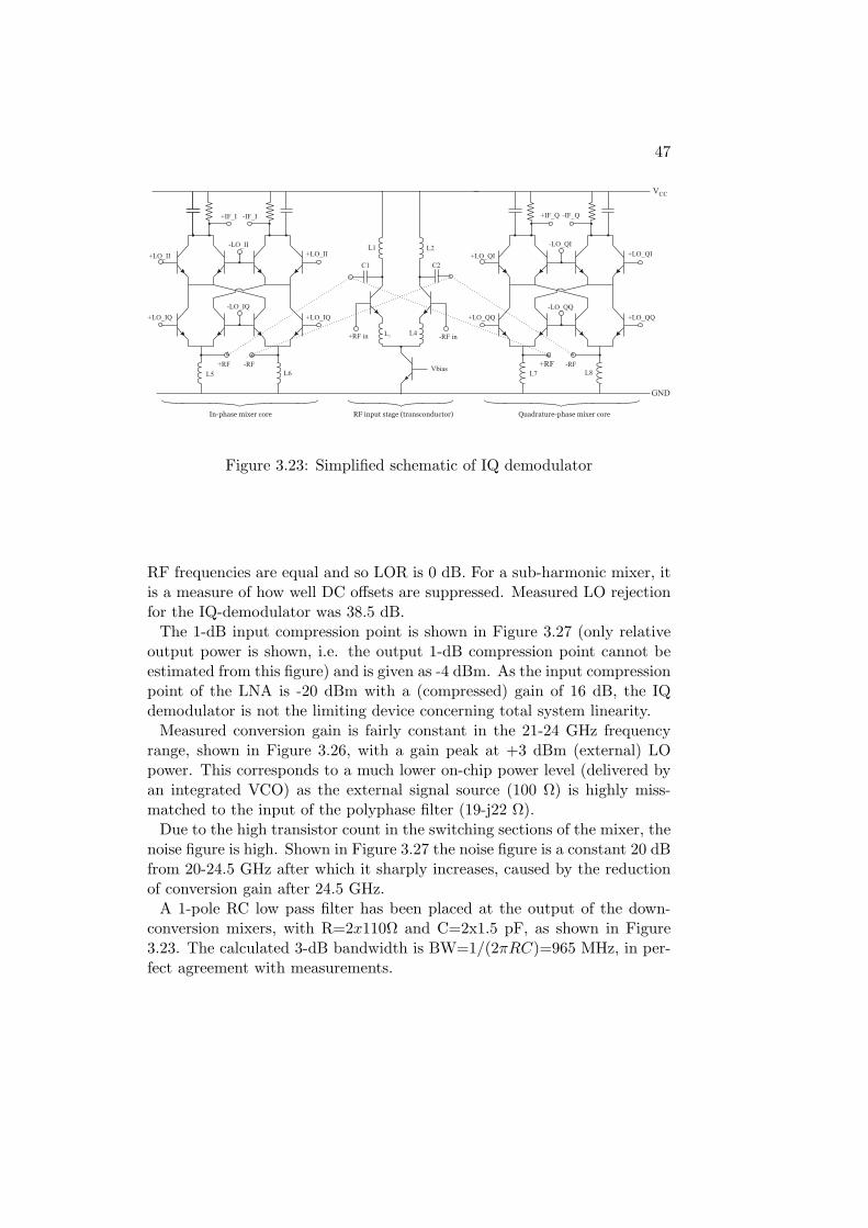
47
VCC
+IF_I -IF_I
+LO_II +LO_II
+LO_IQ +LO_IQ
-LO_IQ
-LO_II
+IF_Q -IF_Q
+LO_QI +LO_QI
+LO_QQ +LO_QQ
-LO_QQ
-LO_QI
In-phase mixer core Quadrature-phase mixer core
+RF -RF +RF -RF
RF input stage (transconductor)
GND
L5 L6 L7 L8
L1 L2
L3L4+RF in -RF in
C1 C2
Vbias
Figure 3.23: Simplified schematic of IQ demodulator
RF frequencies are equal and so LOR is 0 dB. For a sub-harmonic mixer, itis a measure of how well DC offsets are suppressed. Measured LO rejectionfor the IQ-demodulator was 38.5 dB.
The 1-dB input compression point is shown in Figure 3.27 (only relativeoutput power is shown, i.e. the output 1-dB compression point cannot beestimated from this figure) and is given as -4 dBm. As the input compressionpoint of the LNA is -20 dBm with a (compressed) gain of 16 dB, the IQdemodulator is not the limiting device concerning total system linearity.
Measured conversion gain is fairly constant in the 21-24 GHz frequencyrange, shown in Figure 3.26, with a gain peak at +3 dBm (external) LOpower. This corresponds to a much lower on-chip power level (delivered byan integrated VCO) as the external signal source (100 Ω) is highly miss-matched to the input of the polyphase filter (19-j22 Ω).
Due to the high transistor count in the switching sections of the mixer, thenoise figure is high. Shown in Figure 3.27 the noise figure is a constant 20 dBfrom 20-24.5 GHz after which it sharply increases, caused by the reductionof conversion gain after 24.5 GHz.
A 1-pole RC low pass filter has been placed at the output of the down-conversion mixers, with R=2x110Ω and C=2x1.5 pF, as shown in Figure3.23. The calculated 3-dB bandwidth is BW=1/(2πRC)=965 MHz, in per-fect agreement with measurements.
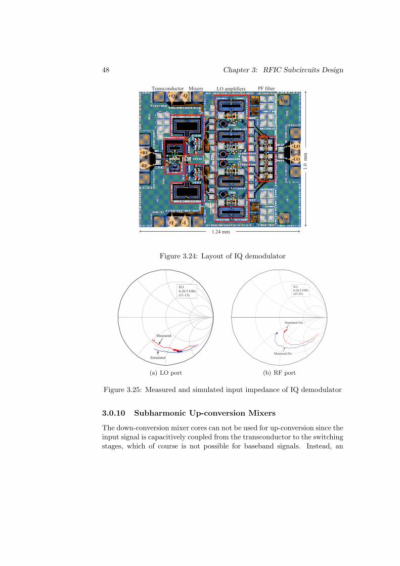
48 Chapter 3: RFIC Subcircuits Design
Vcc
Vcc
+RF
-RF
+Q -Q
+I -I
+LO
-LO
LO amplifiers PF filter
1.24 mm
1.0
m
m
Vcc
Vcc
MixersTransconductor
Figure 3.24: Layout of IQ demodulator
S116-26.5 GHz(11-13)
Measured
Simulated
(a) LO port
Simulated Zin
Measured Zin
S116-26.5 GHz(23-25)
(b) RF port
Figure 3.25: Measured and simulated input impedance of IQ demodulator
3.0.10 Subharmonic Up-conversion Mixers
The down-conversion mixer cores can not be used for up-conversion since theinput signal is capacitively coupled from the transconductor to the switchingstages, which of course is not possible for baseband signals. Instead, an
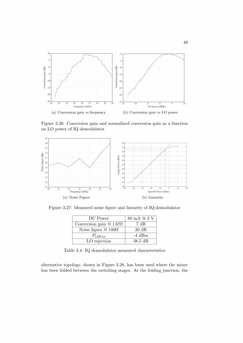
49
12 14 16 18 20 22 24 26 28-25
-20
-15
-10
-5
0
5
10
Conver
sion g
ain (
dB
)
Frequency (GHz)
(a) Conversion gain vs frequency
-15 -10 -5 0 5 10-35
-30
-25
-20
-15
-10
-5
0
LO power (dBm)
Conver
sion g
ain (
dB
)
(b) Conversion gain vs LO power
Figure 3.26: Conversion gain and normalized conversion gain as a functionon LO power of IQ demodulator
20 21 22 23 24 25 2615
16
17
18
19
20
21
22
23
24
25
Frequency (GHz)
Nois
e F
igure
(dB
)
(a) Noise Figure
-50 -40 -30 -20 -10 0 10 20-60
-55
-50
-45
-40
-35
-30
-25
-20
-15
-10
Input RF Power (dBm)
Ou
tpu
t P
ow
er (
dB
m)
(b) Linearity
Figure 3.27: Measured noise figure and linearity of IQ-demodulator
DC Power 80 mA @ 3 V
Conversion gain @ 1MΩ 7 dB
Noise figure @ 100Ω 20 dB
P1dB,in -4 dBm
LO rejection 38.5 dB
Table 3.4: IQ demodulator measured characteristics
alternative topology, shown in Figure 3.28, has been used where the mixerhas been folded between the switching stages. At the folding junction, the
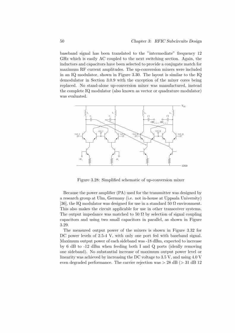
50 Chapter 3: RFIC Subcircuits Design
baseband signal has been translated to the ”intermediate” frequency 12GHz which is easily AC coupled to the next switching section. Again, theinductors and capacitors have been selected to provide a conjugate match formaximum RF current amplitudes. The up-conversion mixers were includedin an IQ modulator, shown in Figure 3.30. The layout is similar to the IQdemodulator in Section 3.0.9 with the exception of the mixer cores beingreplaced. No stand-alone up-conversion mixer was manufactured, insteadthe complete IQ modulator (also known as vector or quadrature modulator)was evaluated.
+LO_I +LO_I
-LO_I
+IFin -IFin
+LO_Q +LO_Q
-LO_Q
VCC
GND
+RFo u t -RFo u t
L1L2 L3
L4
C1C2 C3 C4
Figure 3.28: Simplified schematic of up-conversion mixer
Because the power amplifier (PA) used for the transmitter was designed bya research group at Ulm, Germany (i.e. not in-house at Uppsala University)[36], the IQ modulator was designed for use in a standard 50 Ω environment.This also makes the circuit applicable for use in other transceiver systems.The output impedance was matched to 50 Ω by selection of signal couplingcapacitors and using two small capacitors in parallel, as shown in Figure3.29.
The measured output power of the mixers is shown in Figure 3.32 forDC power levels of 2.5-4 V, with only one port fed with baseband signal.Maximum output power of each sideband was -18 dBm, expected to increaseby 6 dB to -12 dBm when feeding both I and Q ports (ideally removingone sideband). No substantial increase of maximum output power level orlinearity was achieved by increasing the DC voltage to 3.5 V, and using 4.0 Veven degraded performance. The carrier rejection was > 28 dB (> 31 dB 12
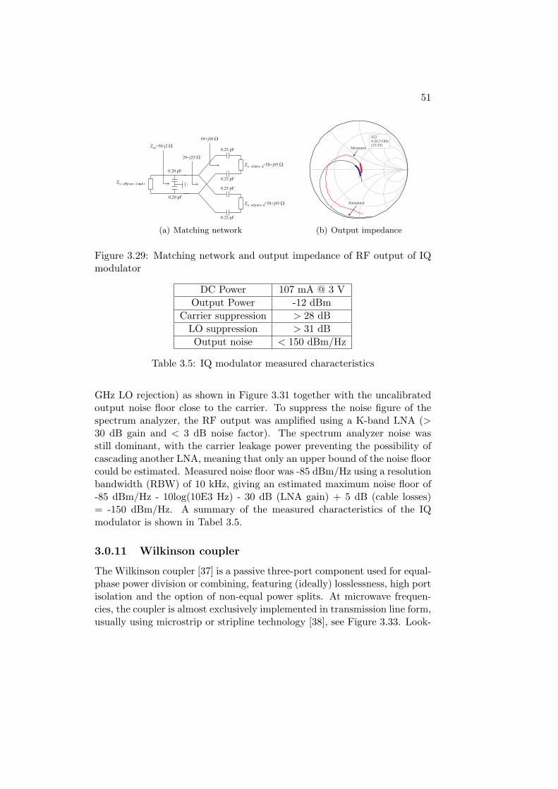
51
Zo u tI-mix er=58+j95 W
0.25 pF
0.25 pF
59+j50 W
Zo u tQ-mix er=58+j95 W
0.25 pF
0.25 pF
0.20 pF
0.20 pF
29+j25 W
Zin=50-j2 W
Zo u tIQ-mo d u lato r
(a) Matching network
Simulated
S226-26.5 GHz(23-25)
Measured
(b) Output impedance
Figure 3.29: Matching network and output impedance of RF output of IQmodulator
DC Power 107 mA @ 3 V
Output Power -12 dBm
Carrier suppression > 28 dB
LO suppression > 31 dB
Output noise < 150 dBm/Hz
Table 3.5: IQ modulator measured characteristics
GHz LO rejection) as shown in Figure 3.31 together with the uncalibratedoutput noise floor close to the carrier. To suppress the noise figure of thespectrum analyzer, the RF output was amplified using a K-band LNA (>30 dB gain and < 3 dB noise factor). The spectrum analyzer noise wasstill dominant, with the carrier leakage power preventing the possibility ofcascading another LNA, meaning that only an upper bound of the noise floorcould be estimated. Measured noise floor was -85 dBm/Hz using a resolutionbandwidth (RBW) of 10 kHz, giving an estimated maximum noise floor of-85 dBm/Hz - 10log(10E3 Hz) - 30 dB (LNA gain) + 5 dB (cable losses)= -150 dBm/Hz. A summary of the measured characteristics of the IQmodulator is shown in Tabel 3.5.
3.0.11 Wilkinson coupler
The Wilkinson coupler [37] is a passive three-port component used for equal-phase power division or combining, featuring (ideally) losslessness, high portisolation and the option of non-equal power splits. At microwave frequen-cies, the coupler is almost exclusively implemented in transmission line form,usually using microstrip or stripline technology [38], see Figure 3.33. Look-
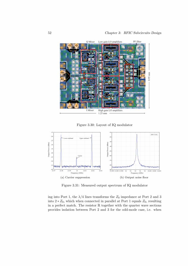
52 Chapter 3: RFIC Subcircuits Design
Vcc
Vcc
+RF
-RF
+Q -Q
+I -I
+LO
-LO
Q Mixer
I Mixer
Low gain LO amplifiers
High gain LO amplifiers
PF filter
1.25 mm
0.9
5 m
m
Figure 3.30: Layout of IQ modulator
23.97 23.98 23.99 24 24.01 24.02 24.03-60
-55
-50
-45
-40
-35
-30
-25
-20
-15
Upper sidebandLower sideband
Carrier
Frequency (GHz)
Outp
ut
Pow
er (
dB
m)
(a) Carrier suppression
23.999 23.999 23.999 24 24 24 24 24 24.001 24.001 24.001-90
-80
-70
-60
-50
-40
-30
-20
-10
RBW 10 kHz
Frequency (GHz)
Ou
tpu
t P
ow
er (
dB
m)
(b) Output noise floor
Figure 3.31: Measured output spectrum of IQ modulator
ing into Port 1, the λ/4 lines transforms the Z0 impedance at Port 2 and 3into 2 ∗ Z0, which when connected in parallel at Port 1 equals Z0, resultingin a perfect match. The resistor R together with the quarter wave sectionsprovides isolation between Port 2 and 3 for the odd-mode case, i.e. when
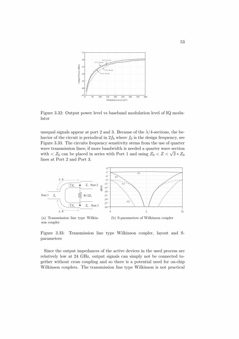
53
0 50 100 150 200 250 300 350 400-45
-40
-35
-30
-25
-20
-15
Modulation level (mV)
Outp
ut
Pow
er (
dB
m)
3.0 V, 107 mA
2.5 V, 85 mA
3.5 V, 129 mA
4.0 V, 151 mA
Figure 3.32: Output power level vs baseband modulation level of IQ modu-lator
unequal signals appear at port 2 and 3. Because of the λ/4-sections, the be-havior of the circuit is periodical in 2f0 where f0 is the design frequency, seeFigure 3.33. The circuits frequency sensitivity stems from the use of quarterwave transmission lines; if more bandwidth is needed a quarter wave sectionwith < Z0 can be placed in series with Port 1 and using Z0 < Z <
√2 ∗ Z0
lines at Port 2 and Port 3.
Port 1 Z0
2 Z0
2 Z0Z0
Z0
l 4
l 4
R=2Z0
Port 2
Port 3
(a) Transmission line type Wilkin-son coupler
f00 2f0
-27
-24
-21
-18
-15
-12
-9
-6
-3
-30
0
S22
S11
S32
S21
dB
(S)
(b) S-parameters of Wilkinson coupler
Figure 3.33: Transmission line type Wilkinson coupler, layout and S-parameters
Since the output impedances of the active devices in the used process arerelatively low at 24 GHz, output signals can simply not be connected to-gether without cross coupling and so there is a potential need for on-chipWilkinson couplers. The transmission line type Wilkinson is not practical
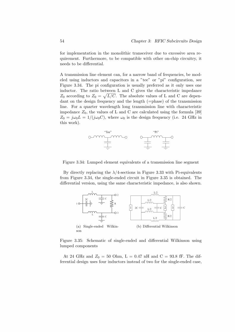
54 Chapter 3: RFIC Subcircuits Design
for implementation in the monolithic transceiver due to excessive area re-quirement. Furthermore, to be compatible with other on-chip circuitry, itneeds to be differential.
A transmission line element can, for a narrow band of frequencies, be mod-eled using inductors and capacitors in a ”tee” or ”pi” configuration, seeFigure 3.34. The pi configuration is usually preferred as it only uses oneinductor. The ratio between L and C gives the characteristic impedanceZ0 according to Z0 =
√
L/C. The absolute values of L and C are depen-dant on the design frequency and the length (=phase) of the transmissionline. For a quarter wavelength long transmission line with characteristicimpedance Z0, the values of L and C are calculated using the formula [39]Z0 = jω0L = 1/(jω0C), where ω0 is the design frequency (i.e. 24 GHz inthis work).
“Tee” “Pi”
Figure 3.34: Lumped element equivalents of a transmission line segment
By directly replacing the λ/4-sections in Figure 3.33 with Pi-equivalentsfrom Figure 3.34, the single-ended circuit in Figure 3.35 is obtained. Thedifferential version, using the same characteristic impedance, is also shown.
1
2
3
2C
L
L
C
C
R
(a) Single-ended Wilkin-son
L/2
L/2
L/2
L/2
1 2 32C
R/2
R/2
C C
(b) Differential Wilkinson
Figure 3.35: Schematic of single-ended and differential Wilkinson usinglumped components
At 24 GHz and Z0 = 50 Ohm, L = 0.47 nH and C = 93.8 fF. The dif-ferential design uses four inductors instead of two for the single-ended case,
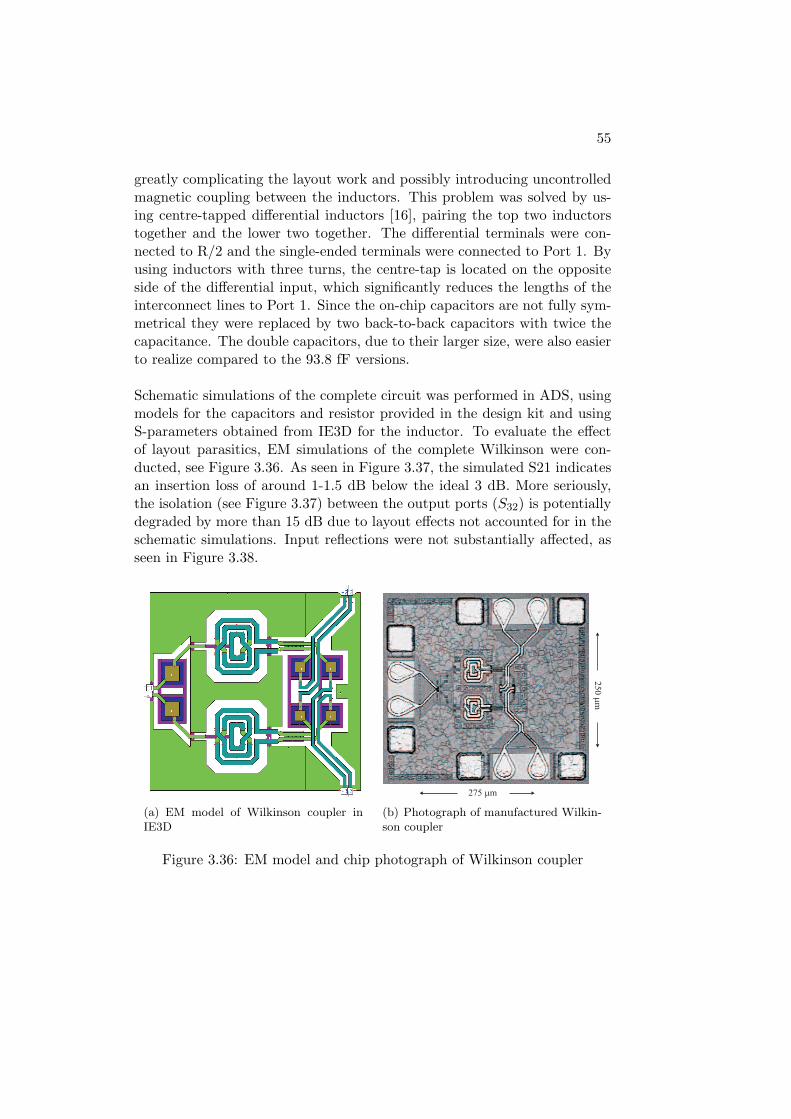
55
greatly complicating the layout work and possibly introducing uncontrolledmagnetic coupling between the inductors. This problem was solved by us-ing centre-tapped differential inductors [16], pairing the top two inductorstogether and the lower two together. The differential terminals were con-nected to R/2 and the single-ended terminals were connected to Port 1. Byusing inductors with three turns, the centre-tap is located on the oppositeside of the differential input, which significantly reduces the lengths of theinterconnect lines to Port 1. Since the on-chip capacitors are not fully sym-metrical they were replaced by two back-to-back capacitors with twice thecapacitance. The double capacitors, due to their larger size, were also easierto realize compared to the 93.8 fF versions.
Schematic simulations of the complete circuit was performed in ADS, usingmodels for the capacitors and resistor provided in the design kit and usingS-parameters obtained from IE3D for the inductor. To evaluate the effectof layout parasitics, EM simulations of the complete Wilkinson were con-ducted, see Figure 3.36. As seen in Figure 3.37, the simulated S21 indicatesan insertion loss of around 1-1.5 dB below the ideal 3 dB. More seriously,the isolation (see Figure 3.37) between the output ports (S32) is potentiallydegraded by more than 15 dB due to layout effects not accounted for in theschematic simulations. Input reflections were not substantially affected, asseen in Figure 3.38.
(a) EM model of Wilkinson coupler inIE3D
275 mm
25
0m
m
(b) Photograph of manufactured Wilkin-son coupler
Figure 3.36: EM model and chip photograph of Wilkinson coupler
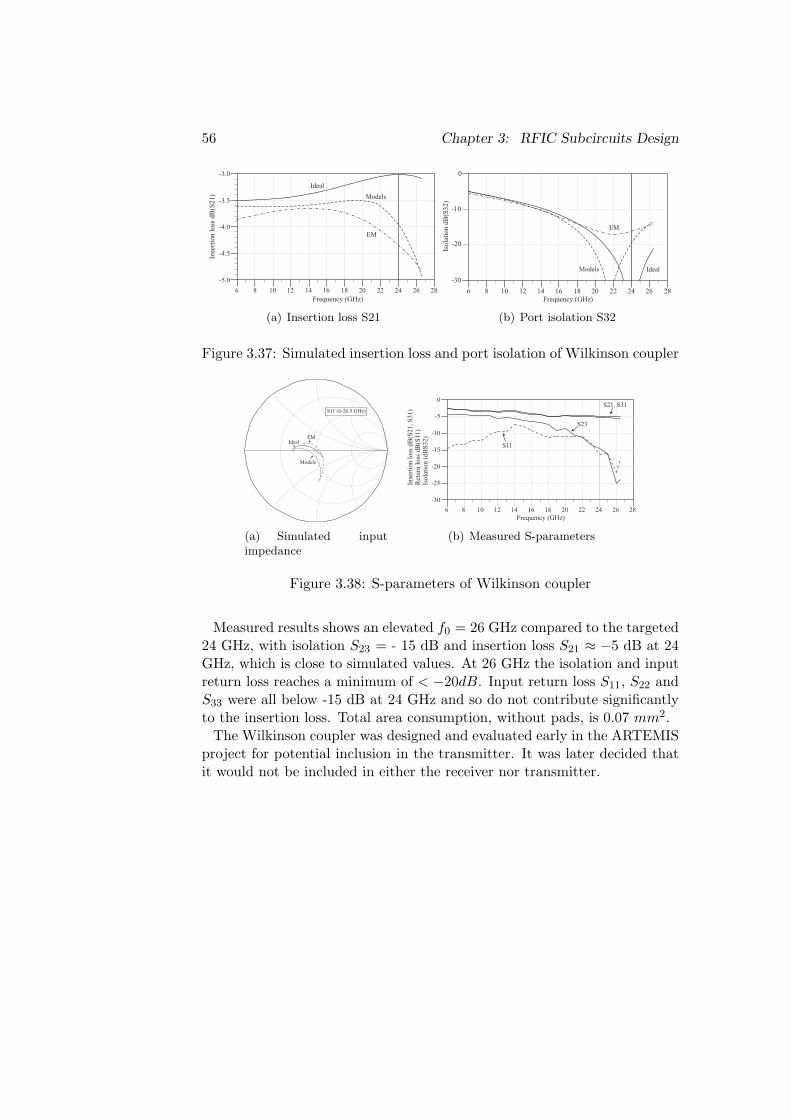
56 Chapter 3: RFIC Subcircuits Design
8 10 12 14 16 18 20 22 24 266 28
-4.5
-4.0
-3.5
-5.0
-3.0
Ideal
Models
EM
Inse
rtio
n l
oss
dB
(S2
1)
Frequency (GHz)
(a) Insertion loss S21
8 10 12 14 16 18 20 22 24 266 28
-10
-30
0
IdealModels
EM
Frequency (GHz)
-20
Iso
lati
on
dB
(S3
2)
(b) Port isolation S32
Figure 3.37: Simulated insertion loss and port isolation of Wilkinson coupler
IdealEM
Models
S11 (6-26.5 GHz)
(a) Simulated inputimpedance
8 10 12 14 16 18 20 22 24 266 28
-25
-20
-15
-10
-5
-30
0
Inse
rtio
n l
oss
dB
(S21, S
31)
Ret
urn
loss
dB
(S11)
Isola
tion (
dB
S32)
Frequency (GHz)
S21, S31
S11
S23
(b) Measured S-parameters
Figure 3.38: S-parameters of Wilkinson coupler
Measured results shows an elevated f0 = 26 GHz compared to the targeted24 GHz, with isolation S23 = - 15 dB and insertion loss S21 ≈ −5 dB at 24GHz, which is close to simulated values. At 26 GHz the isolation and inputreturn loss reaches a minimum of < −20dB. Input return loss S11, S22 andS33 were all below -15 dB at 24 GHz and so do not contribute significantlyto the insertion loss. Total area consumption, without pads, is 0.07 mm2.
The Wilkinson coupler was designed and evaluated early in the ARTEMISproject for potential inclusion in the transmitter. It was later decided thatit would not be included in either the receiver nor transmitter.
Chapter 4RFIC Systems
Using the components described in Chapter 3, complete receiver and trans-mitter systems have been designed and manufactured. Although all devicesfor the transmitter shows satisfactory results, the transmitter is not reportedin this thesis due to insufficient measured system performance (likely causedby DC biasing errors).
Two versions of the receiver has been included - with and without inte-grated VCO. For the version with integrated VCO, an LNA [6] designed byproject partner Ulm University, Germany, has been used. For the versionwithout integrated VCO, the LNA reported in this thesis was integrated.Furthermore, the 1/16 frequency divider (or prescaler) used was also devel-oped at Ulm University.
4.0.12 Monolithic Receiver with external LO
A fully differential 24 GHz receiver using an external LO source is shownin Figure 4.1, based on subcomponents reported in Chapter 3. A blockschematic of the system is shown in Figure 4.2. The Vcc terminal of eachcircuit block is connected through a local LC low pass filter before beingconnected together at the Vcc bond pad to minimize inter-circuit blocksignal coupling through the Vcc line. This type of coupling is further reduceddue to the complete differential topology throughout the system.
The receiver has a higher conversion gain and lower noise figure at 23 GHzinstead of the targeted 24 GHz, see Figure 4.3, which is directly related tothe higher LNA gain at 23 GHz. This is expected since the noise of the IQdemodulator (NF=20 dB) is not fully suppressed by the LNA. The inputcompression point was measured to -20 dBm, identical to that of the stand-
57
58 Chapter 4: RFIC Systems
Vcc
Vcc
+RF
-RF
+Q -Q
+I -I
+LO
-LO
LO amplifiers PF filter
1.5 mm
0.9
5 m
m
Vcc
Vcc
MixersLNA
Figure 4.1: Layout of receiver with external LO
alone LNA. This means that system performance can easily be increased byre-tuning the LNA frequency response for a 24 GHz gain peak without sacri-ficing receiver linearity. Further improvement can be achieved by connectingthe device by bond wires (or flip-chip technology) (as in a real application),choosing the wire lengths to add a series inductance to compensate for thecapacitive LNA input impedance. This would reduce the LNA noise figureand increase the gain, directly impacting system performance.
The receiver noise figure was measured by connecting the baseband outputvia a low frequency balun to a spectrum analyzer. As the system conversiongain is not sufficient to compensate for the spectrum analyzer noise floor, alow frequency amplifier was interposed in the signal chain. The noise figureof this amplifier was not removed from the presented receiver noise figure.
The conversion gain was measured by connecting the baseband output tothe 1 MΩ input port of a low frequency oscilloscope (through a balun).Phase and amplitude imbalance between the I and Q baseband channels,from phase and gain errors in the LO signals, was measured using the evalu-ation PCB (with a receiver having an integrated VCO) described in Section5.3, showing 22 and 0.1 dB imbalance respectively. Although the phaseimbalance is poor (typical acceptable values are 1 dB and 5 [11]), signal
59
00
00
1800
900
1800
2700
450
1350
2250
3150
Polyphase filter
II
IQ
QI
LO amplifiers
RF in
Mixers
Baseband I
Baseband Q
2 p
ole
s1 p
ole
LNA
LPF
LPF
LO in
Figure 4.2: Block schematic of receiver with external LO
processing techniques can be utilized to correct the I/Q constellations. Thelow amplitude error indicates that both mixers are working as intended inthe switching region; the phase error is most likely caused by the polyphasefilter not giving the correct 45 shift between the one and two pole sections.
Important measured characteristics are summarized in Table 4.1. Totalcurrent consumption was 170 mA at 3 V and total area consumption was1.4 mm2.
18 19 20 21 22 23 24 25 26 27-15
-10
-5
0
5
10
15
20
Co
nv
ersi
on
gai
n (
dB
)
Frequency (GHz)
(a) Conversion gain
20 21 22 23 24 25 266
8
10
12
14
16
18
20
22
Frequency (GHz)
No
ise
Fig
ure
(d
B)
(b) Noise figure
Figure 4.3: Measured conversion gain and noise figure of receiver with ex-ternal LO
60 Chapter 4: RFIC Systems
DC Power 170 mA @ 3 V
Conversion gain @ 1 MΩ 15 dB
P1dB,in -20 dBm
NFmin @ 100 Ω 7.5 dB
NF @ 100 Ω @ 24 GHz 9.0 dB
Table 4.1: Receiver with external LO measured characteristics
4.0.13 Monolithic Receiver with internal LO
A fully differential, fully monolithic receiver with integrated VCO is shownin Figure 4.4 with a block schematic in Figure 4.5. The LNA, developedat University of Ulm [6], is marked by a red box in the layout, with im-portant electrical characteristics compiled in Table 4.2. Other componentsare recognized from Chapter 3. All measurements have been conducted at asingle frequency (i.e. 24 GHz) due to the limited tuning range of the VCO.The Vcc terminal of each circuit block is connected through a local LC lowpass filter before being connected together at the Vcc bond pad to minimizeinter-circuit block signal coupling through the Vcc line
DC Power 55 mA @ 4 V
Gain @ 50Ω 21.5 dB
Isolation > 60 dB
P1dB,in -16.5 dBm
P1dB,out +4 dBm
NFmin 5.8 dB
Table 4.2: LNA characteristics
The system noise figure was 9 dB (at 24 GHz), which is identical to thenoise figure of the version with external LO signal (at 24 GHz) even thoughusing an LNA with higher gain and lower noise figure. This could be ex-plained by insufficient LO drive levels from the integrated VCO making alltransistors in the mixer switching quads contributing noise over the entireLO cycle. The good amplitude balance of the I and Q port however indi-cates that this is not the case. Another, more likely, explanation is thatthe LNA used with the external VCO was optimized for integration withthe I/Q mixers, thus providing higher gain on-chip than what was measuredusing 100 Ω load impedance.
A 35.5 dB conversion gain, with a 24 dB gain IF amplifier cascaded, wasmeasured by connecting the baseband output to a 1MOhm oscilloscope. By
61
2.14 mm
1.3
4 m
m
+RF
-RF
+Q -Q
LNA
Vcc
VCOctrl
Vcc VCO
Vcc Prescaler
+I -I
Prescaler out
Figure 4.4: Layout of receiver with internal LO
removing the 24 dB IF amplifier gain (ignoring eventual impedance miss-match effects) a total receiver conversion gain of 11.5 dB was obtained.The reduction of conversion gain compared to the receiver with external LOindicates that the mixers are operated in the multiplication region, which hasa lower gain and higher noise figure compared to when being fully switched.The linearity of the receiver is shown in Figure 4.6, with an input 1-dBcompression point of -25 dB (output power un-calibrated). This indicatesthat the mixers in the IQ-demodulator is the limiting device in the receiverin terms of linearity.
Total current consumption of the receiver was 240 mA at 3 V and totalarea consumption was 2.9 mm2. A version of the receiver using flip-chippads instead of wafer probe pads was also designed, as discussed in Section5.3.
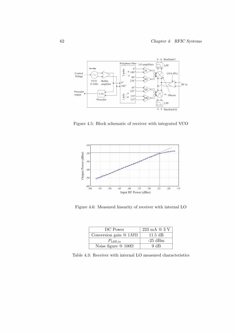
62 Chapter 4: RFIC Systems
00
00
1800
900
1800
2700
450
1350
2250
3150
Polyphase filter
II
IQ
QI
LO amplifiers
RF in
Mixers
Baseband I
Baseband Q
2 p
ole
s1
po
le
LNA (PA)
VCO
12 GHzBufferamplifier
1/16
On chip
LPF
LPF
ControlVoltage
Prescaleroutput
Prescaler
Figure 4.5: Block schematic of receiver with integrated VCO
-60 -55 -50 -45 -40 -35 -30 -25 -20 -15-60
-50
-40
-30
-20
-10
Input RF Power (dBm)
Outp
ut
Pow
er (
dB
m)
Figure 4.6: Measured linearity of receiver with internal LO
DC Power 223 mA @ 3 V
Conversion gain @ 1MΩ 11.5 dB
P1dB,in -25 dBm
Noise figure @ 100Ω 9 dB
Table 4.3: Receiver with internal LO measured characteristics
Chapter 5RFIC Packaging using LTCC
5.1 LTCC packaging concept
Multi-layer Low Temperature Co-fired Ceramic (LTCC) technology is apackaging solution that has attracted a lot of attention recently for RFapplications because of its exceptional high frequency electrical properties[40], including low substrate and metallic losses. Besides constituting anexcellent chip carrier due to low manufacturing tolerances (important be-cause of the dense pad placement in typical silicon devices), off-chip high-Qpassive components such as inductors, capacitors, transmission lines and an-tennas can be embedded in the module, reducing the total cost and size ofthe system. The particular LTCC material chosen for the ARTEMIS radardemonstrator was Ferro A6, see Table 5.1. For this application, since thereceiver and transmitter chips are fairly high power devices, the matchingthermal expansion coefficient of LTCC to silicon was an essential featurecompared to plastic packaging.
A four layer 10 x 7.5 mm2 module with a two layer deep cavity for theRFIC was designed to provide DC and baseband connections to the PCB, as
layer thickness 100 µm
min spacing 100 µm
εr 5.9
tan δ 0.002
metal 12 µm Ag
Table 5.1: Material and processing properties of Ferro A6 LTCC
63

64 Chapter 5: RFIC Packaging using LTCC
well as a 24 GHz high frequency transition from the differential on-chip in-put/output to the single ended PCB antenna. The cavity provides the chipmechanical protection and gives the on-LTCC transmission lines a homo-geneous dielectric environment fairly independent on whatever material (ifany) that is coating the LTCC module. Two different LTCC versions weremanufactured with different via designs for thermal management studies[41].
RFIC
L2
L1
Pads ViasConductors
Balun
Microstrip to striplinetransition
l/4
“Flaps” providing L1-L0ac connection
L0
RFIC
L0
L2
L1
RFIC
Pads Vias Conductors
Balun
Microstrip to striplinetransition
l/4
“Flaps” providing L1-L0ac connection
RFIC
L0
L2
L1
Figure 5.1: Layout of LTCC version 1 (left), with vias connecting all pads,and version 2 (right) with strips connecting all pads
The LTCC modules were mounted on the PCB using conventional solderpaste stencil printed on the joint areas. The RFICs were joined onto theLTCC module using flip chip technique. Gold stud bumps were made onthe chips using a wire bonder and the flip chip joining was made by thermocompression. Figure 5.1 shows the layout of the manufactured modules,mainly differing in the connections to the RFIC; all via connections (exceptfor the RF input) in the left figure and all strip connections in the right.
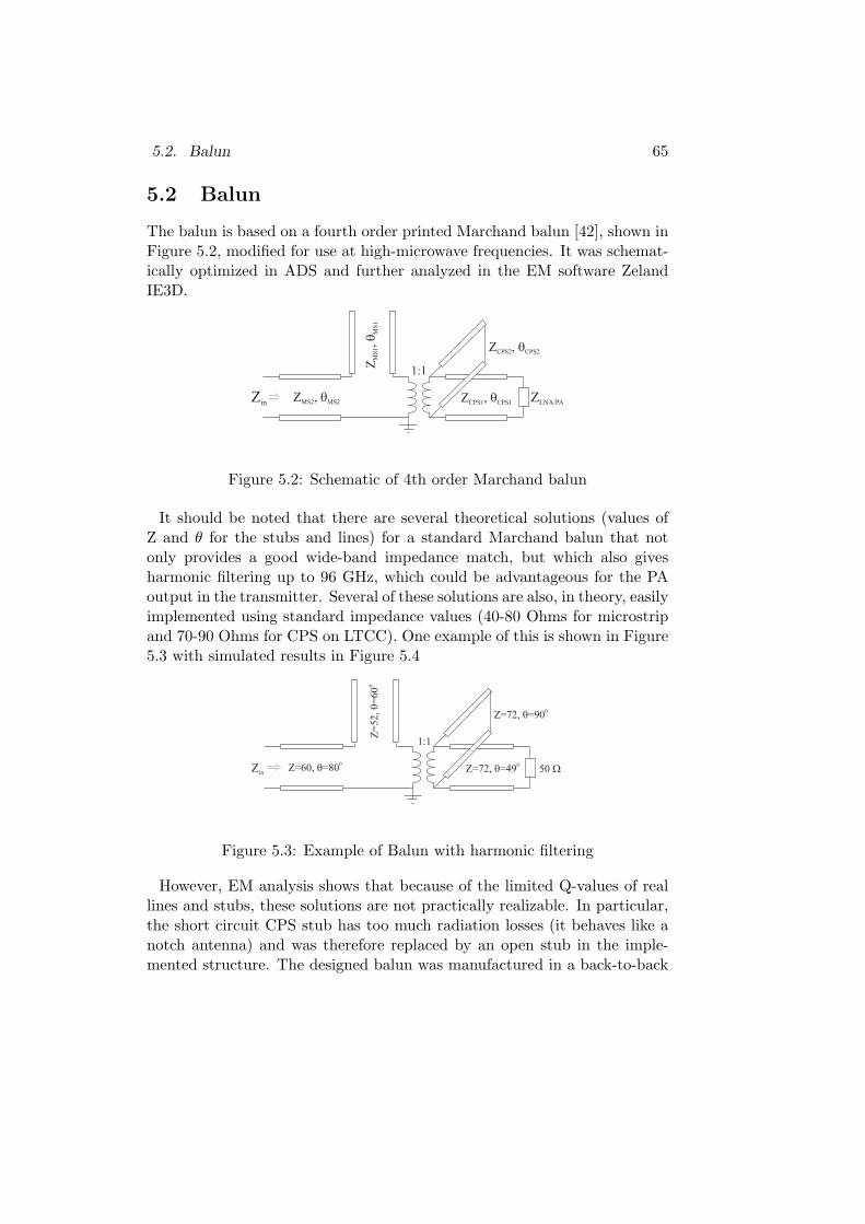
5.2. Balun 65
5.2 Balun
The balun is based on a fourth order printed Marchand balun [42], shown inFigure 5.2, modified for use at high-microwave frequencies. It was schemat-ically optimized in ADS and further analyzed in the EM software ZelandIE3D.
Z ,MS2 MS2q
Z,
MS
1M
S1
q
ZLNA/PAZin Z ,CPS1 CPS1q
1:1
Z ,CPS2 CPS2q
Figure 5.2: Schematic of 4th order Marchand balun
It should be noted that there are several theoretical solutions (values ofZ and θ for the stubs and lines) for a standard Marchand balun that notonly provides a good wide-band impedance match, but which also givesharmonic filtering up to 96 GHz, which could be advantageous for the PAoutput in the transmitter. Several of these solutions are also, in theory, easilyimplemented using standard impedance values (40-80 Ohms for microstripand 70-90 Ohms for CPS on LTCC). One example of this is shown in Figure5.3 with simulated results in Figure 5.4
50 WZin Z=72, =49q0
1:1
Z=72, =90q0
Z=
52
,=
60
q0
Z=60, =80q0
Figure 5.3: Example of Balun with harmonic filtering
However, EM analysis shows that because of the limited Q-values of reallines and stubs, these solutions are not practically realizable. In particular,the short circuit CPS stub has too much radiation losses (it behaves like anotch antenna) and was therefore replaced by an open stub in the imple-mented structure. The designed balun was manufactured in a back-to-back
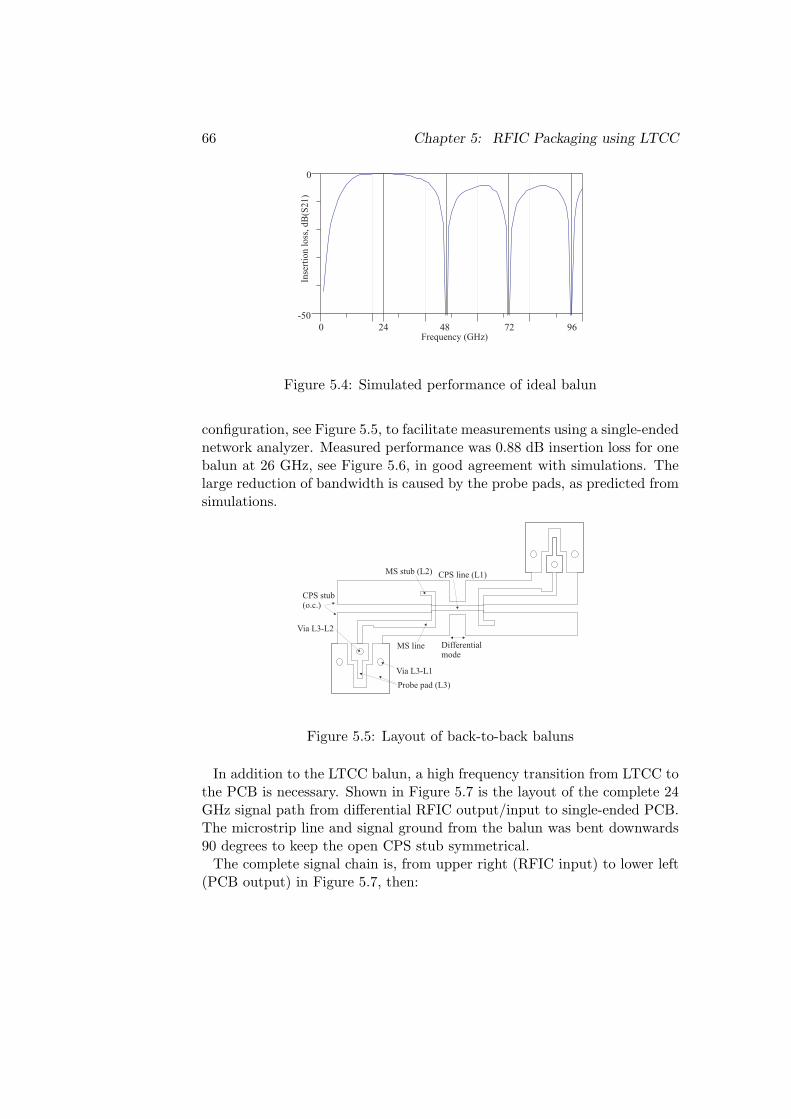
66 Chapter 5: RFIC Packaging using LTCC
720 96
-50
0
24 48Frequency (GHz)
Inse
rtio
n l
oss
, dB
(S21)
Figure 5.4: Simulated performance of ideal balun
configuration, see Figure 5.5, to facilitate measurements using a single-endednetwork analyzer. Measured performance was 0.88 dB insertion loss for onebalun at 26 GHz, see Figure 5.6, in good agreement with simulations. Thelarge reduction of bandwidth is caused by the probe pads, as predicted fromsimulations.
Differentialmode
MS stub (L2) CPS line (L1)
CPS stub(o.c.)
MS line
Via L3-L1
Via L3-L2
Probe pad (L3)
Figure 5.5: Layout of back-to-back baluns
In addition to the LTCC balun, a high frequency transition from LTCC tothe PCB is necessary. Shown in Figure 5.7 is the layout of the complete 24GHz signal path from differential RFIC output/input to single-ended PCB.The microstrip line and signal ground from the balun was bent downwards90 degrees to keep the open CPS stub symmetrical.
The complete signal chain is, from upper right (RFIC input) to lower left(PCB output) in Figure 5.7, then:
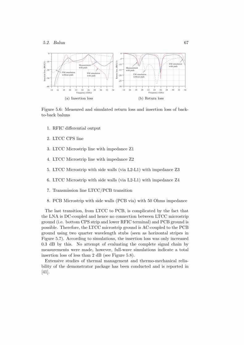
5.2. Balun 67
16 18 20 22 24 26 28 30 3214 34
-30
-20
-10
-40
0
Inse
rtio
n l
oss
, d
B(S
21
)
Frequency (GHz)
EM simulationwith pads
EM simulationwithout pads
Measurementwith pads
(a) Insertion loss
16 18 20 22 24 26 28 30 3214 34
-25
-20
-15
-10
-5
-30
0
Ret
urn
lo
ss,
dB
(S11
)
Frequency (GHz)
EM simulationwith pads
EM simulationwithout pads
Measurementwith pads
(b) Return loss
Figure 5.6: Measured and simulated return loss and insertion loss of back-to-back baluns
1. RFIC differential output
2. LTCC CPS line
3. LTCC Microstrip line with impedance Z1
4. LTCC Microstrip line with impedance Z2
5. LTCC Microstrip with side walls (via L2-L1) with impedance Z3
6. LTCC Microstrip with side walls (via L2-L1) with impedance Z4
7. Transmission line LTCC/PCB transition
8. PCB Microstrip with side walls (PCB via) with 50 Ohms impedance
The last transition, from LTCC to PCB, is complicated by the fact thatthe LNA is DC-coupled and hence no connection between LTCC microstripground (i.e. bottom CPS strip and lower RFIC terminal) and PCB ground ispossible. Therefore, the LTCC microstrip ground is AC-coupled to the PCBground using two quarter wavelength stubs (seen as horizontal stripes inFigure 5.7). According to simulations, the insertion loss was only increased0.3 dB by this. No attempt of evaluating the complete signal chain bymeasurements were made, however, full-wave simulations indicate a totalinsertion loss of less than 2 dB (see Figure 5.8).
Extensive studies of thermal management and thermo-mechanical relia-bility of the demonstrator package has been conducted and is reported in[41].
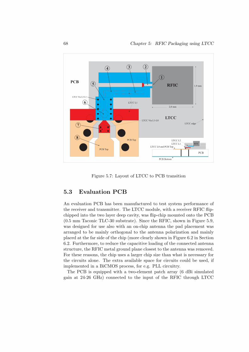
68 Chapter 5: RFIC Packaging using LTCC
LTCC
LTCC edge
1,9 mm
2,0 mm
LTCC Via L2-L1
LTCC L1
LTCC Via L1-L0
LTCC L2
LTCC L1
LTCC L0 and PCB Top
PCB
RFIC
PCB
PCB Top
PCB Top
RFIC
PCB Bottom
1
234
5
6
7
8
Figure 5.7: Layout of LTCC to PCB transition
5.3 Evaluation PCB
An evaluation PCB has been manufactured to test system performance ofthe receiver and transmitter. The LTCC module, with a receiver RFIC flip-chipped into the two layer deep cavity, was flip-chip mounted onto the PCB(0.5 mm Taconic TLC-30 substrate). Since the RFIC, shown in Figure 5.9,was designed for use also with an on-chip antenna the pad placement wasarranged to be mainly orthogonal to the antenna polarization and mainlyplaced at the far side of the chip (more clearly shown in Figure 6.2 in Section6.2. Furthermore, to reduce the capacitive loading of the connected antennastructure, the RFIC metal ground plane closest to the antenna was removed.For these reasons, the chip uses a larger chip size than what is necessary forthe circuits alone. The extra available space for circuits could be used, ifimplemented in a BiCMOS process, for e.g. PLL circuitry.
The PCB is equipped with a two-element patch array (6 dBi simulatedgain at 24-26 GHz) connected to the input of the RFIC through LTCC

5.3. Evaluation PCB 69
5 10 15 20 24 30 35 40 450 50
-15
-10
-5
-20
0
S21
S11
S22
S p
aram
eter
s (d
B)
Frequency (GHz)
Figure 5.8: Simulated insertion loss of RFIC to LTCC to PCB transition
transitions described in previous sections. All DC traces have one large (10uF) and one small capacitor (0.1 uF) to ground to shunt any noise pickedup by the PCB or cables. In addition, there are several on-chip capacitorbanks to shunt any 24 GHz signals coupled to the Vcc line.
The baseband signals are AC coupled to coaxial connectors through acenter-tapped transformer useable for 60 kHz to 400 MHz signals. Usingthe evaluation PCB, phase and amplitude balance of the IQ demodulatorcould be measured, as reported in Section 4. A full characterization of theevaluation PCB is still to be made.
2.0 mm
1.9
mm
Figure 5.9: Layout of receiver RFIC using flip-chip pads

70 Chapter 5: RFIC Packaging using LTCC
LTCC module
Patch antennaarray
Decouplingcapacitors
RFIC
Balun
Figure 5.10: Evaluation PCB with RFIC flip-chipped onto LTCC module
Chapter 6Conclusions and future work
6.1 Conclusions
This thesis has presented SiGe RFIC and LTCC packaging techniques demon-strating the feasibility of low-cost, compact short-range radar and commu-nication devices for the 24 GHz ISM band. Completely monolithic directconversion receiver and transmitter front-end chips have been manufacturedand evaluated. By using a fully differential topology and subharmonic mix-ers, the typical concerns off LO self mixing and second order distortionassociated with direct conversion have been addressed. While the receiverdisplays satisfactory performance for the targeted applications, the trans-mitter, although using verified subcomponents, showed insufficient systemperformance (probably due to biasing errors).
LTCC has been identified as a suitable chip carrier for millimeter-wavetransceiver packaging, targeting applications using off-chip high gain an-tennas. A 24 GHz low-loss chip-to-PCB transition has been designed andevaluated, including a Marchand balun that was modified for high frequencyoperation.
6.2 Future Work
One of the main objectives in the ARTEMIS project was the developmentof monolithic transceivers with on-chip antennas for use in Bluetooth-likeshort range communication devices. Since the antenna would be on-chip,no external high-frequency interconnects would be needed thus simplifyingpackaging requirements. For circuits on low-resistivity silicon, the antenna
71

72 Chapter 6: Conclusions and future work
metallization was deposited on a thin layer of BCB and the silicon was etchedaway in the vicinity of the antenna to remove substrate losses. For circuitson high-resistivity silicon, the top-most metal layer in the semiconductorprocess was used for the antenna metallization and no post-processing (likeetching) was deployed. Although this thesis has mainly focused on the radarapplication using a LTCC chip carrier, systems with integrated antennashave also been developed and manufactured. These systems, which so farhave not been characterized, are briefly described in the next two pagesof this section. Further suggestions on future work topics that could beinteresting include:
• Correcting the layout problems of the biasing circuitry in the trans-mitter with internal VCO (see Figure 6.1).
• Replacing all nitride capacitors with MIM capacitors
• Evaluating the true system performance of the transceivers in a radaror communication link application, with the integrated VCO locked toan external PLL.
• Thorough characterization of the evaluation PCB, especially the 24GHz RFIC-to-PCB transition.
• Replacing the LNA (re-tuned to 24 GHz) used in the receiver withintegrated VCO with the LNA optimized for the IQ demodulator.
2.14 mm
1.3
4 m
m
+RF
-RF
+Q -Q
Vcc
VCOctrl
Vcc VCO
Vcc Prescaler
+I -I
Prescaler out
Figure 6.1: Layout of transmitter with internal LO
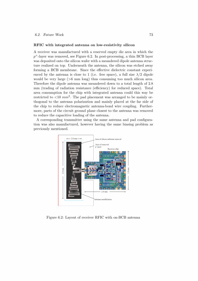
6.2. Future Work 73
RFIC with integrated antenna on low-resistivity silicon
A receiver was manufactured with a reserved empty die area in which thep+-layer was removed, see Figure 6.2. In post-processing, a thin BCB layerwas deposited onto the silicon wafer with a meandered dipole antenna struc-ture realized on top. Underneath the antenna, the silicon was etched awayforming a BCB membrane. Since the effective dielectric constant experi-enced by the antenna is close to 1 (i.e. free space), a full size λ/2 dipolewould be very large (>6 mm long) thus consuming too much silicon area.Therefore the dipole antenna was meandered down to a total length of 2.8mm (trading of radiation resistance (efficiency) for reduced space). Totalarea consumption for the chip with integrated antenna could this way berestricted to <10 mm2. The pad placement was arranged to be mainly or-thogonal to the antenna polarization and mainly placed at the far side ofthe chip to reduce electromagnetic antenna-bond wire coupling. Further-more, parts of the circuit ground plane closest to the antenna was removedto reduce the capacitive loading of the antenna.
A corresponding transmitter using the same antenna and pad configura-tion was also manufactured, however having the same biasing problem aspreviously mentioned.
2.0 mm
1.9
mm
Receiver chip
2.8
mm
2.8 mm
Area of removed
p layer+
Area of silicon substrate removal
Antenna metallization
Figure 6.2: Layout of receiver RFIC with on-BCB antenna
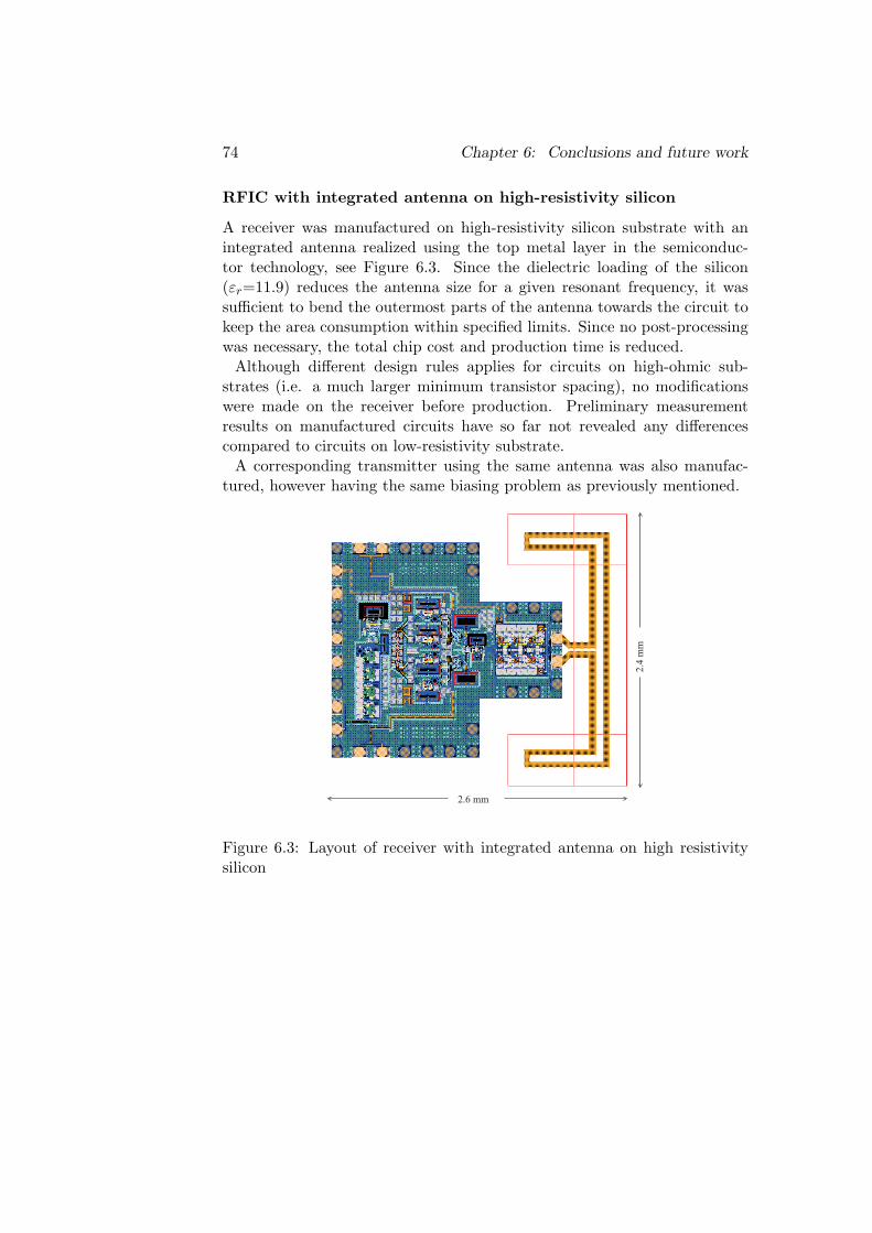
74 Chapter 6: Conclusions and future work
RFIC with integrated antenna on high-resistivity silicon
A receiver was manufactured on high-resistivity silicon substrate with anintegrated antenna realized using the top metal layer in the semiconduc-tor technology, see Figure 6.3. Since the dielectric loading of the silicon(εr=11.9) reduces the antenna size for a given resonant frequency, it wassufficient to bend the outermost parts of the antenna towards the circuit tokeep the area consumption within specified limits. Since no post-processingwas necessary, the total chip cost and production time is reduced.
Although different design rules applies for circuits on high-ohmic sub-strates (i.e. a much larger minimum transistor spacing), no modificationswere made on the receiver before production. Preliminary measurementresults on manufactured circuits have so far not revealed any differencescompared to circuits on low-resistivity substrate.
A corresponding transmitter using the same antenna was also manufac-tured, however having the same biasing problem as previously mentioned.
2.6 mm
2.4
mm
Figure 6.3: Layout of receiver with integrated antenna on high resistivitysilicon
Appendix AMeasurement Set-up
A.1 Wafer probing
All measurements have been conducted on-wafer using a probe station withGSSG (Ground-Signal-Signal-Ground) probes for signal inputs and outputsand needles for DC connections. The GSSG probes were connected to a6-26.5 GHz 1800 hybrid using two short, equal length, coaxial cables. Thehybrid converts the two 50 Ohm coaxial inputs, i.e. 100 Ohm differentialimpedance at the probe tips, into one 50 Ohm coaxial output that is con-nected to the measurement instrument. The probe station is placed inside ametal cage providing a common ground potential for all measurement equip-ment and wafer chuck to remove any potential ESD problems. The needleused for DC connection was connected to ground via the GSSG groundfingers using a wire.
-3 dB
-3 dB
D
S
GSSG
100
W
50 W
50 W
50 W
50 W
On-chip
Figure A.1: Coaxial 50Ω to GSSG probe tip 100Ω chain
S-parameters were measured using a 2 port Agilent E8364B PNA NetworkAnalyzer, calibrated using an on-wafer calibration kit (see Section A.1.1.
Noise figure measurements were conducted using an Agilent 8562A Spec-
75
76 Appendix A: Measurement Set-up
trum Analyzer. The RF port was fed by an Anritsu MH3694A SignalGenerator cascaded with a Pasternack 0-79 dB attenuator. The output(RF or baseband) was connected to low noise amplifiers with sufficient gainto suppress the noise figure of the Spectrum Analyzer and having a lowernoise figure than the gain of the device under test (thereby adding negli-gible noise). By measuring the output signal to noise ratio (S/N)out onthe Spectrum Analyzer and knowing (S/N)in (N=-174 dBm/Hz ensuredby the attenuator, S measured), the noise figure was calculated from thedefinition NF = (S/N)in/(S/N)out. For frequency conversion devices (i.e.mixers), only double side-band noise figures are reported. This value is 3 dBlower than the single side-band noise figure given by the spectrum analyzermeasurement.
Conversion gain for the down conversion mixers was measured by connect-ing the baseband output to a two channel low frequency oscilloscope with1 MOhm 20 pF input impedance. By inverting one channel and addingthe two signals, only the differential mode component was shown on thedisplay. Since conversion gain is traditionally taken as baseband (or IF)output power divided by input RF power, the output voltage was convertedto a power by assuming a 50 Ohm load impedance (which in practice canbe facilitated by using baseband buffer amplifers like emitter-followers). Ina real application, the baseband impedance is however most likely not 50Ohms.
It was not possible to measure both I and Q ports, or modulate bothports in the up-converter, on-wafer due to lack of available probes in themeasurement set-up. This means that phase and amplitude imbalance couldnot be measure on-wafer. These figures of merit were obtained for the LTCCpackaged receiver from measurements on the evaluation PCB described inSection 5.3.
Phase noise was measured using a Spectrum Analyzer.A typical measurement set-up for a receiver without integrated VCO is
shown in Figure A.2.
A.1.1 On wafer calibration kit
Most circuits measured are designed for use in an all on-chip environment,i.e. as an intrinsic part of the transceiver. The circuit is connected to bondpads (or probe pads) to facilitate on-chip measurements using probes, how-ever the pads are not integral to the circuit and its effect needs to be removedby de-embedding. For characterization of components such as inductors, it iscommon to use two de-embedding structures: a dummy short and a dummy
A.1. Wafer probing 77
-3 dB
-3 dB
D
S
GSSG
G S S G
-3 dB
-3 dB
D
S
00
00
1800
900
1800
2700
450
1350
2250
3150
Polyphasefilters
II
IQ
QI
LO pumpamplifiers
RF input
Sub-harmonicmixer cores
IF I
IF Q
Signal Generator24,2 GHz Oscillator
Spectrum Analyzer Oscilloscope
GSSG
SourceMeterDC
LNA
2 p
ole
s1
po
le
LO input
Figure A.2: Set-up for on-chip measurements of monolithic receiver
open [16]. After measurement of the device admittance YDUT , the dummyopen admittance Yopen and the dummy short impedance Zshort, the padsand pad-to-circuit interconnect lines can be effectively removed from themeasurement. This method requires some means of probe calibration, typ-ically using a commercial high quality calibration kit similar to standardcoaxial versions. Usually, this is done using single-ended GSG probes.
Through
Short
Open
2x50 loadW
G
S
S
G
Port
1
G
S
S
G
Port
2
Figure A.3: On-chip SOLT calibration kit
An alternative approach, used in this work, is to calibrate the networkanalyzer directly on-chip. To this end, a standard SOLT (short, open, load,through) kit was designed and manufactured as shown in Figure A.3. As is
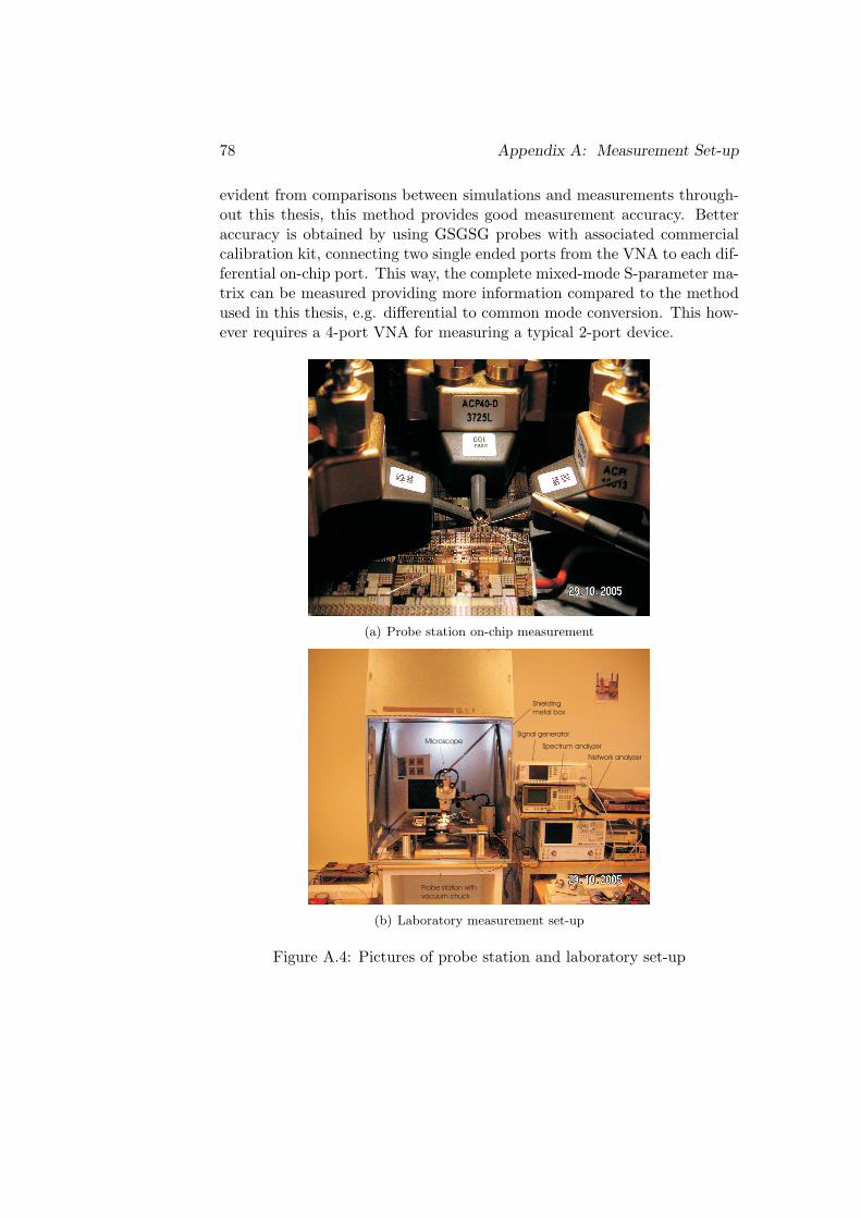
78 Appendix A: Measurement Set-up
evident from comparisons between simulations and measurements through-out this thesis, this method provides good measurement accuracy. Betteraccuracy is obtained by using GSGSG probes with associated commercialcalibration kit, connecting two single ended ports from the VNA to each dif-ferential on-chip port. This way, the complete mixed-mode S-parameter ma-trix can be measured providing more information compared to the methodused in this thesis, e.g. differential to common mode conversion. This how-ever requires a 4-port VNA for measuring a typical 2-port device.
(a) Probe station on-chip measurement
Shielding
metal box
Signal generator
Network analyzer
Probe station with
vacuum chuck
Spectrum analyzerMicroscope
(b) Laboratory measurement set-up
Figure A.4: Pictures of probe station and laboratory set-up
Bibliography
[1] E. Ojefors, F. Bouchriha, K. Grenier, and A. Rydberg, “24 GHz ISM-band antennas on surface micromachined substrates for integration witha commercial SiGe process,” ECWT Conference Proceedings, October2003.
[2] E. Ojefors and A. Rydberg, “LTCC and glob top packaging for 24 GHzMMIC with integrated antennas,” GigaHertz 03 Conference Proceed-ings, November 2003.
[3] ETSI, “En 302 288-1 v1.1.1 (2005-01),” 2005.
[4] H. H. Xiang Guan and A. Hajumiri, “A fully integrated 24-GHz eight-element phased-array receiver in silicon,” IEEE Journal of Solid-StateCircuits, vol. 39, pp. 2311–2320, December 2004.
[5] E. Sonmez, A. Trasser, K.-B. Schad, P. Abele, and H. Schumacher,“A single-chip 24 GHz receiver front-end using a commercially avail-able SiGe HBT foundry process,” in IEEE Radio Frequency IntegratedCircuits (RFIC) Symposium, (Seattle, WA), pp. 159–162, 2002.
[6] E. Soenmez, A. Trasser, P. Abele, K.-B. Schad, and H. Schumacher, “In-tegrated receiver components for low-cost 26 GHz LMDS applicationsusing an 0.8 µm SiGe HBT technology,” in 33rd European MicrowaveConference, (Munich), pp. 399–402, 2003.
[7] A. Ghazinour, P. Wennekers, J. Schmidt, Y. Yi, R. Reuter, and J. Tep-lik, “A fully-monolithic SiGe-BiCMOS transceiver chip for 24 GHz ap-plications,” IEEE Bipolar / BiCMOS Circuits and Technology Meeting,vol. 10, no. 1, pp. 181–184, 2003.
79
80 BIBLIOGRAPHY
[8] P. Wennekers, A. Ghazinour, and R. Reuter, “An integrated SiGe trans-mitter circuit for 24 GHz radar sensors,” IEEE Bipolar / BiCMOSCircuits and Technology Meeting, vol. 12, no. 2, pp. 212–215, 2002.
[9] V. Cannistraro, J.-C. Liou, and S. McCarter, “Direct modulation lowersVSAT equipment cost,” Microwaves and RF, pp. 99–101, August 1990.
[10] S. Kumar, “Directly modulated VSAT transmitter,” Microwave Jour-nal, pp. 255–264, April 1990.
[11] B. Razavi, RF Microelectronics. Prentice Hall, 1998.
[12] A. A. Abidi, “Direct-conversion radio transceivers for digital communi-cation,” IEEE Journal of Solid-State Circuits, vol. 30, pp. 1399–1410,December 1995.
[13] B. Razavi, “Design considerations for direct-conversion receivers,”IEEE Transactions on Circuits and Systems II: Analog and Digital Sig-nal Processing, vol. 44, pp. 428–435, June 1997.
[14] W. Namgoong and T. H. Meng, “Direct-conversion RF receiver design,”IEEE Transactions on Communications, vol. 49, pp. 518–529, March2001.
[15] A. Loke and F. Ali, “Direct conversion radio for digital mobile phones- design issues, status, and trends,” IEEE Transactions on MicrowaveTheory and Techniques.
[16] J. Rogers and C. Plett, Radio Frequency Integrated Circuit Design.Artech House, 2003.
[17] A. G. GmbH, “SIGE2RF.” Theresienstrasse 2, Heilbronn.
[18] B. J. et al, “Speed and power performance comparison of state-of-the-art CMOS and SiGe RF transistors,” in Topical Meeting on SiliconMonolithic Integrated Circuits in RF Systems Proceedings, pp. 115–118,September 2004.
[19] S. Sze, SEMICONDUCTOR DEVICES Physics and Technology. Wiley,second ed., 2002.
[20] J. D. Cressler and G. Niu, Silicon-Germanium Heterjunction BipolarTransistors. Artech House, first ed., 2003.
BIBLIOGRAPHY 81
[21] A. Schuppen, J. Berntgen, P. Maier, M. Tortschanoff, W. Krauss, andM. Averweg, “An 80 GHz SiGe production technology,” III-Vs Review,vol. 14, pp. 42–46, August 2001.
[22] D. Barlas, G. Henderson, X. Zhang, M. Bopp, and A. Schuppen, “SiGetransistor technology for RF applications,” Microwave Journal, June1999.
[23] J. E. James Angelo, Electronics: BJTs, FETs and Microcircuits.McGRAW-Hill, 1969.
[24] C. P. Yue and S. S. Wong, “On-chip spiral inductors with patternedground shields for Si-based RF IC’s,” IEEE Journal of Solid-State Cir-cuits, vol. 33, pp. 743–752, May 1998.
[25] J. H. Mikkelsen, O. K. Jensen, and T. Larsen, “Measurement and mod-eling of coupling effects of CMOS on-chip co-planar inductors,” in Top-ical Meeting on Silicon Monolithic Integrated Circuits in RF SystemsProceedings, pp. 37–40, September 2004.
[26] G. Ponchak, A. Margomenos, and L. Katehi, “Low-loss CPW on low-resistivity Si substrates with a micromachined polyimide interface layerfor RFIC interconnects,” IEEE Transactions on Microwave Theory andTechniques, vol. 49, pp. 866–870, May 2001.
[27] G. Ponchak, A. Margomenos, and P. Katehi, “Low loss finite widthground plane, thin film microstrip lines on Si wafers,” in Topical Meet-ing on Silicon Monolithic Integrated Circuits in RF Systems Proceed-ings, pp. 43–47, April 2000.
[28] H. Berg, H. Jacobsson, T. Lewin, K. Berg, A. Schuppen, and S. Gevor-gian, “Low loss passive microwave components in standard silicon tech-nology,” MTT-S, vol. 2, pp. 1153–1156, 2000.
[29] P. Horowitz and W. Hill, The Art of Electronics. Cambridge UniversityPress, second ed., 1989.
[30] D. B. Leeson, “A simple model of feedback oscillator noise spectrum,”Proc. IEEE, vol. 54, pp. 329–330, February 1966.
[31] T. H. L. abd Ali Hajimiri, “Oscillator phase noise: A tutorial,” IEEEJournal of Solid-State Circuits, vol. 35, pp. 326–336, March 2000.
82 BIBLIOGRAPHY
[32] B. Gilbert, “The multi-tanh principle: A tutorial overview,” IEEEJournal of Solid-State Circuits, vol. 33, pp. 2–17, Januray 1998.
[33] J. J. L. Sheng and L. Larsen, “A wide-bandwidth Si/SiGe HBT di-rect conversion sub-harmonic mixer/downconverter,” IEEE Journal ofSolid-State Circuits, vol. 35, pp. 1329–1336, September 2000.
[34] J. Chroma, “A three-level broad-banded monolithic analog multiplier,”IEEE Journal of Solid-State Circuits, vol. SC-16, pp. 392–399, August1981.
[35] S. Voinigescu, M. Maliepaard, J. Showell, G. Babcock, D. Marchesan,M. Schroter, P. Schvan, and D. Harame, “A scalable high-frequencynoise model for bipolar transistors with applications to optimal transis-tor sizing for low-noise amplifier design,” IEEE Journal of Solid-StateCircuits, vol. 32, pp. 1430–1439, September 1997.
[36] S. Chartier, E. Sonmez, and H. Schumacher, “24 and 36 GHz SiGe HBTpower amplifiers,” in Topical Meeting on Silicon Monolithic IntegratedCircuits in RF Systems Proceedings, pp. 251–254, September 2004.
[37] E. Wilkinson, “An n-way hybrid power divider,” IRE Transactions onMicrowave Theory and Techniques, vol. 8, pp. 116–118, January 1960.
[38] D. M. Pozar, Microwave Engineering. Wiley, second ed., 1998.
[39] J. E. Penn, “Convert distributed MICs to MMICs,” in Microwaves andRF, pp. 62–68, July 2003.
[40] K. Wu and Y. Huang, “LTCC technology and its applications in highfrequency front end modules,” Conf. Proceedings of 6th Internationalsymposium on Antennas, Propagation and EM Theory, pp. 730–734,October 2003.
[41] J. Lenkkeri, E. Juntunen, P. Lindberg, E. Ojefors, and A. Rydberg,“Packaging issues of 24 GHz traffic control radar front end based onSiGe and LTCC technologies,” IMAPS Nordic Conference Proceedings,September 2005.
[42] V. Trifunovic and B. Jokanovic, “Review of printed marchand anddouble y baluns: Characteristics and application,” IEEE Transactionson Microwave Theory and Techniques, vol. 42, pp. 1454–1462, August1994.