Embed Size (px)
Citation preview
101 Innovation DriveSan Jose, CA 95134www.altera.com
UG-01009-3.0
User Guide
RAM-Based Shift Register (ALTSHIFT_TAPS) IP Core
Document last updated for Altera Complete Design Suite version:Document publication date:
14.0June 2014
Subscribe
RAM-Based Shift Register (ALTSHIFT_TAPS) IP Core User Guide

RAM-Based Shift Register (ALTSHIFT_TAPS) IP Core User Guide June 2014 Altera Corporation
© 2014 Altera Corporation. All rights reserved. ALTERA, ARRIA, CYCLONE, HARDCOPY, MAX, MEGACORE, NIOS, QUARTUS and STRATIX are Reg. U.S. Pat.& Tm. Off. and/or trademarks of Altera Corporation in the U.S. and other countries. All other trademarks and service marks are the property of their respectiveholders as described at www.altera.com/common/legal.html. Altera warrants performance of its semiconductor products to current specifications in accordancewith Altera’s standard warranty, but reserves the right to make changes to any products and services at any time without notice. Altera assumes no responsibility orliability arising out of the application or use of any information, product, or service described herein except as expressly agreed to in writing by Altera. Alteracustomers are advised to obtain the latest version of device specifications before relying on any published information and before placing orders for products orservices.
June 2014 Altera Corporation
1. About this IP Core
This document describes the Altera-provided a RAM-based shift register (ALTSHIFT_TAPS) megafunction IP core. This IP core contains features not found in a conventional shift register. Traditional shift registers implemented with standard flip-flops use many logic cells for large shift registers. The ALTSHIFT_TAPS IP core is implemented in the device memory blocks, saving logic cells and routing resources. In a complicated design such as a digital signal processing (DSP) application that requires local data storage, it is more efficient to implement an ALTSHIFT_TAPS IP core as the shift register.
The ALTSHIFT_TAPS IP core is a parameterized shift register with taps. The taps provide data outputs from the shift register at certain points in the shift register chain. You can add additional logic that uses the output from these taps for further applications. The IP core’s output tap feature is useful for applications such as the Linear Feedback Shift Register (LFSR) and Finite Impulse Response (FIR) filters.
FeaturesThe ALTSHIFT_TAPS IP core implements a shift register with taps and offers additional features, which include:
■ Selectable RAM block type
■ A wide range of widths for the shiftin and shiftout ports
■ Support for output taps at certain points in the shift register chain
■ Selectable distance between taps
General DescriptionUse the IP Catalog (Tools > IP Catalog) and parameter editor to easily configure the IP core. The ALTSHIFT_TAPS IP core is implemented in the embedded memory block of all supported device families with simple dual-port RAM. You can select the RAM block type according to the capacity you require. The capacity that is represented by the width and the depth of the memory block depends on the TAP_DISTANCE, NUMBER_OF_TAPS, and WIDTH parameters of the ALTSHIFT_TAPS IP core.
f For the features and capacities of the typical memory block, refer to the chapter of your device handbook that contains information about TriMatrix embedded memory blocks.
The ALTSHIFT_TAPS IP core supports single-bit and multiple-bit data shifting at one clock cycle, depending on the width of the shiftin and shiftout ports. For example, if the shiftin and shiftout ports are single-bit data, only one bit is shifted per clock cycle. If the shiftin and shiftout ports are multiple-bit data, such as one-word data (8-bit), the whole word is shifted per clock cycle.
RAM-Based Shift Register (ALTSHIFT_TAPS) IP Core User Guide
1–2 Chapter 1: About this IP CoreGeneral Description
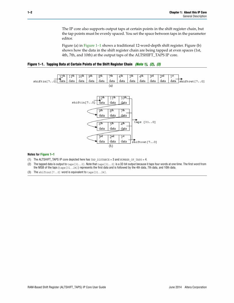
The IP core also supports output taps at certain points in the shift register chain, but the tap points must be evenly spaced. You set the space between taps in the parameter editor.
Figure (a) in Figure 1–1 shows a traditional 12-word-depth shift register. Figure (b) shows how the data in the shift register chain are being tapped at even spaces (1st, 4th, 7th, and 10th) at the output taps of the ALTSHIFT_TAPS IP core.
Figure 1–1. Tapping Data at Certain Points of the Shift Register Chain (Note 1), (2), (3)
Notes for Figure 1–1
(1) The ALTSHIFT_TAPS IP core depicted here has TAP_DISTANCE = 3 and NUMBER_OF_TAPS = 4.(2) The tapped data is output to taps[31..0]. Note that taps[31..0] is a 32-bit output because it taps four words at one time. The first word from
the MSB of the taps (taps[31..24]) represents the first data and is followed by the 4th data, 7th data, and 10th data.(3) The shiftout[7..0] word is equivalent to taps[31..24].
RAM-Based Shift Register (ALTSHIFT_TAPS) IP Core User Guide June 2014 Altera Corporation
June 2014 Altera Corporation
2. Using Altera IP Cores
Installing and Licensing IP CoresThe Quartus II software includes the Altera IP Library. The library provides many useful IP core functions for production use without additional license. You can fully evaluate any licensed Altera IP core in simulation and in hardware until you are satisfied with its functionality and performance.
Some Altera IP cores, such as MegaCore® functions, require that you purchase a separate license for production use. After you purchase a license, visit the Self Service Licensing Center to obtain a license number for any Altera product. For additional information, refer to Altera Software Installation and Licensing.
1 The default installation directory on Windows is <drive>:\altera\<version number>; on Linux it is <home directory>/altera/<version number>.
IP Catalog and Parameter EditorThe Quartus II IP Catalog (Tools > IP Catalog) and parameter editor help you easily customize and integrate IP cores into your project. You can use the IP Catalog and parameter editor to select, customize, and generate files representing your custom IP variation.
The IP Catalog automatically displays the IP cores available for your target device. Double-click any IP core name to launch the parameter editor and generate files representing your IP variation. The parameter editor prompts you to specify your IP variation name, optional ports, architecture features, and output file generation options. The parameter editor generates a top-level .qsys or .qip file representing the IP core in your project. Alternatively, you can define an IP variation without an open Quartus II project. When no project is open, select the Device Family directly in IP Catalog to filter IP cores by device.
1 The IP Catalog is also available in Qsys (View > IP Catalog). The Qsys IP Catalog includes exclusive system interconnect, video and image processing, and other system-level IP that are not available in the Quartus II IP Catalog.
Use the following features to help you quickly locate and select an IP core:
■ Filter IP Catalog to Show IP for active device family or Show IP for all device families.
Figure 2–1. IP core Installation Path
acds
quartus - Contains the Quartus II software
ip - Contains the Altera IP Library and third-party IP cores
altera - Contains the Altera IP Library source code
<IP core name> - Contains the IP core source files
RAM-Based Shift Register (ALTSHIFT_TAPS) IP Core User Guide
2–2 Chapter 2: Using Altera IP CoresUsing the Parameter Editor
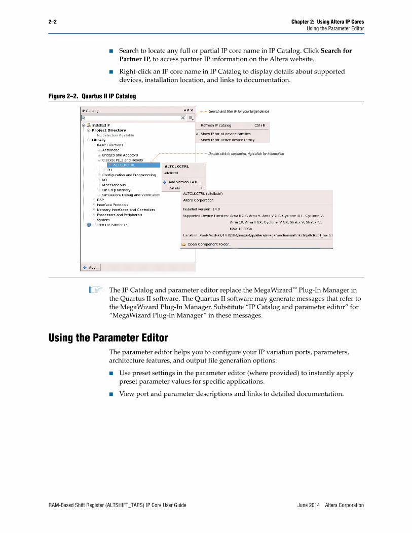
■ Search to locate any full or partial IP core name in IP Catalog. Click Search for Partner IP, to access partner IP information on the Altera website.
■ Right-click an IP core name in IP Catalog to display details about supported devices, installation location, and links to documentation.
1 The IP Catalog and parameter editor replace the MegaWizard™ Plug-In Manager in the Quartus II software. The Quartus II software may generate messages that refer to the MegaWizard Plug-In Manager. Substitute “IP Catalog and parameter editor” for “MegaWizard Plug-In Manager” in these messages.
Using the Parameter EditorThe parameter editor helps you to configure your IP variation ports, parameters, architecture features, and output file generation options:
■ Use preset settings in the parameter editor (where provided) to instantly apply preset parameter values for specific applications.
■ View port and parameter descriptions and links to detailed documentation.
Figure 2–2. Quartus II IP Catalog
Search and filter IP for your target device
Double-click to customize, right-click for information
RAM-Based Shift Register (ALTSHIFT_TAPS) IP Core User Guide June 2014 Altera Corporation
Chapter 2: Using Altera IP Cores 2–3Customizing and Generating IP Cores
■ Generate testbench systems or example designs (where provided).
Customizing and Generating IP CoresYou can customize IP cores to support a wide variety of applications. The Quartus II IP Catalog displays IP cores available for the current target device. The parameter editor guides you to set parameter values for optional ports, features, and output files.
To customize and generate a custom IP core variation, follow these steps:
1. In the IP Catalog (Tools > IP Catalog), locate and double-click the name of the IP core to customize. The parameter editor appears.
2. Specify a top-level name for your custom IP variation. This name identifies the IP core variation files in your project. If prompted, also specify the target Altera device family and output file HDL preference. Click OK.
3. Specify the desired parameters, output, and options for your IP core variation:
■ Optionally select preset parameter values. Presets specify all initial parameter values for specific applications (where provided).
■ Specify parameters defining the IP core functionality, port configuration, and device-specific features.
■ Specify options for generation of a timing netlist, simulation model, testbench, or example design (where applicable).
■ Specify options for processing the IP core files in other EDA tools.
4. Click Finish or Generate to generate synthesis and other optional files matching your IP variation specifications. The parameter editor generates the top-level .qip or .qsys IP variation file and HDL files for synthesis and simulation. Some IP cores also simultaneously generate a testbench or example design for hardware testing.
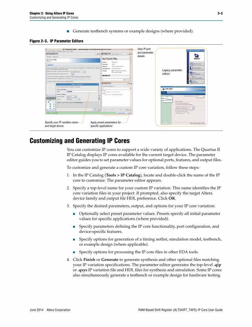
Figure 2–3. IP Parameter Editors
View IP portand parameter details
Apply preset parameters forspecific applications
Specify your IP variation nameand target device
Legacy parameter editors
June 2014 Altera Corporation RAM-Based Shift Register (ALTSHIFT_TAPS) IP Core User Guide
2–4 Chapter 2: Using Altera IP CoresUpgrading Outdated IP Cores
When you generate the IP variation with a Quartus II project open, the parameter editor automatically adds the IP variation to the project. Alternatively, click Project > Add/Remove Files in Project to manually add a top-level .qip or .qsys IP variation file to a Quartus II project. To fully integrate the IP into the design, make appropriate pin assignments to connect ports. You can define a virtual pin to avoid making specific pin assignments to top-level signals.
Upgrading Outdated IP CoresEach IP core has a release version number that corresponds to its Quartus II software release. When you include IP cores from a previous version of the Quartus II software in your project, click Project > Upgrade IP Components to identify and upgrade any outdated IP cores.
The Quartus II software prompts you to upgrade an IP core when the latest version includes port, parameter, or feature changes. The Quartus II software also notifies you when IP cores are unsupported or cannot upgrade in the current version of the Quartus II software. Most Altera IP cores support automatic simultaneous upgrade, as indicated in the Upgrade IP Components dialog box. IP cores unsupported by auto-upgrade may require regeneration in the parameter editor, as indicated in the Upgrade IP Components dialog box.
Upgrading IP cores changes your original design files. If you have not already preserved your original source files, click Project > Archive Project and save the project archive.
To upgrade outdated IP cores, follow these steps:
1. In the latest version of the Quartus II software, open the Quartus II project containing an outdated IP core variation.
1 File paths in a restored project archive must be relative to the project directory and you must reference the IP variation .v or .vhd file or .qsys file, not the .qip file.
2. Click Project > Upgrade IP Components. The Upgrade IP Components dialog box displays all outdated IP cores in your project, along with basic instructions for upgrading each core.
3. To simultaneously upgrade all IP cores that support automatic upgrade, click Perform Automatic Upgrade. The IP variation upgrades to the latest version.
4. To upgrade IP cores unsupported by automatic upgrade, follow these steps:
a. Select the IP core in the Upgrade IP Components dialog box.
b. Click Upgrade in Editor. The original parameter editor appears.
c. Click Finish or Generate to regenerate the IP variation and complete the upgrade. The version number updates when complete.
RAM-Based Shift Register (ALTSHIFT_TAPS) IP Core User Guide June 2014 Altera Corporation
Chapter 2: Using Altera IP Cores 2–5
1 Example designs provided with any Altera IP core regenerate automatically whenever you upgrade the IP core in the Upgrade IP Components dialog box.
Upgrading IP Cores at the Command LineAlternatively, you can upgrade IP cores at the command line. To upgrade a single IP core, type the following command:
quartus_sh --ip_upgrade -variation_files <my_ip_path> <project>
To upgrade a list of IP cores, type the following command:
quartus_sh --ip_upgrade -variation_files"<my_ip>.qsys;<my_ip>.<hdl>; <project>"
1 IP cores older than Quartus II software version 12.0 do not support upgrade. Altera verifies that the current version of the Quartus II software compiles the previous version of each IP core. The MegaCore IP Library Release Notes reports any verification exceptions for MegaCore IP. The Quartus II Software and Device Support Release Notes reports any verification exceptions for other IP cores. Altera does not verify compilation for IP cores older than the previous two releases.
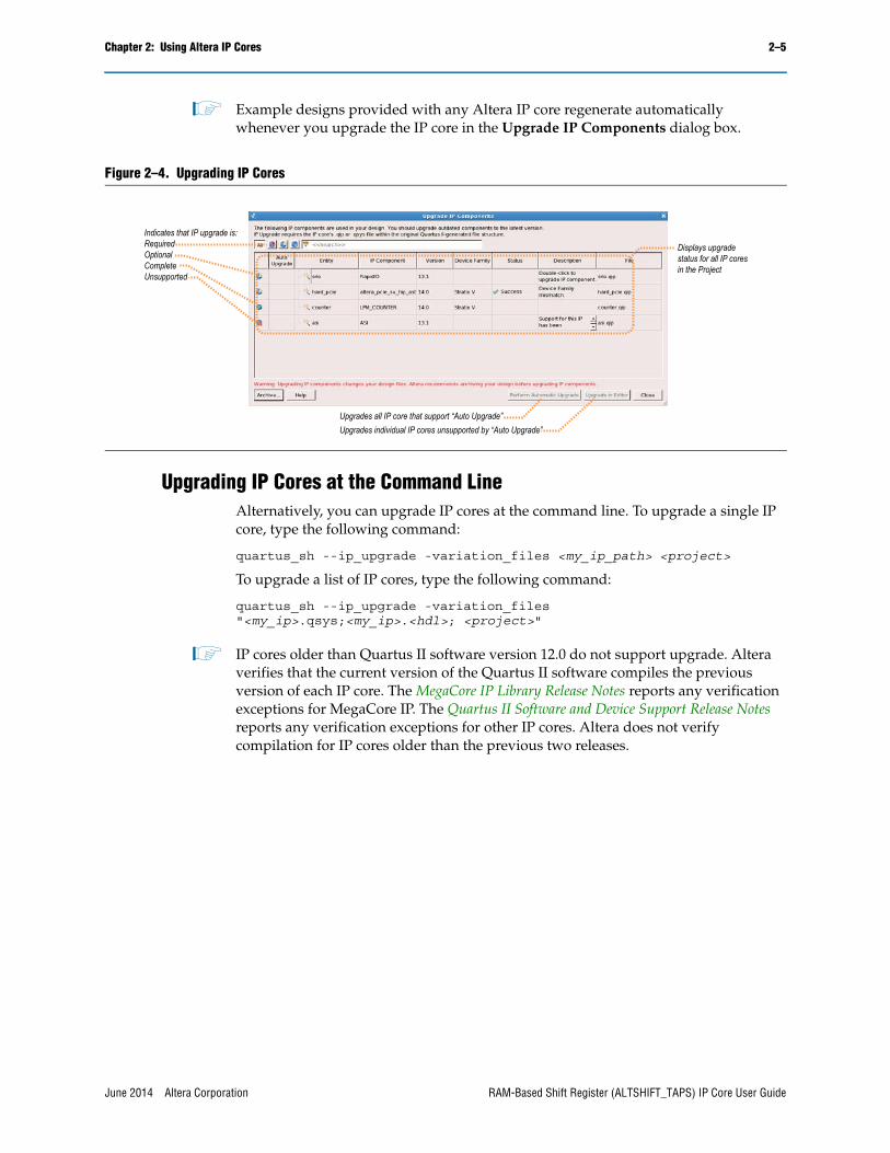
Figure 2–4. Upgrading IP Cores
Displays upgradestatus for all IP coresin the Project
Upgrades all IP core that support “Auto Upgrade”Upgrades individual IP cores unsupported by “Auto Upgrade”
Indicates that IP upgrade is:RequiredOptionalCompleteUnsupported
June 2014 Altera Corporation RAM-Based Shift Register (ALTSHIFT_TAPS) IP Core User Guide

2–6 Chapter 2: Using Altera IP Cores
RAM-Based Shift Register (ALTSHIFT_TAPS) IP Core User Guide June 2014 Altera Corporation
June 2014 Altera Corporation
3. Parameter Settings
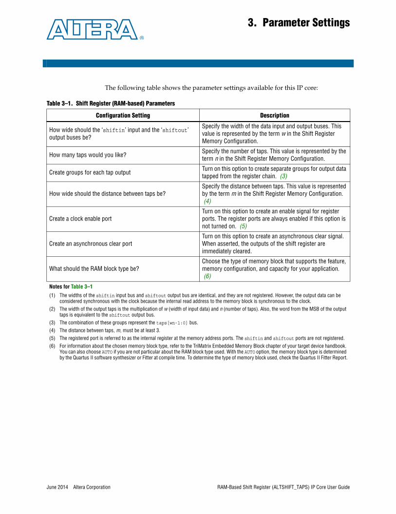
The following table shows the parameter settings available for this IP core:
Table 3–1. Shift Register (RAM-based) Parameters
Configuration Setting Description
How wide should the ‘shiftin’ input and the ‘shiftout’ output buses be?
Specify the width of the data input and output buses. This value is represented by the term w in the Shift Register Memory Configuration.
How many taps would you like? Specify the number of taps. This value is represented by the term n in the Shift Register Memory Configuration.
Create groups for each tap output Turn on this option to create separate groups for output data tapped from the register chain. (3)
How wide should the distance between taps be?Specify the distance between taps. This value is represented by the term m in the Shift Register Memory Configuration. (4)
Create a clock enable portTurn on this option to create an enable signal for register ports. The register ports are always enabled if this option is not turned on. (5)
Create an asynchronous clear portTurn on this option to create an asynchronous clear signal. When asserted, the outputs of the shift register are immediately cleared.
What should the RAM block type be?Choose the type of memory block that supports the feature, memory configuration, and capacity for your application. (6)
Notes for Table 3–1
(1) The widths of the shiftin input bus and shiftout output bus are identical, and they are not registered. However, the output data can be considered synchronous with the clock because the internal read address to the memory block is synchronous to the clock.
(2) The width of the output taps is the multiplication of w (width of input data) and n (number of taps). Also, the word from the MSB of the output taps is equivalent to the shiftout output bus.
(3) The combination of these groups represent the taps[wn-1:0] bus.(4) The distance between taps, m, must be at least 3.(5) The registered port is referred to as the internal register at the memory address ports. The shiftin and shiftout ports are not registered.(6) For information about the chosen memory block type, refer to the TriMatrix Embedded Memory Block chapter of your target device handbook.
You can also choose AUTO if you are not particular about the RAM block type used. With the AUTO option, the memory block type is determined by the Quartus II software synthesizer or Fitter at compile time. To determine the type of memory block used, check the Quartus II Fitter Report.
RAM-Based Shift Register (ALTSHIFT_TAPS) IP Core User Guide

3–2 Chapter 3: Parameter Settings
RAM-Based Shift Register (ALTSHIFT_TAPS) IP Core User Guide June 2014 Altera Corporation
June 2014 Altera Corporation
4. Specifications
This chapter describes the prototypes, declarations, ports, and parameters of the ALTSHIFT_TAPS IP core. You can use the ports and parameters to customize the ALTSHIFT_TAPS IP core according to your application.
Verilog HDL Prototype for the ALTSHIFT_TAPSYou can locate the following Verilog HDL prototype in the Verilog Design File (.v) altera_mf.v in the <Quartus II installation directory>\eda\synthesis directory.
module altshift_taps#( parameter intended_device_family = “unused”,
parameter number of taps = 1,parameter power_up_state = “CLEARED”,parameter taps_distance = 1,parameter width = 1,parameter lpm_type = “altshift_taps”,parameter lpm_hint = “unused”)
( input wire aclr,input wire clken,input wire clock,input wire [width-1:0] shiftin,output wire [width-1:0] shiftout,output wire [width*number_of_taps-1:0] taps)/*synthesis syn_black_box=1 */;
endmodule \\altshift_taps
VHDL Component Declaration for the ALTSHIFT_TAPSYou can locate the following VHDL Design File (.vhd) altera_mf.vhd in the <Quartus II installation directory>\libraries\bhdl\altera_mf directory.
component altshift_tapsgeneric (
intended_device_family : string := “unused”;number_of_taps : natural;power_up_state : string := “CLEARED”;tap_distance : natural;width : natural;lpm_hint : string := “UNUSED”;lpm_type : string := “altshift_taps”
);port(
aclr : in std_logic := ‘0’;clken : in std_logic := ‘1’;clock : in std_logic;shiftin: in std_logic_vector(width-1 downto 0);shiftout : out std_logic_vector(width-1 downto 0);taps : out std_logic_vector(width*number_of_taps-1 downto 0)
);end component;
RAM-Based Shift Register (ALTSHIFT_TAPS) IP Core User Guide
4–2 Chapter 4: SpecificationsVHDL Library-Use Declaration
VHDL Library-Use DeclarationThe VHDL LIBRARY-USE declaration is not required if you use the VHDL component declaration.
LIBRARY alterea_mf;USE altera_mf.altera_mf_components.all;
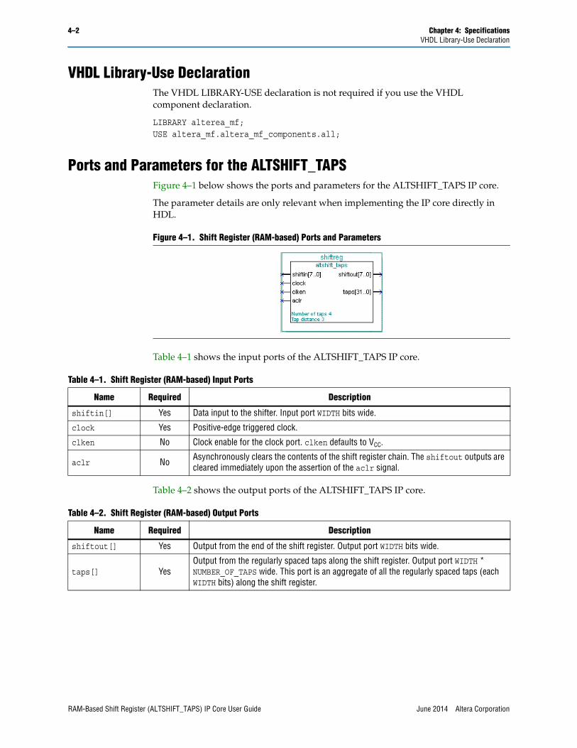
Ports and Parameters for the ALTSHIFT_TAPSFigure 4–1 below shows the ports and parameters for the ALTSHIFT_TAPS IP core.
The parameter details are only relevant when implementing the IP core directly in HDL.
Table 4–1 shows the input ports of the ALTSHIFT_TAPS IP core.
Table 4–2 shows the output ports of the ALTSHIFT_TAPS IP core.
Figure 4–1. Shift Register (RAM-based) Ports and Parameters
Table 4–1. Shift Register (RAM-based) Input Ports
Name Required Description
shiftin[] Yes Data input to the shifter. Input port WIDTH bits wide.
clock Yes Positive-edge triggered clock.
clken No Clock enable for the clock port. clken defaults to VCC.
aclr No Asynchronously clears the contents of the shift register chain. The shiftout outputs are cleared immediately upon the assertion of the aclr signal.
Table 4–2. Shift Register (RAM-based) Output Ports
Name Required Description
shiftout[] Yes Output from the end of the shift register. Output port WIDTH bits wide.
taps[] YesOutput from the regularly spaced taps along the shift register. Output port WIDTH * NUMBER_OF_TAPS wide. This port is an aggregate of all the regularly spaced taps (each WIDTH bits) along the shift register.
RAM-Based Shift Register (ALTSHIFT_TAPS) IP Core User Guide June 2014 Altera Corporation
Chapter 4: Specifications 4–3Ports and Parameters for the ALTSHIFT_TAPS
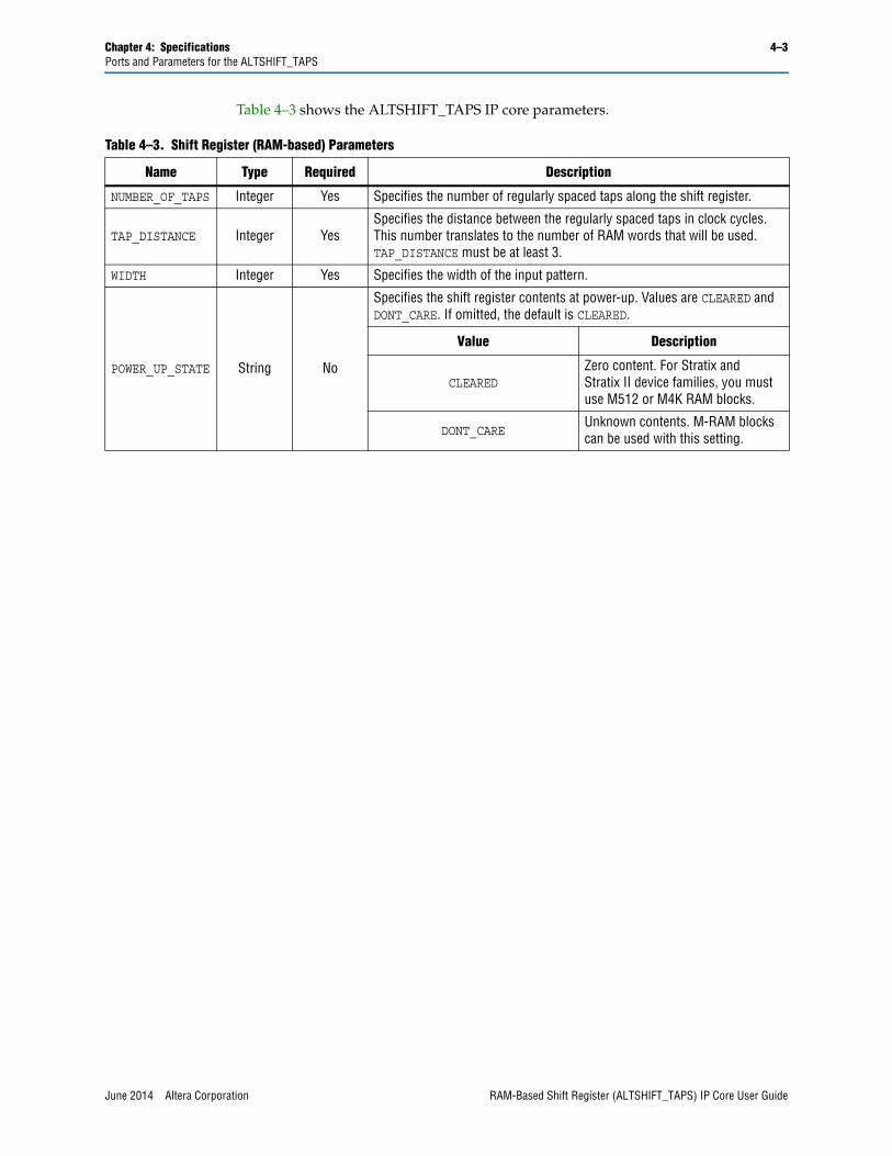
Table 4–3 shows the ALTSHIFT_TAPS IP core parameters.
Table 4–3. Shift Register (RAM-based) Parameters
Name Type Required Description
NUMBER_OF_TAPS Integer Yes Specifies the number of regularly spaced taps along the shift register.
TAP_DISTANCE Integer YesSpecifies the distance between the regularly spaced taps in clock cycles. This number translates to the number of RAM words that will be used. TAP_DISTANCE must be at least 3.
WIDTH Integer Yes Specifies the width of the input pattern.
POWER_UP_STATE String No
Specifies the shift register contents at power-up. Values are CLEARED and DONT_CARE. If omitted, the default is CLEARED.
Value Description
CLEAREDZero content. For Stratix and Stratix II device families, you must use M512 or M4K RAM blocks.
DONT_CAREUnknown contents. M-RAM blocks can be used with this setting.
June 2014 Altera Corporation RAM-Based Shift Register (ALTSHIFT_TAPS) IP Core User Guide

4–4 Chapter 4: SpecificationsPorts and Parameters for the ALTSHIFT_TAPS
RAM-Based Shift Register (ALTSHIFT_TAPS) IP Core User Guide June 2014 Altera Corporation
June 2014 Altera Corporation
5. Design Example
Design Example: Shift Register with TapsThe objective of this design example is to implement and instantiate an ALTSHIFT_TAPS IP core using the IP Catalog and parameter editor. This example uses a shift register with a data width, w, of 8 bits, a taps distance, m, of 3, and the number of taps, n, equal to 4. It also demonstrates how you can tap the data at specific points from the shift register chain.
Design FilesThe example design files are available in the User Guides section on the Literature page of the Altera® website (www.altera.com).
Configuration SettingsRefer to Chapter 2, Using Altera IP Cores to define a shift register function with the following parameters.
Functional Simulation in the ModelSim-Altera SimulatorSimulate the design in the ModelSim®-Altera software to generate a waveform display of the device behavior.
You should be familiar with the ModelSim-Altera software before trying the design example. If you are unfamiliar with the ModelSim-Altera software, refer to the support page for software products on the Altera website (www.altera.com). On the support page, there are links to such topics as installation, usage, and troubleshooting.
Set up and simulate the design in the ModelSim-Altera software by performing the following steps.
1. Unzip the DE_ALTSHIFT_TAPS.zip file to any working directory on your PC.
2. Start the ModelSim-Altera software.
3. On the File menu, click Change Directory.
Table 5–1. Shift Register (RAM-Based) Configuration Settings
Configuration Setting Value
How wide should the ‘shiftin’ input and the ‘shiftout’ output buses be? 8 bits
How many taps would you like? 4
Create groups for each tap output Selected
How wide should the distance between taps be? 3
Create a clock enable port Selected
Create an asynchronous clear port Selected
What should the RAM block type be? Auto
RAM-Based Shift Register (ALTSHIFT_TAPS) IP Core User Guide
5–2 Chapter 5: Design ExampleDesign Example: Shift Register with Taps
4. Select the folder in which you unzipped the files.
5. Click OK.
6. On the Tools menu, click Execute Macro.
7. Select the DE_ALTSHIFT_TAPS.do file and click Open. The DE_ALTSHIFT_TAPS.do file is a script file for the ModelSim-Altera software to automate all the necessary settings for the simulation.
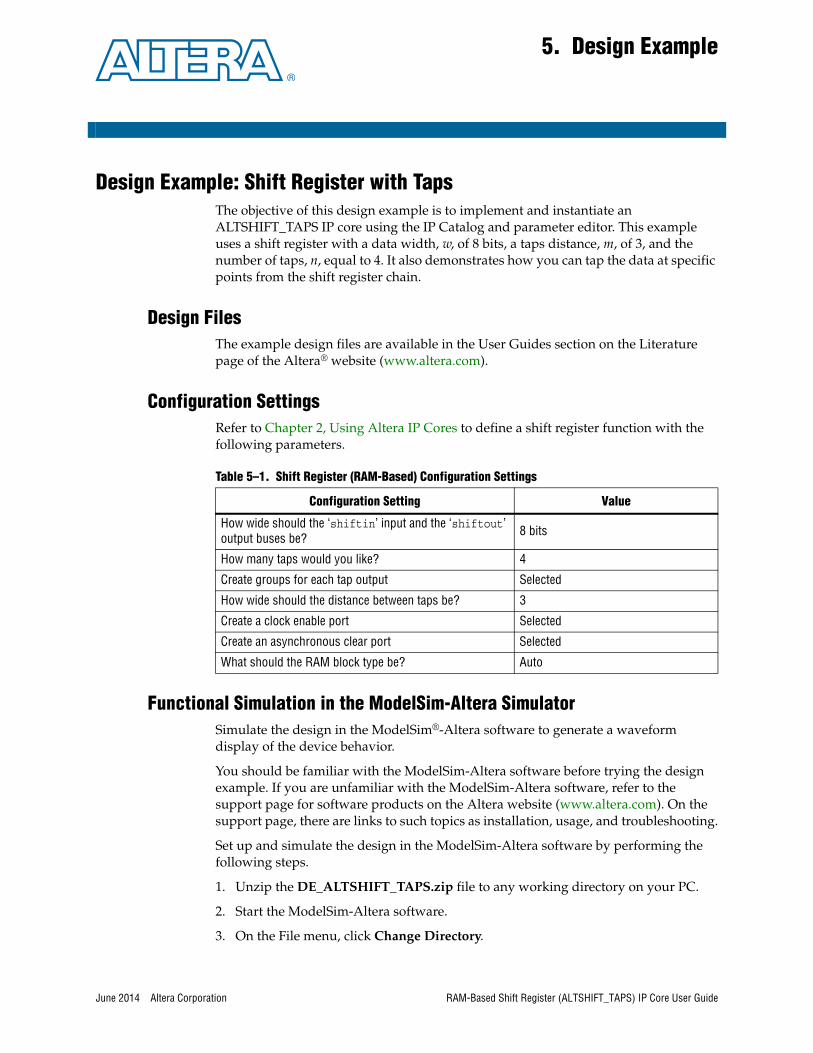
View the simulation results in the Wave window. Figure 5–1 shows the expected simulation results in the ModelSim-Altera software.
Understanding the Simulation ResultsIn this example, you configured the shift register to have the following properties:
■ 8-bit data width
■ Distance between taps (taps length) equals to 3
■ Number of taps equals to 4
■ Created groups for each tap output
■ Created a clock-enable signal and an asynchronous-clear signal
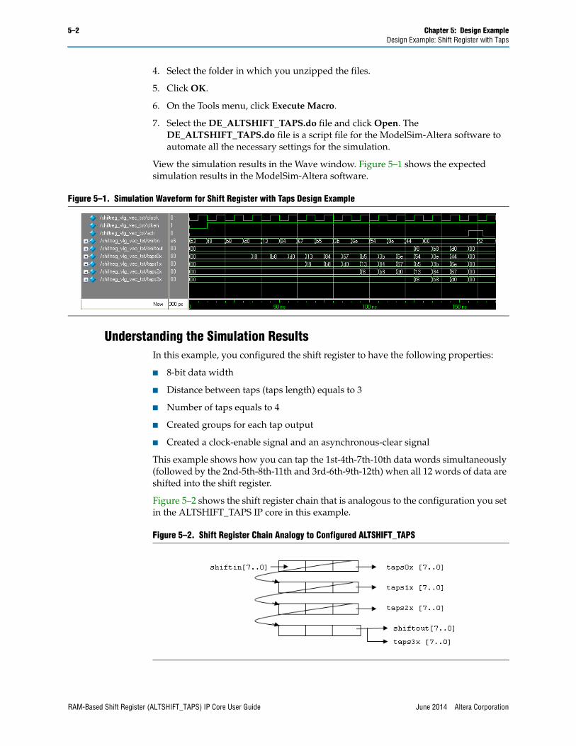
This example shows how you can tap the 1st-4th-7th-10th data words simultaneously (followed by the 2nd-5th-8th-11th and 3rd-6th-9th-12th) when all 12 words of data are shifted into the shift register.
Figure 5–2 shows the shift register chain that is analogous to the configuration you set in the ALTSHIFT_TAPS IP core in this example.
Figure 5–1. Simulation Waveform for Shift Register with Taps Design Example
Figure 5–2. Shift Register Chain Analogy to Configured ALTSHIFT_TAPS
RAM-Based Shift Register (ALTSHIFT_TAPS) IP Core User Guide June 2014 Altera Corporation
Chapter 5: Design Example 5–3Design Example: Shift Register with Taps
The next section uses this shift register chain to explain the shifting operation and the output operation of the ALTSHIFT_TAPS IP core.
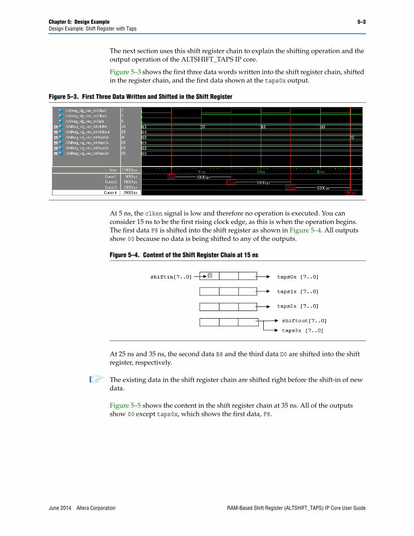
Figure 5–3 shows the first three data words written into the shift register chain, shifted in the register chain, and the first data shown at the taps0x output.
At 5 ns, the clken signal is low and therefore no operation is executed. You can consider 15 ns to be the first rising clock edge, as this is when the operation begins. The first data F8 is shifted into the shift register as shown in Figure 5–4. All outputs show 00 because no data is being shifted to any of the outputs.
At 25 ns and 35 ns, the second data B8 and the third data D0 are shifted into the shift register, respectively.
1 The existing data in the shift register chain are shifted right before the shift-in of new data.
Figure 5–5 shows the content in the shift register chain at 35 ns. All of the outputs show 00 except taps0x, which shows the first data, F8.
Figure 5–3. First Three Data Written and Shifted in the Shift Register
Figure 5–4. Content of the Shift Register Chain at 15 ns
June 2014 Altera Corporation RAM-Based Shift Register (ALTSHIFT_TAPS) IP Core User Guide
5–4 Chapter 5: Design ExampleDesign Example: Shift Register with Taps
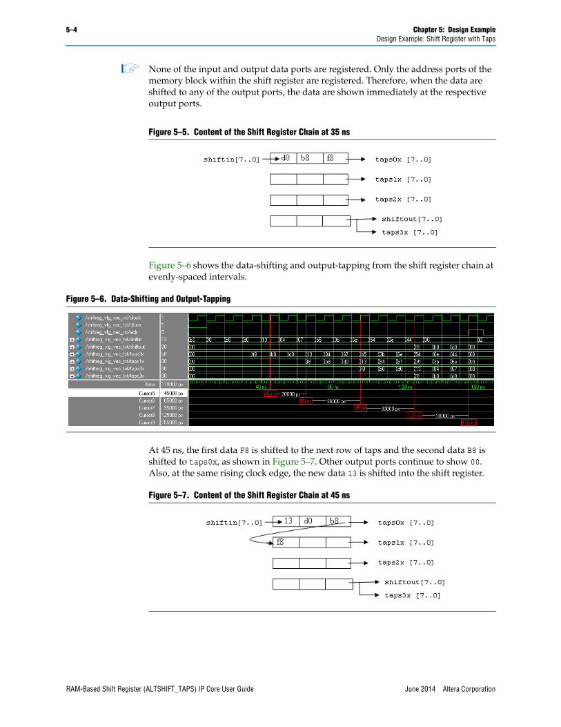
1 None of the input and output data ports are registered. Only the address ports of the memory block within the shift register are registered. Therefore, when the data are shifted to any of the output ports, the data are shown immediately at the respective output ports.
Figure 5–6 shows the data-shifting and output-tapping from the shift register chain at evenly-spaced intervals.
At 45 ns, the first data F8 is shifted to the next row of taps and the second data B8 is shifted to taps0x, as shown in Figure 5–7. Other output ports continue to show 00. Also, at the same rising clock edge, the new data 13 is shifted into the shift register.
Figure 5–5. Content of the Shift Register Chain at 35 ns
Figure 5–6. Data-Shifting and Output-Tapping
Figure 5–7. Content of the Shift Register Chain at 45 ns
RAM-Based Shift Register (ALTSHIFT_TAPS) IP Core User Guide June 2014 Altera Corporation
Chapter 5: Design Example 5–5Design Example: Shift Register with Taps
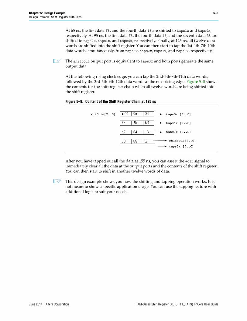
At 65 ns, the first data F8, and the fourth data 13 are shifted to taps1x and taps0x, respectively. At 95 ns, the first data F8, the fourth data 13, and the seventh data B5 are shifted to taps2x, taps1x, and taps0x, respectively. Finally, at 125 ns, all twelve data words are shifted into the shift register. You can then start to tap the 1st-4th-7th-10th data words simultaneously, from taps3x, taps2x, taps1x, and taps0x, respectively.
1 The shiftout output port is equivalent to taps3x and both ports generate the same output data.
At the following rising clock edge, you can tap the 2nd-5th-8th-11th data words, followed by the 3rd-6th-9th-12th data words at the next rising edge. Figure 5–8 shows the contents for the shift register chain when all twelve words are being shifted into the shift register.
After you have tapped out all the data at 155 ns, you can assert the aclr signal to immediately clear all the data at the output ports and the contents of the shift register. You can then start to shift in another twelve words of data.
1 This design example shows you how the shifting and tapping operation works. It is not meant to show a specific application usage. You can use the tapping feature with additional logic to suit your needs.
Figure 5–8. Content of the Shift Register Chain at 125 ns
June 2014 Altera Corporation RAM-Based Shift Register (ALTSHIFT_TAPS) IP Core User Guide

5–6 Chapter 5: Design ExampleDesign Example: Shift Register with Taps
RAM-Based Shift Register (ALTSHIFT_TAPS) IP Core User Guide June 2014 Altera Corporation
June 2014 Altera Corporation
Additional Information
This chapter provides additional information about the document and Altera.
Document Revision HistoryThe following table shows the revision history for this document.
Typographic ConventionsThe following table shows the typographic conventions this document uses.
Date Document Version Changes Made
2014.06.30 3.0
■ Replaced MegaWizard Plug-In Manager information with IP Catalog.
■ Added standard information about upgrading IP cores.
■ Added standard installation and licensing information.
■ Removed outdated device support level information. IP core device support is now available in IP Catalog and parameter editor.
■ Removed all references to obsolete SOPC Builder tool.
May 2013 2.2 Updated to include Arria V, Cyclone V, and Stratix V devices.
November 2010 2.1■ Updated ports and parameters
■ Added prototype and component declarations
July 2008 2.0
■ Updated the list of device families supported by this megafunction
■ Created a new design example with explanations showing the features and behaviors of the megafunction
■ Added the description for the new input pin, aclr
■ Reorganized the whole document
March 2007 1.2 Added Cyclone® III support
December 2006 1.1 Added Stratix® III support
September 2006 1.0 Initial release
Visual Cue Meaning
Bold Type with Initial Capital Letters
Indicate command names, dialog box titles, dialog box options, and other GUI labels. For example, Save As dialog box. For GUI elements, capitalization matches the GUI.
bold typeIndicates directory names, project names, disk drive names, file names, file name extensions, software utility names, and GUI labels. For example, \qdesigns directory, D: drive, and chiptrip.gdf file.
Italic Type with Initial Capital Letters Indicate document titles. For example, Stratix IV Design Guidelines.
RAM-Based Shift Register (ALTSHIFT_TAPS) IP Core User Guide
6–2 Additional InformationTypographic Conventions
italic typeIndicates variables. For example, n + 1.
Variable names are enclosed in angle brackets (< >). For example, <file name> and <project name>.pof file.
Initial Capital Letters Indicate keyboard keys and menu names. For example, the Delete key and the Options menu.
“Subheading Title” Quotation marks indicate references to sections within a document and titles of Quartus II Help topics. For example, “Typographic Conventions.”
Courier type
Indicates signal, port, register, bit, block, and primitive names. For example, data1, tdi, and input. The suffix n denotes an active-low signal. For example, resetn.
Indicates command line commands and anything that must be typed exactly as it appears. For example, c:\qdesigns\tutorial\chiptrip.gdf.
Also indicates sections of an actual file, such as a Report File, references to parts of files (for example, the AHDL keyword SUBDESIGN), and logic function names (for example, TRI).
r An angled arrow instructs you to press the Enter key.
1., 2., 3., anda., b., c., and so on
Numbered steps indicate a list of items when the sequence of the items is important, such as the steps listed in a procedure.
■ ■ ■ Bullets indicate a list of items when the sequence of the items is not important.
1 The hand points to information that requires special attention.
h A question mark directs you to a software help system with related information.
f The feet direct you to another document or website with related information.
c A caution calls attention to a condition or possible situation that can damage or destroy the product or your work.
w A warning calls attention to a condition or possible situation that can cause you injury.
The envelope links to the Email Subscription Management Center page of the Altera website, where you can sign up to receive update notifications for Altera documents.
Visual Cue Meaning
RAM-Based Shift Register (ALTSHIFT_TAPS) IP Core User Guide June 2014 Altera Corporation