Embed Size (px)
Citation preview
Raman spectroscopy of laser inducedmaterial alterations
Dissertation
der Fakultat fur Geowissenschaften
der Ludwig-Maximilians-Universitat
Munchen
vorgelegt von
Michael Bauer
Munchen, den 03. Marz 2010


Erstgutachter: Prof. Dr. Robert W. Stark
Zweitgutachter: Prof. Dr. Wolfgang M. Heckl
Disputation: 06. Juli 2010

Contents
Table of Contents i
List of Figures iii
List of Abbreviations v
Kurzfassung 1
Abstract 2
1 Introduction 3
2 Raman spectroscopy 5
2.1 Interaction of light with matter . . . . . . . . . . . . . . . . . . . . . 5
2.2 The Raman effect . . . . . . . . . . . . . . . . . . . . . . . . . . . . . 6
2.3 Selection rules and Raman line determination . . . . . . . . . . . . . 9
2.4 Influence of stress and temperature on Raman spectra . . . . . . . . . 10
3 Methods 17
3.1 The confocal Raman microscope set up . . . . . . . . . . . . . . . . . 17
3.1.1 Pinhole influence and light suppression . . . . . . . . . . . . . 18
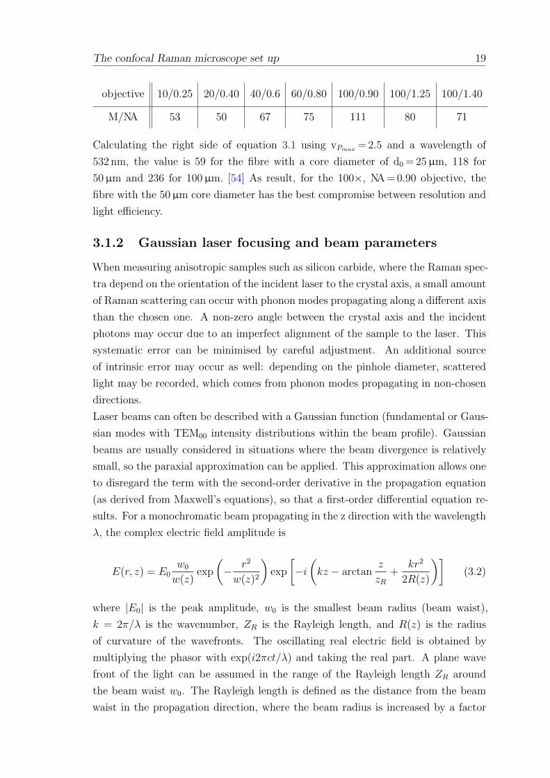
3.1.2 Gaussian laser focusing and beam parameters . . . . . . . . . 19
3.2 Local heating due to the focused laser beam . . . . . . . . . . . . . . 21
3.3 Image generation . . . . . . . . . . . . . . . . . . . . . . . . . . . . . 21
4 Spectroscopic characterisation 23
4.1 Silicon . . . . . . . . . . . . . . . . . . . . . . . . . . . . . . . . . . . 23
4.1.1 Phonon dispersion curve and band structure . . . . . . . . . . 23
4.1.2 Raman scattering in silicon . . . . . . . . . . . . . . . . . . . 25
4.1.3 Local heating . . . . . . . . . . . . . . . . . . . . . . . . . . . 26
4.1.4 Experimental results . . . . . . . . . . . . . . . . . . . . . . . 27
4.2 Silicon carbide . . . . . . . . . . . . . . . . . . . . . . . . . . . . . . . 27
i
ii Table of Contents
4.2.1 Crystal structure and polytypes . . . . . . . . . . . . . . . . . 28
4.2.2 Phonon structure and mode folding . . . . . . . . . . . . . . . 29
4.2.3 Raman line shift . . . . . . . . . . . . . . . . . . . . . . . . . 31
4.2.4 Local heating . . . . . . . . . . . . . . . . . . . . . . . . . . . 32
4.2.5 Experimental results . . . . . . . . . . . . . . . . . . . . . . . 33
4.3 Alteration of calcium fluoride caused by UV-light . . . . . . . . . . . 34
4.3.1 Material properties of calcium fluoride . . . . . . . . . . . . . 36
4.3.2 Identification of kerogeneous carbon . . . . . . . . . . . . . . . 37
4.3.3 Experimental results . . . . . . . . . . . . . . . . . . . . . . . 38
4.4 Titanomagnetites . . . . . . . . . . . . . . . . . . . . . . . . . . . . . 39
5 Summary 43
6 References 45
7 Publications 55
7.1 Visualizing stress in silicon microcantilevers using scanning confocal
Raman spectroscopy . . . . . . . . . . . . . . . . . . . . . . . . . . . 55
7.2 Temperature depending Raman line-shift of silicon carbide . . . . . . 61
7.3 Nanoscale residual stress-field mapping around nanoindents in SiC by
IR s-SNOM and confocal Raman microscopy . . . . . . . . . . . . . . 71
7.4 Exterior surface damage of calcium fluoride out coupling mirrors for
DUV lasers . . . . . . . . . . . . . . . . . . . . . . . . . . . . . . . . 81
7.5 Onset of the optical damage in CaF2 optics caused by deep-UV lasers 95
Appendix I
Acknowledgements XV
Curriculum Vitae XVI
Publication list XVII
List of Figures
2.1 Typical configuration of IR and Raman spectroscopy . . . . . . . . . 6
2.2 Jablonksi energy diagram of the scattering processes . . . . . . . . . . 7
3.1 Schematic of the confocal setup . . . . . . . . . . . . . . . . . . . . . 17
3.2 Lateral resolution of a scattering point as a function of detector size . 18
3.3 Illustrated Gaussian beam of a focused laser beam . . . . . . . . . . . 20
3.4 Filter region for sum filtering and Lorentz fits . . . . . . . . . . . . . 22
4.1 Electronic band structure and phonon dispersion curves of silicon . . 24
4.2 Refraction and extinction index of silicon with penetration depth and
adsorption . . . . . . . . . . . . . . . . . . . . . . . . . . . . . . . . . 24
4.3 Variation of peak centre and peak width due to local heating . . . . . 26
4.4 Measurements of a silicon AFM cantilever . . . . . . . . . . . . . . . 27
4.5 Side view ABC layer stacking and of silicon carbide . . . . . . . . . . 29
4.6 Phonon dispersion curve of silicon carbide . . . . . . . . . . . . . . . 30
4.7 Mode folding of silicon carbide . . . . . . . . . . . . . . . . . . . . . . 30
4.8 Raman spectra of silicon carbide . . . . . . . . . . . . . . . . . . . . . 31
4.9 Temperature-induced peak shift and increasing peak width of silicon
and silicon carbide . . . . . . . . . . . . . . . . . . . . . . . . . . . . 33
4.10 Temperature-dependent shifting of peak centres and stress fields
around a nanoindentation in SiC . . . . . . . . . . . . . . . . . . . . 33
4.11 Layer materials used for ultraviolet optical components . . . . . . . . 35
4.12 First- and second-order Raman spectra of kerogen carbon . . . . . . . 37
4.13 Damage structure due to UV photon irradiation . . . . . . . . . . . . 39
4.14 Raman spectra of synthetic magnetite and titanomagnetite . . . . . . 40
4.15 Titanium concentration against laser power for beginning material
alteration . . . . . . . . . . . . . . . . . . . . . . . . . . . . . . . . . 41
4.16 Stripes of different titanomagnetites in a geologic sample . . . . . . . 42
iii

iv List of Figures
List of Abbreviations
AFM atomic force microscopeArF argon fluorideCaF2 calcium fluorideCaCO3 calcium carbonateCCD charge coupled deviceDUV deep ultravioletFLA folded longitudinal acoustic phononFLO folded longitudinal optical phononFTA folded transversal acoustic phononFTO folded transversal optical phononFWHM full width at half maximumHR high reflective (mirror)IR infraredKrF krypton fluorideLA longitudinal acoustic phononLO longitudinal optical phononLOPC LO-phonon plasmon coupledMEMS micro(electro) mechanical systemsMgF2 magnesium fluorideNA numerical apertureNd:YAG neodymium doped yttrium aluminium garnetOC out coupling (mirror)PDP phonon deformation potentialPSF point spread functionSi siliconSiC silicon carbideSHG second harmonic generations-SNOM scattering scanning nearfield optical microscopeTA transversal acoustic phononTEM transverse electro magnetic (laser);
or transmission electron microscopeTO transversal optical phononUV ultravioletVUV vacuum ultraviolet
v

vi List of Abbreviations
Kurzfassung 1
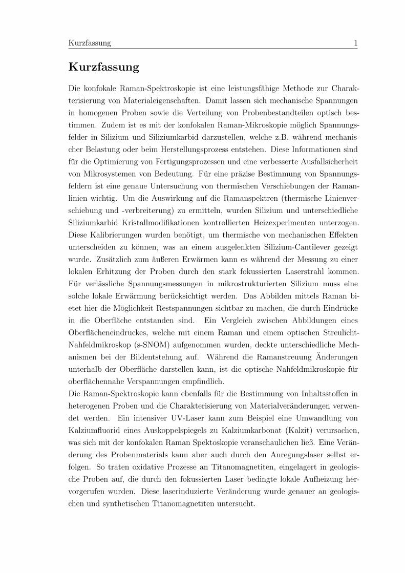
Kurzfassung
Die konfokale Raman-Spektroskopie ist eine leistungsfahige Methode zur Charak-
terisierung von Materialeigenschaften. Damit lassen sich mechanische Spannungen
in homogenen Proben sowie die Verteilung von Probenbestandteilen optisch bes-
timmen. Zudem ist es mit der konfokalen Raman-Mikroskopie moglich Spannungs-
felder in Silizium und Siliziumkarbid darzustellen, welche z.B. wahrend mechanis-
cher Belastung oder beim Herstellungsprozess entstehen. Diese Informationen sind
fur die Optimierung von Fertigungsprozessen und eine verbesserte Ausfallsicherheit
von Mikrosystemen von Bedeutung. Fur eine prazise Bestimmung von Spannungs-
feldern ist eine genaue Untersuchung von thermischen Verschiebungen der Raman-
linien wichtig. Um die Auswirkung auf die Ramanspektren (thermische Linienver-
schiebung und -verbreiterung) zu ermitteln, wurden Silizium und unterschiedliche
Siliziumkarbid Kristallmodifikationen kontrollierten Heizexperimenten unterzogen.
Diese Kalibrierungen wurden benotigt, um thermische von mechanischen Effekten
unterscheiden zu konnen, was an einem ausgelenkten Silizium-Cantilever gezeigt
wurde. Zusatzlich zum außeren Erwarmen kann es wahrend der Messung zu einer
lokalen Erhitzung der Proben durch den stark fokussierten Laserstrahl kommen.
Fur verlassliche Spannungsmessungen in mikrostrukturierten Silizium muss eine
solche lokale Erwarmung berucksichtigt werden. Das Abbilden mittels Raman bi-
etet hier die Moglichkeit Restspannungen sichtbar zu machen, die durch Eindrucke
in die Oberflache entstanden sind. Ein Vergleich zwischen Abbildungen eines
Oberflacheneindruckes, welche mit einem Raman und einem optischen Streulicht-
Nahfeldmikroskop (s-SNOM) aufgenommen wurden, deckte unterschiedliche Mech-
anismen bei der Bildentstehung auf. Wahrend die Ramanstreuung Anderungen
unterhalb der Oberflache darstellen kann, ist die optische Nahfeldmikroskopie fur
oberflachennahe Verspannungen empfindlich.
Die Raman-Spektroskopie kann ebenfalls fur die Bestimmung von Inhaltsstoffen in
heterogenen Proben und die Charakterisierung von Materialveranderungen verwen-
det werden. Ein intensiver UV-Laser kann zum Beispiel eine Umwandlung von
Kalziumfluorid eines Auskoppelspiegels zu Kalziumkarbonat (Kalzit) verursachen,
was sich mit der konfokalen Raman Spektoskopie veranschaulichen ließ. Eine Veran-
derung des Probenmaterials kann aber auch durch den Anregungslaser selbst er-
folgen. So traten oxidative Prozesse an Titanomagnetiten, eingelagert in geologis-
che Proben auf, die durch den fokussierten Laser bedingte lokale Aufheizung her-
vorgerufen wurden. Diese laserinduzierte Veranderung wurde genauer an geologis-
chen und synthetischen Titanomagnetiten untersucht.
2 Abstract
Abstract
Confocal Raman spectroscopy is a powerful tool for material characterisation. It can
be used for the optical characterisation of mechanical stress in homogeneous samples,
for material identification, and for compositional mapping. In addition, confocal Ra-
man microscopy is useful for the measurement of stress fields generated, for example,
by mechanical loading or residual stress after fabrication in silicon and silicon car-
bide. This information is important for optimising manufacturing processes and
increasing the reliability of micro devices. For precise stress measurements, the
thermally induced shift of Raman peaks must be characterised in detail. For that
purpose, silicon and different silicon carbide polytypes underwent controlled heating
experiments to determine the effect of heating on Raman spectra (thermal peak shift
and increasing line width). These calibrations are required to separate effects caused
by temperature changes from those caused by mechanical stress. The separation of
stress- and temperature-induced effects was demonstrated for the measurement of
stress fields in a deflected silicon cantilever. In addition to external heating, the mea-
surement itself may affect the sample temperature because the focused, intense light
can locally heat the sample. Local heating must be taken into account to ensure
reliable stress measurements in silicon micro-structures. Raman mapping may also
be used to characterise residual stress fields caused by nanoindentation. A compari-
son between Raman mapping and scattering scanning near-field optical microscopy
(s-SNOM) of a nanoindentation imprint in silicon carbide revealed subtle differences
in the imaging mechanisms. Scattering-SNOM is sensitive to near surface stress,
whereas Raman scattering can reveal sub-surface changes.
Raman spectroscopy can also be used for compositional mapping of heterogeneous
specimens or for the characterisation of material alterations. For example, intense
UV-laser light may induce the alteration from calcium fluorite to calcium carbonate
(calcite) in outcoupling mirrors. These alterations can be visualised by confocal
Raman microscopy. Material alterations can also be caused by the excitation laser
itself. During the investigation of titanomagnetites that were embedded in geologic
samples, oxidative processes occurred and they were driven by local heating due
to the focused laser. The laser-induced alterations were investigated in detail on
geologic and synthetic titanomagnetite samples.
1 Introduction
Compositional mapping or quantitative chemical analysis is important in micro- and
nanostructured materials. In addition to other techniques, including atomic force
microscopy (AFM) and scanning electron microscopy (SEM), Raman spectroscopy
is becoming an increasingly common analysis method. It offers fast and contact-free
measurements with easy sample preparation. Raman spectroscopy is a vibrational
spectroscopy method that is based on the analysis of inelastically scattered light.
The incident photons scatter off molecular vibrations (e.g., bending and rotational
vibrations) or, in the case of crystals, off phonons (e.g., different modes of lattice
vibration. As a result, specific spectral peak shifts occur, providing highly sensitive
measurements of the material. The spectra consist of peaks that are unique in
their position, shape and intensity. [1, 2] Usually, lasers are used as monochromatic
excitation sources and the so-called Raman shift, i.e., the energy loss (or gain) of
the scattered light, is given.
Raman spectroscopy can be used on a heterogeneous specimen to determine its com-
position. The spatial resolution is restricted only by the scattering volume. With
a confocal set-up, the scattering volume can be controlled, allowing compositional
mapping with sub-micrometer resolution. This sensitivity allows material composi-
tion questions to be answered with Raman spectroscopy. [1, 2]
In addition to sample composition, other parameters such as residual stress or tem-
perature can be quantified with Raman spectroscopy. [3–5] Mechanical stress affects
the phonon frequencies, which can be recognised as additional shifts of the Raman
spectral peaks. With the continuing reduction of feature size in small devices such as
micro-electro-mechanical systems (MEMS), stress fields in devices are becoming in-
creasingly important. [3] One result of this continuing miniaturisation is the increase
of mechanical stress in device structures. Different thermal expansion coefficients
of different materials may induce mechanical stresses along structural edges and at
corners during device operation. Monitoring these stresses is important to improve
device reliability and to increase fabrication yield. In addition to mechanical stresses,
temperature also affects a material’s phonon scattering properties. The population
of phonon modes increases with increasing temperature, and a variation in the pop-
3
4 Introduction
ulation is expressed as a change in the peak width. Analysing the peak width allows
one to measure the sample temperature optically.
Because confocal Raman spectroscopy uses a focused laser, the temperature in the
scattering volume may increase significantly. Depending on the thermal conductivity
and light reflectivity of the sample, it will be locally heated to some degree, which
can affect the phonons directly. This local heating effect must be compensated for
in stress measurements. The local laser heating may also induce material alterations
or even induce the destruction of the sample. [6, 7]
In the thesis, the following issues will be discussed. The thesis starts in chapter 2 with
the theoretical background of the Raman effect, explaining the selection rules for
the scattering process. The influences of mechanical stress and varying temperature
on Raman spectra are also briefly discussed. Chapter 3 describes the measurement
system and explains the components and their influences on measurements. The
spectroscopic characteristics of the materials are summarised in chapter 4. Impor-
tant experimental results include the dependency of the spectra on mechanical stress
and temperature in silicon and silicon carbide single crystals. Compositional map-
ping is shown for the failure analysis of calcium fluoride resonator mirrors impaired
from high flux ultraviolet photons. Titanomagnetites particles, which are embedded
in a deep sea basalt specimen, are a further example for chemical analysis. A con-
cluding summary is given in chapter 5. The results that were published in scientific
journals are provided in chapter 7.
2 Raman spectroscopy
Raman spectroscopy records the highly specific vibrational fingerprint of a material
by analysing inelastically scattered light. Raman spectroscopy is based on the Ra-
man effect, which was named after the Indian physicist Chandrasekhara Venkata
Raman, who found in 1928”A new type of secondary radiation“. [8] Independently,
the same observation was reported by Landside and Mandelbaum. [9] With the de-
velopment of intense single mode lasers as powerful monochromatic light sources,
the Raman effect became widely used in science and engineering. Confocal Raman
spectroscopy has an intrinsic”nano-specificity“because it probes vibrations of chem-
ical bonds and the propagation phonons in a small sample volume, typically less
than 1µm3.
Vibrational stretching modes are highly characteristic for specific chemical bonds
and often allow for compositional identification. In general, vibrational bending
modes are more sensitive to the neighbouring entities and, hence, to the molecular
short-range order. Librational and external modes, which depend on the structure,
involve relative motions of entire units of molecules or atoms. Well-defined repetitive
structures in crystals typically give rise to Raman spectra with sharp and well-
resolved peaks. Spectra with broad bands indicate that different configurations or
many electric or mass defects may exist in the crystal. Thus, if the proportion of
atoms belonging to the (near-) surface region of the probed volume is significant,
the disorder related to the various atomic arrangements contributes to the observed
Raman features. [10]
2.1 Interaction of light with matter
Various processes can occur when light interacts with matter. In a case where the
photon energy matches the difference between two real states of a molecule, the
molecule can be excited into a higher electronic state. The excited molecule can
relax to the ground state via a non-radiative process or via an additional luminous
process (fluorescence). This process is used in absorption spectroscopy techniques
such as infra-red (IR) spectroscopy. If the photon energy does not match the differ-
5
6 Raman spectroscopy
ence between the current state and another real state, it can be scattered inelastically
(Brillouin and Raman scattering) or elastically (Rayleigh and Mie scattering). For
an elastically scattered photon, the photon energy (wavelength) is the same before
and after the scattering process. The process can be considered absorption of the
photon (excitation of matter into a virtual intermediate state), which is followed by
a prompt relaxation with re-emission of the photon. In contrast, inelastic Raman
scattering is a nonlinear scattering process, involving quasiparticles such as phonons
in a lattice or molecular vibrations (e.g., bending or rotation). [11–13] The amount
of energy change (either loss or gain) by a photon is characteristic for the nature
of vibration (phonon or chemical bond). Nevertheless, not all vibrations will be ob-
servable with Raman spectroscopy because Raman scattering depends on symmetry
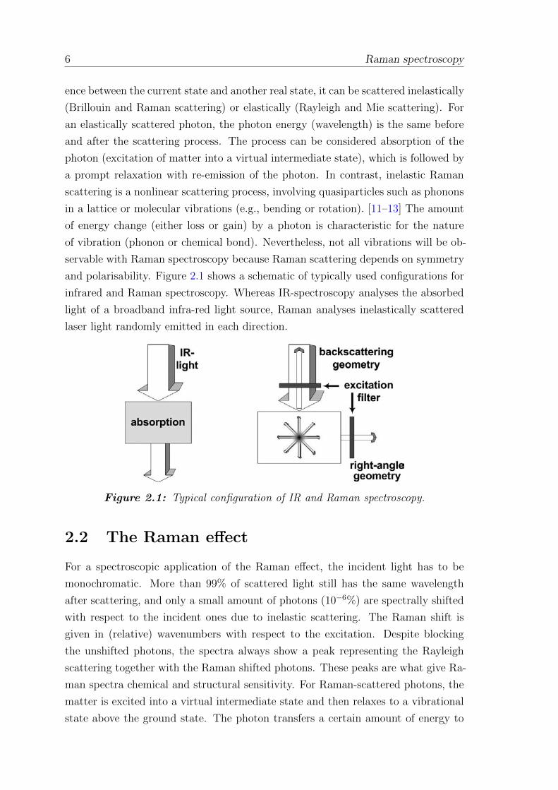
and polarisability. Figure 2.1 shows a schematic of typically used configurations for
infrared and Raman spectroscopy. Whereas IR-spectroscopy analyses the absorbed
light of a broadband infra-red light source, Raman analyses inelastically scattered
laser light randomly emitted in each direction.
Figure 2.1: Typical configuration of IR and Raman spectroscopy.
2.2 The Raman effect
For a spectroscopic application of the Raman effect, the incident light has to be
monochromatic. More than 99% of scattered light still has the same wavelength
after scattering, and only a small amount of photons (10−6%) are spectrally shifted
with respect to the incident ones due to inelastic scattering. The Raman shift is
given in (relative) wavenumbers with respect to the excitation. Despite blocking
the unshifted photons, the spectra always show a peak representing the Rayleigh
scattering together with the Raman shifted photons. These peaks are what give Ra-
man spectra chemical and structural sensitivity. For Raman-scattered photons, the
matter is excited into a virtual intermediate state and then relaxes to a vibrational
state above the ground state. The photon transfers a certain amount of energy to
The Raman effect 7
the material, losing energy (Stokes shift). If the matter is already in a vibrationally
excited state, inelastically scattered photons may also gain energy. The incident
photon excites the material to a virtual intermediate state, which then can relax to
its ground state. The scattered photon gains the energy difference, having a higher
energy than before the scattering event (anti-Stokes shift). These three Raman scat-
tering processes can be understood in a classical picture as a collision between the
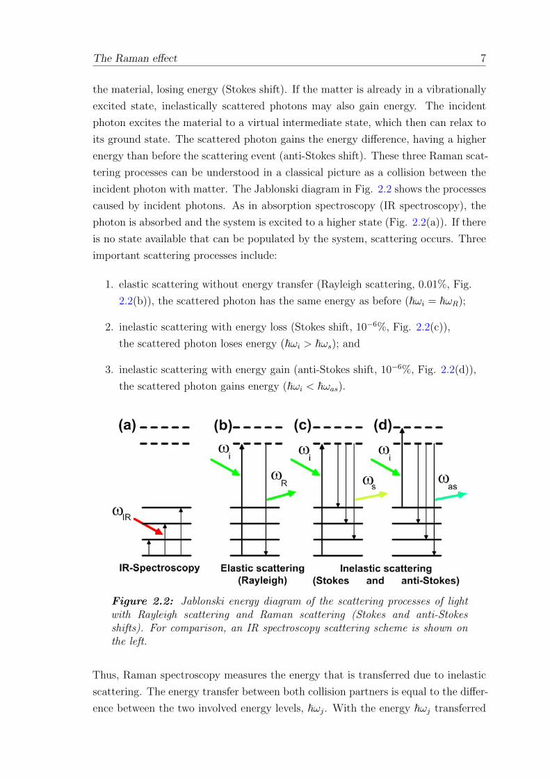
incident photon with matter. The Jablonski diagram in Fig. 2.2 shows the processes
caused by incident photons. As in absorption spectroscopy (IR spectroscopy), the
photon is absorbed and the system is excited to a higher state (Fig. 2.2(a)). If there
is no state available that can be populated by the system, scattering occurs. Three
important scattering processes include:
1. elastic scattering without energy transfer (Rayleigh scattering, 0.01%, Fig.
2.2(b)), the scattered photon has the same energy as before (~ωi = ~ωR);
2. inelastic scattering with energy loss (Stokes shift, 10−6%, Fig. 2.2(c)),
the scattered photon loses energy (~ωi > ~ωs); and
3. inelastic scattering with energy gain (anti-Stokes shift, 10−6%, Fig. 2.2(d)),
the scattered photon gains energy (~ωi < ~ωas).
Figure 2.2: Jablonski energy diagram of the scattering processes of lightwith Rayleigh scattering and Raman scattering (Stokes and anti-Stokesshifts). For comparison, an IR spectroscopy scattering scheme is shown onthe left.
Thus, Raman spectroscopy measures the energy that is transferred due to inelastic
scattering. The energy transfer between both collision partners is equal to the differ-
ence between the two involved energy levels, ~ωj. With the energy ~ωj transferred
8 Raman spectroscopy
during the scattering process and the energy ~ωi before scattering, the scattered
photon will have the energy
~ωs/as = ~ωi ∓ ~ωj. (2.1)
The plus and minus in equation 2.1 stand for the energy gain (anti-Stokes shift) or
energy loss (Stokes) of the photon. The Stokes and anti-Stokes shifts are symmetric,
determined by the difference of energy between the ground state and the vibrational
state.
For scattering on molecules, the electric field of the photon affects the molecule’s
electrons, resulting in molecular distortion. The distorted molecule acquires a con-
tribution to its dipole moment µ (even if initially non-polar):
µ = αE (2.2)
where α is a proportional constant of molecule’s polarisability. The polarisability
corresponds to the ease with which the electron cloud around a molecule can be
distorted. The induced dipole can emit or scatter light at the optical frequency of
the incident light wave. Vibrational Raman scattering occurs because a molecular
vibration can change the polarisability. The change is described by the polarisability
derivative, ∂a/∂Q, where Q is the normal coordinate of the vibration. The polar-
isability is typically different if the field is applied parallel or perpendicular to the
molecular axis or in different directions relative to the molecule. Nevertheless, for
a small electric field, the polarisability is the same for the field oriented in opposite
directions along the same axis (µ(−E) = −µ(E)).
Thus, the distortion induced in a molecule by an applied electric field depends on the
relative orientation and returns to its initial value after a rotation of 180. The selec-
tion rules for Raman-active vibrations are linked to molecular symmetry and iden-
tify vibrations that change a molecule’s polarisability. For scattering on anisotropic
crystals, with the propagating phonons dependent on the crystal axis, a similar de-
pendence to the orientation of the light to the crystal axis is distinguishable. Raman
peaks were observable within the spectra, depending on the scattering geometry.
The features of one phonon contributing to Raman scattering, incipient next to
the Rayleigh peak, were followed by higher order scattered peaks in the spectra,
involving multiple phonons (in the second-ordered peaks, two phonons participate).
The peak intensity decreases with increasing number of participating phonons.
The population of present elementary oscillations gives the efficiency of the anti-
Stokes process, proportional to the Boltzmann distribution. The stronger of the two
processes is by far Stokes scattering because the population state is dominated by
its vibrational state at room temperature. Most Raman techniques investigate the
Stokes photons only, while ignoring the anti-Stokes photons.
Selection rules and Raman line determination 9
2.3 Selection rules and Raman line determination
Selection rules allow one to predict if a certain molecular or lattice vibration oscilla-
tion is Raman or IR active. The selection rules for Raman scattering are analogous
to those for infrared-active vibrations, which state that there must be a change in the
permanent dipole moment µ during the vibration. In contrast to IR spectroscopy, the
Raman active normal vibrations change the polarisability α. Group theory methods,
called nuclear site group analysis, show that for a molecular symmetry centre, the
Raman-active vibrations will be silent in the infrared and vice versa. [11, 12, 14, 15]
Because of the requirement of a conserved total angular momentum in the ground
state of the system, only certain transitions can be induced. A basic summary and
tables are given in the book by W. J. Miller. [15]
The IR intensity is proportional to the square of the variation of the dipole moment
µ, whereas the Raman intensity is proportional to the square of the change in the
polarisability α:
IIR ∝(∂µ
∂q
)2
0
, IRaman ∝(∂α
∂q
)2
0
. (2.3)
Here, q is the normal coordinate of the vibration.
In crystals, the interaction between the incident photon and a phonon is indirect.
The interaction is connected to electronic interband transitions, which determine the
dielectric susceptibility χ in the visible spectral range. [16] If these interband transi-
tions are influenced by phonons, Raman scattering occurs. The normal coordinate
of a phonon can be expressed classically as
Qj = Aje[±i(qj · r−Qj · t)]. (2.4)
The vibrational influence on the susceptibility tensor can be described by expanding
χ into a Taylor series with respect to the normal coordinate of the vibration Qj:
χ = χ(0) +∑j
χ(1)Qj + ... = χ0 +∑j
(∂χ
∂Qj
)0
Qj + ... (2.5)
The summation runs over the 3N − 3 vibrational modes, with N as the number
of atoms in the unit cell. [16] For example, for the diatomic base of silicon, the
summation runs over the three optical phonons; for SiC, the summation depends on
the individual polytype.
If monochromatic light with the frequency ωi illuminates a sample in the direction
ki, the associated electric field E induces an electric moment P according to
10 Raman spectroscopy
P = ε0χE = ε0χE0e[i(ki · r−ωit)]. (2.6)
Combining equation (2.4) and (2.6) results in
P = ε0χ0E +∑j
ε0AjE0
(∂χ
∂Qj
)0
e[i(ki±qj) · r−i(ωi±ωj)t]. (2.7)
The first term represents Rayleigh scattering. The second term corresponds to Stokes
and anti-Stokes scattering with the frequencies ωi ± ωj. This second term can only
be observed if there is a change in dielectric susceptibility (∂χ/∂ωj)0 = χ(1) 6= 0.
Higher order terms in the Taylor expansion describe multi-phonon processes leading
to higher order Raman scattering. The elements of χ(1) are often referred to as
components of the Raman tensor determining a normal vibration Qj as Raman
active or not. [3, 16] The exact form of the Raman tensor depends on the crystal
symmetry as described by W. Hayes [17] and Rousseau et al. [18] For example, in
the orthonormal coordinate system x = [100], y = [010] and z = [001], the Raman
tensors for silicon have the form: [3, 16]
Rx =
0 0 00 0 d0 d 0
, Ry =
0 0 d0 0 0d 0 0
, Rz =
0 d 0d 0 00 0 0
(2.8)
The entire Raman scattering efficiency I is then given by
I = C ·∑j
|eiRjes|2 (2.9)
where ei and es are the polarization vectors of the incident and scattered light,
respectively, C is a constant. [3, 16]
2.4 Influence of stress and temperature on Ra-
man spectra
Mechanical and residual stress in semiconductor materials plays an important role in
the design and reliability of devices. For example, stress can increase the probability
of device failure after fabrication or during operation. Devices are often made of dif-
ferent materials, usually with different thermal expansion coefficients. Mechanical
stress can develop in thin films and substrates, especially at the material interfaces
of embedded structures. [19] Bi- and uniaxial stresses inside the material may be
caused for various reasons: lattice mismatch at the interface of different materials,
Influence of stress and temperature on Raman spectra 11
thermal mismatch due to different thermal expansion coefficients, or volume expan-
sion or internal stress of different material layers deposited or grown on the substrate
during device processing. Stress may directly trigger the nucleation and propagation
of dislocations, generated at points with very high local stress, and the formation
of cracks and voids. [20] Furthermore, stress has an important influence on dopant
diffusion. Stress can cause hot carrier degradation and boron segregation into ar-
eas with dislocation loops. [3, 21] Controlling residual strain by strain engineering,
however, allows the manipulation of free carrier mobility in semiconductors. For
example, hole mobility may be increased by 200%. [22] In general, strain engineer-
ing may enable manipulation of electronic properties at the nanoscale, leading to
custom and specialised devices. [22]
For crystalline materials, Raman spectra depend on the phonon band structure
of the lattice. [3, 12, 14, 16, 17] Direct measurement of the phonon band structure
can be provided by Raman spectroscopy, e.g., for silicon and silicon carbide single
crystals. [3,16,23,24] The phonon frequencies change with external influences, such
as mechanical stress and strain. The resultant displacement of atoms changes the
phonon frequencies, as indicated by shifted Raman peak centres. [3,5,16,25,26] The
relation between strain ε and stress σ is given by Hooke’s law, σ = cε where the
elastic modulus c, represents the stiffness of the system. The strain is proportional
to the applied stress and implies that the system can be treated as a harmonic
oscillator. [26] The effect of strain on the Raman-active optical phonons of crystalline
materials has been studied quite extensively since the 1970s. For a given stress,
the difference ωj between each Raman frequency ω0 can be calculated from the
eigenvalues λj
λj = ω2j − ω2
j0 or ∆ωj = ωj − ωj0 ≈λj
2ωj0
(2.10)
with j = 1, 2, 3 for the given stress and j = 0 without stress. [3] Each of the split
phonons exhibits its own frequency, which varies linearly with the components in
the elastic regime. Observation of a shift may therefore be attributed to a tensile
or compressive strain present in the scattering volume for moderate changes. In
summary, the relation between the measured Raman shift and uniaxial stress is
then obtained to be
∆ω =1
ω0
(pS12 + q(S11 + S12))σ0. (2.11)
The elastic constant Sij is a matrix element of the elastic compliance tensor S, and
p and q come from the phonon deformation potentials (PDPs), all of which are
material properties. [16,26] Optical phonons are influenced by strain in the material
via the phonon deformation potentials. The amount of stress σ is determined via
12 Raman spectroscopy
the elasticity constants from external or internal stress according to Hooke’s law
εij = Sijσ (where εij is the strain tensor component). Compressive stress (σ < 0)
leads to a positive shift (∆ω > 0), whereas tensile stress (σ > 0) shifts to lower
wavenumbers (∆ω < 0).
The theoretical background of the influence of mechanical stress on optical phonon
modes in silicon is described in detail in the dissertation of Dombrowski [16] and the
review of De Wolf. [3] The morphic effects of stress on the optical phonon modes
of silicon were addressed by Ganesan [27] and Anastassakis [28]. In the presence
of a symmetric strain, the triple degeneracy of the k = 0 optical silicon phonon
with frequency is lifted due to anisotropic changes in the lattice constants. [3] For
uniaxial or biaxial stress, the shift can be obtained theoretically. [29] According to
the literature, the value of the constant in Eq. 2.12 was determined to be -434
or -518. [19, 30] As result, the relation measured on a (110) silicon surface can be
written as follows
σ (MPa) ≈ C ·∆ω (cm−1) σ (MPa) = −434∆ω (cm−1) uniaxial (2.12)
σxx + σyy (MPa) = −434∆ω (cm−1) biaxial.
Mechanical stress leads to a change in the phonon frequency but should not influence
the phonon lifetime (no peak broadening). [31] Line broadening due to mechanical
stress is negligible because the phonon population density remains approximately
static for moderate stresses. [26,32,33] However, high mechanical stress can slightly
influence the phonon occupation. [34–36] The line width is expected to reveal the
influence of the phonon dispersion on decay processes due to the changes in the
phonon frequency throughout the Brillouin zone. [26] The mechanical component of
the measured peak shift correlates with the elastic deformation of the crystal lattice
and is mainly independent of temperature. [32] The transverse optical phonons, in
contrast, remain unchanged with increasing pressure. [34,37–40]
The Raman peak centre (frequency) not only depends on mechanical stress (σ)
or strain (ε) but also depends on the local sample temperature (T) because the
interatomic distance changes due to thermal expansion. With a linear expansion
of the equilibrium position of the atoms caused by thermal expansion, the effective
bond strength changes, modifying the phonon frequencies. As a result, the Raman
peak position is a function of strain and stress as well as temperature. The influence
of temperature on the Raman spectra of wurtzite-type crystals was investigated
in 1977 by Mead et al. [4] The temperature-dependent function for the phonon
confinement can be given as
ω(q, T ) = ω(q) + ∆ω1(T ) + ∆ω2(T ). (2.13)
Influence of stress and temperature on Raman spectra 13
Here, ∆ω1(T ) corresponds to the frequency shift due to phonon decay processes of
phonon-phonon coupling and ∆ω2(T ) indicates the frequency shift due to thermal
expansion of the crystal lattice. [41] For example, investigations of the thermal ex-
pansion anisotropy of SiC show nonlinear changes in thermal expansion with temper-
ature, thereby causing variation of the lattice parameter in different directions. [42]
Following general temperature behaviour, for processes in which one phonon i is
destroyed and two phonons j are generated or two phonons i are destroyed and one
phonon j is created, one obtains:
ωi(T ) = ωi(T = 0)−∑j
BijNj(T ), with Nj =1
exp(~ωj
kBT)− 1
(2.14)
with Nj as the phonon occupation of the j-th mode. The term Bij contains phonon
frequencies and anharmonic coefficients for mode i, mode j and i−j cross terms. [43]
The temperature dependence of optical phonons can be distinguished between two
ways. First, the phonon frequencies become altered due to thermal expansion, re-
sulting in what is called an ’implicit effect’ (∆ω2(T ) in Eq. 2.13), obtained from
the volume dependence of the phonon frequencies. [43, 44] Second, there are also
shifts in phonon frequencies arising from higher order terms (e.g., cubic, quadratic,
etc.) in the crystal potential, causing an ’explicit effect’ (∆ω1(T ) in Eq. 2.13), asso-
ciated with the anharmonic interaction of the phonons. [43, 44] Anharmonic terms
contribute to quantitative and qualitative corrections to the physical properties of
a crystal, even though they may be small. [44] The implicit contribution due to
the change in the equilibrium interatomic spacing by means of temperature may be
expressed with the Gruneisen parameter for the i-th mode and the volume thermal
expansion coefficient. [44] The explicit effect, in contrast, may be evaluated for the
long-wavelength phonon modes through a perturbative approach. [43,45]
Not only are the phonon frequencies influenced by temperature, but also the Raman
spectral peak shape is affected. The peak shape depends on the population of
the phonon modes. An increase in temperature results in changed phonon branches,
leading to additional peak broadening. [46] This temperature dependence is governed
by changes in the phonon occupation given by the Boltzmann distribution. [26] The
temperature dependence of the half width Γ can be obtained from the following
equation:
Γ(T ) = Γ(0)
[1 +
2
ex − 1
]with x =
~ω0
2kBT. (2.15)
Γ(0) is the half-width at zero Kelvin, ω0 is the phonon frequency, and kB is the
Boltzmann constant. [5] The line width of phonons is finite due to the anharmonic
14 Raman spectroscopy
decay of a phonon into phonons of lower energy, even in a perfect crystal at zero
Kelvin. [39]
In a three-phonon process, the decay of an optical phonon with frequency Ω leads
to two phonons whose frequency sums to Ω, due to energy conservation. [39] Follow-
ing the quasi-momentum conservation, only phonons of opposite wave vector q are
allowed as final states. [39] For a perfect crystal at zero Kelvin, the full width at half
maximum (FWHM, 2Γ) of the optical phonon can be described to be leading order
in the anharmonic expansion as
2Γ(Ω) =π
~2∑q,j1,j2
|V3(q, j1, j2)|2δ(Ω− ωj1(q)− ωj2(−q)), (2.16)
where the indices j1, j2 run over the different phonon branches, and the anharmonic
matrix element V3 is essentially the Fourier transform of the third derivative of the
total energy per unit cell volume with respect to the phonon displacements. [39]
A systematic measurement of the line width and peak shift of an optical phonon in
silicon over a temperature range of 5-1400 K is shown in Balkanski et al. [47] The
line width and the frequency shift exhibit a quadratic dependence on temperature at
high temperatures, indicating the necessity of including higher-order terms. Temper-
ature affected peak widths in SiC have been also discussed in the literature. [48–50]
At elevated temperatures, a distortion of the crystal lattice causes a change in the
occupations of the phonon bands, i.e., via a decrement of the phonon decay. [46,51]
The relative intensity of the Stokes or anti-Stokes shift of the optical phonon de-
viates significantly from the value involving only the phonon occupation number,
in particular at high temperatures. [52] The surface temperature of a Raman spec-
troscopy sample influenced by laser heating should provide an unambiguous phonon
decrease. [52] An asymmetric broadening of the Raman peak can occur for a non-
uniform local temperature distribution. [31,41,53] For example, such a broadening is
the case for a non-perpendicular incident laser beam, resulting in non-circular local
heat heating.
For the sake of completeness, it should be mentioned that, except for the resonant
Raman scattering processes, the temperature can be deduced from the ratio of Stokes
and anti-Stokes shifts where intensity strongly depends on temperature. Because the
Stokes and anti-Stokes shifts correspond to a generation and absorption of a phonon,
respectively, the ratio of their intensities within a spectrum is given by
IAS
IS=
N0
N0 + 1, with N0 =
1
exp( ~ω0
kBT)− 1
. (2.17)
Influence of stress and temperature on Raman spectra 15
N0 is the equilibrium occupation of the q = 0 optical phonon of frequency ω0. [5]
Also, it should be mentioned that the measured line width Γ is always a convolution
of the natural FWHM line width Γ0 with the intrinsic instrumentation broadening
Γi, [4] given by
Γ = Γ0 +
√(Γ0
2
)2
+ Γ2i . (2.18)
Peak shifts caused by temperature and mechanical effects can be separated because
temperature causes a distortion of the lattice and changes the phonon population,
whereas mechanical effects only alter the lattice without changing the phonon pop-
ulation. Depending on the direction of mechanical stress (compressive or tensile),
thermally and mechanically induced peak shifts can compensate or intensify each
other. The following table shows a principle cause/effect diagram, neglecting addi-
tional impacts due to possible nonlinear effects.
variation peak centre position ω peak width Γ
tensile stress (strain) ⇓ ⇒compressive stress (strain) ⇑ ⇒increasing temperature ⇓ ⇑decreasing temperature ⇑ ⇓
Note that the precise calculation of the local strain from the shift of the phonon fre-
quencies depends in many cases on crystal orientation. Although the excitation laser
has a polarisation ratio of 100:1, all measurements discussed in the following were
taken unpolarised (no analyser was used), and the inferred local strain corresponds
to a scalar average rather than exact components of the strain tensor.

16 Raman spectroscopy
3 Methods
3.1 The confocal Raman microscope set up
Confocal microscopy offers several advantages in
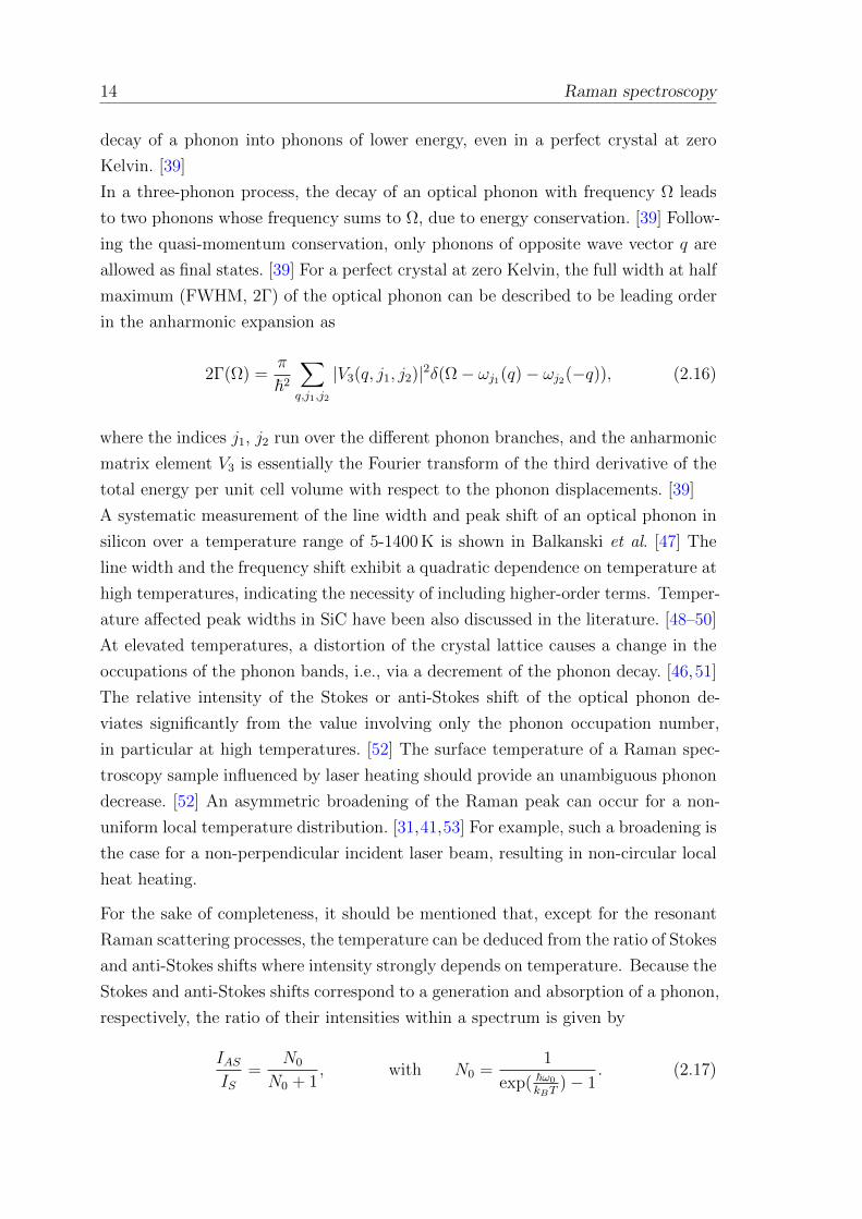
Figure 3.1: Schematic of theconfocal setup. Shown are theprincipal optical components andthe blocking of out-of-focus pho-tons.
comparison to conventional wide field optical mi-
croscopy. The axial focus (focal depth) can be
controlled directly, thus reducing background sig-
nals from outside the confocal volume. A pinhole
in the optical pathway blocks out of focus pho-
tons (Fig. 3.1). The confocal images are gener-
ated by scanning the sample and recording a full
Raman spectrum at each image point. A commer-
cial confocal Raman microscope (alpha 300 R by
WITec; Ulm, Germany; www.witec.de) was used
for all measurements. With a standard 100× ob-
jective (working distance: 0.26 mm; NA = 0.90), a
diffraction-limited focusing of the excitation laser
(Nd:YAG, SHG 532 nm, Pmax = 22.5 mW) is re-
alised. The confocal set up in backscattering ge-
ometry was achieved using the core of a multi-
mode fibre as a pinhole that transmits the light
to the spectrometer. The fibre is mounted in the
image plane of the microscope and can be later-
ally adjusted for maximum collection efficiency. The focal depth can be adjusted by
exchanging the fibre with one of smaller or larger core diameter.
Elastically scattered photons and reflexions were blocked by a sharp edge filter. Full
spectra were acquired on each image point with a lens-based spectrometer with a
back-thinned CCD camera (1024× 128 pixels, cooled to -65 C) with a 19 ms min-
imum integration time. With an 1800 mm−1 grating, the spectral resolution was
1.17 cm−1 per CCD-pixel. Sub-pixel spectral resolution was achieved by fitting a
Lorentz function to the Raman peaks. The samples were scanned with a piezo-
driven scan stage (100× 100× 20µm3) below the objective.
17
18 Methods
3.1.1 Pinhole influence and light suppression
The choice of the pinhole size is crucial because the signal should be intense, implying
a large diameter, but the image resolution should be as high as possible, implying a
smaller diameter.
The response of an imaging system to a point source is given with the point spread
function (PSF). Here, the PSF is mainly determined by the microscope objective.
The effective PSF for the detection is a convolution of the optical PSF (coming
from the optical components) with the detector function of a real two-dimensional
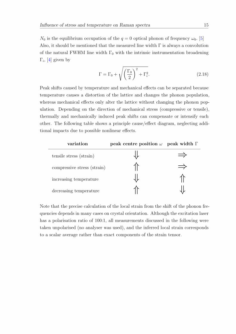
detector with radius vP . Figure 3.2 shows the lateral resolution of a scattering point
vFWHM as a function of detector size vP .
Figure 3.2: Lateral resolution of a scattering point vFWHM as a functionof detector size vP , taken from [54], reproduced with permission.
The size of the pinhole, in optical coordinates, should not exceed vPmax = 2.5 to
avoid a loss of depth resolution. To obtain the highest lateral resolution, the pinhole
size should be below vPmax = 0.5. [54] In practice, the pinhole size can be up to
vPmax = 4 without significantly changing depth resolution and up to vPmax = 2 without
significantly changing lateral resolution. The relationship listed below,
M
NA≥ πd0vPmaxλ
(3.1)
must be satisfied, where M is the magnification, d0 is the pinhole diameter and NA
is the numerical aperture of the objective. Beam path and objective specify the
left side of the equation. The parameter M/NA calculated for several objectives is
shown in the following table (taken with permission from [54]).
The confocal Raman microscope set up 19
objective 10/0.25 20/0.40 40/0.6 60/0.80 100/0.90 100/1.25 100/1.40
M/NA 53 50 67 75 111 80 71
Calculating the right side of equation 3.1 using vPmax = 2.5 and a wavelength of
532 nm, the value is 59 for the fibre with a core diameter of d0 = 25µm, 118 for
50µm and 236 for 100µm. [54] As result, for the 100×, NA = 0.90 objective, the
fibre with the 50µm core diameter has the best compromise between resolution and
light efficiency.
3.1.2 Gaussian laser focusing and beam parameters
When measuring anisotropic samples such as silicon carbide, where the Raman spec-
tra depend on the orientation of the incident laser to the crystal axis, a small amount
of Raman scattering can occur with phonon modes propagating along a different axis
than the chosen one. A non-zero angle between the crystal axis and the incident
photons may occur due to an imperfect alignment of the sample to the laser. This
systematic error can be minimised by careful adjustment. An additional source
of intrinsic error may occur as well: depending on the pinhole diameter, scattered
light may be recorded, which comes from phonon modes propagating in non-chosen
directions.
Laser beams can often be described with a Gaussian function (fundamental or Gaus-
sian modes with TEM00 intensity distributions within the beam profile). Gaussian
beams are usually considered in situations where the beam divergence is relatively
small, so the paraxial approximation can be applied. This approximation allows one
to disregard the term with the second-order derivative in the propagation equation
(as derived from Maxwell’s equations), so that a first-order differential equation re-
sults. For a monochromatic beam propagating in the z direction with the wavelength
λ, the complex electric field amplitude is
E(r, z) = E0w0
w(z)exp
(− r2
w(z)2
)exp
[−i(kz − arctan
z
zR+
kr2
2R(z)
)](3.2)
where |E0| is the peak amplitude, w0 is the smallest beam radius (beam waist),
k = 2π/λ is the wavenumber, ZR is the Rayleigh length, and R(z) is the radius
of curvature of the wavefronts. The oscillating real electric field is obtained by
multiplying the phasor with exp(i2πct/λ) and taking the real part. A plane wave
front of the light can be assumed in the range of the Rayleigh length ZR around
the beam waist w0. The Rayleigh length is defined as the distance from the beam
waist in the propagation direction, where the beam radius is increased by a factor
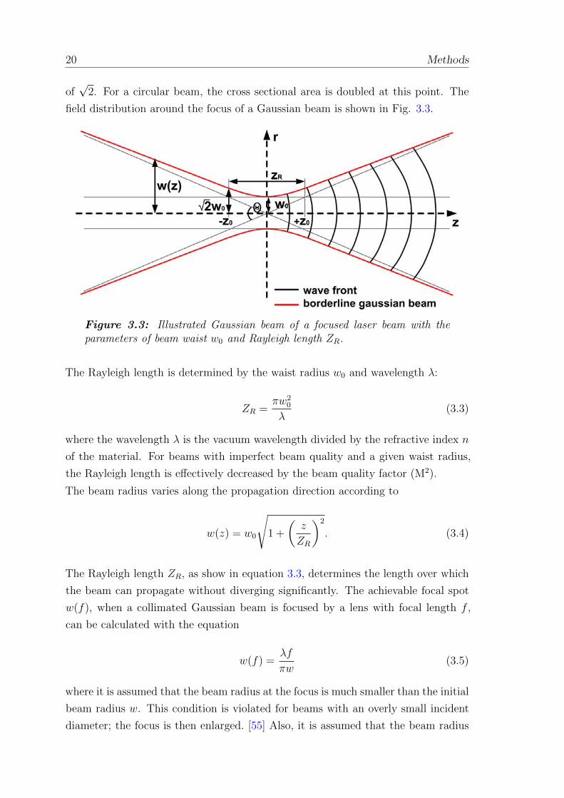
20 Methods
of√
2. For a circular beam, the cross sectional area is doubled at this point. The
field distribution around the focus of a Gaussian beam is shown in Fig. 3.3.
Figure 3.3: Illustrated Gaussian beam of a focused laser beam with theparameters of beam waist w0 and Rayleigh length ZR.
The Rayleigh length is determined by the waist radius w0 and wavelength λ:
ZR =πw2
0
λ(3.3)
where the wavelength λ is the vacuum wavelength divided by the refractive index n
of the material. For beams with imperfect beam quality and a given waist radius,
the Rayleigh length is effectively decreased by the beam quality factor (M2).
The beam radius varies along the propagation direction according to
w(z) = w0
√1 +
(z
ZR
)2
. (3.4)
The Rayleigh length ZR, as show in equation 3.3, determines the length over which
the beam can propagate without diverging significantly. The achievable focal spot
w(f), when a collimated Gaussian beam is focused by a lens with focal length f ,
can be calculated with the equation
w(f) =λf
πw(3.5)
where it is assumed that the beam radius at the focus is much smaller than the initial
beam radius w. This condition is violated for beams with an overly small incident
diameter; the focus is then enlarged. [55] Also, it is assumed that the beam radius
Local heating due to the focused laser beam 21
before focusing is significantly larger than the wavelength λ, so that the paraxial
approximation is valid.
Here, the commonly used fibre with the 50µm core diameter results in a confocal
depth of 1µm. With a Rayleigh length of about 0.5µm when using the (100×,
NA = 0.90) objective, additional peaks arising from other crystal orientations may
be present in the spectra.
3.2 Local heating due to the focused laser beam
Using the 100× objective, the very strong focused laser reaches power densities
of a few MW/cm2 within the focal spot. This high power density may affect the
specimen directly. Heating of silicon by pulsed and continuous wave (cw) lasers was
demonstrated in the 1980s. [56,57]
Light absorbed by the material can lead to an increase in the local temperature
distribution, depending on the thermal conductivity. This results in a local heating
effect, which can be very large at small free-standing structures or at edges. The
energy absorbed in the sample material is
Q(r, t) = I0(1−R) exp
(− r
2
ω20
)(3.6)
where R=R(T,λ) is the reflectivity, I0 is the intensity and ω0 is the radius of the
focused laser. [29]
The recorded Raman scattering originates mostly from the boundary area of the
beam profile, which does not usually correspond to the area of maximal temperature
but to an area of maximal scattering efficiency. [31] Thus, the spectra represent an
average over the whole laser spot.
With increasing local temperature, thermally induced mechanical stress may appear
in the sample. Either an additional line shift due to the locally heated matter (in
the case of silicon and silicon carbide) or, in the case of titanomagnetites, even an
alteration due to heat-induced local oxidation may occur.
3.3 Image generation
Two filtering methods were used for image generation from Raman spectra. Spectra
were measured on each image point, for example in a 100× 100 point matrix. By
integrating the counts in a selected range of wavenumbers around a prominent peak
in each spectrum, compositional images can be created. In a more sophisticated ap-
proach, a Lorentzian peak fit is applied to each spectrum to identify changes in peak
22 Methods
centre and peak width due to, for example, temperature variation or mechanical
stress. By plotting the peak centre, the resulting image represents the stress distri-
bution qualitatively, whereas using the relative variation of the peak width reflects
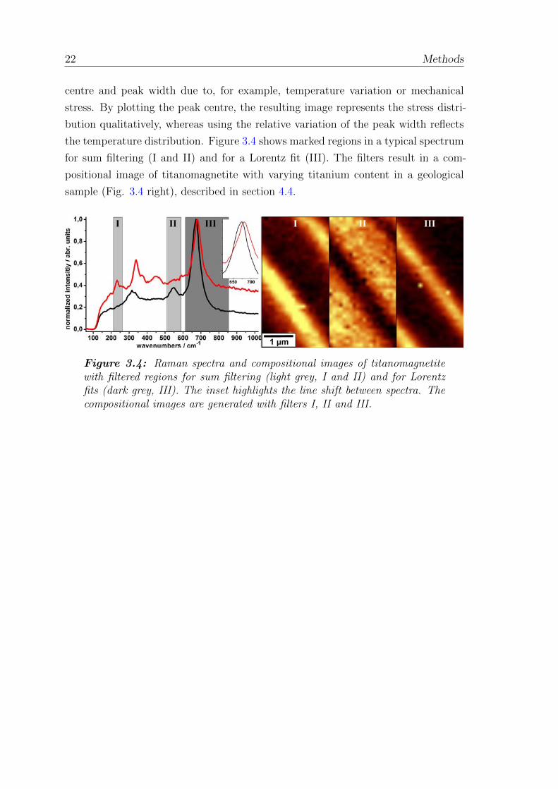
the temperature distribution. Figure 3.4 shows marked regions in a typical spectrum
for sum filtering (I and II) and for a Lorentz fit (III). The filters result in a com-
positional image of titanomagnetite with varying titanium content in a geological
sample (Fig. 3.4 right), described in section 4.4.
Figure 3.4: Raman spectra and compositional images of titanomagnetitewith filtered regions for sum filtering (light grey, I and II) and for Lorentzfits (dark grey, III). The inset highlights the line shift between spectra. Thecompositional images are generated with filters I, II and III.
4 Spectroscopic characterisation
4.1 Silicon
Silicon is by far the most used and best investigated of the semiconductor materials.
It has the same diamond cubic crystal structure as diamond, with each silicon atom
covalently bonded in between four neighbours. Positively or negatively doped silicon
(p- and n-type silicon) is used in electronic devices such as transistors for integrated
circuits (ICs), flash memory and microprocessors. Because the properties and man-
ufacturing methods of silicon are well known, silicon is used not only in electronic
circuits but also in micro-electro-mechanical systems (MEMS) for sensor technology
applications as a cheap and easy-to-use substrate material.
Raman spectroscopy can provide information about stress and local temperatures
in a device during operation and residual stress after fabrication. These parameters
are important to optimise manufacturing and increase reliability of the device.
4.1.1 Phonon dispersion curve and band structure
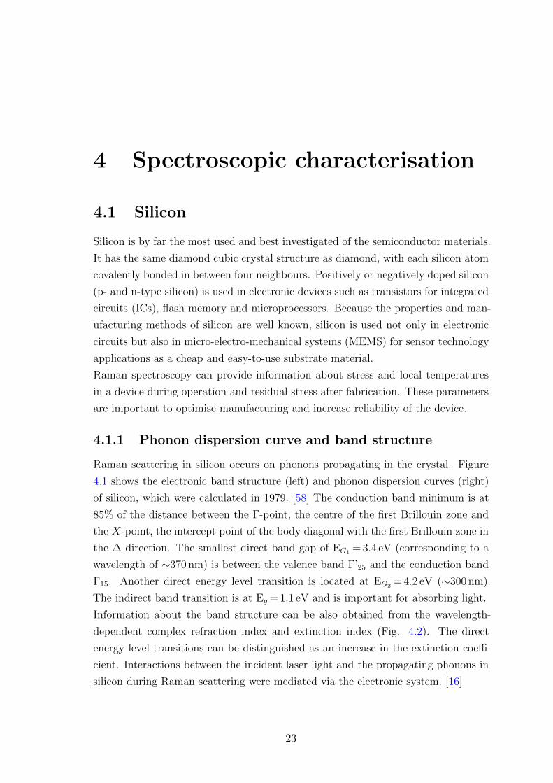
Raman scattering in silicon occurs on phonons propagating in the crystal. Figure
4.1 shows the electronic band structure (left) and phonon dispersion curves (right)
of silicon, which were calculated in 1979. [58] The conduction band minimum is at
85% of the distance between the Γ-point, the centre of the first Brillouin zone and
the X-point, the intercept point of the body diagonal with the first Brillouin zone in
the ∆ direction. The smallest direct band gap of EG1 = 3.4 eV (corresponding to a
wavelength of ∼370 nm) is between the valence band Γ’25 and the conduction band
Γ15. Another direct energy level transition is located at EG2 = 4.2 eV (∼300 nm).
The indirect band transition is at Eg = 1.1 eV and is important for absorbing light.
Information about the band structure can be also obtained from the wavelength-
dependent complex refraction index and extinction index (Fig. 4.2). The direct
energy level transitions can be distinguished as an increase in the extinction coeffi-
cient. Interactions between the incident laser light and the propagating phonons in
silicon during Raman scattering were mediated via the electronic system. [16]
23
24 Spectroscopic characterisation
Figure 4.1: Electronic band structure (left). The unoccupied areas are ingrey. Phonon dispersion curves (right) of silicon. The red circle indicates theΓ-point of the phonons on which scattering occurs, taken from [59] and [16],reproduced with permission.
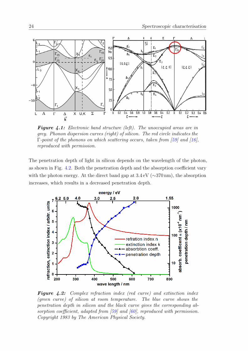
The penetration depth of light in silicon depends on the wavelength of the photon,
as shown in Fig. 4.2. Both the penetration depth and the absorption coefficient vary
with the photon energy. At the direct band gap at 3.4 eV (∼370 nm), the absorption
increases, which results in a decreased penetration depth.
Figure 4.2: Complex refraction index (red curve) and extinction index(green curve) of silicon at room temperature. The blue curve shows thepenetration depth in silicon and the black curve gives the corresponding ab-sorption coefficient, adapted from [59] and [60], reproduced with permission.Copyright 1983 by The American Physical Society.
Silicon 25
The penetration depth and absorption coefficient determine the local heating of the
material under the focused laser. For near-surface investigations, the scattering re-
gion can be limited to the area of interest by choosing an adequate laser wavelength.
4.1.2 Raman scattering in silicon
Because of the cubic symmetry of silicon, the optical phonon branches are triply
degenerate at the Γ-point, corresponding to about 521 cm−1 at room temperature
with F2g symmetry (marked with a red circle in Fig. 4.1), regarding the conversion
factors of
8.0655 cm−1 , 1 meV , 0.2418 THz (4.1)
where the Γ-point is at 15.5 THz. [16] The triple degeneracy of the silicon phonon
can be lifted by mechanical stress. [1, 28]
Three Raman tensors exist for silicon, given as x = [100], y = [010] and z = [001] in
the crystal coordinate system (see Eq. 2.8). A phonon can be considered longitudinal
or transversal depending on the surface from which the scattering is observed. Rx
and Ry correspond to the transverse optical phonons (TO) polarised along x and
y. Rz corresponds to the longitudinal optical phonon (LO) polarised along z in
(001) backscattering, whereas Rx corresponds to the LO phonon for (100) back
scattering. [3,16] This influence of crystallographic orientation on the Raman spectra
was investigated by means of polarisation measurements. [61]
The following table gives the polarisation selection rules for backscattering from
a (001) and (110) silicon surface as indicated in equation 2.8 and 2.9, taken with
permission from [3].
Polarization Visibleei es Rx Ry Rz
Backscattering from (001)(100) (100) - - -(100) (010) - - ×(1-10) (1-10) - - ×(110) (1-10) - - -
Backscattering from (110) - - ×(1-10) (001) × × -(1-10) (1-10) - - ×(001) (001) - - -
Only two polarisation configurations permit Raman scattering for (001) back-
scattering: [3, 16]
26 Spectroscopic characterisation
1. ei and es are perpendicular: z(x,y)-z with x parallel to (100)
2. ei and es are parallel: z(x,x)-z with x parallel to (110).
In both cases, only the LO phonons can be observed. To observe the TO phonons,
a different scattering geometry, such as 90 scattering, or backscattering from (110),
would be needed.
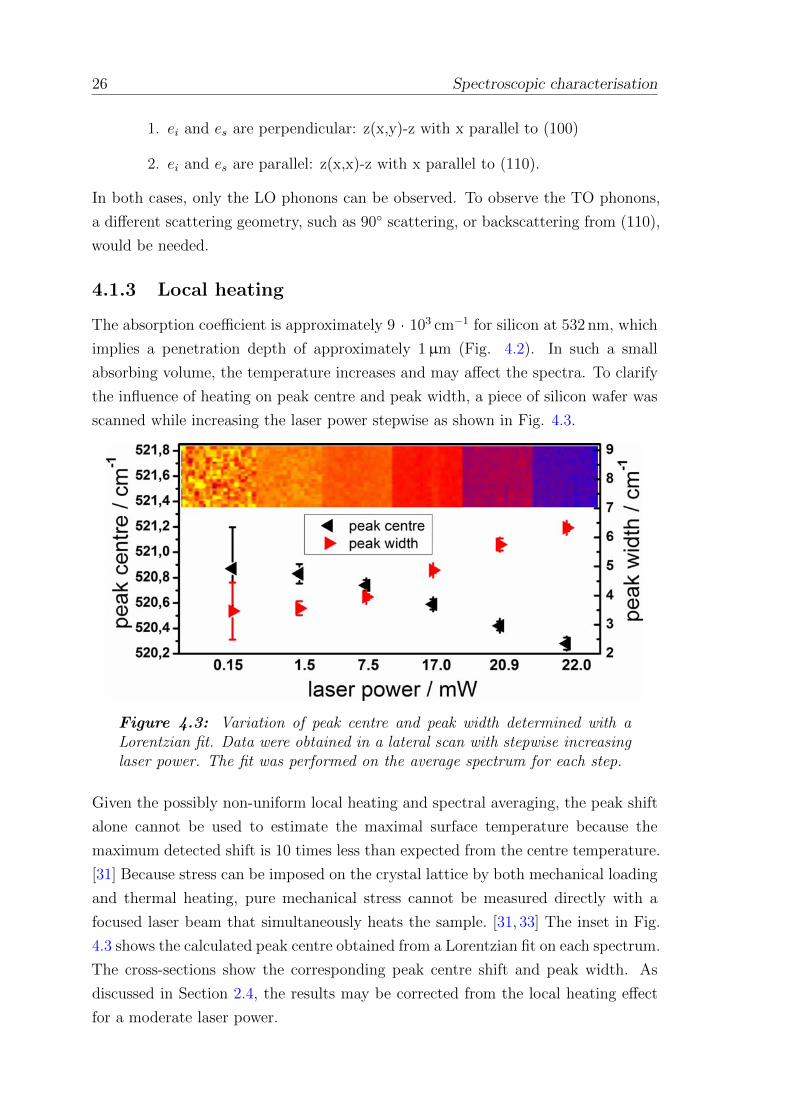
4.1.3 Local heating
The absorption coefficient is approximately 9 · 103 cm−1 for silicon at 532 nm, which
implies a penetration depth of approximately 1µm (Fig. 4.2). In such a small
absorbing volume, the temperature increases and may affect the spectra. To clarify
the influence of heating on peak centre and peak width, a piece of silicon wafer was
scanned while increasing the laser power stepwise as shown in Fig. 4.3.
Figure 4.3: Variation of peak centre and peak width determined with aLorentzian fit. Data were obtained in a lateral scan with stepwise increasinglaser power. The fit was performed on the average spectrum for each step.
Given the possibly non-uniform local heating and spectral averaging, the peak shift
alone cannot be used to estimate the maximal surface temperature because the
maximum detected shift is 10 times less than expected from the centre temperature.
[31] Because stress can be imposed on the crystal lattice by both mechanical loading
and thermal heating, pure mechanical stress cannot be measured directly with a
focused laser beam that simultaneously heats the sample. [31, 33] The inset in Fig.
4.3 shows the calculated peak centre obtained from a Lorentzian fit on each spectrum.
The cross-sections show the corresponding peak centre shift and peak width. As
discussed in Section 2.4, the results may be corrected from the local heating effect
for a moderate laser power.
Silicon carbide 27
4.1.4 Experimental results
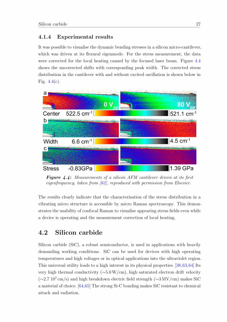
It was possible to visualise the dynamic bending stresses in a silicon micro-cantilever,
which was driven at its flexural eigenmode. For the stress measurement, the data
were corrected for the local heating caused by the focused laser beam. Figure 4.4
shows the uncorrected shifts with corresponding peak width. The corrected stress
distribution in the cantilever with and without excited oscillation is shown below in
Fig. 4.4(c).
Figure 4.4: Measurements of a silicon AFM cantilever driven at its firsteigenfrequency, taken from [62], reproduced with permission from Elsevier.
The results clearly indicate that the characterisation of the stress distribution in a
vibrating micro structure is accessible by micro Raman spectroscopy. This demon-
strates the usability of confocal Raman to visualise appearing stress fields even while
a device is operating and the measurement correction of local heating.
4.2 Silicon carbide
Silicon carbide (SiC), a robust semiconductor, is used in applications with heavily
demanding working conditions. SiC can be used for devices with high operating
temperatures and high voltages or in optical applications into the ultraviolet region.
This universal utility leads to a high interest in its physical properties. [38,63,64] Its
very high thermal conductivity (∼5.0 W/cm), high saturated electron drift velocity
(∼2.7 107 cm/s) and high breakdown electric field strength (∼3 MV/cm) makes SiC
a material of choice. [64,65] The strong Si-C bonding makes SiC resistant to chemical
attack and radiation.
28 Spectroscopic characterisation
For example, SiC is used in insulated-gate bipolar transistors as a semiconductor for
pulsed power applications, switching several megawatts of electrical power in several
nanoseconds. [64] As a sensor material, SiC is able to work reliably in conditions
where other materials may malfunction. These electronic devices will offer more
efficient and cheaper systems and open a new generation of electronic equipment
not requiring cooling and transformers. As with silicon, Raman spectroscopy can
provide information for improved manufacturing parameters giving reduced residual
stress or optimisation of the device during operation.
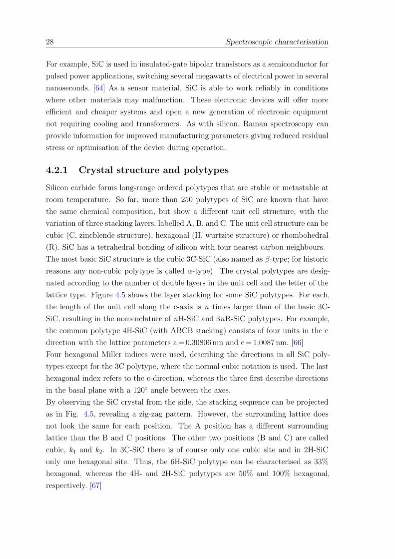
4.2.1 Crystal structure and polytypes
Silicon carbide forms long-range ordered polytypes that are stable or metastable at
room temperature. So far, more than 250 polytypes of SiC are known that have
the same chemical composition, but show a different unit cell structure, with the
variation of three stacking layers, labelled A, B, and C. The unit cell structure can be
cubic (C, zincblende structure), hexagonal (H, wurtzite structure) or rhombohedral
(R). SiC has a tetrahedral bonding of silicon with four nearest carbon neighbours.
The most basic SiC structure is the cubic 3C-SiC (also named as β-type; for historic
reasons any non-cubic polytype is called α-type). The crystal polytypes are desig-
nated according to the number of double layers in the unit cell and the letter of the
lattice type. Figure 4.5 shows the layer stacking for some SiC polytypes. For each,
the length of the unit cell along the c-axis is n times larger than of the basic 3C-
SiC, resulting in the nomenclature of nH-SiC and 3nR-SiC polytypes. For example,
the common polytype 4H-SiC (with ABCB stacking) consists of four units in the c
direction with the lattice parameters a = 0.30806 nm and c = 1.0087 nm. [66]
Four hexagonal Miller indices were used, describing the directions in all SiC poly-
types except for the 3C polytype, where the normal cubic notation is used. The last
hexagonal index refers to the c-direction, whereas the three first describe directions
in the basal plane with a 120 angle between the axes.
By observing the SiC crystal from the side, the stacking sequence can be projected
as in Fig. 4.5, revealing a zig-zag pattern. However, the surrounding lattice does
not look the same for each position. The A position has a different surrounding
lattice than the B and C positions. The other two positions (B and C) are called
cubic, k1 and k2. In 3C-SiC there is of course only one cubic site and in 2H-SiC
only one hexagonal site. Thus, the 6H-SiC polytype can be characterised as 33%
hexagonal, whereas the 4H- and 2H-SiC polytypes are 50% and 100% hexagonal,
respectively. [67]
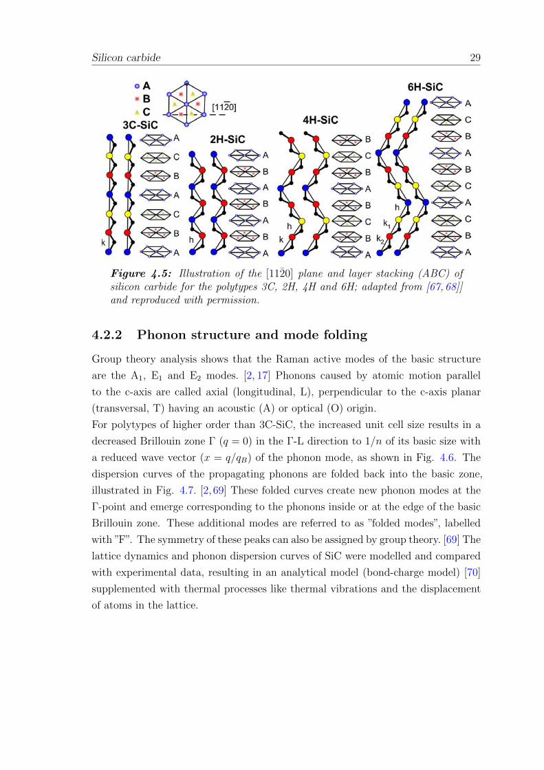
Silicon carbide 29
Figure 4.5: Illustration of the [1120] plane and layer stacking (ABC) ofsilicon carbide for the polytypes 3C, 2H, 4H and 6H; adapted from [67, 68]]and reproduced with permission.
4.2.2 Phonon structure and mode folding
Group theory analysis shows that the Raman active modes of the basic structure
are the A1, E1 and E2 modes. [2, 17] Phonons caused by atomic motion parallel
to the c-axis are called axial (longitudinal, L), perpendicular to the c-axis planar
(transversal, T) having an acoustic (A) or optical (O) origin.
For polytypes of higher order than 3C-SiC, the increased unit cell size results in a
decreased Brillouin zone Γ (q = 0) in the Γ-L direction to 1/n of its basic size with
a reduced wave vector (x = q/qB) of the phonon mode, as shown in Fig. 4.6. The
dispersion curves of the propagating phonons are folded back into the basic zone,
illustrated in Fig. 4.7. [2, 69] These folded curves create new phonon modes at the
Γ-point and emerge corresponding to the phonons inside or at the edge of the basic
Brillouin zone. These additional modes are referred to as ”folded modes”, labelled
with ”F”. The symmetry of these peaks can also be assigned by group theory. [69] The
lattice dynamics and phonon dispersion curves of SiC were modelled and compared
with experimental data, resulting in an analytical model (bond-charge model) [70]
supplemented with thermal processes like thermal vibrations and the displacement
of atoms in the lattice.
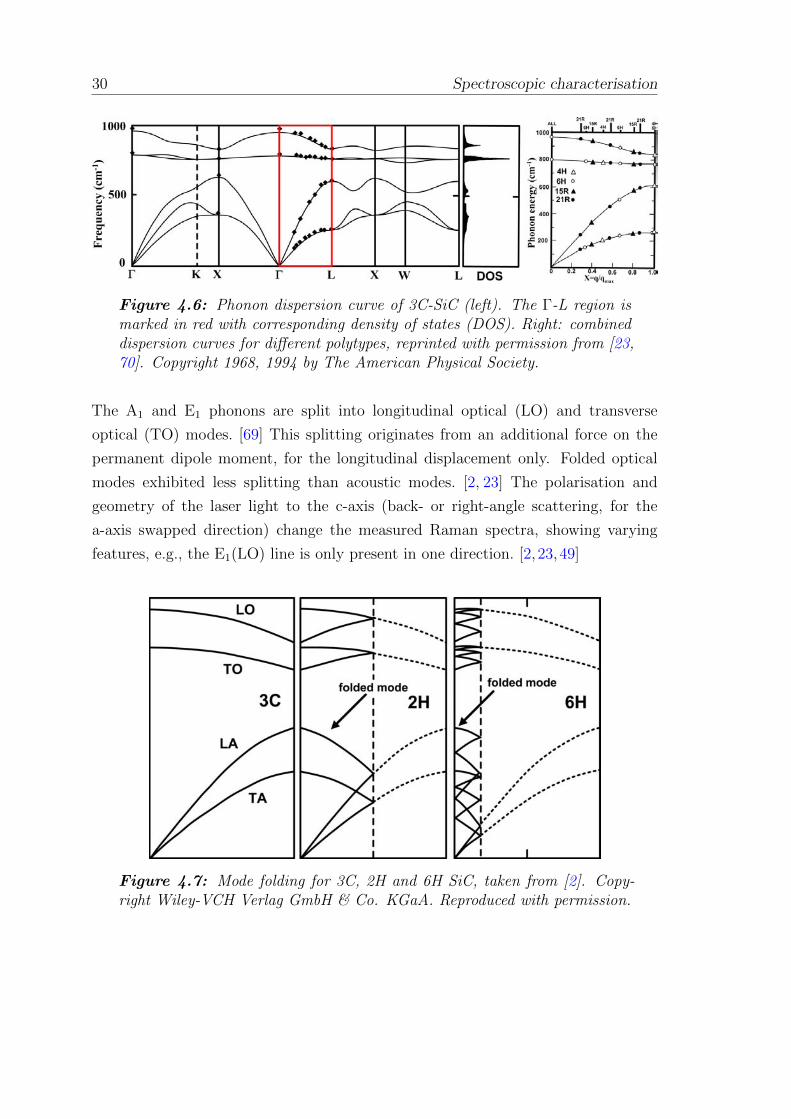
30 Spectroscopic characterisation
Figure 4.6: Phonon dispersion curve of 3C-SiC (left). The Γ-L region ismarked in red with corresponding density of states (DOS). Right: combineddispersion curves for different polytypes, reprinted with permission from [23,70]. Copyright 1968, 1994 by The American Physical Society.
The A1 and E1 phonons are split into longitudinal optical (LO) and transverse
optical (TO) modes. [69] This splitting originates from an additional force on the
permanent dipole moment, for the longitudinal displacement only. Folded optical
modes exhibited less splitting than acoustic modes. [2, 23] The polarisation and
geometry of the laser light to the c-axis (back- or right-angle scattering, for the
a-axis swapped direction) change the measured Raman spectra, showing varying
features, e.g., the E1(LO) line is only present in one direction. [2, 23,49]
Figure 4.7: Mode folding for 3C, 2H and 6H SiC, taken from [2]. Copy-right Wiley-VCH Verlag GmbH & Co. KGaA. Reproduced with permission.
Silicon carbide 31
4.2.3 Raman line shift
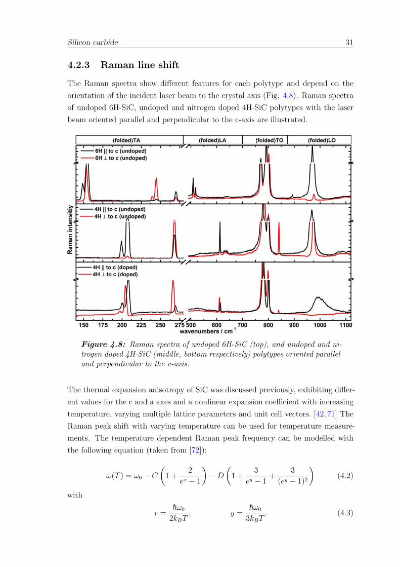
The Raman spectra show different features for each polytype and depend on the
orientation of the incident laser beam to the crystal axis (Fig. 4.8). Raman spectra
of undoped 6H-SiC, undoped and nitrogen doped 4H-SiC polytypes with the laser
beam oriented parallel and perpendicular to the c-axis are illustrated.
Figure 4.8: Raman spectra of undoped 6H-SiC (top), and undoped and ni-trogen doped 4H-SiC (middle, bottom respectively) polytypes oriented paralleland perpendicular to the c-axis.
The thermal expansion anisotropy of SiC was discussed previously, exhibiting differ-
ent values for the c and a axes and a nonlinear expansion coefficient with increasing
temperature, varying multiple lattice parameters and unit cell vectors. [42, 71] The
Raman peak shift with varying temperature can be used for temperature measure-
ments. The temperature dependent Raman peak frequency can be modelled with
the following equation (taken from [72]):
ω(T ) = ω0 − C(
1 +2
ex − 1
)−D
(1 +
3
ey − 1+
3
(ey − 1)2
)(4.2)
with
x =~ω0
2kBT, y =
~ω0
3kBT. (4.3)
32 Spectroscopic characterisation
The constants C and D are fitting parameters. In ~ω0, the anharmonic interaction is
neglected, and kBT is the thermal energy. The term starting with D can be neglected
for moderate temperatures (less than 500 C), resulting in a linear dependency of
frequency on temperature. For temperatures up to 1000 C, four anharmonic terms
must be considered in the Hamiltonian model and an additional peak shift must
be taken in account, as well stresses inside the bulk material. [33] The shift of the
E2(FTO) Raman peak of undoped 6H-SiC with increasing temperature was used for
temperature measurements inside a light emitting diode made from SiC. [72]
The dependence of the Raman spectra of SiC on isotropic pressure has been inves-
tigated experimentally and theoretically. [35, 36, 40, 42, 66, 71, 73] It is possible with
ab initio and group theory methods to calculate this dependence. [69,70,74]
With nitrogen doping as an electron donor, the spectral shape and width as well as
the peak position of the A1 phonon (LO) vary with concentration. This effect can
be assigned to a plasmon-phonon coupling. [69,74] The plasmon-coupled LO phonon
(LOPC) was used to characterise ion-implanted SiC for different annealing temper-
atures. [75] Harima et al. investigated the plasmon frequency, carrier and phonon
damping deduced from line shape by means of Raman scattering from anisotropic
LO phonon plasmon coupling in n-type 4H- and 6H-SiC. [49] Owing to the major
effect of the LO damping, the LOPC line shape can be used to obtain the carrier
density and mobility. [49] Previous experimental and theoretical studies describe the
isotropic pressure dependence shift of the Raman lines in SiC. Carrier mobility and
concentration deduced from Raman spectroscopy show a reasonable agreement with
those found by electrical measurements. [49]
4.2.4 Local heating
In contrast to silicon, the local heating effect in silicon carbide can be neglected
due to the minimal influence of the laser. The change in peak centre position is in
the same range for the investigated polytypes 6H-SiC (LO peak, 0.005 cm−1/mW)
and 4H-SiC (LO peak, 0.006 cm−1/mW). For comparison, the shift in silicon is
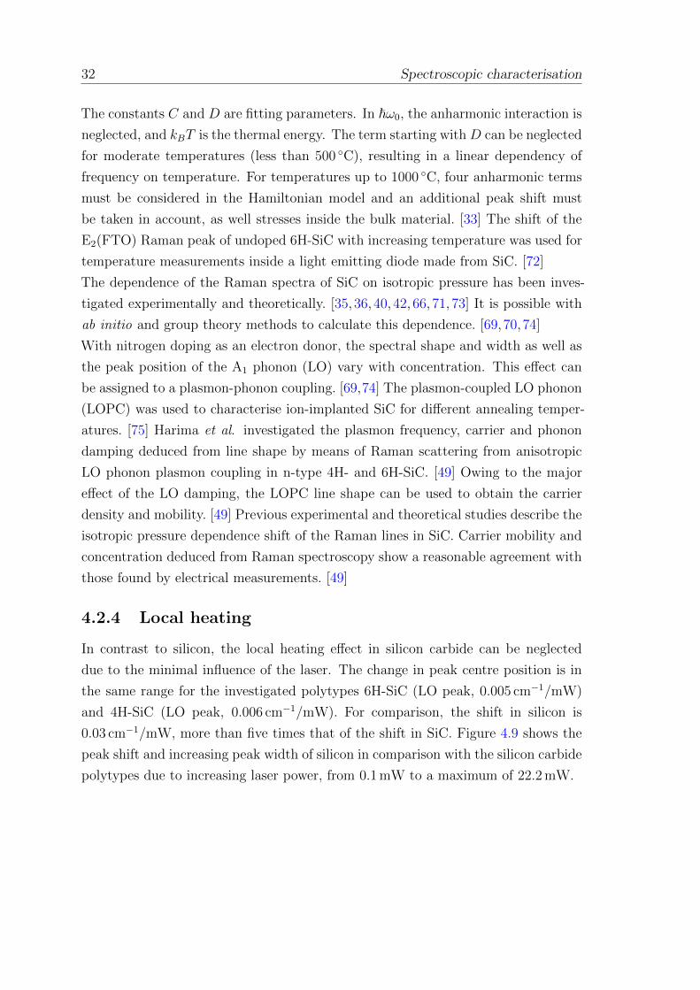
0.03 cm−1/mW, more than five times that of the shift in SiC. Figure 4.9 shows the
peak shift and increasing peak width of silicon in comparison with the silicon carbide
polytypes due to increasing laser power, from 0.1 mW to a maximum of 22.2 mW.
Silicon carbide 33
Figure 4.9: Temperature-induced peak shift and increasing peak width ofsilicon in comparison to SiC polytypes. The influence of local laser heatingfor SiC is much smaller than for silicon.
4.2.5 Experimental results
The peak positions of the Raman lines in silicon carbide vary linearly with temper-
ature. The slope of the temperature shift increases with increased energy transfer
due to inelastic scattering, showing a linear dependence with temperature in the
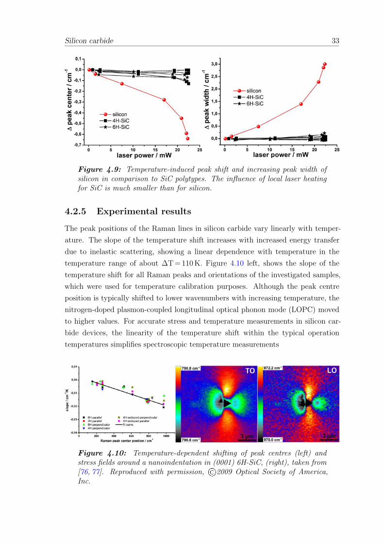
temperature range of about ∆T = 110 K. Figure 4.10 left, shows the slope of the
temperature shift for all Raman peaks and orientations of the investigated samples,
which were used for temperature calibration purposes. Although the peak centre
position is typically shifted to lower wavenumbers with increasing temperature, the
nitrogen-doped plasmon-coupled longitudinal optical phonon mode (LOPC) moved
to higher values. For accurate stress and temperature measurements in silicon car-
bide devices, the linearity of the temperature shift within the typical operation
temperatures simplifies spectroscopic temperature measurements
Figure 4.10: Temperature-dependent shifting of peak centres (left) andstress fields around a nanoindentation in (0001) 6H-SiC, (right), taken from[76, 77]. Reproduced with permission, ©2009 Optical Society of America,Inc.
34 Spectroscopic characterisation
The stress fields in silicon carbide caused by nanoindentations show the stress dis-
tribution in the material (Fig. 4.10, right). A comparison with s-SNOM (scattering
scanning near-field optical microscope) measurements reveal a similar qualitative
contrast of the strain fields around nanoindentation sites, corresponding in their
spatial distribution and their qualitative sign (compressive/tensile). The Raman
frequency shifts can be directly related to local strain, in much the same way as was
observed with s-SNOM. The magnitude of the phonon line shift agrees well with
the shift of the phonon-polariton near-field resonance. Thus, s-SNOM allows for
the resolution of the smallest features of the indent down to nanocracks, whereas
diffraction limited confocal Raman spectroscopy gives full spectral information for
the changes in phonon dispersion. Scattering-SNOM is sensitive to the strain distri-
bution near the surface, whereas far-field Raman scattering also occurs beneath the
surface and can reveal changes in sub-surface strain distributions.
4.3 Alteration of calcium fluoride caused by UV-
light
Intense ultraviolet laser radiation may cause surface damage in optical components.
[78] Depending on the substrate material and coatings, optical components in a laser
will start to degrade at a certain power level. [6, 79–84] The damage first appears
at the exterior surface before intracavity damage occurs. The effect is proportional
to the square of the field and disappears if there is a perfect antireflection coating
on the surface, as first mentioned by Boling in 1973. [6] Working with deep UV
light (DUV) limits the number of substrate materials that are transmissive in this
spectral range. The most common UV lasers are excimer lasers, which are very
intense ultraviolet light sources, generating laser pulses in the nanosecond range
with high power densities. Common lasers are krypton fluoride (KrF, 248 nm) and
argon fluoride (ArF, 193 nm), used for optical lithography, medical and industrial
applications and in metrology. The active media are the so-called excimer (excited
dimer) molecules, which represent a bound state of their noble gas and halogen
constituents only in the excited electronic state, but not in the ground state.
The preferred material for excimer laser optical components is metal-fluoride crystals,
due to their excellent optical properties, large band gap energies and resistance to
the fluorine-containing laser gas. High reflective and outcoupling resonator mirrors
are usually dielectric mirrors. The reflective coatings are made of an alternating
sequence of λ/4 metal-fluoride layers with high and low refractive indices, commonly
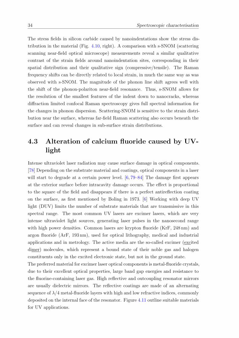
deposited on the internal face of the resonator. Figure 4.11 outline suitable materials
for UV applications.
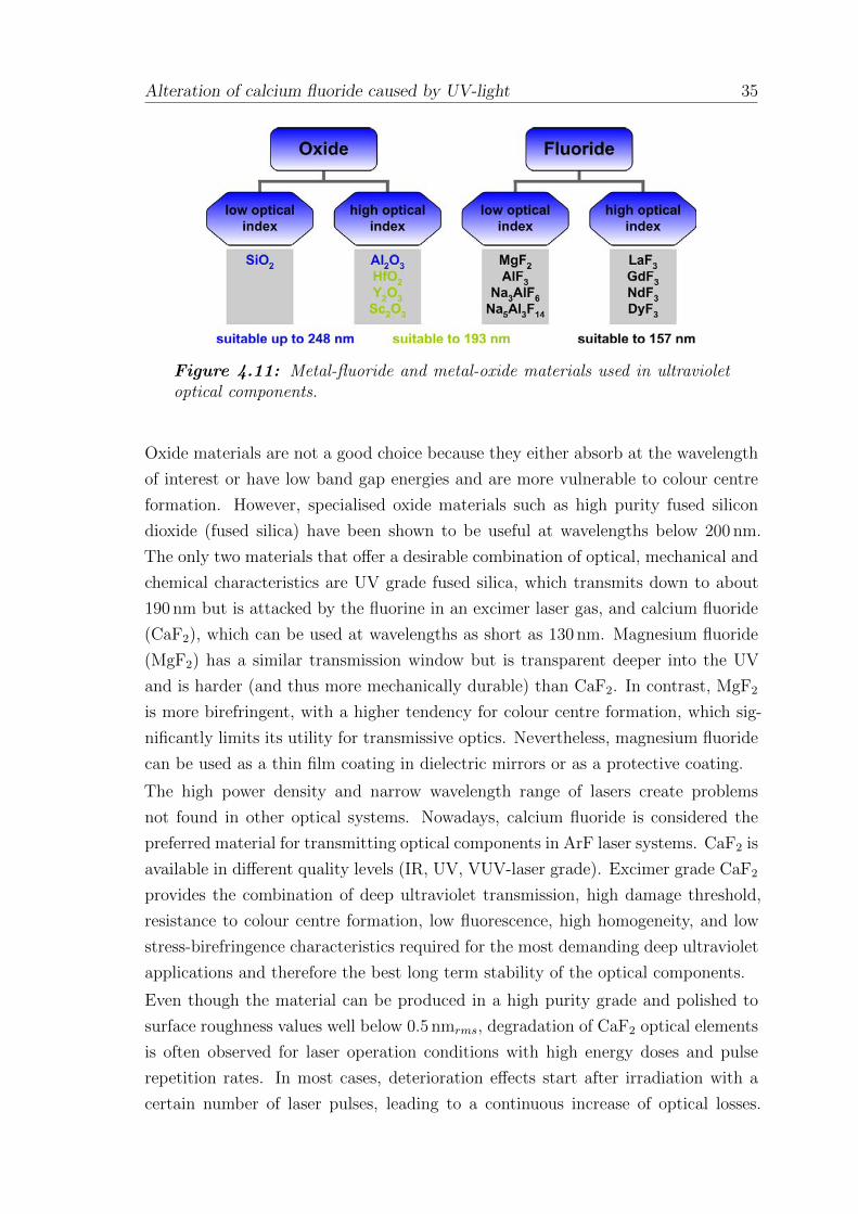
Alteration of calcium fluoride caused by UV-light 35
Figure 4.11: Metal-fluoride and metal-oxide materials used in ultravioletoptical components.
Oxide materials are not a good choice because they either absorb at the wavelength
of interest or have low band gap energies and are more vulnerable to colour centre
formation. However, specialised oxide materials such as high purity fused silicon
dioxide (fused silica) have been shown to be useful at wavelengths below 200 nm.
The only two materials that offer a desirable combination of optical, mechanical and
chemical characteristics are UV grade fused silica, which transmits down to about
190 nm but is attacked by the fluorine in an excimer laser gas, and calcium fluoride
(CaF2), which can be used at wavelengths as short as 130 nm. Magnesium fluoride
(MgF2) has a similar transmission window but is transparent deeper into the UV
and is harder (and thus more mechanically durable) than CaF2. In contrast, MgF2
is more birefringent, with a higher tendency for colour centre formation, which sig-
nificantly limits its utility for transmissive optics. Nevertheless, magnesium fluoride
can be used as a thin film coating in dielectric mirrors or as a protective coating.
The high power density and narrow wavelength range of lasers create problems
not found in other optical systems. Nowadays, calcium fluoride is considered the
preferred material for transmitting optical components in ArF laser systems. CaF2 is
available in different quality levels (IR, UV, VUV-laser grade). Excimer grade CaF2
provides the combination of deep ultraviolet transmission, high damage threshold,
resistance to colour centre formation, low fluorescence, high homogeneity, and low
stress-birefringence characteristics required for the most demanding deep ultraviolet
applications and therefore the best long term stability of the optical components.
Even though the material can be produced in a high purity grade and polished to
surface roughness values well below 0.5 nmrms, degradation of CaF2 optical elements
is often observed for laser operation conditions with high energy doses and pulse
repetition rates. In most cases, deterioration effects start after irradiation with a
certain number of laser pulses, leading to a continuous increase of optical losses.
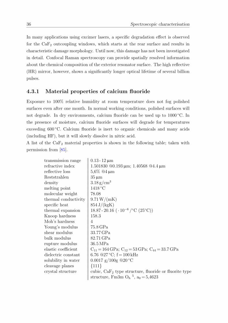
36 Spectroscopic characterisation
In many applications using excimer lasers, a specific degradation effect is observed
for the CaF2 outcoupling windows, which starts at the rear surface and results in
characteristic damage morphology. Until now, this damage has not been investigated
in detail. Confocal Raman spectroscopy can provide spatially resolved information
about the chemical composition of the exterior resonator surface. The high reflective
(HR) mirror, however, shows a significantly longer optical lifetime of several billion
pulses.
4.3.1 Material properties of calcium fluoride
Exposure to 100% relative humidity at room temperature does not fog polished
surfaces even after one month. In normal working conditions, polished surfaces will
not degrade. In dry environments, calcium fluoride can be used up to 1000 C. In
the presence of moisture, calcium fluoride surfaces will degrade for temperatures
exceeding 600 C. Calcium fluoride is inert to organic chemicals and many acids
(including HF), but it will slowly dissolve in nitric acid.
A list of the CaF2 material properties is shown in the following table; taken with
permission from [85].
transmission range 0.13 - 12µmrefractive index 1.501830 @0.193µm; 1.40568 @4.4µmreflective loss 5,6% @4µmReststrahlen 35µmdensity 3.18 g/cm3
melting point 1418 Cmolecular weight 78.08thermal conductivity 9.71 W/(mK)specific heat 854 J/(kgK)thermal expansion 18.87 - 20.16 ( · 10−6 /C (25C))Knoop hardness 158.3Moh’s hardness 4Young’s modulus 75.8 GPashear modulus 33.77 GPabulk modulus 82.71 GParupture modulus 36.5 MPaelastic coefficient C11 = 164 GPa; C12 = 53 GPa; C44 = 33.7 GPadielectric constant 6.76 @27 C; f = 100 kHzsolubility in water 0.0017 g/100g @20 Ccleavage planes 111crystal structure cubic, CaF2 type structure, fluoride or fluorite type
structure, Fm3m Oh5, a0 = 5,4623
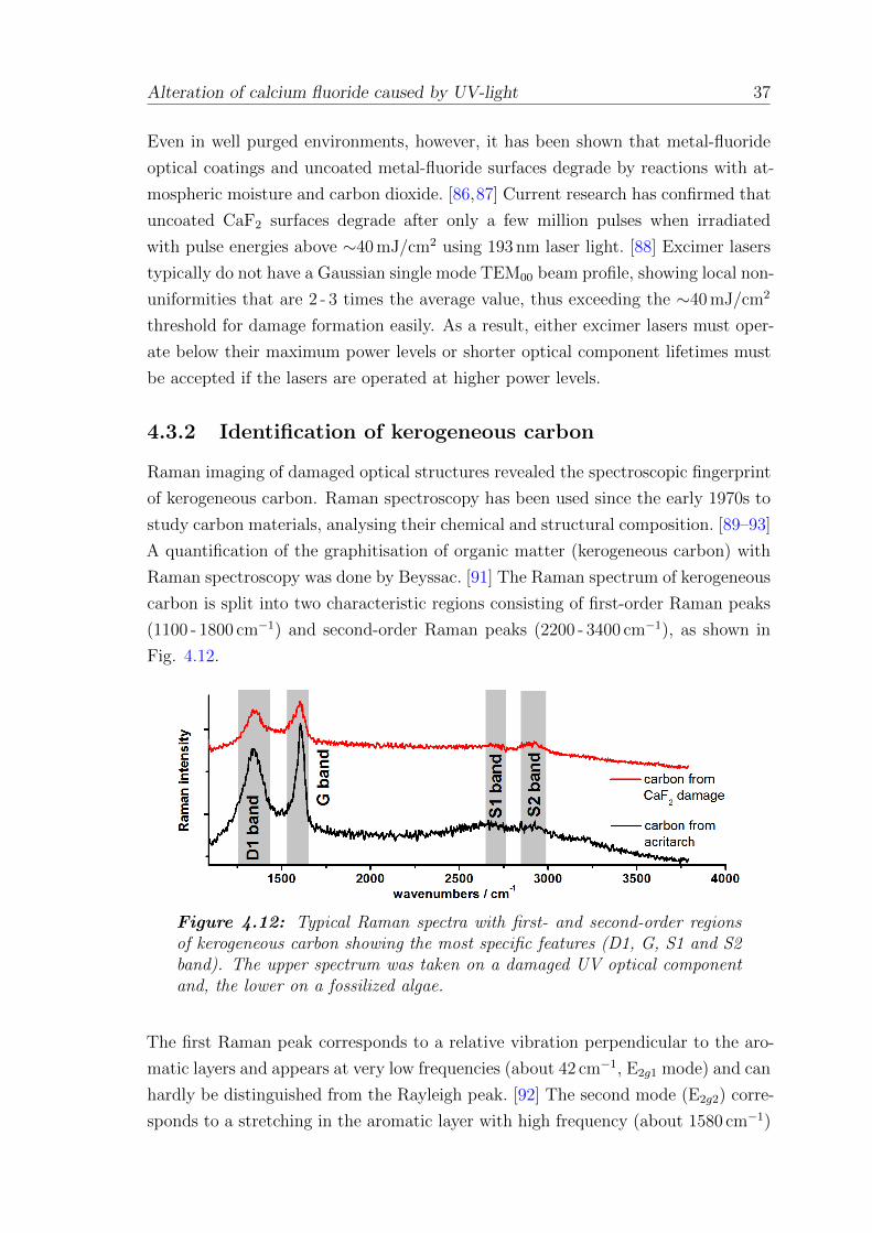
Alteration of calcium fluoride caused by UV-light 37
Even in well purged environments, however, it has been shown that metal-fluoride
optical coatings and uncoated metal-fluoride surfaces degrade by reactions with at-
mospheric moisture and carbon dioxide. [86,87] Current research has confirmed that
uncoated CaF2 surfaces degrade after only a few million pulses when irradiated
with pulse energies above ∼40 mJ/cm2 using 193 nm laser light. [88] Excimer lasers
typically do not have a Gaussian single mode TEM00 beam profile, showing local non-
uniformities that are 2 - 3 times the average value, thus exceeding the ∼40 mJ/cm2
threshold for damage formation easily. As a result, either excimer lasers must oper-
ate below their maximum power levels or shorter optical component lifetimes must
be accepted if the lasers are operated at higher power levels.
4.3.2 Identification of kerogeneous carbon
Raman imaging of damaged optical structures revealed the spectroscopic fingerprint
of kerogeneous carbon. Raman spectroscopy has been used since the early 1970s to
study carbon materials, analysing their chemical and structural composition. [89–93]
A quantification of the graphitisation of organic matter (kerogeneous carbon) with
Raman spectroscopy was done by Beyssac. [91] The Raman spectrum of kerogeneous
carbon is split into two characteristic regions consisting of first-order Raman peaks
(1100 - 1800 cm−1) and second-order Raman peaks (2200 - 3400 cm−1), as shown in
Fig. 4.12.
Figure 4.12: Typical Raman spectra with first- and second-order regionsof kerogeneous carbon showing the most specific features (D1, G, S1 and S2band). The upper spectrum was taken on a damaged UV optical componentand, the lower on a fossilized algae.
The first Raman peak corresponds to a relative vibration perpendicular to the aro-
matic layers and appears at very low frequencies (about 42 cm−1, E2g1 mode) and can
hardly be distinguished from the Rayleigh peak. [92] The second mode (E2g2) corre-
sponds to a stretching in the aromatic layer with high frequency (about 1580 cm−1)
38 Spectroscopic characterisation
normally labelled the G-band. [92] In perfect crystals such as graphite, only the G-
band will appear in the first order region. For poorly organised carbon, additional
bands appear around 1150 cm−1, 1350 cm−1 (D1 band and a defect band with A1g
symmetry from in-plane defects and heteroatoms, [94]), 1500 cm−1 (D3 band) and
1620 cm−1 (D2 band). [92] The most important features are the D1 and G bands,
with the D2 and D3 band appearing as shoulders in the G band. The D2 and D1
bands are always present together and their intensities decrease with an increasing
degree of organisation. The peaks in the second-order region come from overtones or
combination scattering appearing near 2400 cm−1, 2700 cm−1 (S1 band), 2900 cm−1
(S2 band) and 3300 cm−1. [90, 92]
The degree of organization can be determined by the peak position, peak width
and the D1/G intensity ratio (R1 ratio) with the D1/(G+D1+D2) area ratio (R2
ratio) used for describing the carbonisation process. [90–92] Present temperatures
and pressure levels can be derived by analysing the R1 and R2 ratios of the kerogen
Raman spectra.
4.3.3 Experimental results
UV irradiation with high energy densities of 80 mJ/cm2 and 193 nm wavelength
causes surface damage within several hundred million pulses. Portions of the mirror’s
exterior surface are altered from the CaF2 bulk material into CaCO3 (calcite). The
surface roughens and increases scattering losses in addition to the absorption losses
of the altered material. The deterioration is driven by temperature and the photo-
induced chemistry caused by the UV laser light. The alteration starts at the edge
of the beam profile where the highest temperature gradients occur. The CaCO3
crystals, which are a few micrometers in size, are embedded in a variety of organic
material. Highly energetic photons induce photochemical reactions of imperfections
located at the interface between the substrate and coating or with contaminants from
the environment. Figure 4.13 shows the surface damage of a mirror irradiated with
250 million pulses (a) and (d) and 100 million pulses (b), (c) and (e), respectively.
The lateral scan in Fig. 4.13(a) outlines the CaF2 intensity, and (d) shows the
CaCO3 intensity in yellow and organics in bright blue at the same position. Figure
4.13(b) illustrate CaCO3 in red and organic matter in green, and (c) kerogeneous
carbon in yellow. The vertical slice in Fig. 4.13(e) illustrates CaF2 in greyscale,
CaCO3 in red and organic matter in green.
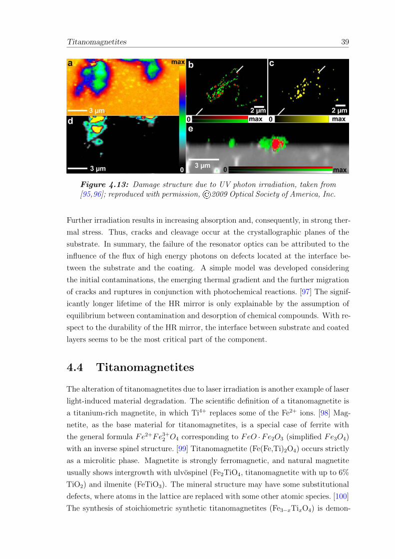
Titanomagnetites 39
Figure 4.13: Damage structure due to UV photon irradiation, taken from[95,96]; reproduced with permission, ©2009 Optical Society of America, Inc.
Further irradiation results in increasing absorption and, consequently, in strong ther-
mal stress. Thus, cracks and cleavage occur at the crystallographic planes of the
substrate. In summary, the failure of the resonator optics can be attributed to the
influence of the flux of high energy photons on defects located at the interface be-
tween the substrate and the coating. A simple model was developed considering
the initial contaminations, the emerging thermal gradient and the further migration
of cracks and ruptures in conjunction with photochemical reactions. [97] The signif-
icantly longer lifetime of the HR mirror is only explainable by the assumption of
equilibrium between contamination and desorption of chemical compounds. With re-
spect to the durability of the HR mirror, the interface between substrate and coated
layers seems to be the most critical part of the component.
4.4 Titanomagnetites
The alteration of titanomagnetites due to laser irradiation is another example of laser
light-induced material degradation. The scientific definition of a titanomagnetite is
a titanium-rich magnetite, in which Ti4+ replaces some of the Fe2+ ions. [98] Mag-
netite, as the base material for titanomagnetites, is a special case of ferrite with
the general formula Fe2+Fe3+2 O4 corresponding to FeO ·Fe2O3 (simplified Fe3O4)
with an inverse spinel structure. [99] Titanomagnetite (Fe(Fe,Ti)2O4) occurs strictly
as a microlitic phase. Magnetite is strongly ferromagnetic, and natural magnetite
usually shows intergrowth with ulvospinel (Fe2TiO4, titanomagnetite with up to 6%
TiO2) and ilmenite (FeTiO3). The mineral structure may have some substitutional
defects, where atoms in the lattice are replaced with some other atomic species. [100]
The synthesis of stoichiometric synthetic titanomagnetites (Fe3−xTixO4) is demon-
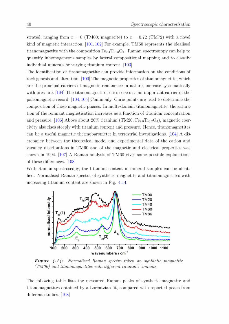
40 Spectroscopic characterisation
strated, ranging from x = 0 (TM00; magnetite) to x = 0.72 (TM72) with a novel
kind of magnetic interaction. [101,102] For example, TM60 represents the idealised
titanomagnetite with the composition Fe2.4Ti0.6O4. Raman spectroscopy can help to
quantify inhomogeneous samples by lateral compositional mapping and to classify
individual minerals or varying titanium content. [103]
The identification of titanomagnetite can provide information on the conditions of
rock genesis and alteration. [100] The magnetic properties of titanomagnetite, which
are the principal carriers of magnetic remanence in nature, increase systematically
with pressure. [104] The titanomagnetite series serves as an important carrier of the
paleomagnetic record. [104,105] Commonly, Curie points are used to determine the
composition of these magnetic phases. In multi-domain titanomagnetite, the satura-
tion of the remnant magnetisation increases as a function of titanium concentration
and pressure. [106] Above about 20% titanium (TM20, Fe2.8Ti0.2O4), magnetic coer-
civity also rises steeply with titanium content and pressure. Hence, titanomagnetites
can be a useful magnetic thermobarometer in terrestrial investigations. [104] A dis-
crepancy between the theoretical model and experimental data of the cation and
vacancy distributions in TM60 and of the magnetic and electrical properties was
shown in 1994. [107] A Raman analysis of TM60 gives some possible explanations
of these differences. [108]
With Raman spectroscopy, the titanium content in mineral samples can be identi-
fied. Normalised Raman spectra of synthetic magnetite and titanomagnetites with
increasing titanium content are shown in Fig. 4.14.
Figure 4.14: Normalised Raman spectra taken on synthetic magnetite(TM00) and titanomagnetites with different titanium contents.
The following table lists the measured Raman peaks of synthetic magnetite and
titanomagnetites obtained by a Lorentzian fit, compared with reported peaks from
different studies. [108]
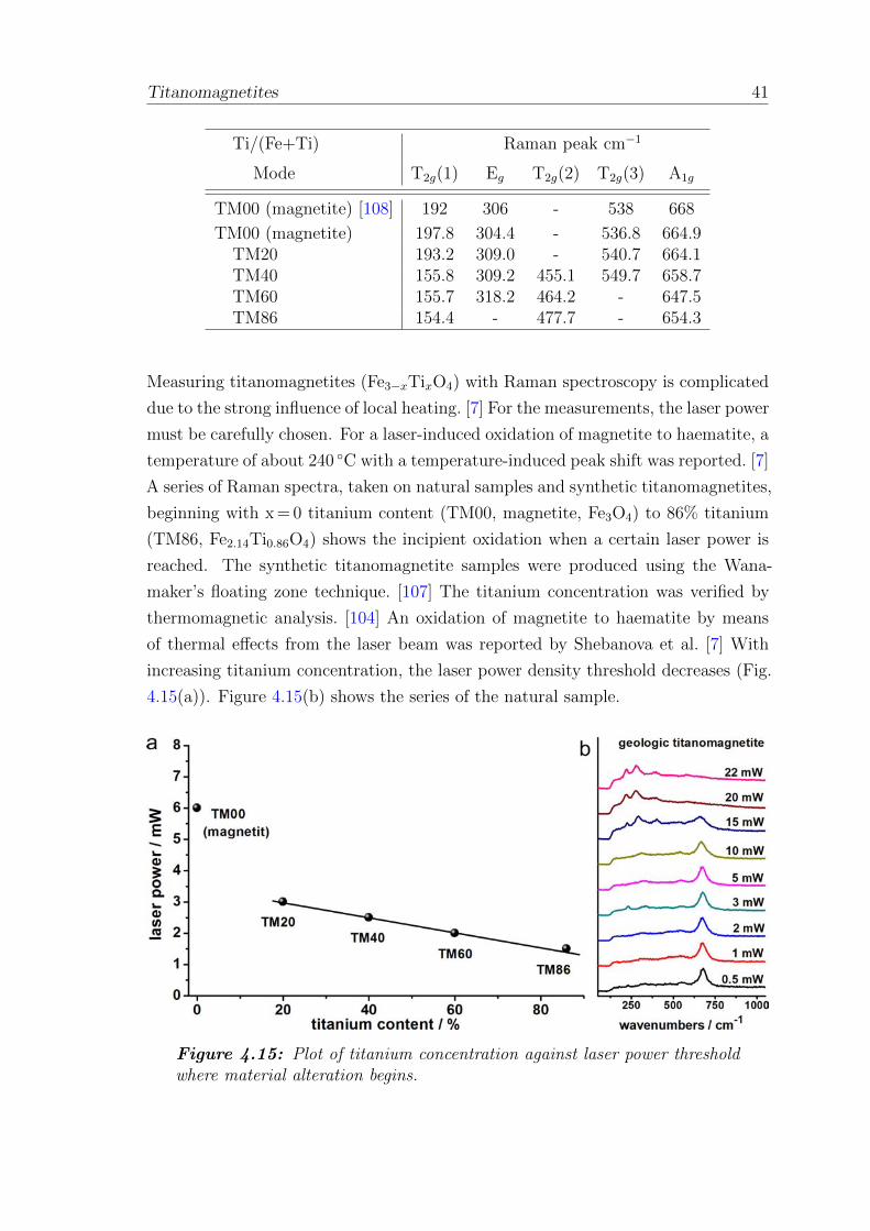
Titanomagnetites 41
Ti/(Fe+Ti) Raman peak cm−1
Mode T2g(1) Eg T2g(2) T2g(3) A1g
TM00 (magnetite) [108] 192 306 - 538 668
TM00 (magnetite) 197.8 304.4 - 536.8 664.9TM20 193.2 309.0 - 540.7 664.1TM40 155.8 309.2 455.1 549.7 658.7TM60 155.7 318.2 464.2 - 647.5TM86 154.4 - 477.7 - 654.3
Measuring titanomagnetites (Fe3−xTixO4) with Raman spectroscopy is complicated
due to the strong influence of local heating. [7] For the measurements, the laser power
must be carefully chosen. For a laser-induced oxidation of magnetite to haematite, a
temperature of about 240 C with a temperature-induced peak shift was reported. [7]
A series of Raman spectra, taken on natural samples and synthetic titanomagnetites,
beginning with x = 0 titanium content (TM00, magnetite, Fe3O4) to 86% titanium
(TM86, Fe2.14Ti0.86O4) shows the incipient oxidation when a certain laser power is
reached. The synthetic titanomagnetite samples were produced using the Wana-
maker’s floating zone technique. [107] The titanium concentration was verified by
thermomagnetic analysis. [104] An oxidation of magnetite to haematite by means
of thermal effects from the laser beam was reported by Shebanova et al. [7] With
increasing titanium concentration, the laser power density threshold decreases (Fig.
4.15(a)). Figure 4.15(b) shows the series of the natural sample.
Figure 4.15: Plot of titanium concentration against laser power thresholdwhere material alteration begins.
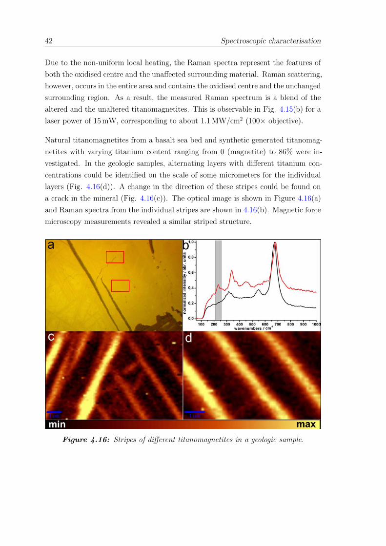
42 Spectroscopic characterisation
Due to the non-uniform local heating, the Raman spectra represent the features of
both the oxidised centre and the unaffected surrounding material. Raman scattering,
however, occurs in the entire area and contains the oxidised centre and the unchanged
surrounding region. As a result, the measured Raman spectrum is a blend of the
altered and the unaltered titanomagnetites. This is observable in Fig. 4.15(b) for a
laser power of 15 mW, corresponding to about 1.1 MW/cm2 (100× objective).
Natural titanomagnetites from a basalt sea bed and synthetic generated titanomag-
netites with varying titanium content ranging from 0 (magnetite) to 86% were in-
vestigated. In the geologic samples, alternating layers with different titanium con-
centrations could be identified on the scale of some micrometers for the individual
layers (Fig. 4.16(d)). A change in the direction of these stripes could be found on
a crack in the mineral (Fig. 4.16(c)). The optical image is shown in Figure 4.16(a)
and Raman spectra from the individual stripes are shown in 4.16(b). Magnetic force
microscopy measurements revealed a similar striped structure.
Figure 4.16: Stripes of different titanomagnetites in a geologic sample.
5 Summary
Confocal Raman spectroscopy is well-suited for the determination of stress fields
generated in the material by means of external applied loading. By analysing the
Raman peaks by means of centre position and width, additional information is acces-
sible. For this purpose, the peaks were fitted with a Lorentzian curve. Stress causes
a peak shift due to affected phonon frequencies. Through the direction of this shift,
compressive and tensile stress can be distinguished. The phonon frequencies vary
not only with stress, but also with changing temperatures. The population of the
phonon branches is mainly influenced by temperature, which leads to an increased
peak width with increased temperature. Due to the diverse impact of mechanical
stress and temperature on the Raman spectra, a separation of both effects is possible.
Depending on light absorption and thermal conductivity, the sample is locally heated
to some degree by the excitation laser, thus introducing additional spectral shifts,
which may require compensation for more precise results. For thermal calibration
purposes, spectral variations were analysed with controlled heating experiments on
single crystals of silicon and different silicon carbide polytypes.
The characterisation of heterogeneous specimens was carried out on outcoupling
resonator mirrors used in excimer lasers that show a UV photon-induced damage at
the exterior surface when a certain energy level is exceeded. The damage structure
was characterised and the components were identified, revealing an alteration of
calcium fluoride bulk material to calcium carbonate (calcite). The particle size was
in the range of a few micrometers in diameter with a depth of about one micrometer
beneath the surface. Little filaments found on samples with the start of surface
damage act as a nucleation point for further damage. The filaments were composed
of organic matter and kerogeneous carbon with small embedded calcite particles.
In addition, geologic samples from a basaltic sea bed with embedded titanomag-
netites were characterised for their composition. Alternating layers with different
titanium ion concentrations could be identified. Synthetic titanomagnetite samples
with known titanium concentrations were used as references to identify the materials.
Significant local heating was observed for all magnetite and titanomagnetite samples.
Above a certain threshold, laser-induced oxidation occurs, which depends on the ti-
43
44 Summary
tanium content. The laser power threshold for the oxidation decreases linearly with
increasing titanium content.
In summary, confocal Raman spectroscopy has great potential to identify substances
and to determine their spatial distribution within a sample. The visualisation of
residual stress fields is another valuable asset. Together with the simple sample
preparation and the possibility for contact-free measurement, confocal Raman spec-
troscopy is a valuable tool for material analysis.
6 References
[1] G. Gouadec and P. Colomban. Raman Spectroscopy of nanomaterials: How
spectra relate to disorder, particle size and mechanical properties. Progress
in Crystal Growth and Characterization of Materials, 53(1):1–56, 2007. doi:
10.1016/j.pcrysgrow.2007.01.001.
[2] S. Nakashima and H. Harima. Raman investigation of SiC polytypes. Phys-
ica Status Solidi a-Applied Research, 162(1):39–64, 1997. doi:10.1002/
1521-396X(199707)162:1<39::AID-PSSA39>3.0.CO;2-L.
[3] I. De Wolf. TOPICAL REVIEW: Micro-Raman spectroscopy to study local
mechanical stress in silicon integrated circuits. Semiconductor Science Tech-
nology, 11:139–154, February 1996. doi:10.1088/0268-1242/11/2/001.
[4] D. G. Mead and G. R. Wilkinson. The temperature dependence of the raman
effect in some wurtzite type crystals. Journal of Raman Spectroscopy, 6(3):123–
129, 1977. doi:10.1002/jrs.1250060305.
[5] T. R. Hart, R. L. Aggarwal, and B. Lax. Temperature Dependence of Raman
Scattering in Silicon. Physical Review B, 1(2):638–642, 1970. doi:10.1103/
PhysRevB.1.638.
[6] N. L. Boling, M. D. Crisp, and G. Dube. Laser Induced Surface Damage. Appl.
Opt., 12(4):650–660, 1973. doi:10.1364/AO.12.000650.
[7] O. N. Shebanova and P. Lazor. Raman study of magnetite (Fe2O3): laser-
induced thermal effects and oxidation. Journal of Raman Spectroscopy,
34(11):845–852, 2003. doi:10.1002/jrs.1056.
[8] C. V. Raman and K. S. Krishnan. A new type of secondary radiation. Nature,
121:501–502, 1928. doi:10.1038/121501c0.
[9] G. Landsberg and L. Mandelstam. A new occurrence in the light diffusion of
crystals. Naturwissenschaften, 16:557–558, 1928.
[10] P. Colomban. Raman analyses and ”smart” imaging of nano-phases and nano-
sized materials. Spectrosc Eur, 16:8–16, 2004.
45
46 Bibliography
[11] D. A. Long. The Raman Effect- A Unified Treatment of the Theory of Raman
Scattering by Molecules. John Wiley & Sons Ltd, West Sussex PO19 1UD,
England, 2002.
[12] M. Cardona and G. Gtintherodt. Light Scattering In Solids VII. Crystal-Field
and Magnetic Excitations. Springer-Verlag, Berlin Heidelberg, 2000.
[13] W. Kaiser and M. Maier. Stimulated Rayleigh, Brillouin, and Raman spec-
troscopy, volume 2 of Laser Handbook. F.T.Arecchi and E.O.Schulz-Dubois,
eds., North-Holland, Amsterdam, 1972.
[14] W.H. Weber and R. Merlin. Raman Scattering in Material Science. Springer
Verlag, Berlin Heidelberg, 2000.
[15] W. J. Miller. Symmetry groups and their applications. ACADEMIC PRESS,
New York, 1972.
[16] K. Dombrowski. Micro-Raman Investigation of Mechanical Stress in Si Device
Structures and Phonons in SiGe. Dissertation, TU-Cottbus, 2000.
[17] W. Hayes. Scattering of Light by Crystals. John Wiley & Sons Inc, New York,
1 st edition, 1978.
[18] D. L. Rousseau, R. P. Bauman, and S. P. S. Porto. Normal Mode Determi-
nation in Crystals. Journal of Raman Spectroscopy, 10(Jan):253–290, 1981.
doi:10.1002/jrs.1250100152.
[19] V. Senez, A. Armigliato, I. De Wolf, G. Carnevale, R. Balboni, S. Frab-
boni, and A. Benedetti. Strain determination in silicon microstructures
by combined convergent beam electron diffraction, process simulation, and
micro-Raman spectroscopy. J. Appl. Phys., 94(9):5574–5583, 2003. doi:
10.1063/1.1611287.
[20] S. M. Hu. Stress-related problems in silicon technology. Journal of Applied
Physics, 70(6):R53–R80, 1991. doi:10.1063/1.349282.
[21] Park H. Jones K.S. Slinkman J.A. Law M.E. The effects of strain on dopant
diffusion in silicon. Proc. 1993. Int. Electron Devices Meeting (IEDM), pages
303–6, 1993. doi:10.1109/IEDM.1993.347347.
[22] I. Neizvestnyi and V. Gridchin. The use of stressed silicon in MOS transistors
and CMOS structures. Russian Microelectronics, 38(2):71–86, 2009. doi:
10.1134/S1063739709020012.
[23] D. W. Feldman, J. H. Parker, W. J. Choyke, and L. Patrick. Phonon Dispersion
Curves by Raman Scattering in SiC Polytypes 3C,4H,6H,15R,and 21R. Phys.
Rev., 173(3):787–793, 1968. doi:10.1103/PhysRev.173.787.
Bibliography 47
[24] D. W. Feldman, J. H. Parker, W. J. Choyke, and L. Patrick. Raman Scattering
in 6H SiC. Phys. Rev., 170(3):698–704, 1968. doi:10.1103/PhysRev.170.698.
[25] J. Menendez and M. Cardona. Temperature-Dependence of the 1st-Order
Raman-Scattering by Phonons in Si, Ge, and a-Sn - Anharmonic Effects. Phys-
ical Review B, 29(4):2051–2059, 1984. doi:10.1103/PhysRevB.29.2051.
[26] G. Lucazeau. Effect of pressure and temperature on Raman spectra of solids:
anharmonicity. J. Raman Spectrosc., 34(7-8):478–496, 2003. doi:10.1002/
jrs.1027.
[27] S. Ganesan, A. A. Maradudin, and J. Oitmaa. A lattice theory of morphic
effects in crystals of the diamond structure. Annals of Physics, 56(2):556–594,
1970. doi:10.1016/0003-4916(70)90029-1.
[28] E. Anastassakis, A. Pinczuk, E. Burstein, F. H. Pollak, and M. Cardona.
Effect of static uniaxial stress on the Raman spectrum of silicon. Solid State
Communications, 8(2):133–138, 1970. doi:10.1016/0038-1098(70)90588-0.
[29] Xiaoming Wu, Jianyuan Yu, Tianling Ren, and Litian Liu. Micro-Raman spec-
troscopy measurement of stress in silicon. Microelectronics Journal, 38(1):87–
90, 2007. doi:10.1016/j.mejo.2006.09.007.
[30] A. B. Horsfall, J. M. M. d. Santos, S. M. Soare, N. G. Wright, A. G. O’Neill,
S. J. Bull, A. J. Walton, A. M. Gundlach, and J. T. M. Stevenson. Direct
measurement of residual stress in sub-micron interconnects. Semicond. Sci.
Technol., 18(11):992–996, 2003. doi:10.1088/0268-1242/18/11/315.
[31] S. Kouteva-Arguirova, T. Arguirov, D. Wolfframm, and J. Reif. Influence
of local heating on micro-Raman spectroscopy of silicon. Journal of Applied
Physics, 94(8):4946–4949, 2003. doi:10.1063/1.1611282.
[32] B. A. Weinstein and G. J. Piermarini. Raman-Scattering and Phonon Disper-
sion in Si and Gap at very High-Pressure. Physical Review B, 12(4):1172–1186,
1975. doi:10.1103/PhysRevB.12.1172.
[33] T. Beechem, S. Graham, S. P. Kearney, L. M. Phinney, and J. R. Serrano.
Simultaneous mapping of temperature and stress in microdevices using micro-
Raman spectroscopy. Review of Scientific Instruments, 78(6), 2007. doi:
10.1063/1.2738946.
[34] C. Ulrich, A. Debernardi, E. Anastassakis, K. Syassen, and M. Cardona.
Raman linewidths of phonons in Si, Ge, and SiC under pressure. Physica
Status Solidi B-Basic Research, 211(1):293–300, 1999. doi:10.1002/(SICI)
1521-3951(199901)211:1<293::AID-PSSB293>3.0.CO;2-O.
48 Bibliography
[35] J. Liu and Y. K. Vohra. Raman Modes of 6H Polytype of Silicon-Carbide to Ul-
trahigh Pressures - a Comparison with Silicon and Diamond. Physical Review
Letters, 72(26):4105–4108, 1994. doi:10.1103/PhysRevLett.72.4105.
[36] J. Liu and Y. K. Vohra. Raman modes of 6H polytype of silicon carbide to
ultrahigh pressures - Reply. Physical Review Letters, 77(8):1661–1661, 1996.
[37] A. Debernardi and M. Cardona. Dependence of phonon linewidths in semicon-
ductors on temperature and isotopic composition. Nuovo Cimento D Serie,
20(7-8):923–930, 1998.
[38] A. Debernardi, C. Ulrich, K. Syassen, and M. Cardona. Raman linewidths
of optical phonons in 3C-SiC under pressure: First-principles calculations and
experimental results. Physical Review B, 59(10):6774–6783, 1999. doi:10.
1103/PhysRevB.59.6774.
[39] A. Debernardi, C. Ulrich, M. Cardona, and K. Syassen. Pressure depen-
dence of Raman linewidth in semiconductors. Physica Status Solidi B-
Basic Research, 223(1):213–223, 2001. doi:10.1002/1521-3951(200101)
223:1<213::AID-PSSB213>3.0.CO;2-I.
[40] D. Olego and M. Cardona. Temperature-Dependence of the Optical Phonons
and Transverse Effective Charge in 3C-SiC. Physical Review B, 25(6):3889–
3896, 1982. doi:10.1103/PhysRevB.25.3889.
[41] R. Jalilian, G. U. Sumanasekera, H. Chandrasekharan, and M. K. Sunkara.
Phonon confinement and laser heating effects in Germanium nanowires. Phys-
ical Review B (Condensed Matter and Materials Physics), 74(15):155421, 2006.
doi:10.1103/PhysRevB.74.155421.
[42] Z. Li and R. C. Bradt. Thermal-Expansion and Thermal-Expansion
Anisotropy of SiC Polytypes. Journal of the American Ceramic Society,
70(7):445–448, 1987. doi:10.1111/j.1151-2916.1987.tb05673.x.
[43] R. Zallen and M. L. Slade. Influence of pressure and temperature on phonons
in molecular chalcogenides: Crystalline As4S4 and S4N4. Phys. Rev. B,
18(10):5775–5798, Nov 1978. doi:10.1103/PhysRevB.18.5775.
[44] A. Sen, S.L. Chaplot, and R. Mittal. Effects of pressure and temperature on
the vibronic as well as the thermodynamic properties of LiYF4 and LiYbF4.
Journal of Physics Condensed Matter, 14:975–986, February 2002. doi:10.
1088/0953-8984/14/5/303.
[45] R. Passler. Moderate phonon dispersion shown by the temperature dependence
of fundamental band gaps of various elemental and binary semiconductors
Bibliography 49
including wide-band gap materials. Journal of Applied Physics, 88(5):2570–
2577, 2000. doi:10.1063/1.1287601.
[46] A. Compaan and H. J. Trodahl. Resonance Raman-Scattering in Si at
Elevated-Temperatures. Physical Review B, 29(2):793–801, 1984. doi:10.
1103/PhysRevB.29.793.
[47] M. Balkanski, R. F. Wallis, and E. Haro. Anharmonic Effects in Light-
Scattering due to Optical Phonons in Silicon. Physical Review B, 28(4):1928–
1934, 1983. doi:10.1103/PhysRevB.28.1928.
[48] S. A. Hambir, J. Franken, D. E. Hare, E. L. Chronister, B. J. Baer, and D. D.
Dlott. Ultrahigh time-resolution vibrational spectroscopy of shocked molecular
solids. J. Appl. Phys., 81(5):2157–2166, 1997. doi:10.1063/1.364269.
[49] H. Harima, S. Nakashima, and T. Uemura. Raman-Scattering from
Anisotropic LO-Phonon-Plasmon-Coupled Mode in N-Type 4H-SiC and 6H-
SiC. J. Appl. Phys., 78(3):1996–2005, 1995. doi:10.1063/1.360174.
[50] M. R. Abel, S. Graham, J. R. Serrano, S. P. Kearney, and L. M. Phinney. Ra-
man thermometry of polysilicon microelectromechanical systems in the pres-
ence of an evolving stress. Journal of Heat Transfer-Transactions of the Asme,
129(3):329–334, 2007. doi:10.1115/1.2409996.
[51] R. Tsu and J. G. Hernandez. Temperature-Dependence of Silicon Raman Lines.
Applied Physics Letters, 41(11):1016–1018, 1982. doi:10.1063/1.93394.
[52] J. W. Pomeroy, M. Kuball, H. Lu, W. J. Schaff, X. Wang, and A. Yoshikawa.
Phonon lifetimes and phonon decay in InN. Applied Physics Letters,
86(22):223501, 2005. doi:10.1063/1.1940124.
[53] Leah Bergman, Michael D. Bremser, William G. Perry, Robert F. Davis, Mi-
tra Dutta, and Robert J. Nemanich. Raman analysis of the configurational
disorder in AlxGa1−xN films. Applied Physics Letters, 71(15):2157–2159, 1997.
doi:10.1063/1.119367.
[54] Olaf Hollricher Wolfram Ibach. High Resolution Optical Microscopy. WITec,
Jungingen, 2002.
[55] E. Hering and R. Martin. Photonik: Grundlagen, Technologie und Anwendung.
Springer, Berlin, Berlin, 2006.
[56] H. W. Lo and A. Compaan. Raman Measurements of Temperature during
cw Laser-Heating of Silicon. J. Appl. Phys., 51(3):1565–1568, 1980. doi:
10.1063/1.327809.
50 Bibliography
[57] H. W. Lo and A. Compaan. Raman Measurement of Lattice Temperature
during Pulsed Laser Heating of Silicon. Physical Review Letters, 44(24):1604,
1980. doi:10.1103/PhysRevLett.44.1604.
[58] P. E. Van Camp, V. E. Van Doren, and J. T. Devreese. Microscopic Screening
and Phonon Dispersion of Silicon: Moment Expansion for the Polarizability.
Phys. Rev. Lett., 42(18):1224, 1979. doi:10.1103/PhysRevLett.42.1224.
[59] Wikipedia. Silicium - Wikipedia, Die freie Enzyklopadie, 2009. [accessed 8-
December-2009]. Available from: http://de.wikipedia.org/w/index.php?
title=Silicium&oldid=67689997.
[60] D. E. Aspnes and A. A. Studna. Dielectric functions and optical parameters
of Si, Ge, GaP, GaAs, GaSb, InP, InAs, and InSb from 1.5 to 6.0 eV. Phys.
Rev. B, 27(2):985, Jan 1983. doi:10.1103/PhysRevB.27.985.
[61] Kohji Mizoguchi and Shin ichi Nakashima. Determination of crystallographic
orientations in silicon films by Raman-microprobe polarization measurements.
Journal of Applied Physics, 65(7):2583–2590, 1989. doi:10.1063/1.342787.
[62] M. Bauer, A. M. Gigler, C. Richter, and R. W. Stark. Visualizing stress in
silicon micro cantilevers using scanning confocal Raman spectroscopy. Micro-
electron. Eng., 85(5-6):1443–1446, 2008. doi:10.1016/j.mee.2008.01.089.
[63] J. B. Casady and R. W. Johnson. Status of silicon carbide (SiC) as a wide-
bandgap semiconductor for high-temperature applications: A review. Solid-
State Electr., 39(10):1409–1422, 1996. doi:10.1016/0038-1101(96)00045-7.
[64] J. Baliga. Silicon Carbide Power Devices. Worlds Scientific Publishing Co.
Pte. Ltd., Singapore, 2005.
[65] J. S. Sullivan and J. R. Stanley. 6H-SiC photoconductive switches triggered at
below bandgap wavelengths. Ieee Transactions on Dielectrics and Electrical
Insulation, 14(4):980–985, 2007. doi:10.1109/TDEI.2007.4286537.
[66] Z. Li and R. C. Bradt. Thermal-Expansion of the Hexagonal (4H) Polytype
of SiC. J. Appl. Phys., 60(2):612–614, 1986. doi:10.1063/1.337456.
[67] O. Kordina. Growth and characterisation of silicon carbide power device ma-
terial. Dissertation, Linkoping University, 1994.
[68] Olle Kordina. General Properties of Silicon Carbide, 2009. [accessed
8-December-2009]. Available from: http://www.ifm.liu.se/matephys/
AAnew/research/sicpart/kordina2.htm.
Bibliography 51
[69] J. C. Burton, L. Sun, M. Pophristic, S. J. Lukacs, F. H. Long, Z. C. Feng,
and I. T. Ferguson. Spatial characterization of doped SiC wafers by Raman
spectroscopy. Journal of Applied Physics, 84(11):6268–6273, 1998. doi:10.
1063/1.368947.
[70] K. Karch, P. Pavone, W. Windl, O. Schutt, and D. Strauch. Ab initio calcu-
lation of structural and lattice-dynamical properties of silicon carbide. Phys.
Rev. B, 50(23):17054 – 17063, Dec 1994. doi:10.1103/PhysRevB.50.17054.
[71] Z. Li and R. C. Bradt. Thermal-Expansion of the Cubic (3C) Polytype of SiC.
J. Mat. Science, 21(12):4366–4368, 1986. doi:10.1007/BF01106557.
[72] H. Harima, T. Hosoda, and S. Nakashima. Temperature measurement in a
silicon carbide light emitting diode by Raman scattering. Journal of Electronic
Materials, 28(3):141–143, 1999. doi:10.1007/s11664-999-0003-4.
[73] Z. Li and R. C. Bradt. Thermal-Expansion of the Hexagonal (6H) Polytype
of Silicon-Carbide. Journal of the American Ceramic Society, 69(12):863–866,
1986. doi:10.1111/j.1151-2916.1986.tb07385.x.
[74] J. C. Burton, L. Sun, F. H. Long, Z. C. Feng, and I. T. Ferguson. First- and
second-order Raman scattering from semi-insulating 4H-SiC. Physical Review
B, 59(11):7282–7284, 1999. doi:10.1103/PhysRevB.59.7282.
[75] S. Nakashima, T. Mitani, J. Senzaki, H. Okumura, and T. Yamamoto. Deep
ultraviolet Raman scattering characterization of ion-implanted SiC crystals.
Journal of Applied Physics, 97(12), 2005. doi:10.1063/1.1931039.
[76] M. Bauer, A.M. Gigler, A.J. Huber, R. Hillenbrand, and R.W. Stark.
Temperature-depending raman line-shift of silicon carbide. Journal of Raman
Spectroscopy, 40(12):1867–1874, 2009. doi:10.1002/jrs.2334.
[77] Alexander M. Gigler, Andreas J. Huber, Michael Bauer, Alexander Ziegler,
Rainer Hillenbrand, and Robert W. Stark. Nanoscale residual stress-field
mapping around nanoindents in SiC by IR s-SNOM and confocal Raman mi-
croscopy. Optics Express, 17(25):22351–22357, 2009. doi:10.1364/OE.17.
022351.
[78] A. L. Espana, A. G. Joly, W. P. Hess, and J. T. Dickinson. Laser-Induced Dam-
age of Calcium Fluoride. Journal Name: Journal of Undergraduate Research;
Journal Volume: 4, page Medium: X, 2004.
[79] J. H. Apfel, E. A. Enemark, D. Milam, W. L. Smith, and M. J. Weber. Effects
of barrier layers and surface smoothness on 150-ps, 1.064 µm laser damage of
AR coatings on glass. page p. 255, United States, 1977. NIST Spec. Pub. 5009.
52 Bibliography
[80] V. Liberman, M. Rothschild, J. H. C. Sedlacek, R. S. Uttaro, A. Grenville,
A. K. Bates, and C. Van Peski. Excimer-laser-induced degradation of fused
silica and calcium fluoride for 193-nm lithographic applications. Optics Letters,
24(1):58–60, 1999. doi:10.1364/OL.24.000058.
[81] T. Feigl, J. Heber, A. Gatto, and N. Kaiser. Optics developments in the
VUV - soft X-ray spectral region. Nuclear Instruments & Methods in Physics
Research Section a-Accelerators Spectrometers Detectors and Associated Equip-
ment, 483(1-2):351–356, 2002. doi:10.1016/S0168-9002(01)00060-2.
[82] W. Arens, D. Ristau, J. Ullmann, C. Zaczek, R. Thielsch, N. Kaiser, A. Du-
parre, O. Apel, R. Mann, K., H. Lauth, H. Bernitzki, J. Ebert, S. Schippel,
and H. Heyer. Properties of fluoride DUV excimer laser optics: influence of
the number of dielectric layers. In Laser-Induced Damage in Optical Materials:
1999, volume 3902, pages 250–259. SPIE, 2000. doi:10.1117/12.379314.
[83] M. Marsi, A. Locatelli, M. Trovo, R. P. Walker, M. E. Couprie, D. Garzella,
L. Nahon, D. Nutarelli, E. Renault, A. Gatto, N. Kaiser, L. Giannessi, S. Gun-
ster, D. Ristau, M. W. Poole, and A. Taleb-Ibrahimi. UV/VUV free electron
laser oscillators and applications in materials science. Surface Review and
Letters, 9(1):599–607, 2002. doi:10.1142/S0218625X02001768.
[84] D. Ristau, W. Arens, S. Bosch, A. Duparre, E. Masetti, D. Jacob, G. Kiriakidis,
F. Peiro, E. Quesnel, and A. V. Tikhonravov. UV-optical and microstructural
properties of MgF2-coatings deposited by IBS and PVD processes. In Advances
in Optical Interference Coatings, volume 3738, pages 436–445. SPIE, 1999.
[85] Korth Kristalle GmbH. CALCIUM FLUORIDE, 2009. [accessed 8-December-
2009]. Available from: http://korth.de/eng/503728952d091450d/
503728952d09c361d.htm.
[86] V. Liberman, M. Switkes, M. Rothschild, S. T. Palmacci, J. H. C. Sedlacek,
D. E. Hardy, and A. Grenville. Long-term 193-nm laser irradiation of thin-
film-coated CaF2 in the presence of H2O. In Bruce W. Smith, editor, Optical
Microlithography XVIII, volume 5754, pages 646–654. SPIE, 2004. doi:10.
1117/12.601468.
[87] V. Liberman, M. Rothschild, S. T. Palmacci, Ni. N. Efremow, J. H. C. Sedlacek,
and A. Grenville. Ambient effects on the laser durability of 157-nm optical
coatings. In Anthony Yen, editor, Optical Microlithography XVI, volume 5040,
pages 487–498. SPIE, 2003. doi:10.1117/12.497525.
[88] L.Parthier. Immersion Lithography: a new challenge for CaF2 quality. In Op-
tical Microlithography XVIII, volume 5754, pages presented, but unpublished
in Proc. SPIE, 2005.
Bibliography 53
[89] J. W. Schopf, A. B. Kudryavtsev, D. G. Agresti, T. J. Wdowiak, and A. D.
Czaja. Laser-Raman imagery of Earth’s earliest fossils. Nature, 416(6876):73–
76, 2002. doi:10.1038/416073a.
[90] O. Beyssac, J.-N. Rouzaud, B. Goffe, F. Brunet, and C. Chopin. Graphitiza-
tion in a high-pressure, low-temperature metamorphic gradient: a Raman mi-
crospectroscopy and HRTEM study. Contributions to Mineralogy and Petrol-
ogy, 143(1):19–31, 2002. doi:10.1007/s00410-001-0324-7.
[91] O. Beyssac, B. Goffe, C. Chopin, and J. N. Rouzaud. Raman spectra of
carbonaceous material in metasediments: a new geothermometer. Journal
of Metamorphic Geology, 20(9):859–871, 2002. doi:10.1046/j.1525-1314.
2002.00408.x.
[92] O. Beyssac, B. Goffe, J.-P. Petitet, E. Froigneux, M. Moreau, and J.-N.
Rouzaud. On the characterization of disordered and heterogeneous carbona-
ceous materials by Raman spectroscopy. Spectrochimica Acta Part A: Molec-
ular and Biomolecular Spectroscopy, 59(10):2267–2276, 2003. doi:10.1016/
S1386-1425(03)00070-2.
[93] A. Cuesta, P. Dhamelincourt, J. Laureyns, A. Martinez-Alonso, and J. M. D.
Tascon. Comparative performance of X-ray diffraction and Raman microprobe
techniques for the study of carbon materials. Journal of Materials Chemistry,
8(12):2875–2879, 1998. doi:10.1039/a805841e.
[94] C. Beny-Bassez and J.N. Rouzaud. Scanning Electron Microscopy. AMF
O’Hare (Ed.), SEM Inc., Chicago, 1985.
[95] M. Bauer, M. Bischoff, S. Jukresch, T. Hulsenbusch, A. Matern, A. Gortler,
R. W. Stark, A. Chuvilin, and U. Kaiser. Exterior surface damage of calcium
fluoride outcoupling mirrors for DUV lasers. Opt. Express, 17(10):8253–8263,
2009. doi:10.1364/OE.17.008253.
[96] Michael Bauer, Martin Bischoff, Thomas Hulsenbusch, Ansgar Matern,
Robert W. Stark, and Norbert Kaiser. Onset of the optical damage in
CaF2 optics caused by deep-UV lasers. Opt. Lett., 34(24):3815–3817, 2009.
doi:10.1364/OL.34.003815.
[97] N. Beermann, H. Blaschke, H. Ehlers, D. Ristau, D. Wulff-Molder, S. Jukresch,
A. Matern, C. F. Strowitzki, A. Gortler, M. B. Gabler, and N. Kaiser. Long
Term Tests of Resonator Optics in ArF Excimer Lasers. In XVII International
Symposium on Gas Flow and Chemical Lasers & High Power Lasers 2008,
Lisbon, Portugal, 2008. doi:10.1117/12.816706.
[98] D. H. Lindsley. Experimental Studies of Oxide Minerals. Reviews in Mineral-
ogy, 25:69–106, 1991.
54 Bibliography
[99] L. V. Gasparov, D. B. Tanner, D. B. Romero, H. Berger, G. Margaritondo, and
L. Forro. Infrared and Raman studies of the Verwey transition in magnetite.
Phys. Rev. B, 62(12):7939–7944, Sep 2000. doi:10.1103/PhysRevB.62.7939.
[100] A. Wang, K. E. Kuebler, B. L. Jolliff, and L. A. Haskin. Raman spectroscopy
of Fe-Ti-Cr-oxides, case study: Martian meteorite EETA79001. American
Mineralogist, 89(5-6):665–680, 2004.
[101] H. C. Soffel and E. Appel. Domain structure of small synthetic titanomagnetite
particles and experiments with IRM and TRM. Physics of The Earth and Plan-
etary Interiors, 30(4):348–355, 1982. doi:10.1016/0031-9201(82)90042-5.
[102] M. Lewis. Some Experiments on Synthetic Titanomagnetites. Geophysical
Journal of the Royal Astronomical Society, 16(3):295–310, 1968. doi:10.
1111/j.1365-246X.1968.tb00224.x.
[103] T. Dorfer, W. Schumacher, N. Tarcea, M. Schmitt, and J. Popp. Quantitative
mineral analysis using raman spectroscopy and chemometric techniques. Jour-
nal of Raman Spectroscopy, 9999(9999):n/a, 2009. doi:10.1002/jrs.2503.
[104] S. A. Gilder and M. Le Goff. Systematic pressure enhancement of titano-
magnetite magnetization. Geophys. Res. Lett., 35, 2008. doi:10.1029/
2008GL033325.
[105] M. Marshall and A. Cox. Effect of Oxidation on the Natural Remanent Mag-
netization of Titanomagnetite in Suboceanic Basalt. Nature, 230(5288):28–31,
1971. doi:10.1038/230028a0.
[106] Gary D. Storrick. Thermoremanent behaviour of small multidomain synthetic
Magnetites. Dissertation, University of Pittsburgh, 1993.
[107] B. J. Wanamaker and B. M. Moskowitz. Effect of Nonstoichiometry on the
Magnetic and Electrical Properties of Synthetic Single Crystal Fe2.4Ti0.6O4.
Geophys. Res. Lett., 21:983–986, 1994. doi:10.1029/94GL00877.
[108] Olga N. Shebanova and Peter Lazor. Raman spectroscopic study of magnetite
(FeFe2O4): a new assignment for the vibrational spectrum. J. Solid State
Chem., 174(2):424–430, 2003. doi:10.1016/S0022-4596(03)00294-9.
7 Publications
7.1 Visualizing stress in silicon microcantilevers
using scanning confocal Raman spectroscopy
M. Bauer, A.M. Gigler, C. Richter, R.W. Stark
Microelectronic Engineering, Volume 85, Issues 5 - 6, Pages 1443 - 1446
Proceedings of the Micro- and Nano-Engineering 2007 Conference - MNE 2007
Permanent weblink:
http://dx.doi.org/10.1016/j.mee.2008.01.089
55

56 Microelectronic Engineering
!"#$"%&'%()#'*+,"#+")#-."/)%$0"#$'&1)%$2)#-1#3,%'#0"#$)4*+,"#+"5678-9,:;<)=,0,4,)#5;>#,3"%5,$)?$<8?#+2"#6@ABBB<8#,+26C"%0)#D()#'E'%4-*"%3,+"5C0FG6HIAJ@1%4)#:"#6C"%0)#DKLM NOOPQKK LRSNOOTQKLPSNOOT TUNOOTVWXYZ[\Y K ] U KK _ K KKKK] K K a K K K K K] b K K KKK b K Kcb Kdeffghijklmknopqpriinmstujnkjknlkvpw"D9'%-5x Q QQ QyKKQz Q |~YZ\Y~ ]K LNK K]K K_ K Ry KK]K KK]K] Ky K K KKK _ K K K K KKKc y KK K K U K K a K K ]K a K K K K ] ] K KKK K K a ]KK K U K R NLL Ly_ b y OLP]LP] dNOOTKK LOLOLNOOTOLOT K yRTNLTORN1;0),4)--%"55x]K ¡¢ £¤¥¦§¥§©ª«¬§¦¬©ª¥ª®®®°±¦©¬±©²¦³©±±« TNOOTLRRµLRR
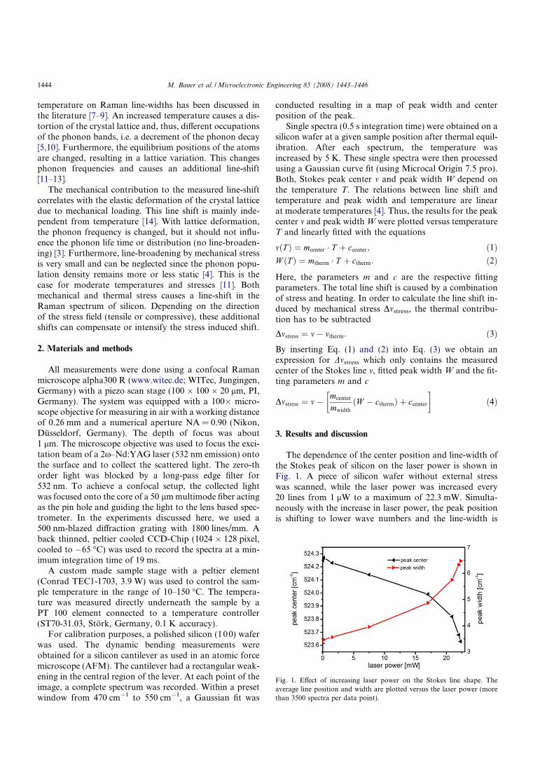
!"##$%#"&% #%'("#)*#+&!#$#'%,-#.*$+/012345627829:;43<=:8 #& * >(?%@##A+ B#* C CD EF?A+% " CG$# H# DIJK *JH-LA+% E%G$ MDNJOPA*&D+#%B# H##.&D%$# E.####?M B## Q RHSS-S* D'CDQMTIUS+ # # *S%VS &&(+ # US% F% *W% & &WLHA X+!* + %# $*!Y+%$# H##$# ( ' T TA. #H HW#* #+ #$" X%# #A$.*#YZ#+,WHH[H \ ]% H '%H[H \ $]. "[_ abc_def g _ abc_deh Dijk$.#%#?l[l[a[T[h &,#V"*+*D+V"*&+ Mm[ WH[.H \.#jkl[a[T bb gTe den o 'p0q48r73829::68sr886=9% WHH !# M $D E( MDD&(W H# $ !#V# WH%$# $ *& +''' tuvwxyzyw|ut~kzy|ykz~k~yyz~
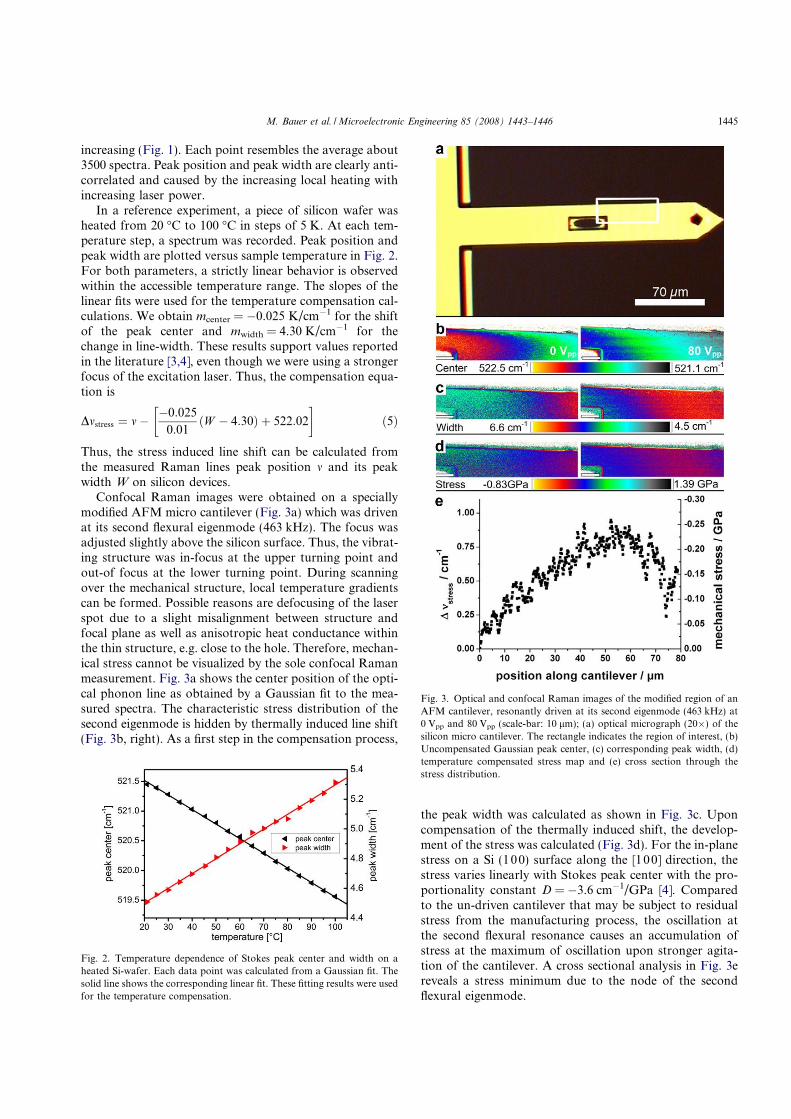
!"#!!!$%&%&!'(#$#)!*!+,-.$'/.!!!,-0'/. !)1#02#!!")#34565. .7$7 89.07:;$$7$< = 8:)#!!>5? &!>*(@A"0BCD)!E!)#!!!F#!!!!#)!#D!>!G*)!!#(*# H!!#!I!12#IJ-.B./G102&E!!#A"!"!!(!A"$)!II! !G*)*)*! K!>!*!(@ #0BCDLMLNOP$Q!)!#HG##RSTUVWXWYUZS[R\]XWZW]YX_\] _a\_WWX\_abcdeffbghiijkhiil 00
!"#$%&'("#) * + ,* - , ./0, )1 12 1 3$4#"5%678696#:'2+- ;<=/>?<,@AA?ABCDE?F,GH6I6J6#$6'KBLM2NN,BBF@GFBOODGBCOPBQ?K@LRN+.SN/NTU N/NV/NB@FDGF@AACGWWOPWEWKCLNS.,.M2*V)V.>O?FEGF@AACG?O?DP?O?OK?L,NUN>SX/>V)N)NWEFDGF@AAWGADBCABKQL),VUY.>X?BFBBGFBOE@GBABDPBABEKDLSM + ,T< [email protected] V+M;Y;X<VMMMV.>EBFQGFBOOWG@BQWP@BDDKELM;YV+MMMV.>WWFBBGFBOOQGQOQAPQODAKOL/). NUV)NN>SX/>VY,B@OFCGF@AAWGC@OPCC?KBAL.<YV,>)@OF@GFBOE?GWOCPEABKBBLUXV)NC?FWPEGF@AACG?WEP?ODKB@LV//<>) @OF?GFBOE?G@AQBP@AQOKBCL,)Y)X.X>)BF@GFBOWAGDCEPD?@KB?L.2UV>>)B@F?GFBOWQGBBW@PBBEDB??D Z[\]__a]b[cZdef_b_eafgdehgidg__dgijklmnnjopqqrspqqt
Journal of Raman Spectroscopy 61
7.2 Temperature depending Raman line-shift of
silicon carbide
Michael Bauer, Alexander M. Gigler, Andreas J. Huber, Rainer Hillenbrand
and Robert W. Stark
Journal of Raman Spectroscopy, 2009, Volume 40 Issue 12, Pages 1867 - 1874
Permanent weblink:
http://dx.doi.org/10.1002/jrs.2334

62 Journal of Raman Spectroscopy
18
67
Research ArticleReceived: 18 December 2008 Accepted: 31 March 2009 Published online in Wiley Interscience: 11 May 2009
(www.interscience.wiley.com) DOI 10.1002/jrs.2334
Temperature-depending Raman line-shiftof silicon carbideMichael Bauer,a,b Alexander M. Gigler,a,b Andreas J. Huber,b,c
Rainer Hillenbrandb,c and Robert W. Starka,b∗
Silicon carbide (SiC) is often used for electronic devices operating at elevated temperatures. Spectroscopic temperaturemeasurements are of high interest for device monitoring because confocal Raman microscopy provides a very high spatialresolution. To this end, calibration data are needed that relate Raman line-shift and temperature. The shift of the phononwavenumbers of single crystal SiC was investigated by Raman spectroscopy in the temperature range from 3 to 112 C. Spectrawere obtained in undoped 6H–SiC as well as in undoped and nitrogen-doped 4H–SiC. All spectra were acquired with theincident laser beam oriented parallel as well as perpendicular to the c-axis to account for the anisotropy of the phonondispersion. Nearly all individual peak centers were shifting linearly towards smaller wavenumbers with increasing temperature.Only the peak of the longitudinal optical phonon A1(LO) in nitrogen-doped 4H–SiC was shifting to larger wavenumbers. For allphonons, a linear dependence of the Raman peaks on both parameters, temperature and phonon frequency, was found in thegiven temperature range. The linearity of the temperature shift allows for precise spectroscopic temperature measurements.Temperature correction of Raman line-shifts also provides the ability to separate thermal shifts from mechanically inducedones. Copyright c© 2009 John Wiley & Sons, Ltd.
Keywords: silicon carbide; temperature; Raman line-shift
Introduction
Silicon carbide (SiC) is a semiconductor that can be used for high-temperature and high-voltage applications. Local temperatureand stress measurements are needed for the optimization offabrication processes and to monitor the devices during operation.Raman spectroscopy is a powerful tool for such measurementsin crystalline materials by analyzing line-shift and shape of theRaman peaks.[1,2] A shift of the phonon peaks can be inducedby temperature changes or mechanical stress. Thus, a precisetemperature calibration allows one to separate both effects andto achieve compensated values for local temperature and stressmeasurements under typical operational conditions of about −20to +120 C.
Raman spectra of crystalline materials depend on the inelasticscattering of light at phonons and consequently on the phononband structure of the lattice.[3] This relationship can give directaccess to the phonon band structure of SiC single crystals.[4,5] SiCpolytypes are named according to the number n of double layersin their unit cell followed by the lattice type (C, H, R) with cubic3C–SiC being the most basic structure. For each polytype, thelength of the unit cell along the c-axis is n times larger than that ofthe basic 3C–SiC type. Due to this increased unit cell, the Brillouinzone is decreased in the –L direction to 1/n coinciding with areduced wavevector (x = q/qB) of the phonon mode in the basicBrillouin zone (q = 0). For higher order polytypes, the dispersioncurves of the propagating phonons are folded backwards into thebasic zone creating additional phonon modes, usually referred toas folded modes.[6,7]
Raman spectroscopy can also be used to measure thedistribution of dopants within polar semiconductors.[6] Dependingon the nitrogen concentration in SiC, width, spectral shape,and peak position of the longitudinal optical phonon A1(LO)
phonon change. These variations have been attributed toplasmon–phonon coupling.[6,8] Nitrogen doping of SiC generatesfree carriers in the semiconductor. Light can excite oscillations ofthese free carriers (plasmons) that can couple to the longitudinaloptical phonons leading to a plasmon–phonon coupled LO mode(LOPC). The frequency and line-shape of the LOPC peak canbe described analytically based on the dielectric function.[6,9] TheLOPC line allows one to measure carrier density and mobility.[10 – 13]
Its line-shift can be used to characterize ion-implanted SiCwith different annealing temperatures to deduce the free-carrierdensity[13,14] and the spatial distribution of the dopants.[6]
Increasing temperature causes a distortion of the lattice andthus, a change in population of the phonon bands that resultsin relative line-shifts and line-broadening.[15,16] Due to the linearexpansion of the equilibrium position of the atoms, the bondstrength changes for moderate temperatures.[17] This modifies thephonon wavenumbers and leads to a shift of the correspondingRaman peaks. The anisotropy of thermal expansion of SiC showsa non-linear behavior for high temperatures giving rise to varyinglattice parameters as well as unit cell vectors.[18,19]
The temperature-induced shift of the peak position in Ramanspectra can be used for local temperature measurements as it was
∗ Correspondence to: Robert W. Stark, Department of Earth and EnvironmentalSciences, Ludwig-Maximilians-Universitat Munchen, Theresienstr. 41, 80333Munich, Germany. E-mail: [email protected]
a Department of Earth and Environmental Sciences, Ludwig-Maximilians-Universitat Munchen, Theresienstr. 41, 80333 Munich, Germany
b Center for NanoScience (CeNS), Schellingstr. 4, 80799 Munich, Germany
c Nanooptics Laboratory, CIC nanoGUNE, 20009 Donostia – San Sebastian, Spain
J. Raman Spectrosc. 2009, 40, 1867–1874 Copyright c© 2009 John Wiley & Sons, Ltd.
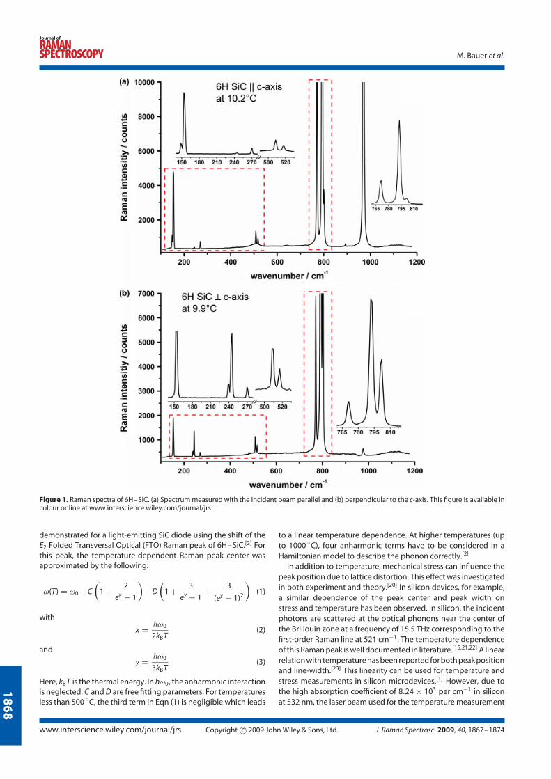
18
68
M. Bauer et al.
Figure 1. Raman spectra of 6H–SiC. (a) Spectrum measured with the incident beam parallel and (b) perpendicular to the c-axis. This figure is available incolour online at www.interscience.wiley.com/journal/jrs.
demonstrated for a light-emitting SiC diode using the shift of theE2 Folded Transversal Optical (FTO) Raman peak of 6H–SiC.[2] Forthis peak, the temperature-dependent Raman peak center wasapproximated by the following:
ω(T) = ω0 − C
(1 + 2
ex − 1
)− D
(1 + 3
ey − 1+ 3
(ey − 1)2
)(1)
with
x = ω0
2kBT(2)
and
y = ω0
3kBT(3)
Here, kBT is the thermal energy. In hω0, the anharmonic interactionis neglected. C and D are free fitting parameters. For temperaturesless than 500 C, the third term in Eqn (1) is negligible which leads
to a linear temperature dependence. At higher temperatures (upto 1000 C), four anharmonic terms have to be considered in aHamiltonian model to describe the phonon correctly.[2]
In addition to temperature, mechanical stress can influence thepeak position due to lattice distortion. This effect was investigatedin both experiment and theory.[20] In silicon devices, for example,a similar dependence of the peak center and peak width onstress and temperature has been observed. In silicon, the incidentphotons are scattered at the optical phonons near the center ofthe Brillouin zone at a frequency of 15.5 THz corresponding to thefirst-order Raman line at 521 cm−1. The temperature dependenceof this Raman peak is well documented in literature.[15,21,22] A linearrelation with temperature has been reported for both peak positionand line-width.[23] This linearity can be used for temperature andstress measurements in silicon microdevices.[1] However, due tothe high absorption coefficient of 8.24 × 10³ per cm−1 in siliconat 532 nm, the laser beam used for the temperature measurement
www.interscience.wiley.com/journal/jrs Copyright c© 2009 John Wiley & Sons, Ltd. J. Raman Spectrosc. 2009, 40, 1867–1874
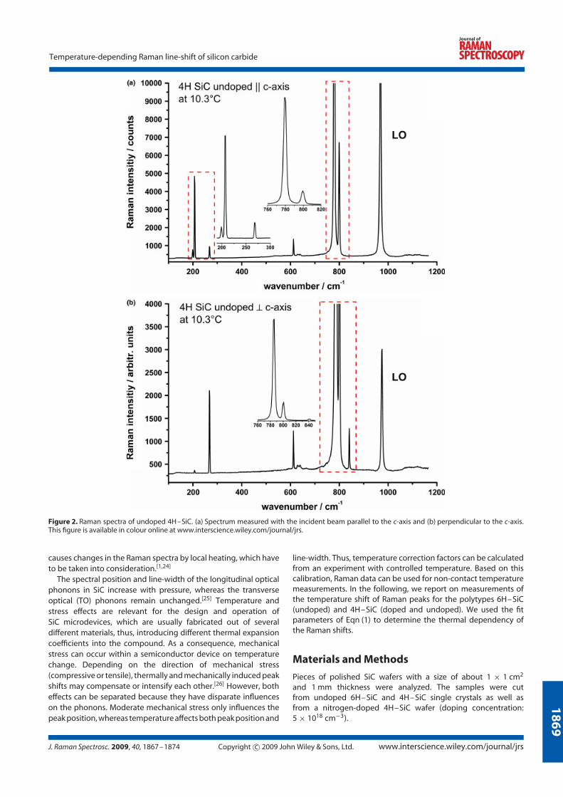
18
69
Temperature-depending Raman line-shift of silicon carbide
Figure 2. Raman spectra of undoped 4H–SiC. (a) Spectrum measured with the incident beam parallel to the c-axis and (b) perpendicular to the c-axis.This figure is available in colour online at www.interscience.wiley.com/journal/jrs.
causes changes in the Raman spectra by local heating, which haveto be taken into consideration.[1,24]
The spectral position and line-width of the longitudinal opticalphonons in SiC increase with pressure, whereas the transverseoptical (TO) phonons remain unchanged.[25] Temperature andstress effects are relevant for the design and operation ofSiC microdevices, which are usually fabricated out of severaldifferent materials, thus, introducing different thermal expansioncoefficients into the compound. As a consequence, mechanicalstress can occur within a semiconductor device on temperaturechange. Depending on the direction of mechanical stress(compressive or tensile), thermally and mechanically induced peakshifts may compensate or intensify each other.[26] However, botheffects can be separated because they have disparate influenceson the phonons. Moderate mechanical stress only influences thepeak position, whereas temperature affects both peak position and
line-width. Thus, temperature correction factors can be calculatedfrom an experiment with controlled temperature. Based on thiscalibration, Raman data can be used for non-contact temperaturemeasurements. In the following, we report on measurements ofthe temperature shift of Raman peaks for the polytypes 6H–SiC(undoped) and 4H–SiC (doped and undoped). We used the fitparameters of Eqn (1) to determine the thermal dependency ofthe Raman shifts.
Materials and Methods
Pieces of polished SiC wafers with a size of about 1 × 1 cm2
and 1 mm thickness were analyzed. The samples were cutfrom undoped 6H–SiC and 4H–SiC single crystals as well asfrom a nitrogen-doped 4H–SiC wafer (doping concentration:5 × 1018 cm−3).
J. Raman Spectrosc. 2009, 40, 1867–1874 Copyright c© 2009 John Wiley & Sons, Ltd. www.interscience.wiley.com/journal/jrs
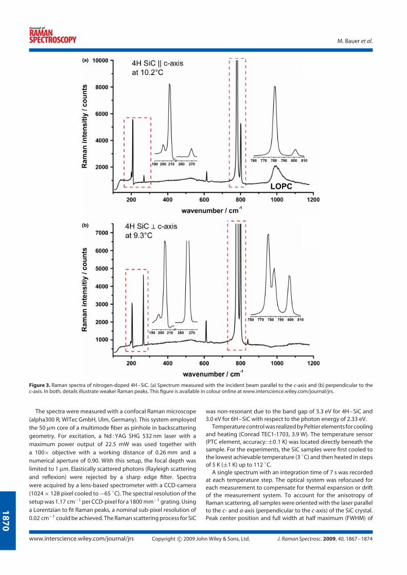
18
70
M. Bauer et al.
Figure 3. Raman spectra of nitrogen-doped 4H–SiC. (a) Spectrum measured with the incident beam parallel to the c-axis and (b) perpendicular to thec-axis. In both, details illustrate weaker Raman peaks. This figure is available in colour online at www.interscience.wiley.com/journal/jrs.
The spectra were measured with a confocal Raman microscope(alpha300 R; WITec GmbH, Ulm, Germany). This system employedthe 50 µm core of a multimode fiber as pinhole in backscatteringgeometry. For excitation, a Nd : YAG SHG 532 nm laser with amaximum power output of 22.5 mW was used together witha 100× objective with a working distance of 0.26 mm and anumerical aperture of 0.90. With this setup, the focal depth waslimited to 1 µm. Elastically scattered photons (Rayleigh scatteringand reflexion) were rejected by a sharp edge filter. Spectrawere acquired by a lens-based spectrometer with a CCD-camera(1024 × 128 pixel cooled to −65 C). The spectral resolution of thesetup was 1.17 cm−1 per CCD-pixel for a 1800 mm−1 grating. Usinga Lorentzian to fit Raman peaks, a nominal sub-pixel resolution of0.02 cm−1 could be achieved. The Raman scattering process for SiC
was non-resonant due to the band gap of 3.3 eV for 4H–SiC and3.0 eV for 6H–SiC with respect to the photon energy of 2.33 eV.
Temperature control was realized by Peltier elements for coolingand heating (Conrad TEC1-1703, 3.9 W). The temperature sensor(PTC element, accuracy: ±0.1 K) was located directly beneath thesample. For the experiments, the SiC samples were first cooled tothe lowest achievable temperature (3 C) and then heated in stepsof 5 K (±1 K) up to 112 C.
A single spectrum with an integration time of 7 s was recordedat each temperature step. The optical system was refocused foreach measurement to compensate for thermal expansion or driftof the measurement system. To account for the anisotropy ofRaman scattering, all samples were oriented with the laser parallelto the c- and a-axis (perpendicular to the c-axis) of the SiC crystal.Peak center position and full width at half maximum (FWHM) of
www.interscience.wiley.com/journal/jrs Copyright c© 2009 John Wiley & Sons, Ltd. J. Raman Spectrosc. 2009, 40, 1867–1874
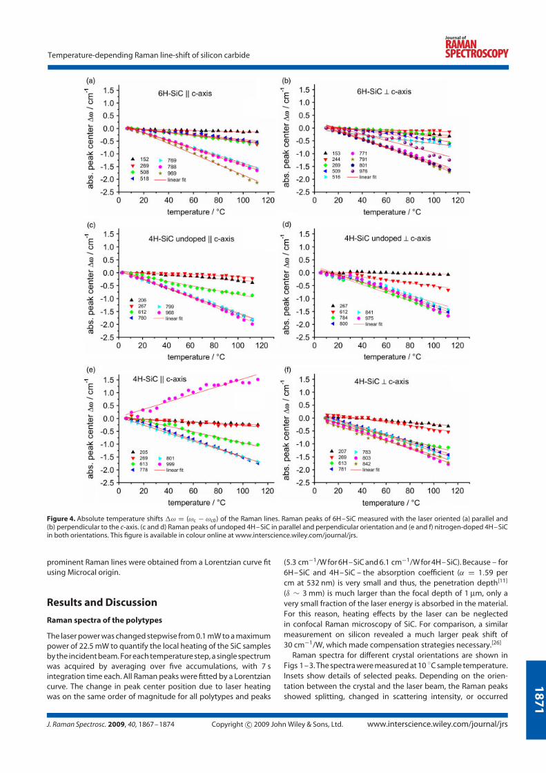
18
71
Temperature-depending Raman line-shift of silicon carbide
Figure 4. Absolute temperature shifts ω = (ωc − ωc0) of the Raman lines. Raman peaks of 6H–SiC measured with the laser oriented (a) parallel and(b) perpendicular to the c-axis. (c and d) Raman peaks of undoped 4H–SiC in parallel and perpendicular orientation and (e and f) nitrogen-doped 4H–SiCin both orientations. This figure is available in colour online at www.interscience.wiley.com/journal/jrs.
prominent Raman lines were obtained from a Lorentzian curve fitusing Microcal origin.
Results and Discussion
Raman spectra of the polytypes
The laser power was changed stepwise from 0.1 mW to a maximumpower of 22.5 mW to quantify the local heating of the SiC samplesby the incident beam. For each temperature step, a single spectrumwas acquired by averaging over five accumulations, with 7 sintegration time each. All Raman peaks were fitted by a Lorentziancurve. The change in peak center position due to laser heatingwas on the same order of magnitude for all polytypes and peaks
(5.3 cm−1/W for 6H–SiC and 6.1 cm−1/W for 4H–SiC). Because – for6H–SiC and 4H–SiC – the absorption coefficient (α = 1.59 percm at 532 nm) is very small and thus, the penetration depth[11]
(δ ∼ 3 mm) is much larger than the focal depth of 1 µm, only avery small fraction of the laser energy is absorbed in the material.For this reason, heating effects by the laser can be neglectedin confocal Raman microscopy of SiC. For comparison, a similarmeasurement on silicon revealed a much larger peak shift of30 cm−1/W, which made compensation strategies necessary.[26]
Raman spectra for different crystal orientations are shown inFigs 1–3. The spectra were measured at 10 C sample temperature.Insets show details of selected peaks. Depending on the orien-tation between the crystal and the laser beam, the Raman peaksshowed splitting, changed in scattering intensity, or occurred
J. Raman Spectrosc. 2009, 40, 1867–1874 Copyright c© 2009 John Wiley & Sons, Ltd. www.interscience.wiley.com/journal/jrs
18
72
M. Bauer et al.
Table 1. Peak center positions of the Raman peaks measured in undoped 4H–SiC and 6H–SiC and nitrogen-doped 4H–SiCa
FTA, transversal (planar) acoustic FLA, longitudinal (axial) acoustic
Polytype x = q/qb || (cm−1) ⊥ (cm−1) || (cm−1) ⊥ (cm−1)
4H undoped 0 – – – –
2/4 199.1, 207.2 E2 206.6 E2 – –
4/4 268.1 E2 268.1 E1 612.5 A1 612.2 A1
4H doped 0 – – – –
2/4 200.0, 208.1 E2 196.8, 204.6 E2 – –
4/4 269.5 E1 266.4 E2 613.9 A1 610.6 A1
6H undoped 0 – – – –
2/6 148.5, 154.2 E2 153.9 E2 – 481.8 B1
4/6 244.8 E2 239.4, 244.3 E1 508.5, 517.6 A1 509.2, 516.8 A1
6/6 270.3 E1 270.2 E2 – –
FTO, transversal (planar) optic FLO, longitudinal (axial) optic
Polytype x = q/qb || (cm−1) ⊥ (cm−1) || (cm−1) ⊥ (cm−1)
4H undoped 0 799.4 E2 800.3 E1 968.3 A1 974.6 A1
2/4 779.4 E2 785.4 E2 – –
4/4 – – – 840.9 A1
4H doped 0 801.2 E1 798.9 E1 999.2 A1 –
2/4 780.9 E2 777.5, 783.1 E2 – –
4/4 – – – 839.4 A1
6H undoped 0 800.7 E1 801.4 E1 970.4 A1 976.4 A1
2/6 792.7 E2 792.2 E2 – –
4/6 – – 893.2 A1 –
6/6 771.0 E2 770.9 E2 – –
a The assignment of the Raman peaks with phonon modes and symmetries follows Ref. [7].
exclusively in one orientation. Due to the finite angle betweenthe crystal axis and the direction of the incident photons, Ramanscattering also occurred at phonons corresponding to other crystalorientations. This explains small additional peaks in the spectra.The assignment and origin of the Raman lines are given in Table 1.
Undoped 6H–SiC
The Raman spectrum of 6H–SiC with the laser beam oriented inparallel alignment with the c-axis is shown in Fig. 1(a). Figure 1(b)shows the Raman spectrum of the same sample, measured withthe incident laser perpendicular to the c-axis. Both measurementswere acquired at about 10 C. The major peaks were nearly at thesame spectral position for both orientations. The single peak at154 cm−1 (Folded Transversal Acoustic (FTA) mode, E2 symmetry)measured for parallel orientation, however, was split into twopeaks in the spectrum recorded in perpendicular orientation. Inparallel orientation, the peaks at 240 cm−1 (split FTA mode, E1
symmetry) were not as intense as in the perpendicular orientation.For 509 cm−1 (Folded Longitudinal Acoustic (FLA), A1 symmetry)and 517 cm−1 (FLA, A1 symmetry) in the 6H–SiC spectra – presentin both orientations – an origin from Si-Si nearest neighbors couldbe assumed.[6] This effect will be discussed later. Note that theSi–Si Raman band appears at 521 cm−1 for unstressed siliconcrystals. For the folded longitudinal acoustic phonon peaks in6H–SiC, the origin was determined in the acoustic branch ofthe second-order Raman scattering as supported by theoreticalcalculations reported in literature.[6,27] The TO peak (801 cm−1)was more intense in the perpendicular orientation, whereas theLO peak (970 cm−1) was stronger in the parallel alignment.
Undoped 4H–SiC
Raman spectra were obtained for undoped 4H–SiC with theincident laser oriented parallel (Fig. 2(a)) and perpendicular(Fig. 2(b)) to the c-axis. Both spectra were recorded at about 10 Csample temperature. The peaks at 200 cm−1 (split FTA, E2) weremore intense in the parallel than in the perpendicular orientation.The peak at 268 cm−1 (FTA, E2), however, was more intense inperpendicular orientation. The FLA peak (610 cm−1), FTO peak(780 cm−1) and the LO peak (970 cm−1) showed no dependencyon orientation.
Nitrogen-doped 4H–SiC
The Raman spectrum in Fig. 3(a) was obtained for the nitrogen-doped 4H–SiC sample (approx. 5 × 1018 cm−3) with the incidentlaser oriented parallel to the c-axis. Figure 3(b) illustrates theresults for the same sample in perpendicular orientation (bothmeasurements at about 10 C). Here, the FTA peak at 200 cm−1
was similar in both spectra. The peak at 269 cm−1 (FTA, E1) wasstronger in perpendicular orientation. The folded TO peak (FTO, E2)at 781 cm−1 was split into a doublet with 777 cm−1 and 783 cm−1
in perpendicular orientation. The undoped 4H–SiC sample did notshow any splitting. In the perpendicular geometry, an additionalpeak appeared at 839 cm−1 (FLO, A1) while the LOPC line at999 cm−1 vanished. The FLO peak at 841 cm−1 – only present inperpendicular geometry – was not affected by doping. The FLOpeak showed the same appearance for the doped and undopedSiC samples.
www.interscience.wiley.com/journal/jrs Copyright c© 2009 John Wiley & Sons, Ltd. J. Raman Spectrosc. 2009, 40, 1867–1874
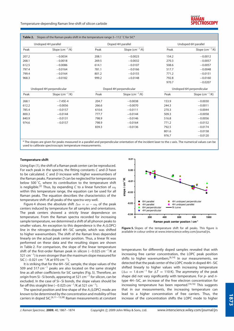
18
73
Temperature-depending Raman line-shift of silicon carbide
Table 2. Slopes of the Raman peaks shift in the temperature range 3–112 C for SiCa
Undoped 4H parallel Doped 4H parallel Undoped 6H parallel
Peak Slope (cm−1/K) Peak Slope (cm−1/K) Peak Slope (cm−1/K)
207.2 −0.0034 208.1 −0.0023 154.2 −0.0012
268.1 −0.0018 269.5 −0.0032 270.3 −0.0057
612.5 −0.0086 614.1 −0.0107 508.6 −0.0057
797.4 −0.0164 781.1 −0.0166 517.7 −0.0048
799.4 −0.0164 801.2 −0.0155 771.2 −0.0151
968.3 −0.0182 999.2 +0.0148 792.8 −0.0160
970.7 −0.0207
Undoped 4H perpendicular Doped 4H perpendicular Undoped 6H perpendicular
Peak Slope (cm−1/K) Peak Slope (cm−1/K) Peak Slope (cm−1/K)
268.1 −7.45E-4 204.7 −0.0038 153.9 −0.0030
612.2 −0.0056 266.6 −0.0070 244.3 −0.0011
785.4 −0.0157 610.6 −0.0111 270.3 −0.0044
800.3 −0.0144 777.7 −0.0144 509.3 −0.0058
840.9 −0.0131 798.9 −0.0146 516.8 −0.0056
974.6 −0.0157 798.9 −0.0164 771.2 −0.0152
839.3 −0.0136 792.5 −0.0174
801.6 −0.0158
976.7 −0.0120
a The slopes are given for peaks measured in a parallel and perpendicular orientation of the incident laser to the c-axis. The numerical values can beused to calibrate spectroscopic temperature measurements.
Temperature shift
Using Eqn (1), the shift of a Raman peak center can be reproduced.For each peak in the spectra, the fitting constants C and D haveto be calculated. C and D increase with higher wavenumbers ofthe Raman peaks. Parameter D can be neglected for temperaturesbelow 500 C, where its contribution to the temperature shiftis negligible.[2] Thus, by expanding C to a linear function of ω0
within this temperature range, the equation can be used for allRaman peaks. The equation describes the characteristics of thetemperature shift of all peaks of the spectra very well.
Figure 4 shows the absolute shift ω = ω − ω0 of the peakcenters induced by temperature for all samples and orientations.The peak centers showed a strictly linear dependence ontemperature. From the Raman spectra recorded for increasingsample temperature, we determined a shift of all phonon peaks tosmaller values. An exception to this dependence is the A1(LOPC)line in the nitrogen-doped 4H–SiC sample, which was shiftedto higher wavenumbers. The shift of the Raman lines dependedlinearly on the actual peak center position. Thus, a linear fit wasperformed on these data and the resulting slopes are shownin Table 2. For comparison, the slope of the linear temperatureshift of the first-order Raman peak in silicon (−0.025 cm−1/K at521 cm−1) is even stronger than the maximum slope measured forSiC (−0.021 cm−1/K at 970 cm−1).
It is striking that for the 6H–SiC sample, the slope values of the509 and 517 cm−1 peaks are also located on the same straightline as all other coefficients for SiC samples (Fig. 5). Therefore, anorigin from Si–Si bonds, appearing at 521 cm−1 for silicon, can beexcluded. In the case of Si–Si bonds, the slope values should befar off this straight line (−0.025 cm−1/K at 521 cm−1).
The spectral position and line-shape of the A1(LOPC) mode areknown to be determined by the concentration and mobility of freecarriers in doped SiC.[6,11 – 13,28] Raman measurements at constant
Figure 5. Slopes of the temperature shift for all peaks. This figure isavailable in colour online at www.interscience.wiley.com/journal/jrs.
temperatures for differently doped samples revealed that withincreasing free carrier concentration, the LOPC peak positionshifts to higher wavenumbers.[6,14] In our measurements, wedetected that the peak center of the LOPC mode in doped 4H–SiCshifted linearly to higher values with increasing temperature(ω = 1.6 cm−1 for T = 110 K). The asymmetry of the peakshape did not vary significantly with temperature. For p- and n-type 4H–SiC, an increase of the free electron concentration forincreasing temperature has been reported.[14,16] This suggeststhat in our measurements, the increasing temperature canlead to a higher concentration of free carriers. Thus, theincrease of the concentration shifts the LOPC mode to higher
J. Raman Spectrosc. 2009, 40, 1867–1874 Copyright c© 2009 John Wiley & Sons, Ltd. www.interscience.wiley.com/journal/jrs
18
74
M. Bauer et al.
wavenumbers, overcompensating the temperature-induced shiftto lower wavenumbers.
Focusing on the position of the Raman peak center (ω0) withinthe spectra and the corresponding slope of the temperature shift,the slope is increasing with higher peak center position. This curveshows a nearly linear behavior as well (illustrated in Fig. 5). Theenergy transfer during the inelastic scattering increases. Fromour data, we derive the coefficient for the temperature-inducedline-shift: C(ω0) = −2.188 × 10⁻⁵ ω0 + 0.002 cm−1.
Conclusion
The peak positions of the Raman lines in SiC change with varyingtemperature. We have investigated their temperature dependencein the range from 3 to 112 C. We observed a linear relationbetween line-shift and temperature. The slope of the temperatureshift increases with increased energy transfer due to inelasticscattering showing a linear dependency with temperature in thetemperature range of aboutT = 110 K. Although the peak centerposition is typically shifted to lower wavenumbers with increasingtemperature, the nitrogen-doped plasmon-coupled longitudinaloptical phonon mode (LOPC) showed a contrary behavior, movingto higher values.
For accurate stress and temperature measurements in SiCdevices, the linearity of the temperature shift within the typicaloperation temperatures simplifies spectroscopic temperaturemeasurements. We found that, in contrast to silicon, the effect oflocal heating by the laser at 532 nm wavelength can be neglectedin confocal Raman spectroscopy due to the small absorptioncoefficient of SiC. Our results provide calibration data for spectraltemperature measurements in SiC that simplify the spectroscopiccharacterization of electrical properties, mechanical stress andlocal temperatures.
Acknowledgements
We thank the Deutsche Forschungsgemeinschaft (DFG) cluster ofexcellence ‘Nanosystems Initiative Munich’ for financial support.
References
[1] T. Beechem, S. Graham, S. P. Kearney, L. M. Phinney, J. R. Serrano,Rev. Sci. Instrum. 2007, 78.
[2] H. Harima, T. Hosoda, S. Nakashima, J. Electron. Mater. 1999, 28,141.
[3] K. Dombrowski, Micro-Raman investigation of mechanical stress in Sidevice structures and phonons in SiGe, Dissertation thesis, TU-Cottbus(Cottbus), 2000.
[4] D. W. Feldman, J. H. Parker, W. J. Choyke, L. Patrick, Phys. Rev. 1968,173, 787.
[5] D. W. Feldman, J. H. Parker, W. J. Choyke, L. Patrick, Phys. Rev. 1968,170, 698.
[6] J. C. Burton, L. Sun, M. Pophristic, S. J. Lukacs, F. H. Long, Z. C. Feng,I. T. Ferguson, J. Appl. Phys. 1998, 84, 6268.
[7] S. Nakashima, H. Harima, Phys. Stat. Sol. A 1997, 162, 39.[8] J. C. Burton, L. Sun, F. H. Long, Z. C. Feng, I. T. Ferguson, Phys. Rev. B
1999, 59, 7282.[9] M. V. Klein, P. J. Colwell, B. N. Ganguly, Phys. Rev. B 1972, 6,
2380.[10] M. Roschke, F. Schwierz, IEEE T. Electron. Dev. 2001, 48, 1442.[11] H. Harima, Microelectron. Eng. 2006, 83, 126.[12] S. Nakashima, H. Harima, J. Appl. Phys. 2004, 95, 3541.[13] S. Nakashima, T. Mitani, J. Senzaki, H. Okumura, T. Yamamoto,
J. Appl. Phys. 2005, 97.[14] M. Laube, F. Schmid, G. Pensl, G. Wagner, M. Linnarsson, M. Maier,
J. Appl. Phys. 2002, 92, 549.[15] A. Compaan, H. J. Trodahl, Phys. Rev. B 1984, 29, 793.[16] D. Olego, M. Cardona, Phys. Rev. B 1982, 25, 3889.[17] D. G. Mead, G. R. Wilkinson, J. Raman Spectrosc. 1977, 6, 123.[18] Z. Li, R. C. Bradt, J. Mater. Sci. 1986, 21, 4366.[19] Z. Li, R. C. Bradt, J. Am. Ceram. Soc. 1987, 70, 445.[20] C. Ulrich, A. Debernardi, E. Anastassakis, K. Syassen, M. Cardona,
Phys. Stat. Sol. B 1999, 211, 293.[21] J. Menendez, M. Cardona, Phys. Rev. B 1984, 29, 2051.[22] T. R. Hart, R. L. Aggarwal, B. Lax, Phys. Rev. B 1970, 1, 638.[23] R. Tsu, J. G. Hernandez, Appl. Phys. Lett. 1982, 41, 1016.[24] S. Kouteva-Arguirova, T. Arguirov, D. Wolfframm, J. Reif, J.Appl.Phys.
2003, 94, 4946.[25] A. Debernardi, C. Ulrich, K. Syassen, M. Cardona, Phys. Rev. B 1999,
59, 6774.[26] M. Bauer, A. M. Gigler, C. Richter, R. W. Stark, Microelectron. Eng.
2008, 85, 1443.[27] W. Windl, K. Karch, P. Pavone, O. Schutt, D. Strauch, W. H. Weber,
K. C. Hass, L. Rimai, Phys. Rev. B 1994, 49, 8764.[28] H. Harima, S. Nakashima, T. Uemura, J. Appl. Phys. 1995, 78, 1996.
www.interscience.wiley.com/journal/jrs Copyright c© 2009 John Wiley & Sons, Ltd. J. Raman Spectrosc. 2009, 40, 1867–1874
Optics Express 71
7.3 Nanoscale residual stress-field mapping
around nanoindents in SiC by IR s-SNOM
and confocal Raman microscopy
Alexander M. Gigler, Andreas J. Huber, Michael Bauer, Alexander Ziegler,
Rainer Hillenbrand and Robert W. Stark
Optics Express, Vol. 17, Issue 25, pp. 22351 - 22357
Permanent weblink:
http://dx.doi.org/10.1364/OE.17.022351

72 Optics Express
! " #$% ! & '( ! )& $% ! * + , !-./012345064.78.9234:.26;.96<=37650642>.?@[email protected];E=FGH2I=5=>=26AGJ6=<03A=4K4.HL6@:06B.M:030A=06A43N.O-B.PQRRR.HD6=@:[email protected]>=;03B.UQQ-P./767A4=2.Z.?26.?0W2A4=26B.?12=6.R.X06403.873.V267?@=06@0.[X0V?\B.?@:0>>=6FA43N.OB.PQ] .HD6=@:B.S03526T.O.H7>0_D>230.?43D_4D3W=7>7F=0B.H2IG>26@_GY6A=4D4.8L3.a=7@:05=0B.PU-bU.H234=6A3=0;B.S03526T.b.Yc9dae?fJ9B.a2AgD0.h7D6;24=76.873.?@[email protected]=F>03j>5DN;0. klmnlopqlplrprstrunrvltrlplwtxtysrlypztunl|t~lyzwvpxlltrzpznul|lwypvvnztrvqnlwyprrtrlrnpztnxulsqvtypxlotyzswysql|wlprulysrsypxlpoprlotyzswysqlprultrvnzqznvlvnlznwxvtrltopnwltrlvnzowlslxsypxlznwtupxlwvznwwtnxuwllysoqpztrlrnpztnxullprulysrsypxlpoprltopnwlnltrulvpvlvnlwvznwwtruynulwtvwlslvnlxsrtvutrpxlsqvtypxlqsrsrznnrytnwl|lprulvnlznxpvnulwtvlslvnlqsrsrqsxpztvsrlrnpztnxulznwsrprynltnlztwnlvslpoprlprulwltopnlysrvzpwvwlznwqnyvtnxlmnlpqqxlwtrxnznnryllwlszlrprswypxnlznwsxnultoptrlslxsypxlwvznwwtnxuwlprulysrsypxlpoprlotyzswysqlvslsvptrlvnlysoqxnvnlwqnyvzpxltrszopvtsrlpsvlwvznwwtruynulwtvwlslvnlqsrsrlznnrytnwlpvlutzpyvtsrlxtotvnulwqpvtpxlznwsxvtsrlnlwqpvtpxlnvnrwtsrlslvnlxsypxlwvznwwtnxulpzsrulvnlrprstrunrvlpznnwlnxxlnvnnrlsvlvnyrtnwlzlznwxvwlunosrwvzpvnlvpvlsvlonvsuwltunpxxlysoqxnonrvlnpylsvnzlpxxstrlszlvnlunvptxnulprpxwtwlslwvznwwtnxuwlpvlnlopvnztpxlprulzptrlsrupztnwltrltyzsxnyvzsnyprtypxwvnowl|lszltrlnrtrnnznulrprswvzyvznwllqvtypxlsytnvlslonztyplkl|lnpztnxulotyzswysql| lpoprlotyzswysql| ltrnpzlprulrsrxtrnpzlxtvlwypvvnztrlzsolwzpynwl|l¡sxpztvsrwl| lzpynlqxpwosrwl| lqnyvzswysqltrnxpwvtylwypvvnztrltryxutrlpoprl,l¢l¡nvnzll¢pxonzl£l¤ztrwllnyrnzllzynzll¥pxsnzlll¥txnzllmlvpz¦lprulmlnrwyl§npwznonrvlslvnlnyprtypxlvptxtvlslnotysruyvszltrnlvzyvznwltrlnxnprvlnutpl~lzprwl©lªl|lllnt«nwvrtlprul¬l¥ztuytrl§nlwnlslwvznwwnulwtxtysrltrllvzprwtwvszwlprul~lwvzyvznwlwwltyzsnxnyvzsrl!|l®ª l|ll lpxtpl?=>[email protected]=;0.7E03./0<=@0Al|mszxulytnrvttyltrpqsznlll£l£pztopll£swsuplprullp¦pwtopl§noqnzpvznlonpwznonrvltrlplwtxtysrlypztunlxtvlnotvvtrlutsunllpoprlwypvvnztrllxnyvzsrlpvnzl%|lªl|llllmtx¦trwsrl¥lnpunrlprul¢ll¢trxnl§£tznwsxvtsrlnxpwvtylwvzptrlonpwznonrvlzsolnxnyvzsrlpy¦wypvvnzlutzpyvtsrlqpvvnzrw°lrnlxnnxwlslwnrwtvttvl±xvzpotyzswysql²©|l®ªl| l lllmtx¦trwsrl¥lnpunrlprul¢ll¢trxnl§pqqtrlwvzptrwlpvlvnlrprswypxnlwtrlnxnyvzsrlpy¦lwypvvnzlutzpyvtsrlqnzxpvvtynwltyzswvzyvl&*|lªl|l®llpnzlll¥txnzlll£nzll£txxnrzprulprullmlvpz¦l§noqnzpvznlunqnrutrlpoprlxtrnwtvltrlwtxtysrlypztunllpoprlqnyvzswyl|vslnlqxtwnulust°³zwlllpnzlll¥txnzl~ltyvnzlprullmlvpz¦l§¬twpxt«trlwvznwwltrlwtxtysrlotyzslyprvtxnnzwlwtrlwyprrtrlysrsypxlpoprlwqnyvzswysqltyzsnxnyvzsrlrl*| lª l|lllnnynoll¥zppoll¡l¤npzrnlll¡trrnlprulllnzzprsl§rtvnulzvtyxn°ltoxvprnswlopqqtrlslvnoqnzpvznlprulwvznwwltrlotyzsuntynwlwtrlotyzspoprlwqnyvzswysqlnlytlrwvzolµ| l l|®l¶··¹º¹»¼»½·¾¿ÀÀ»ÁÂà ÄÅÆÅÇÈÅÉ»·Ê»ÂÅË»ÌÀÀÍλÏÅÈÇÐÅÉ»ÌÑ»ÒÆÓ»ÌÀÀÍλÔÆÆÅËÓÅɻͻÕÖÈ»ÌÀÀÍλË×ØÙÇÐÚÅɻ̺»ÕÖÈ»ÌÀÀÍÛÜÝÞßààáÞâãä åÞæçèçéêçëÞßààáÞìÞíîïðÞñåòÞÞóîðÞßôÞìÞâõö÷ÜãÞøùõúøããÞÞßßûôñ
!"#$%&'()* +,+- +++(.+/*012342506786 #7 9 77 "5 :(* - )(/;*/39 <=!# $ 7 > !?1 @7 "#$%'A(*),,B-),+ (...* %4C0$1 2D4 EF2GEE EGG 7 % 5 H 56179#%65 "5 $G:(,*,; -,;,(/.*B2%G!!2G6 10GF1 I1! J !> 9#$ 7 #"23#K:(*)/)+-)/, (..+*;!5 6 7 00 7 $ 7 !##"#! !3LM&(* .-)B(..,*)=J !5 6 7 7 # !179#$ 7 9 J 7"23#M'(,*/;+ -/;.(.+.*,I4$ 7 ## 7 "!7!LL(/* .-;B(..)*+!0!$ 97!#"23#NO()*$; -$+(..*.%= 70H9G#96I= 7$!4 72% 9 2G6> J$ 7 J79 J!PH "3#GKQ(/B*; ;-; ,(/ */2G E= $ 7 7)0## 9 ?37 > 7"#$GN&(/)*B;-B+(..B*/2G E= $ 7 7)0## 9 $#"#$GNN))(..)*//GH R 30 G5# $ 7 # 9 9"2$ 7 !:O(*B/-B/)(/.*/ 30 2!SJD!D G5#0 $ 7 7#> 9 9"#$GAO(.*.;; (/ */B 6H %G $5 7 6 2$ 7 7? $ 7 9 7 "2$ 7 !:O( */B-/B (/.*/;6H 1 6 7# ?# #"G 7&'(*) /-) B(/.*/)6H % 6 #7 #$ 7 7 "2%L(;* ,,- +.(/+*/,50 # J > E! 0I93I7 7 != > J J # # 9# $ 7 # 7#"2$ 7 !QK()*)+B-).)(/,*/+3 50 # J > != > 0# $ 7 # 7# "$!I7NA(* ,)(/+*/.1=7 $09 5 7#9# 7 " $!G3QM&(+,*,+,-+;(/B* $09 9 1=7 7 7 "5 :LK()+.B*;.-)/(//* !=9 082!!H T7G!4! 073# 7# "#$GLOO(/;*/;)B (/+* /3095 9 $09 5 9# 7"5 GM(B*,,B-,,+(/)* 5 $09 !9> 9#9 77 "5 Q(.*))-).(/B* B32093F=T6 $09 I # 7"5 5 :( *; -;,(/.* ;5309 $09 #9 6 #"3#GKA(*/B(/)* )<!74I9 2=4 0$ 7 7 3 #U 7 7"9!:&(*. -.,(/)* ,47% ! $! 6 $ 7 #7 7#77# #7 # "3 ''(B*B);,-B));(/,* +HC $% 6 "237 7!AO( *), -)+(/,* .%60!! 0!6H @ # 9#7$ 7 #"23#LOL()*) ; (/,*VWWXYZY[\[]W_ [abc defeghei[Wj[bek[l mn[oehgpei[lq[rfs[l mn[tffeksei[m[uvh[l mn[kwxygpzei[lZ[uvh[l m|~~ ~~~~~~~~~~|~~~
!" # $ $ % &'(!) $* $* + + , % &-(!. + + /0)1!2 $ $ &3$4(!5$ ,+ !" $ + % 6 6 !7 + $ # $ + +8 &9$:(!" $* $ + + 6 !; 6 # &<='3($+ % > * 6 !> 0) /?;$5;1/?.$5.1 !0 0) , &'4$'9(!5 # * , $ > &':(!5 * $ ,+ &'<$'@(% &'A(!> 6 $! ! !5 + + 6+ + * &A(!B 8* $* 8 ++ $ + !C* $ &-D$-'(* *&'<(!2 $ # + $ $ == !2 0)$* $ + # $+ + 0)/'!9A 93-1 +-&<(!C $> + + 0) * + , !) 6 +!5 + + % 6 !" # $% > +%* &--=-@(!; 6 % % /%0E.1&-A(!; 6 $%0E.+ % 0)$0E$0.$FE$F;* !2%0E. , ;" /;"1 + !5 # # , %/ +1$ % 6 G ?. 6 &3D$3'(!; 6 $ +8 *% &3-($6&33($&3'(!5 % % 0) * $* + % &34(!C $* > % :C%0) + !H % 5.?. !2* %0E. !.*>%0E.+ !IJJKLMLNONPJQRSSNTUV WXYXZ[X\NJ]NUXN_SSaNbX[ZcX\N_dNeYfN_SSaNgYYXfX\NNhi[N_SSaNjklZcmX\N_MNhi[N_SSnopqrsstquvw xqyzz|z~qrsstqqqxqqqrqquovqvvqqrr
! " " #$%&'()*+',-%'./%0)(12/-%3 45678 5674999:8 ; 567 4999:8 7 5994 <8" 4=8 9>? > >9 :@9 4 8 ! ! !4 @99!A3BC6D C 8 "6CEFGC 4>@HHH>38 I J 3:K99L: ::ML:77; !<N 9O;@9P567 H@@PG:99QJ49H5G9R98; N 6S NT N O99G >9U :U 48 4G8 V@9@HW@>XB NG " 7H YB!ZKKML:YB!Z:9K>L:4[B!ZRH:UW::HMU8 \$%])-,(%'./%/+-_--+2.%!7 567 V:>XEH@O5L:4 G 8HO99L:4G 8>9>>L:4<G 8MKMRL:4 8MRK9L:4 8KKR@L:4 8RM:>L:4< 8B 4YZKKR@L:Y<ZRM:>L:8:!567 4YZMM>L:WRR9L:8 < 3 B <PVH9H:X a:Cb aHL:cddefgfhihjdklmmhnop qrsrturvhdwhorxhymmzh|rutrvhy~hshymmzhssrxrvhzhuhymmzhxtrvhyghuhymmz ¡¢£¤¥¦¢§¥¡©
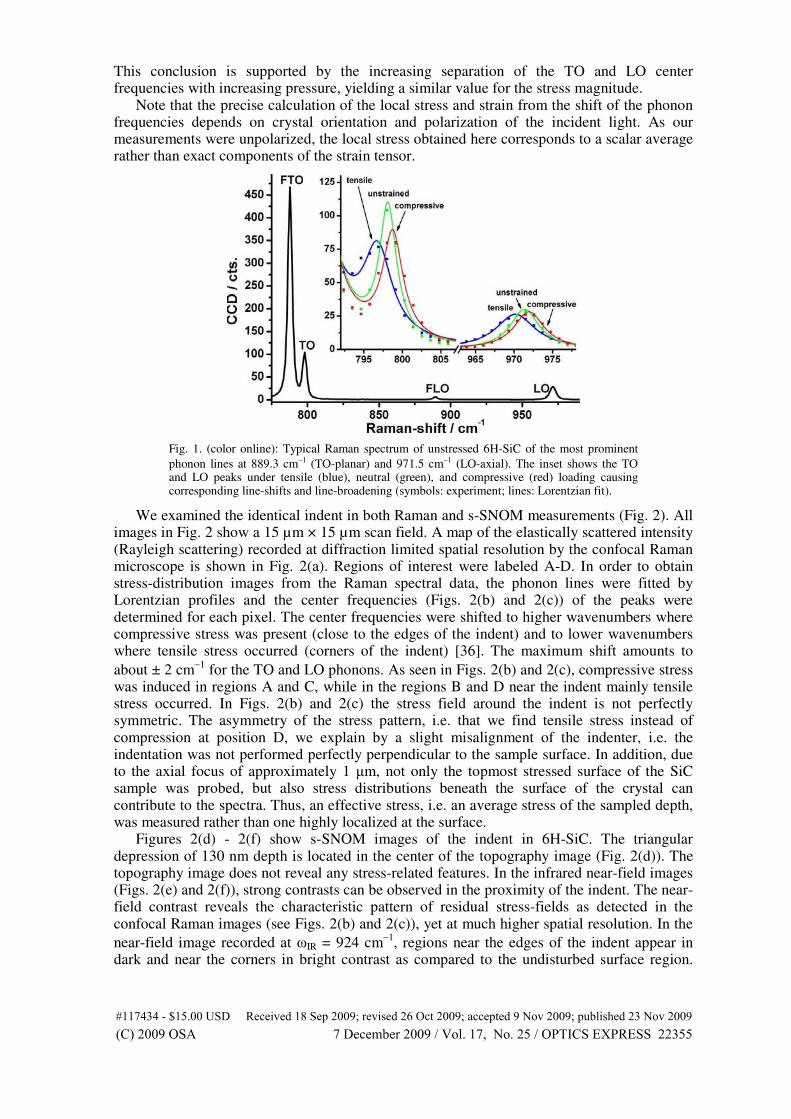
!" #$% &'()* ++,-.!"(#,/!0.!"(# 1 " # " # " # ( ( "$ 2 $ #3 %()4 " 5# 5!067!06 "% # % 5"#% (89 ( % " 5"#5"## 1 " # " #:-&; <5.! 5"#5"# * =8 9 5"#5"# 8 9 !> )* 5"#(5"#()4 &'()* !-? " 5"## ( 9 ( " 5" #5"## ( ( % " 5"#5"## 9 ( @9%A,5B.! 1 CDDEFGFHIHJDKLMMHNOP QRSRTURVHDWHORXHYMMZ[H\RUT]RVHYH_SHYMMZ[HaSSRXRVHZHbcUHYMMZ[HXdefT]gRVHYGHbcUHYMMZhijklmmnkopq rkstutvwtxklmmnkykz|k~rkkklkykoipkppkkll
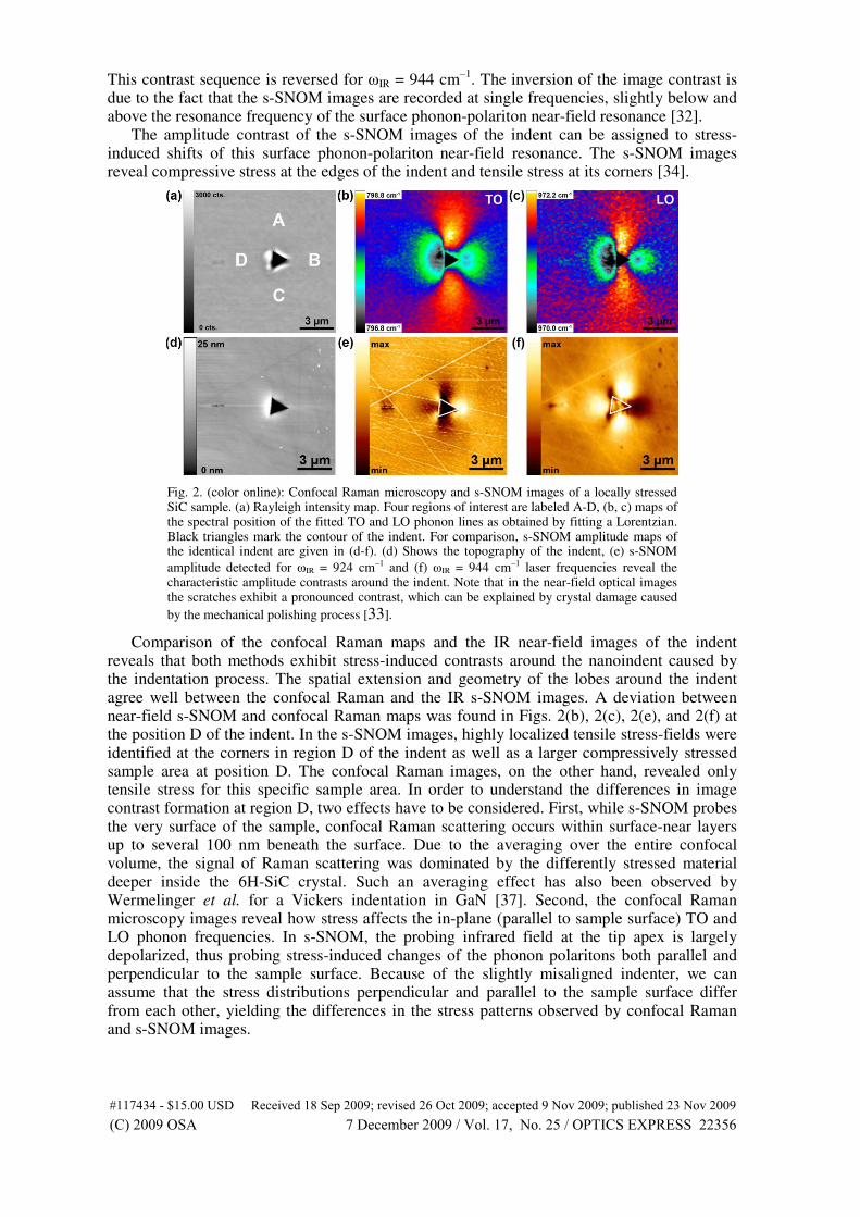
! "!!#$!%$ # &&!!'()*&! $ &&!! !&!'(*+),!!-./!&# !!!#/&!,-#!#&+ !$!01",$"-&&!&2&!$$#234!5!5 +&" &! &!,-,-%&&#",- &! ),-! !&! !&!6$& "%$6&!$##! $#!&!&'((*/&!&!!$6$ $#&&!6#!$ %!!$%! 0$%! !&% +),$-"),-"),-"),-&1 "!#!!3!!%1%!!!&!#&!&1!""!!#!&&! 1"%$+"%! &$# &!"! % !# &!77$ 1 !! "!%$#!#!&89/#! !$$$#:!;<=>?@A5B'(C*"!&#!%&!,&!!!&! -2& "&$!&&6!!#&!3" &$ &&!$&!!!&& !&! 4 !!#!"% $ && !&!!!&! "#!&$$#! DEEFGHGIJIKELMNNIOPQ RSTSUVSWIEXIPSYIZNN[\I]SVUSWIZ_ITaIZNN[\IbTTSYaSWI[IcdVIZNN[\IYefgUhSWIZHIcdVIZNN[ijklmnnolpqr sltuvuwxuylmnnolzl|~lsll|~lmlzlpjqlqqllmm
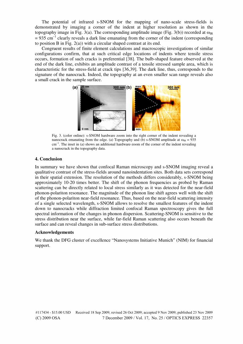
!"#$%&'( ) *+ , (- -)./0 ( )-1 - ).2-$0 )-- )! -(() 3 4 () !"#$%&' 4 () 56789:;<=>?9:7!(" (@( * 1 -1'A+A@ " - (-( ) "( ( - " ( B;C:9D<EFGEHE:I>7J)KL1M!(N!OPPQRSRTUTVPWXYYTZ[\ ]_ abTPcT[dTeYYfgThaibTejTk_lTeYYfgTm__dlbTfTnoaTeYYfgTdpqrisbTeSTnoaTeYYftuvwxyyzw| ~wwxyyzwww~wwwxwwu|w||wwxx~

80 Optics Express
Optics Express 81
7.4 Exterior surface damage of calcium fluoride
out coupling mirrors for DUV lasers
Michael Bauer, Martin Bischoff, Sigrid Jukresch, Thomas Hulsenbusch, Ansgar
Matern, Andreas Gortler, Robert W. Stark and Ute Kaiser
Optics Express, Vol. 17, Issue 10, pp. 8253 - 8263
Permanent weblink:
http://dx.doi.org/10.1364/OE.17.008253
The supporting media file may be found under the address:
http://www.opticsinfobase.org/oe/viewmedia.cfm?URI=oe-17-10-8253-1

82 Optics Express
!"#$%% &'($)* % +,-. /.0123425678569:38;<=23<26>129;?6:3@6A2B:54C2346876D:54E6:3@6D3F=583C234:G6;<=23<2HI6JK@L=MNO:P=C=G=:3HNQ3=F25H=4R46OS3<E23I6TE252H=23H45U6V0I6WXYYY6OK3=<EI6Z25C:3[6\18E252346ZC]I6_=2GH4:44H45:26Y\I6W0Yab6OK3=<EI6Z25C:3[6Yc5=2@5=<EN6;<E=GG25NQ3=F25H=4R4I6d3H4=4K426876eBBG=2@6fE[H=<HI6O:PNg=23NfG:4h60I6XaaVY6i23:I6Z25C:3[6V12345:G6c:<=G=4[6876DG2<45836O=<58H<8B[I6DG2<45836O=<58H<8B[6Z58KB6876O:425=:GH6;<=23<2I6Q3=F25H=4[6876QGCI6eG]254ND=3H42=3NeGG22600I6WbXjb6QGCI6Z25C:3[6k62C:=Gl6C=<E:2GU]:K25mG5hUK3=NCK23<E23U@26%$nopqrqstouvouwxyzqozurwu|t|xo~toxuoqtoyq~yqxyu|ot~ztotyqyyxoq|~oyryxo~qyyxoqzyrovuy~toqoyozurru|ot~ovuo~ttwooqtouwxyzotzqtoyxouoqotouoxt|~t|zouvozuuozt|xtovurqxyu|oqozurwqt~oxuouxtoouwxyzqorqxtyqottototwuxou|oxtotxtyuo~qrqstouvoqoouwxyzo~toxuoq~yqxyu|oyxoysowtt|tso~t|yxytoorzrovuroq|ooqtoxozoysot|tso~t|yxyto~qrqstouzzou|oxtotxt|qotu|qxuoy~toto~qrqstoyost|tqxt~ooqowqxyqoqxtqxyu|ouvoxtoqoxqxtoxuozxqy|toqozqzyxtoto~tzurwuyxyu|ouvoqoyorqy|o~yt|oowuxuztryzqowuzttoy|oxtowtt|ztouvoqxtoqwuoyzoqtoy|~zt~ooxtoqtoysxoq|~oxtottqxt~oxtrwtqxtoyxy|oxtotqrowuvytoowxyzqouzytxouvortyzqoo, no ¡o¢qto~qrqst£o¡¡o¤yu£o ¡ o¥zyrtoqt£o¦§oxqyutxotxtrto( ooowvto¥oo¥|trqopo¤yqro©o¢oryxoq|~o¤oo©ttoª¥vvtzxouvoqytoqtoq|~ovqztoruux|tou|o «wo ¦¡o¬roqto~qrqstouvoozuqxy|sou|osqªoy|o®owtzo°o«o §§owo««ooo¢ytrq|o¤ouxzy~oooot~qztoooxxquoo±t|ytoo²o³qxtoq|~ooq|o°tyoª¥zyrtqty|~zt~o~tsq~qxyu|ouvovt~oyyzqoq|~ozqzyrovuy~tovuo |royxusqwyzoqwwyzqxyu|ªowxo¢txxo.o«¦o oo®o¢o³uy|so¤opoywoq|~o±optoª¢qt|~zt~ovqztopqrqstªowwowxoo¦«¦¦o §o¡ootysoottoo±qxxuoq|~o®o²qytoªwxyzo~ttuwrt|xoy|oxtooouvxoqowtzxqotsyu|ªo®zo|xro¤txu~o°otoo.o« «¦oo«o©ot|opoyxqoorq||ooµqz¶tooytzo®o²qytoopwqtoowto²o¤q||ooo¢qxoo³t|yx¶yoo¥txoozywwtoq|~oottoª°uwtxytouvovuy~topotzyrtoqtouwxyz·oy|vt|ztouvoxto|rtouvo~yttzxyzoqtªo°uzo°¥o¹o««oo¦o¤o¤qyoo¢uzqxtyo¤ouuoo°o©qto¤o¥ouwytopo±q¶tqo¢o®qu|opo®xqtyo¥ot|qxoo±qxxuo®o²qyto¢o±yq||tyoo±|xtopoyxqo¤o©o°uutoq|~ooqtqyryoªovttottzxu|oqtouzyqxuoq|~oqwwyzqxyu|oy|orqxtyqozyt|ztªovoto¢txxoo«¦§oo§opoyxqo©ot|oo³uzoopwqto¥o¤qtxxyopoqzuo±o²yyqy~yoo°tyuo¥oºt|toq|~oooyu|quoªuwxyzqoq|~oryzuxzxqowuwtxytouvo¤szuqxy|so~twuyxt~oo³oq|~o°powuzttªo°uzo°¥o»o¡¦¡¡«o oooooqo¤oopt¼|tqoo¢o¤qytoq|~oo©q|soª¥xt|~t~oyvtxyrtotzyrtoqtouwxyzªoo°qxt|xo§¡¡o§ooooqvqzoo¢qtoq|~o©oµq|so²ty|oª¤txu~oq|~oqwwqqxovuoxqyy¶y|souwxyzqo~yttzxyzozuqxy|sªoo°qxt|xo«§o«o oo¢ytrq|ooo°qrqzzyopoq~o¤ouxzy~oq|~oo±t|ytoªu|xut~ou|xqry|qxyu|ox~ytoy|o |rorrtyu|o¢yxusqwªo°uzo°¥o½»½.o ¡¾ «o«o¿ÀÁÂÃÀÄÅÆÅÇÀÄÈÁÁÅÉÊË ÌÍÎÍÏÐÍÑÅÄÅÒÓÔÅÕÁÁÖ×ÅÔÍÐÏØÍÑÅÙÅÚÛÔÅÕÁÁÖ×ÅÓÎÎÍÛÜÍÑÅÀÁÅÚÛÔÅÕÁÁÖ×ÅÛÝÞßÏØàÍÑÅáÁÅÚÛÔÅÕÁÁÖâãäåæççèåéêë ììåíîïåæççèåðåñòóôåìõöåå÷òôåìçåðåéøùúãêåûüøýûêêååþæÿ
!"#$%&'(&)*&+&+,*,-$)./.01232&2435,6647,!89:;; #$8**9<8 *+,*=%9 99$)>>>063?&6435''?7(!":;8"8; #@$%&9*=A=9*%%+!$:8)8 !0B>(4C&(2,5,66,73= 8DE; 8@!:;$9*=F99$)>GHI143&4,C5,66674 8$9*9*%J!#$!KB,2'&,2345,66672$%J!#$9 B,C'&,'45'''7C!!9*$*)*%&% 8 $!99-9>K((3&(45'',7? =!"#$F&&8***8J&*8&%**%$:& I004'&C5'''7'@;D&*:;$)#%*98%8#*$-9%>L463&435''C7,6D@!8 D@$9*%*'(& 9%#9<8$)>GHI,3,&,3'5,6667,;D@&*$=&#%**$)I/K03,2&3('5''27,,";$8*<8 &%#8*& 9+,% E %9 $ >>(?('&(?3?5''?7,( 99+ !% 8M8!89$%8 %+,*$!KG2?&2??5,667,3+&D8!89M8$8%%%*&&98*8%*'($!99-9>G4?43&4?235,6667,48!""! $E*%88%&*9$!99-9>/??(&??'5''?7,2:)!)% $9* )% 5! ):7$5:)8*!#)8% 7#9JAA%N9AA,CM@OPQRSRTUVWXSYSPWSPUWZ[\]S_W[T\Raba[cWaQWdSR\eWfS\TR]S_b %9 &!* 5!"9 =@%''47!"=**,99,'&(6,,?:DD8@8**& 8! +E!"g D"h:;$%*-9!+F$ijOOWOP\TRPS\]aPS_WcY[ab]kYWaPWlSbWm_anWSPUWoeTY]S_WpSbTRbWqWr]seWtanTRWpSbTRbWuvvw,66?7xKyxz|~|~x 8 *98 %*9998&C8*8*=%99*%#*8998%9 % ?')9898=7%8*85+,7*# F98,%99*F8**9*9%**8!8%*%9%8#9*9#=9*8%* 99*98=7#888=7# F98*99%*%9 999%8*%% 6)9%999 &%% **4C,&3)%9 99988%% 9 *#8%999 9 ¡¢££¤¢££¥¦§ ©¢£ª«¬® °±²³ ´µ¶·® °¹º»¼½¾¿º¼ ±ÀÁ«²ÃÄÀÅò²Æ®ÇÈ
! "#$%$&' #$(' )* +),-$./* #$0'12 !#$. 3$'4 #$('5 ,12 )$./6-30*7-3#$333' )8-3*7-3#3/' 12 .9: $) 30*17-3 %9:3,, 7-3 39:3#3' 7-377;/<=>?@ABCDEAFG?AHI?JCBKLIG? 12 ),-$./&3278 M* .9 $%2 5 3!N" $3)-ON8*O$P/%339:3 , "$!N" 309)09:3* )Q8$% %71,*," )/0$%!* ; $/&"" ,7 )R.03% *S ;7-3 T 2 3% UVWXYVZ[\[]VZWW[_ a bcdcefcg[Z[hij[kWWlm[jcfencg[o[pqj[kWWlm[iddcqrcg[VW[pqj[kWWlm[qstuenvcg[wW[pqj[kWWlxyz|~ |~y|
! "# $% &'( )*+&),- ! .$&/0 1*! 2 $ ."34 5 67 5,6! 584958:587":5;<! =$ $) 5,6 $77 >7989?;&;>;>98917! 5 8 58@8*A! = $ $>B&CD599!. 58 $ , EFGHIJKLMJGNOPGPQJRKJJQSOGTUVWXYZY[\W]_ZYabWC C $ 2 /$ B>*!C <>! 9>!8>*@>* 2 2@>*@>*$ $ c"1*d*1e , $= $fg@" $$ !+1g@!11g@+! $ dg@d1g@ $ $ $ "1g@9 $ 2 "1g@"!"!> 2 $ $ 1#"*; $ = $ / 8>*TUhWiYZYbWYbYjklalW = > "! =1#"* > "$!$ mnopqnrstsunrvooswxy z|~srssoos~sssoos||snossoossossoo ¡¢£¤¥ ¢¦§©ª¦«©¬®
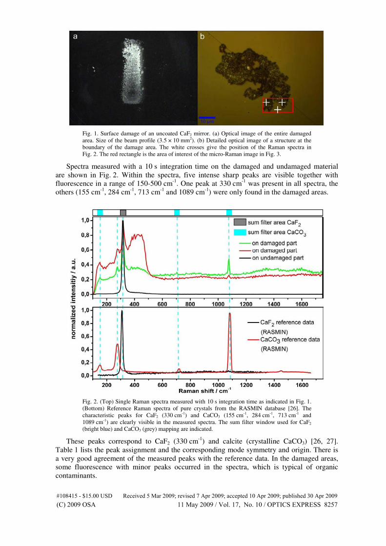
! " #$!!!%!&!# !!'&! $! !$(!)%!!*!%!$!''*'$!!!)!')+,')-' +.'$" ! #&!! $!! /&&!"!!&0123 !456#!*!' ')+,')-' +.'"%!! !#!$ $! " #!*!! ' "!45)-6#!!*!! ! !"" #!%" ! *!$ 2 !)!!$*! !)$!"!789:;8<=>=?8<@99=ABC DEFEGHEI=<=JKL=M99NO=LEHGPEI=Q=RSL=M99NO=KFFESTEI=89=RSL=M99NO=SUVWGPXEI=Y9=RSL=M99NZ[\]__]abc dd]efg]__]h]ijkl]dmn]]ojl]d_]h]apqr[b]stpusbb]]vwm
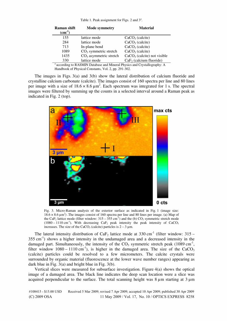
!"#$%& '()*+*!,+- '!*,.// 0 112300456 0 11230047 8 9: 1123004;5< 12=00> 11230046/ 12=00> 1123004 ?; 0 1300@@4-00 ABCD8EF D >=0 1=:>=GBH >=01 IJI::<9;> 34 34>K>@ 00@@ 0= 00@0 3004>0 L;:0: 5; :K>M5LN5LOP0>:0@K >:0K=@ @:>0@ 0 ?@ A : 0 3:4 D09A =>Q@0 0 3MG5LN5LO4>0 L;:0: 5; :34D:>103K KG/R//094 >3412=00>3;5;R;094S>0 1: =>: =112 0>M>1123004:0RO> =@ 10;093K KG/R//094>K>> = >@ 0 = >:C@ @=I> =>12=00>:3;5<09IK K;5;R;094I>> >>M>1123004:00@?K0>000=K@@ = 03@0 0>KK? @ 4:: @ 34 >@ 34J00K@@@0 ? @634>K>:0>0 0>:0 0 K0K0T@:: 0@>@0>0 >>K5O OUVWXYVZ[\[]VZWW[_ a bcdcefcg[Z[hij[kWWlm[jcfencg[o[pqj[kWWlm[iddcqrcg[VW[pqj[kWWlm[qstuenvcg[wW[pqj[kWWlxyz|~ |~y|
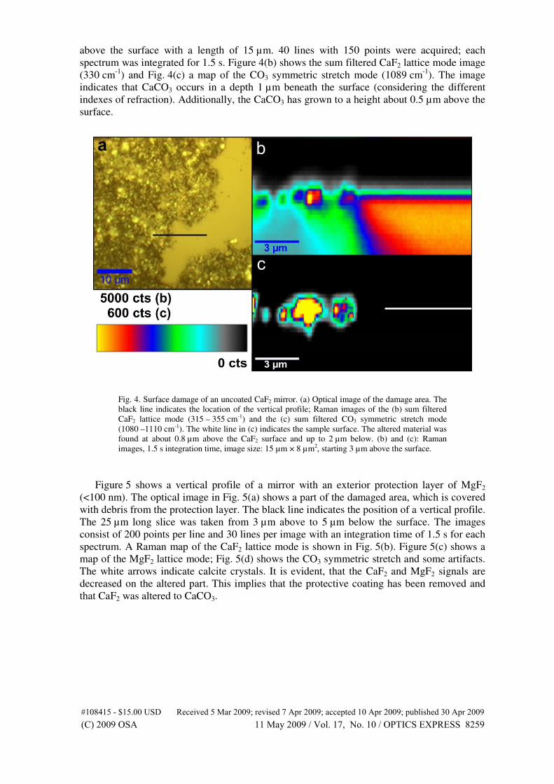
!""# $"%&'#( $")*%+ $" , !$(-. !"/"# $"%&/#( ( & !! 0.++102&!+" )%3!4( + %(-(! -" (!" *. ! 3! $"%( %5+ !3!( ! $"6789:7;<=<>7;?88<@AB CDEDFGDH<;<IJK<L88MN<KDGFODH<P<QRK<L88MN<JEEDRSDH<78<QRK<L88MN<RTUVFOWDH<X8<QRK<L88MYZ[\] _\ab cc\def\] _\g\hijk\clm\\nik\c\g\opqZa\rsotraa\\u]v_
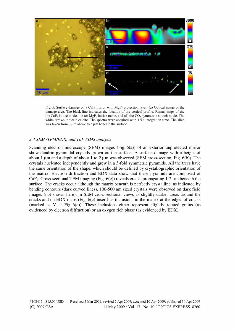
!" # # $ % & $'!' ()*)(+,-(./,-.,012(345(/678+9-+(343:;<=<( > ?@ A &' &' ! > B #? $B A ! # @> >CD B >?! &B' @ # ! &EEBEE F ! #> B ! >CD ? @ G? ! @ ! >CDHIJKLIMNONPIMQJJNRST UVWVXYVZNMN[\]NJJ_N]VYXaVZNbNcd]NJJ_N\WWVdeVZNIJNcd]NJJ_NdfghXaiVZNjJNcd]NJJ_klmnoppqnrst uunvwxnoppqnynz|nu~nnnupnynrlsnssnnop
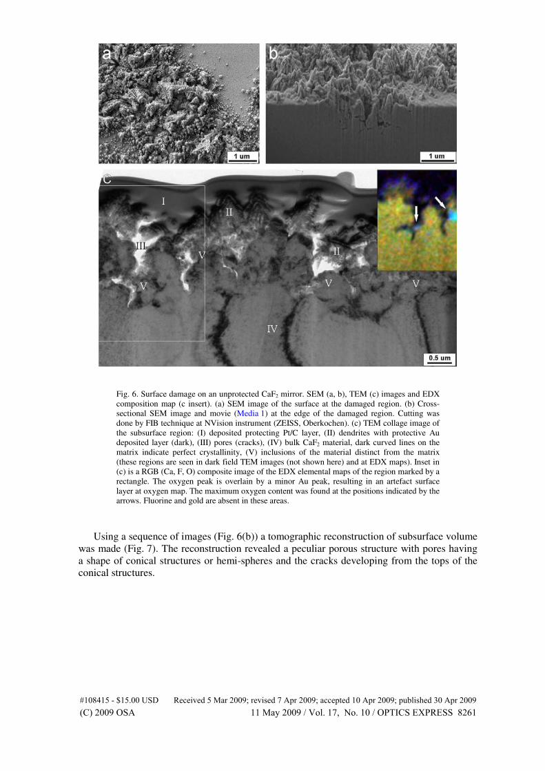
! " # $ %&'()*+&,-!!.& /0!%&& $"1 !% -&&&-&*!-! -" !2 %!!%*!! 2 -! $ &34',!!- %!2%-"!%1-!!%2%22%$ %$! ! 5("!$ 6"! !$"! - "!!789:;8<=>=?8<@99=ABC DEFEGHEI=<=JKL=M99NO=LEHGPEI=Q=RSL=M99NO=KFFESTEI=89=RSL=M99NO=SUVWGPXEI=Y9=RSL=M99NZ[\]__]abc dd]efg]__]h]ijkl]dmn]]ojl]d_]h]apqr[b]stpusbb]]vwd
!"# $%&'& (% (% ) *"+,- *.,+/- *0+//-1 !2)"3"01*04 *(4*4+2!**4" ! **4"56789:;<=;;:>?8( #@A ! (*0 ) **4"12 ( $2 !2 B0,C %( ( D 0 0 0 00 0 " 00 ) 1) 1 0 0EFG HI EI EFIHG HG EIEFIH HG EI EFEI HG HIJ J K J J KK J J K J J ).1! !)L.MN*1@A)/0A1!HG!(* (*)4+10( ' & OPQRSPTUVUWPTXQQUYZ[ \]]_]aUTUbcdUeQQfgUd]_h]aUiUjkdUeQQfgUc ]kl]aUPQUjkdUeQQfgUkmno_hp]aUqQUjkdUeQQfrstuvwwxuyz ||u~uvwwxuuu|uuu|wuuyszuzzuuvv
!"#$% &'( ) *'+,% -./0( &'( &&12 % +, & &&123 4 5 ' 670689 '%:;7:< &&12& 5 &&12 => = &'(: ? @ AB!CDEFCGH < I'7 6 53J7J'4 ) 'K+93'LMNO2P-Q2R4H <,8;%MS1 T ) S+ 8 % < J 5 6OQ2TH U5 3+ /4670689% 8>3MP:4';J' <IH<6<< I>'%:;7:VWXYZW[\]\W[_XX\ab cdedfgdh\[\ijk\lXXmn\kdgfodh\p\qrk\lXXmn\jeedrsdh\WX\qrk\lXXmn\rtuvfowdh\xX\qrk\lXXmyz|~~| ||~~||||||~||z|||

94 Optics Express
Optics Letters 95
7.5 Onset of the optical damage in CaF2 optics
caused by deep-UV lasers
Michael Bauer, Martin Bischoff, Thomas Hulsenbusch, Ansgar Matern,
and Robert W. Stark, Norbert Kaiser
Optics Letters Vol. 34, Iss. 24, pp. 3815 - 3817
Permanent weblink:
http://dx.doi.org/10.1364/OL.34.003815

96 Optics Letters
Onset of the optical damage in CaF2 opticscaused by deep-UV lasers
Michael Bauer,1,* Martin Bischoff,3 Thomas Hülsenbusch,2 Ansgar Matern,2
Robert W. Stark,1 and Norbert Kaiser3
1Center for NanoScience (CeNS) and Department of Earth and Environmental Sciences,Ludwig-Maximilians-Universität München, Theresienstrasse 41, 80333 Munich, Germany
2Coherent GmbH, Zielstattstraße 32, 81379 Munich, Germany3Fraunhofer-Institut für Angewandte Optik und Feinmechanik IOF, Albert-Einstein-Strasse 7, 07745 Jena, Germany
*Corresponding author: [email protected]
Received August 31, 2009; accepted October 30, 2009;posted November 13, 2009 (Doc. ID 116524); published December 7, 2009
The exterior sides of calcium fluoride CaF2 outcoupling mirrors are damaged by ArF laser light irradiationwith high pulse-energy densities 80 mJ/cm2. The damage is generated by a partial alteration of the CaF2substrate to calcite. The CaF2 decomposition is driven by photochemical processes due to the UV light andthe presence of water vapor and is supported by elevated temperatures within the laser beam transmittingarea. Small filaments act as starting points for the decomposition process, where kerogenous carbon andcalcite can occur. © 2009 Optical Society of America
OCIS codes: 140.3330, 230.4040, 140.2180, 260.7200.
Intense ultraviolet (UV) laser light used in variousareas such as lithography, metrology, medicine, andhigh-power industrial applications can degrade opti-cal components [1–4]. In particular, high-fluxdeep-UV (DUV) lasers generate damage structureson calcium fluoride CaF2 windows already afterrather short exposure times [3]. Within the surfacearea of the transmitted laser beam a white film formson the exterior surface [5]. The high-energy photonflux induces photochemical reactions at imperfec-tions or of contaminants from the environment withthe window material [6]. Controlled studies on the in-fluence of contaminants and the presence of watershow that uncoated CaF2 is attacked by water withinseveral hours [2,7]. Thus, a precise knowledge of theearly stages of material alteration is required to de-velop optics and protective coatings with increasedlifetime.
Recent investigations showed that a partial decom-position of the CaF2 bulk material into crystallinecalcium carbonate (CaCO3, calcite) is responsible forthe damage [6,8]. The decomposition is mainly drivenby photochemical processes in the presence of watervapor. The main parameters are high-UV photonenergy (6.42 eV, 193 nm), short pulse duration12 ns, high pulse power density, and elevatedtemperatures. The temperature of the mirror risesshortly before the material alteration becomes visu-ally evident. An increase from about 70°C to morethan 150°C was measured at 1 mm distance fromthe irradiated surface area. Chemical surface analy-sis revealed oxygen-rich phases within the damagearea including calcium oxide (CaO), which is verylikely a precursor for the alteration to CaCO3. BothCaO and CaCO3 adsorb in the UV region and thusmay expedite the damage process. In addition, a va-riety of organic materials could be observed such asnitrogen- and oxygen-bearing hydrocarbons and trig-lyceride. The first stages of the degradation process,however, are not yet understood.
In the following we show that the damage processis initiated by small dendritic filaments growing onthe exterior surface within the surface area of thetransmitted laser beam. To investigate this process,CaF2 outcoupling test mirrors (diameter 38.1 mm,thickness 5 mm, no protective coating) were loadedinto the mirror mount and sealed with an O-ring. Thedeposition of dust produced by electrode abrasionduring discharge was minimized with a stream of fil-tered laser gas on the resonator’s internal side. Toprevent the generation of oxygen radicals and ozonein front of the optics, the external optical path wasflushed with high-purity nitrogen. All componentswere made from stainless steel. Contaminations wereavoided by carefully handling the components in aclean environment. The samples were exposed to UVlight from an argon fluoride excimer laser [ArF,193 nm, 6.42 eV, 12 ns pulse duration (FWHM), Co-herent, Munich, Germany]. All measurements werecarried out in an energy-stabilized mode at 1 kHz incontinuous operation at an output pulse energy of28 mJ (80 mJ/cm2, 6 MW/cm2 pulse peak power).
The laser emission was stopped after approxi-mately 100 million laser pulses, and the outcouplingmirror was examined. A visual inspection revealeddamage structures smaller than those found after anexposure to more than 250 million laser pulses [8].Small individual filament structures as well as fila-ments that were connected to damage structures oc-curred after 100 million pulses. To clarify the damagemechanism we inspected these structures in more de-tail.
For compositional mapping the surface was imagedwith a confocal Raman microscope, alpha300 R(WITec, Ulm, Germany). The system used a standard100microscope objective (Air, NA=0.90, workingdistance 0.26 mm, Nikon, Düsseldorf, Germany) fordiffraction-limited focusing and collecting the scat-tered light from a frequency-doubled Nd:YAG(532 nm, 22 mW) laser. The inelastically scattered
December 15, 2009 / Vol. 34, No. 24 / OPTICS LETTERS 3815
0146-9592/09/243815-3/$15.00 © 2009 Optical Society of America
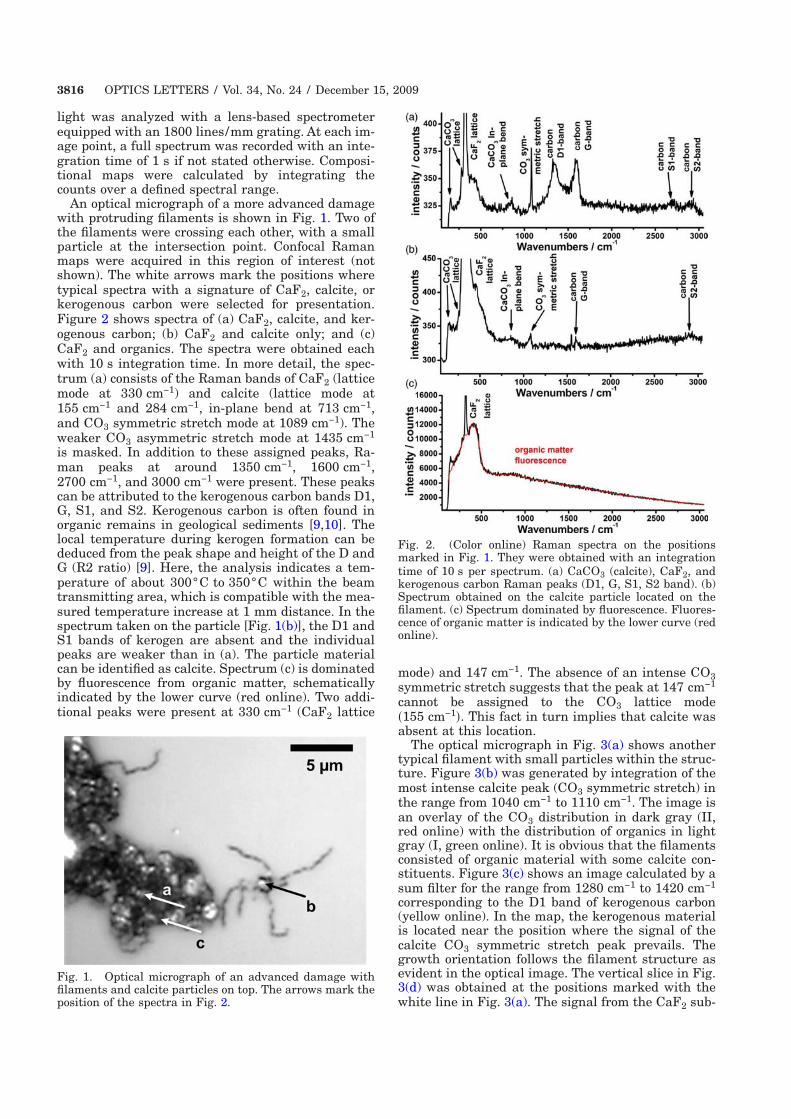
light was analyzed with a lens-based spectrometerequipped with an 1800 lines/mm grating. At each im-age point, a full spectrum was recorded with an inte-gration time of 1 s if not stated otherwise. Composi-tional maps were calculated by integrating thecounts over a defined spectral range.
An optical micrograph of a more advanced damagewith protruding filaments is shown in Fig. 1. Two ofthe filaments were crossing each other, with a smallparticle at the intersection point. Confocal Ramanmaps were acquired in this region of interest (notshown). The white arrows mark the positions wheretypical spectra with a signature of CaF2, calcite, orkerogenous carbon were selected for presentation.Figure 2 shows spectra of (a) CaF2, calcite, and ker-ogenous carbon; (b) CaF2 and calcite only; and (c)CaF2 and organics. The spectra were obtained eachwith 10 s integration time. In more detail, the spec-trum (a) consists of the Raman bands of CaF2 (latticemode at 330 cm−1) and calcite (lattice mode at155 cm−1 and 284 cm−1, in-plane bend at 713 cm−1,and CO3 symmetric stretch mode at 1089 cm−1). Theweaker CO3 asymmetric stretch mode at 1435 cm−1
is masked. In addition to these assigned peaks, Ra-man peaks at around 1350 cm−1, 1600 cm−1,2700 cm−1, and 3000 cm−1 were present. These peakscan be attributed to the kerogenous carbon bands D1,G, S1, and S2. Kerogenous carbon is often found inorganic remains in geological sediments [9,10]. Thelocal temperature during kerogen formation can bededuced from the peak shape and height of the D andG (R2 ratio) [9]. Here, the analysis indicates a tem-perature of about 300°C to 350°C within the beamtransmitting area, which is compatible with the mea-sured temperature increase at 1 mm distance. In thespectrum taken on the particle [Fig. 1(b)], the D1 andS1 bands of kerogen are absent and the individualpeaks are weaker than in (a). The particle materialcan be identified as calcite. Spectrum (c) is dominatedby fluorescence from organic matter, schematicallyindicated by the lower curve (red online). Two addi-tional peaks were present at 330 cm−1 (CaF2 lattice
mode) and 147 cm−1. The absence of an intense CO3symmetric stretch suggests that the peak at 147 cm−1
cannot be assigned to the CO3 lattice mode155 cm−1. This fact in turn implies that calcite wasabsent at this location.
The optical micrograph in Fig. 3(a) shows anothertypical filament with small particles within the struc-ture. Figure 3(b) was generated by integration of themost intense calcite peak (CO3 symmetric stretch) inthe range from 1040 cm−1 to 1110 cm−1. The image isan overlay of the CO3 distribution in dark gray (II,red online) with the distribution of organics in lightgray (I, green online). It is obvious that the filamentsconsisted of organic material with some calcite con-stituents. Figure 3(c) shows an image calculated by asum filter for the range from 1280 cm−1 to 1420 cm−1
corresponding to the D1 band of kerogenous carbon(yellow online). In the map, the kerogenous materialis located near the position where the signal of thecalcite CO3 symmetric stretch peak prevails. Thegrowth orientation follows the filament structure asevident in the optical image. The vertical slice in Fig.3(d) was obtained at the positions marked with thewhite line in Fig. 3(a). The signal from the CaF2 sub-
Fig. 1. Optical micrograph of an advanced damage withfilaments and calcite particles on top. The arrows mark theposition of the spectra in Fig. 2.
Fig. 2. (Color online) Raman spectra on the positionsmarked in Fig. 1. They were obtained with an integrationtime of 10 s per spectrum. (a) CaCO3 (calcite), CaF2, andkerogenous carbon Raman peaks (D1, G, S1, S2 band). (b)Spectrum obtained on the calcite particle located on thefilament. (c) Spectrum dominated by fluorescence. Fluores-cence of organic matter is indicated by the lower curve (redonline).
3816 OPTICS LETTERS / Vol. 34, No. 24 / December 15, 2009
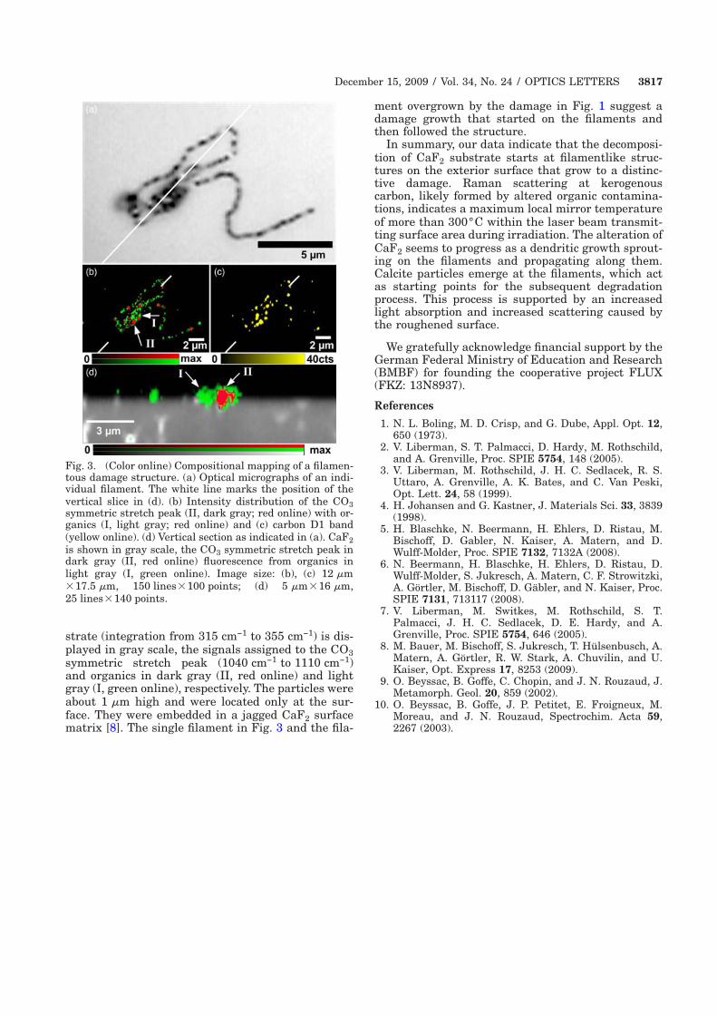
strate (integration from 315 cm−1 to 355 cm−1) is dis-played in gray scale, the signals assigned to the CO3symmetric stretch peak (1040 cm−1 to 1110 cm−1)and organics in dark gray (II, red online) and lightgray (I, green online), respectively. The particles wereabout 1 m high and were located only at the sur-face. They were embedded in a jagged CaF2 surfacematrix [8]. The single filament in Fig. 3 and the fila-
ment overgrown by the damage in Fig. 1 suggest adamage growth that started on the filaments andthen followed the structure.
In summary, our data indicate that the decomposi-tion of CaF2 substrate starts at filamentlike struc-tures on the exterior surface that grow to a distinc-tive damage. Raman scattering at kerogenouscarbon, likely formed by altered organic contamina-tions, indicates a maximum local mirror temperatureof more than 300°C within the laser beam transmit-ting surface area during irradiation. The alteration ofCaF2 seems to progress as a dendritic growth sprout-ing on the filaments and propagating along them.Calcite particles emerge at the filaments, which actas starting points for the subsequent degradationprocess. This process is supported by an increasedlight absorption and increased scattering caused bythe roughened surface.
We gratefully acknowledge financial support by theGerman Federal Ministry of Education and Research(BMBF) for founding the cooperative project FLUX(FKZ: 13N8937).
References
1. N. L. Boling, M. D. Crisp, and G. Dube, Appl. Opt. 12,650 (1973).
2. V. Liberman, S. T. Palmacci, D. Hardy, M. Rothschild,and A. Grenville, Proc. SPIE 5754, 148 (2005).
3. V. Liberman, M. Rothschild, J. H. C. Sedlacek, R. S.Uttaro, A. Grenville, A. K. Bates, and C. Van Peski,Opt. Lett. 24, 58 (1999).
4. H. Johansen and G. Kastner, J. Materials Sci. 33, 3839(1998).
5. H. Blaschke, N. Beermann, H. Ehlers, D. Ristau, M.Bischoff, D. Gabler, N. Kaiser, A. Matern, and D.Wulff-Molder, Proc. SPIE 7132, 7132A (2008).
6. N. Beermann, H. Blaschke, H. Ehlers, D. Ristau, D.Wulff-Molder, S. Jukresch, A. Matern, C. F. Strowitzki,A. Görtler, M. Bischoff, D. Gäbler, and N. Kaiser, Proc.SPIE 7131, 713117 (2008).
7. V. Liberman, M. Switkes, M. Rothschild, S. T.Palmacci, J. H. C. Sedlacek, D. E. Hardy, and A.Grenville, Proc. SPIE 5754, 646 (2005).
8. M. Bauer, M. Bischoff, S. Jukresch, T. Hülsenbusch, A.Matern, A. Görtler, R. W. Stark, A. Chuvilin, and U.Kaiser, Opt. Express 17, 8253 (2009).
9. O. Beyssac, B. Goffe, C. Chopin, and J. N. Rouzaud, J.Metamorph. Geol. 20, 859 (2002).
10. O. Beyssac, B. Goffe, J. P. Petitet, E. Froigneux, M.Moreau, and J. N. Rouzaud, Spectrochim. Acta 59,2267 (2003).
Fig. 3. (Color online) Compositional mapping of a filamen-tous damage structure. (a) Optical micrographs of an indi-vidual filament. The white line marks the position of thevertical slice in (d). (b) Intensity distribution of the CO3symmetric stretch peak (II, dark gray; red online) with or-ganics (I, light gray; red online) and (c) carbon D1 band(yellow online). (d) Vertical section as indicated in (a). CaF2is shown in gray scale, the CO3 symmetric stretch peak indark gray (II, red online) fluorescence from organics inlight gray (I, green online). Image size: (b), (c) 12 m17.5 m, 150 lines100 points; (d) 5 m16 m,25 lines140 points.
December 15, 2009 / Vol. 34, No. 24 / OPTICS LETTERS 3817

100 Optics Letters
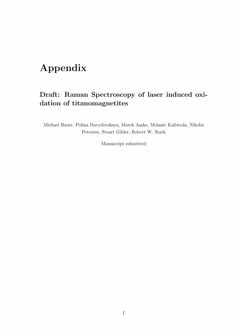
Appendix
Draft: Raman Spectroscopy of laser induced oxi-
dation of titanomagnetites
Michael Bauer, Polina Davydovskaya, Marek Janko, Melanie Kaliwoda, Nikolai
Petersen, Stuart Gilder, Robert W. Stark
Manuscript submitted
I

II Appendix
1
Raman spectroscopy of laser induced oxidation of
titanomagnetites
Michael Bauer1,2
, Polina Davydovskaya1,2
, Marek Janko1,2
, Melanie Kaliwoda3, Nikolai
Petersen1, Stuart Gilder
1, Robert W. Stark
2,4,5,*
1 Department of Earth and Environmental Sciences, Ludwig-Maximilians-Universität München, Theresienstr. 41, 80333
Munich, Germany 2 Center for NanoScience (CeNS), Schellingstr. 4, 80799 Munich, Germany
3 Mineralogical State Collection, LMU, Theresienstrasse 41, 80333 Munich, Germany 4 FB Material- und Geowissenschaften, TU Darmstadt, Petersenstr. 32, 64287 Darmstadt, Germany
5 Center for Smart Interfaces, TU Darmstadt, Petersenstr. 32, 64287 Darmstadt, Germany
*corresponding author: Phone: +49 6151 16 2109, Fax: +49 6151 16 72090, e-mail: [email protected]
Abstract: Titanomagnetites are important carriers of magnetic remanence in nature and can
track redox conditions in magma. The titanium concentration in magnetite bears heavily on its
magnetic properties, such as saturation moment and Curie temperature. On land and in the deep
ocean, however, these minerals are prone to alteration which can mask the primary magnetic
signals they once recorded. Thus, it is essential to characterize the cation composition and
oxidation state of titanomagnetites that record the paleomagnetic field. Raman spectroscopy
provides a unique tool for both purposes. Nonetheless, the heat generated by the Raman laser
can itself induce oxidation. We show that the laser power threshold to produce oxidation
decreases with increasing titanium content. With confocal Raman spectroscopy and magnetic
force microscopy on natural and synthetic titanomagnetites, non-destructive Raman imaging
protocol was established. We applied this protocol to map out the composition and
magnetization state within a single ex-solved titanomagnetite grain in a deep sea basalt.
Keywords: titanomagnetite, alterations, local heating, MFM, confocal Raman
1. Introduction The composition of magnetic minerals provides information on the conditions of rock genesis
and alteration.[1]
Minerals from the titanomagnetite solid solution series (Fe3-xTixO4, 0 < x < 1)
are of particular relevance because they carry the remanent magnetization of oceanic basalts.[2, 3]
The composition of titanomagnetite is close to x = 0.6 with a Curie temperature of 140 °C when
formed at a spreading ridge.[1]
Their equilibrium oxygen fugacity is on the order of 10-7
atm,
implying a strong tendency to oxidize under sea-floor conditions.[4]
To characterize the
composition and oxidation state of titanomagnetite Raman imaging techniques are valuable
tools.[5]
Raman spectroscopic characterization and compositional analysis of rock-forming
minerals will also be an important tool in future planetary missions.[6, 7]
Iron oxides, however,
are poor Raman scatterers that strongly absorb in the range of the wavelengths of typical
excitation lasers and high laser intensities are required to obtain an adequate signal.[1, 8]
Thus,
the heat generated by the strongly focussed Raman laser may lead to alteration. To obtain
reliable Raman data on titanomagnetite, the measurement conditions need to be optimized to
reduce the measurement time without altering of the specimen.
Stoichiometric titanomagnetites (Fe3-xTixO4) can be synthesized in a wide range of
compositions.[9]
Magnetite, i.e. x = 0, also referred to as TM00, is a special case of ferrite with
the general formula Fe2+
Fe23+
O4 corresponding to FeO⋅Fe2O3 (simplified Fe3O4) with an inverse
spinel structure.[10]
TM60 (x = 0.6) represents an idealized natural titanomagnetite with the
composition Fe2.4Ti0.6O4. The long range order in synthetic TM60 single crystals is a function of
nonstoichiometry with higher cation vacancy concentrations producing a more random cation
distribution.[11]
The magnetic stability of synthetic titanomagnetite can be increased by oxidation
and subsequent annealing in vacuum.[12]
Natural titanomagnetite often intergrows with ilmenite
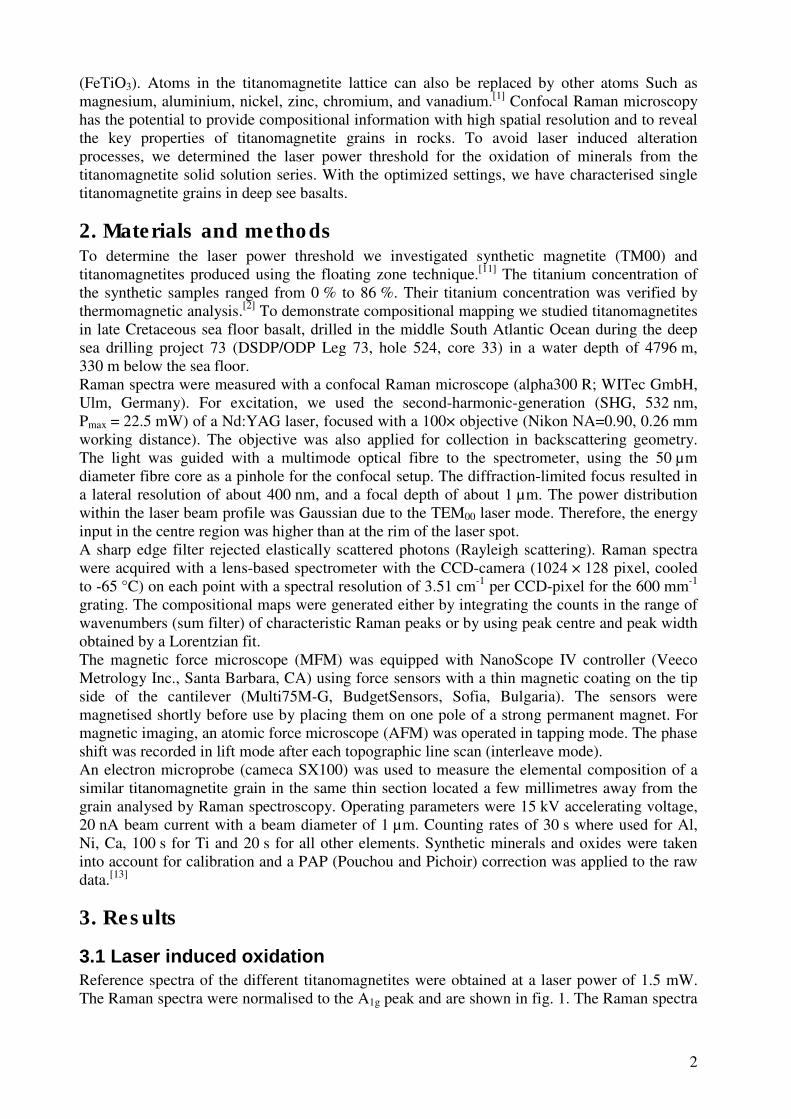
2
(FeTiO3). Atoms in the titanomagnetite lattice can also be replaced by other atoms Such as
magnesium, aluminium, nickel, zinc, chromium, and vanadium.[1]
Confocal Raman microscopy
has the potential to provide compositional information with high spatial resolution and to reveal
the key properties of titanomagnetite grains in rocks. To avoid laser induced alteration
processes, we determined the laser power threshold for the oxidation of minerals from the
titanomagnetite solid solution series. With the optimized settings, we have characterised single
titanomagnetite grains in deep see basalts.
2. Materials and methods To determine the laser power threshold we investigated synthetic magnetite (TM00) and
titanomagnetites produced using the floating zone technique.[11]
The titanium concentration of
the synthetic samples ranged from 0 % to 86 %. Their titanium concentration was verified by
thermomagnetic analysis.[2]
To demonstrate compositional mapping we studied titanomagnetites
in late Cretaceous sea floor basalt, drilled in the middle South Atlantic Ocean during the deep
sea drilling project 73 (DSDP/ODP Leg 73, hole 524, core 33) in a water depth of 4796 m,
330 m below the sea floor.
Raman spectra were measured with a confocal Raman microscope (alpha300 R; WITec GmbH,
Ulm, Germany). For excitation, we used the second-harmonic-generation (SHG, 532 nm,
Pmax = 22.5 mW) of a Nd:YAG laser, focused with a 100× objective (Nikon NA=0.90, 0.26 mm
working distance). The objective was also applied for collection in backscattering geometry.
The light was guided with a multimode optical fibre to the spectrometer, using the 50 µm
diameter fibre core as a pinhole for the confocal setup. The diffraction-limited focus resulted in
a lateral resolution of about 400 nm, and a focal depth of about 1 µm. The power distribution
within the laser beam profile was Gaussian due to the TEM00 laser mode. Therefore, the energy
input in the centre region was higher than at the rim of the laser spot.
A sharp edge filter rejected elastically scattered photons (Rayleigh scattering). Raman spectra
were acquired with a lens-based spectrometer with the CCD-camera (1024 × 128 pixel, cooled
to -65 °C) on each point with a spectral resolution of 3.51 cm-1
per CCD-pixel for the 600 mm-1
grating. The compositional maps were generated either by integrating the counts in the range of
wavenumbers (sum filter) of characteristic Raman peaks or by using peak centre and peak width
obtained by a Lorentzian fit.
The magnetic force microscope (MFM) was equipped with NanoScope IV controller (Veeco
Metrology Inc., Santa Barbara, CA) using force sensors with a thin magnetic coating on the tip
side of the cantilever (Multi75M-G, BudgetSensors, Sofia, Bulgaria). The sensors were
magnetised shortly before use by placing them on one pole of a strong permanent magnet. For
magnetic imaging, an atomic force microscope (AFM) was operated in tapping mode. The phase
shift was recorded in lift mode after each topographic line scan (interleave mode).
An electron microprobe (cameca SX100) was used to measure the elemental composition of a
similar titanomagnetite grain in the same thin section located a few millimetres away from the
grain analysed by Raman spectroscopy. Operating parameters were 15 kV accelerating voltage,
20 nA beam current with a beam diameter of 1 µm. Counting rates of 30 s where used for Al,
Ni, Ca, 100 s for Ti and 20 s for all other elements. Synthetic minerals and oxides were taken
into account for calibration and a PAP (Pouchou and Pichoir) correction was applied to the raw
data.[13]
3. Results
3.1 Laser induced oxidation
Reference spectra of the different titanomagnetites were obtained at a laser power of 1.5 mW.
The Raman spectra were normalised to the A1g peak and are shown in fig. 1. The Raman spectra
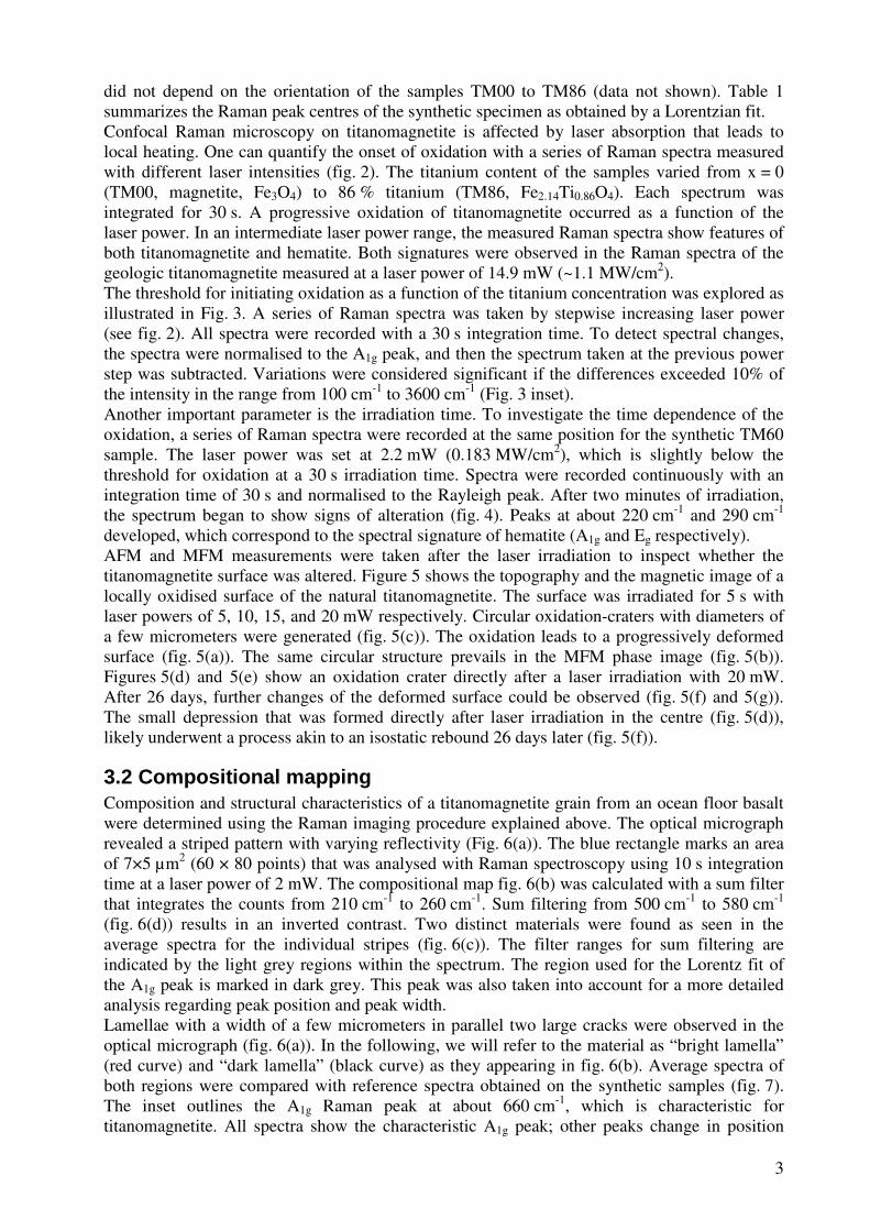
3
did not depend on the orientation of the samples TM00 to TM86 (data not shown). Table 1
summarizes the Raman peak centres of the synthetic specimen as obtained by a Lorentzian fit.
Confocal Raman microscopy on titanomagnetite is affected by laser absorption that leads to
local heating. One can quantify the onset of oxidation with a series of Raman spectra measured
with different laser intensities (fig. 2). The titanium content of the samples varied from x = 0
(TM00, magnetite, Fe3O4) to 86 % titanium (TM86, Fe2.14Ti0.86O4). Each spectrum was
integrated for 30 s. A progressive oxidation of titanomagnetite occurred as a function of the
laser power. In an intermediate laser power range, the measured Raman spectra show features of
both titanomagnetite and hematite. Both signatures were observed in the Raman spectra of the
geologic titanomagnetite measured at a laser power of 14.9 mW (~1.1 MW/cm2).
The threshold for initiating oxidation as a function of the titanium concentration was explored as
illustrated in Fig. 3. A series of Raman spectra was taken by stepwise increasing laser power
(see fig. 2). All spectra were recorded with a 30 s integration time. To detect spectral changes,
the spectra were normalised to the A1g peak, and then the spectrum taken at the previous power
step was subtracted. Variations were considered significant if the differences exceeded 10% of
the intensity in the range from 100 cm-1
to 3600 cm-1
(Fig. 3 inset).
Another important parameter is the irradiation time. To investigate the time dependence of the
oxidation, a series of Raman spectra were recorded at the same position for the synthetic TM60
sample. The laser power was set at 2.2 mW (0.183 MW/cm2), which is slightly below the
threshold for oxidation at a 30 s irradiation time. Spectra were recorded continuously with an
integration time of 30 s and normalised to the Rayleigh peak. After two minutes of irradiation,
the spectrum began to show signs of alteration (fig. 4). Peaks at about 220 cm-1
and 290 cm-1
developed, which correspond to the spectral signature of hematite (A1g and Eg respectively).
AFM and MFM measurements were taken after the laser irradiation to inspect whether the
titanomagnetite surface was altered. Figure 5 shows the topography and the magnetic image of a
locally oxidised surface of the natural titanomagnetite. The surface was irradiated for 5 s with
laser powers of 5, 10, 15, and 20 mW respectively. Circular oxidation-craters with diameters of
a few micrometers were generated (fig. 5(c)). The oxidation leads to a progressively deformed
surface (fig. 5(a)). The same circular structure prevails in the MFM phase image (fig. 5(b)).
Figures 5(d) and 5(e) show an oxidation crater directly after a laser irradiation with 20 mW.
After 26 days, further changes of the deformed surface could be observed (fig. 5(f) and 5(g)).
The small depression that was formed directly after laser irradiation in the centre (fig. 5(d)),
likely underwent a process akin to an isostatic rebound 26 days later (fig. 5(f)).
3.2 Compositional mapping
Composition and structural characteristics of a titanomagnetite grain from an ocean floor basalt
were determined using the Raman imaging procedure explained above. The optical micrograph
revealed a striped pattern with varying reflectivity (Fig. 6(a)). The blue rectangle marks an area
of 7×5 µm2 (60 × 80 points) that was analysed with Raman spectroscopy using 10 s integration
time at a laser power of 2 mW. The compositional map fig. 6(b) was calculated with a sum filter
that integrates the counts from 210 cm-1
to 260 cm-1
. Sum filtering from 500 cm-1
to 580 cm-1
(fig. 6(d)) results in an inverted contrast. Two distinct materials were found as seen in the
average spectra for the individual stripes (fig. 6(c)). The filter ranges for sum filtering are
indicated by the light grey regions within the spectrum. The region used for the Lorentz fit of
the A1g peak is marked in dark grey. This peak was also taken into account for a more detailed
analysis regarding peak position and peak width.
Lamellae with a width of a few micrometers in parallel two large cracks were observed in the
optical micrograph (fig. 6(a)). In the following, we will refer to the material as “bright lamella”
(red curve) and “dark lamella” (black curve) as they appearing in fig. 6(b). Average spectra of
both regions were compared with reference spectra obtained on the synthetic samples (fig. 7).
The inset outlines the A1g Raman peak at about 660 cm-1
, which is characteristic for
titanomagnetite. All spectra show the characteristic A1g peak; other peaks change in position
4
(T2g(1), from ~190 cm-1
to ~150 cm-1
), appear (T2g(2), 480 cm-1
) or vanish (Eg, 310 cm-1
; T2g(3),
540 cm-1
and the peak at 850 cm-1
) with increasing titanium content.
Figure 8 correlates the chemical information of the Raman spectra with information determined
by AFM and MFM measurements on the geologic sample. The topography image in fig. 8(a)
also reveals a striped pattern, which implies differences in material hardness. The magnetic
image in fig. 8(b), show a clear stripe pattern alternating between magnetic and non-magnetic
phases. The Raman map in fig. 8(c) was obtained from the peak centre position of a Lorentz fit
on the A1g peak and also shows these stripes. The Lorentz fit results in better contrast with
decreased noise level as compared to the images calculated with the simple sum filter (fig. 6).
All images clearly show the identical lamellar pattern. The structures in the MFM image
correlate to the same structures as visible in the titanomagnetite distribution determined with
Raman spectroscopy. An elemental microprobe analysis of a similar natural titanomagnetite
revealed a slight exchange of magnesium against iron and a titanium and aluminium content that
fluctuated (data not shown).
4 Discussion
4.1. Laser power
The alteration threshold decreases with increasing titanium concentration. Depending on the
laser power, a partial oxidation could be observed within a certain range. Local temperatures
towards the centre of the laser spot induced alteration whereas oxidation did not occur near the
rim. In the spectrometer, however, scattered light from the centre and the surrounding region is
averaged. When analysing titanomagnetites of unknown composition, the laser power should be
limited to 1.5 mW (0.08 MW/cm2) with integration times of several minutes. At laser powers
<1.5 mW a safe mode of operation could be verified for the geologic and synthetic samples.
Only spectra taken at laser powers below this threshold should be used for an uncompromised
compositional analysis.
The results clearly show that laser-induced oxidation should be taken into account for a
spectroscopic characterization of (titano-)magnetites. In addition, one also might adjust the
oxygen fugacity during the measurement. Magnetite and titanomagnetite oxidise above ~240 °C
in a normal atmosphere.[8, 14, 15]
Raman measurements in an oxygen-free atmosphere might help
reduce the tendency to oxidise. It should be mentioned, however, that noble gases can diffuse
into synthetic magnetite above 500 °C during growth.[16]
At about 600 °C, a phase transition
from magnetite to other iron oxides can occur.[16-18]
Such high temperatures may be achieved at
high laser powers or strong focusing. For practical measurements under ambient conditions one
has to balance measurement time and laser power to avoid alteration.
4.2. Deep sea basalt
With these optimized settings the composition of a natural titanomagnetite was mapped
spectroscopically and two distinct phases was observed. A comparison with the reference
spectra obtained on the synthetic specimen revealed subtle differences, which makes the
identification of the mineral phases difficult. The peaks in the Raman spectra of the dark lamella
(black curve) match best to the TM20 reference spectrum (fig. 7). The peak centre (665 cm-1
) of
the A1g, also better agrees with that of TM20 (664 cm-1
). The peak width (74 cm-1
), however,
better matches to the width of the TM40 (76 cm-1
). The MFM measurements show that the dark
lamella is a magnetic phase. Thus, it is reasonable to assume that the dark lamella correspond to
a titanomagnetite with a titanium content around 20 % to 40 %.
The identification of the bright phase in fig. 6(b) is ambiguous. The relative intensities of the
T2g(2) and T2g(3) peaks match to the TM40 spectrum . The peak width (66 cm-1
) is between the
values for TM20 (54 cm-1
) and TM40 value. However, the peak at 235 cm-1
is missing in the
reference spectra of the synthetic minerals. Also the A1g peak position (673 cm-1
) does not fit
5
well to the respective peak position of the synthetic titanomagnetites. These results indicate that
the phase is most likely not a pure titanomagnetite phase but another iron oxide mineral. Various
Raman spectra are available in the literature for chemically related iron oxides. For example,
Faria et al. reported similar Raman spectra for a laser heated wüstite, where decomposition leads
to α-Fe and Fe3O4, and assumed that Fe3O4 has been transformed into hematite (α-Fe2O3).[14]
Raman spectra of maghemite (γ-Fe2O3), which can be seen as iron-deficient form of magnetite,
also coincide with that of the bright lamella.[19-21]
Ilmenite is another candidate because the
peaks at 235 cm-1
bright lamella and 229 cm-1
ilmenite match. However, there are discrepancies
for the A1g peak position (680 cm-1
for ilmenite) and in particular the peak at ~480 cm-1
, which
is not present in ilmenite. The bright lamella is not ferromagnetic because in MFM the bright
lamella does not show a signal (fig. 8(b)). Titanomagnetites with x = ~0.75 are paramagnetic at
room temperature, therefore such a titanomagnetite phase cannot be excluded with the MFM
measurements. However maghemite and ilmenite were disproved with MFM, given that both
phases are magnetic.
Microprobe data provides additional insights into the composition of the mineral phases. Also
the elemental composition showed an alternating exchange of ions. The variations may be
caused by growth-zoning in natural magnetite. It is reasonable to assume that the variation
observed by the microprobe measurement also affects the Raman spectra. The exchange of iron
and magnesium ions could explain the deviation of the spectrum of the bright lamella from a
pure mineral phase. The composition of that phase, however, remains an open question to
further study.
5. Conclusion Titanomagnetite Raman spectra vary in peak position, intensity and width as a function of
titanium concentration and degree of oxidation. Hence, Raman spectroscopy can identify the
composition and oxidation state of minerals of the magnetite-ülvospinel solid solution series.
Depending on the titanium content, the mineral starts to oxidise above a certain laser power
threshold. Adjusting the laser power just below the threshold for immediate oxidation is
insufficient because time-dependent oxidation processes can still occur. The laser heating causes
an altered spot on the surface whose diameter and height depends on the laser power and
irradiation time. Oxidation continues weeks after laser application. Laser power should be
maintained well under the threshold to avoid oxidation.
Based on these findings, we investigated a natural basalt collected from the deep ocean floor.
Compositional Raman mapping revealed a lamellar structure. One mineral phase can be
attributed to a titanomagnetite with a titanium content of about 20 % - 40 %. The other phase
could not be unambiguously identified.
Acknowledgements We thank Gloria Almonacid Caballer for fruitful discussions and the Deutsche
Forschungsgemeinschaft (DFG) for funding this project under grant STA 1026/2-1
6
References [1] A. Wang, K. E. Kuebler, B. L. Jolliff, L. A. Haskin, American Mineralogist 2004, 89,
665.
[2] S. A. Gilder, M. Le Goff, Geophys. Res. Lett. 2008, 35.
[3] M. Marshall, A. Cox, Nature 1971, 230, 28.
[4] J. Verhoogen, The Journal of Geology 1962, 70, 168.
[5] L. Tatsumi-Petrochilos, S. A. Gilder, P. Zinin, J. E. Hammer, M. D. Fuller, AGU Fall
Meeting Abstracts 2008, A791+.
[6] A. Ellery, D. Wynn-Williams, Astrobiology 2003, 3, 565.
[7] J. Popp, M. Schmitt, Journal of Raman Spectroscopy 2004, 35, 429.
[8] O. N. Shebanova, P. Lazor, Journal of Raman Spectroscopy 2003, 34, 845.
[9] H. C. Soffel, E. Appel, Physics of The Earth and Planetary Interiors 1982, 30, 348.
[10] L. V. Gasparov, D. B. Tanner, D. B. Romero, H. Berger, G. Margaritondo, L. Forro,
Physical Review B 2000, 62, 7939.
[11] B. J. Wanamaker, B. M. Moskowitz, Geophys. Res. Lett. 1994, 21.
[12] M. Lewis, Geophysical Journal of the Royal Astronomical Society 1968, 16, 295.
[13] J. L. Pouchou, F. Pichoir, La Recherche Aérospatiale 1984, 3, 13.
[14] D. L. A. d. Faria, S. V. Silva, M. T. d. Oliveira, Journal of Raman Spectroscopy 1997,
28, 873.
[15] B.-K. Kim, J. A. Szpunar, Scripta Materialia 2001, 44, 2605.
[16] T. Matsumoto, K. Maruo, A. Tsuchiyama, J.-I. Matsuda, Earth and Planetary Science
Letters 1996, 141, 315.
[17] D. P. Burke, R. L. Higginson, Scripta Materialia 2000, 42, 277.
[18] J. Tominaga, K. Wakimoto, T. Mori, M. Murakami, T. Yoshimura, Transactions of the
Iron and Steel Institute of Japan 1982, 22, 646.
[19] I. Chamritski, G. Burns, The Journal of Physical Chemistry B 2005, 109, 4965.
[20] J. C. Rubim, M. H. Sousa, J. C. O. Silva, F. A. Tourinho, Brazilian Journal of Physics
2001, 31, 402.
[21] M. H. Sousa, F. A. Tourinho, J. C. Rubim, Journal of Raman Spectroscopy 2000, 31,
185.
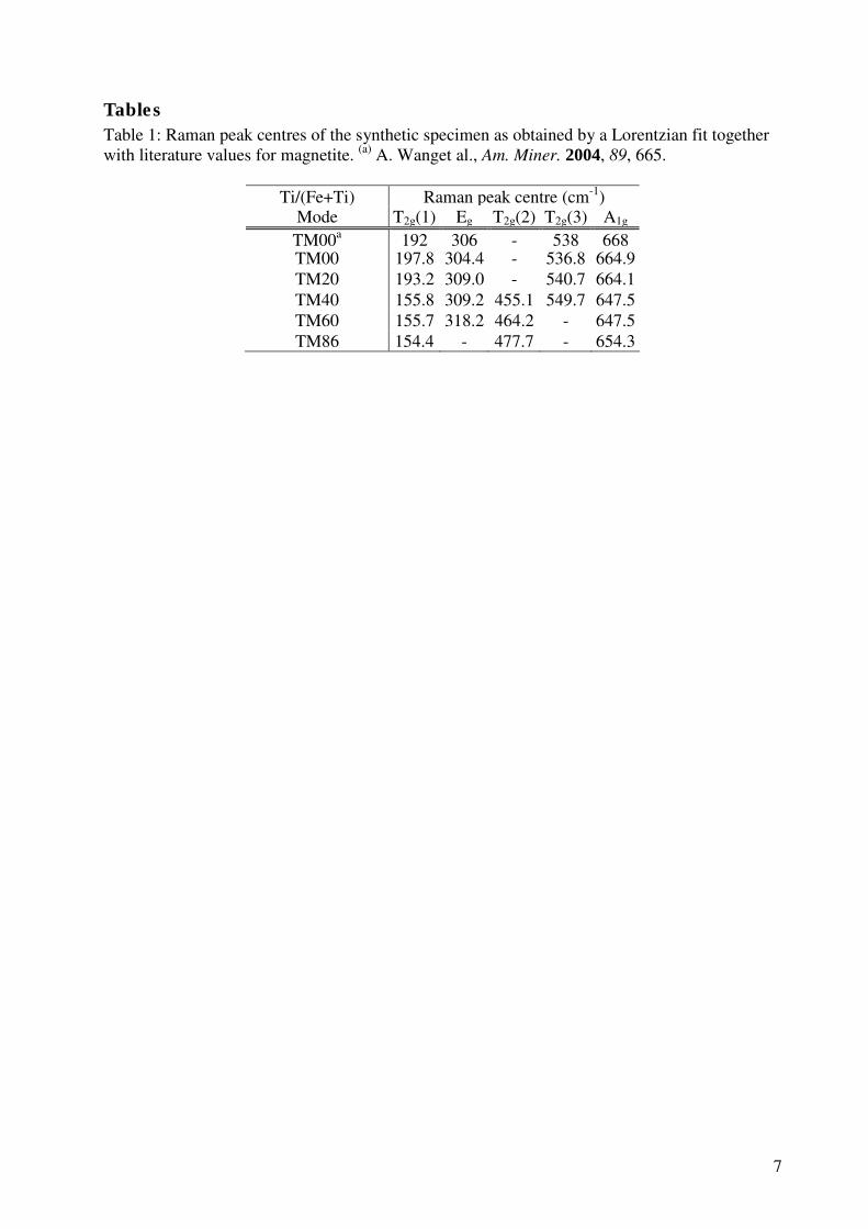
7
Tables
Table 1: Raman peak centres of the synthetic specimen as obtained by a Lorentzian fit together
with literature values for magnetite. (a)
A. Wanget al., Am. Miner. 2004, 89, 665.
Ti/(Fe+Ti) Raman peak centre (cm-1
) Mode T2g(1) Eg T2g(2) T2g(3) A1g
TM00a 192 306 - 538 668
TM00 197.8 304.4 - 536.8 664.9
TM20 193.2 309.0 - 540.7 664.1
TM40 155.8 309.2 455.1 549.7 647.5
TM60 155.7 318.2 464.2 - 647.5
TM86 154.4 - 477.7 - 654.3
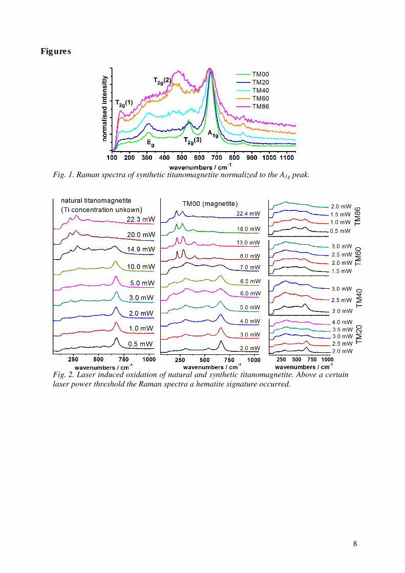
8
Figures
Fig. 1. Raman spectra of synthetic titanomagnetite normalized to the A1g peak.
Fig. 2. Laser induced oxidation of natural and synthetic titanomagnetite. Above a certain
laser power threshold the Raman spectra a hematite signature occurred.
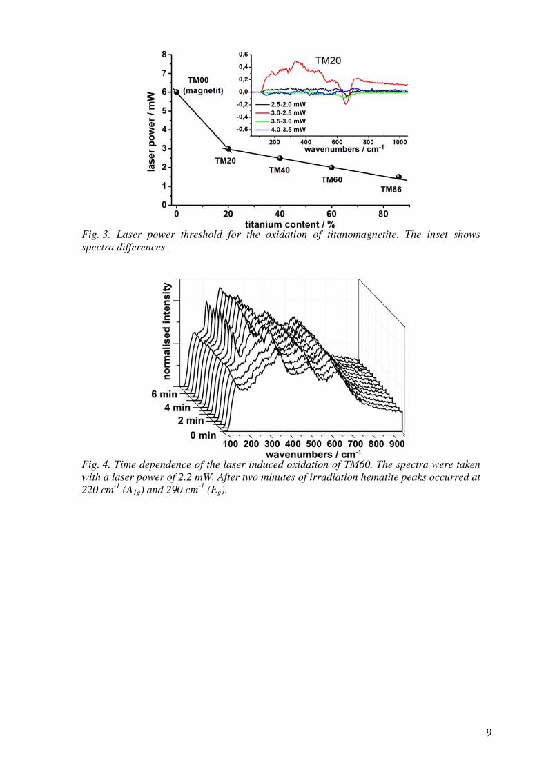
9
Fig. 3. Laser power threshold for the oxidation of titanomagnetite. The inset shows
spectra differences.
Fig. 4. Time dependence of the laser induced oxidation of TM60. The spectra were taken
with a laser power of 2.2 mW. After two minutes of irradiation hematite peaks occurred at
220 cm-1
(A1g) and 290 cm-1
(Eg).
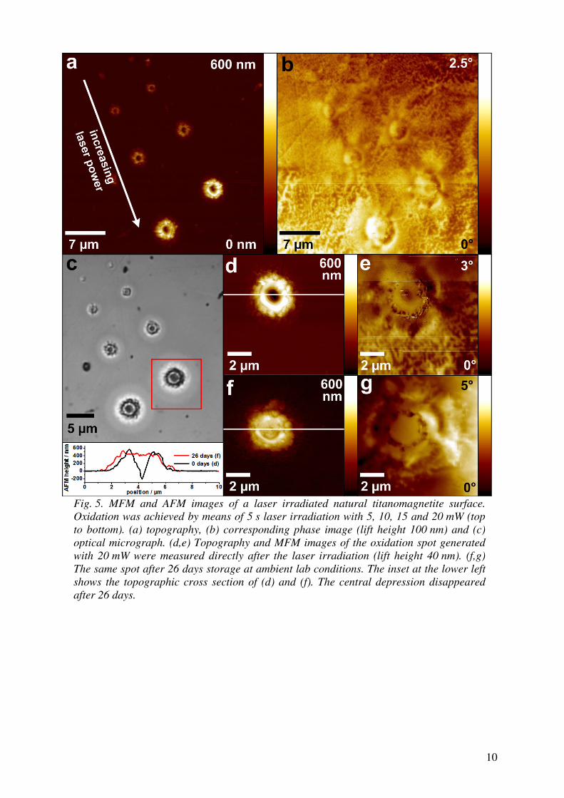
10
Fig. 5. MFM and AFM images of a laser irradiated natural titanomagnetite surface.
Oxidation was achieved by means of 5 s laser irradiation with 5, 10, 15 and 20 mW (top
to bottom). (a) topography, (b) corresponding phase image (lift height 100 nm) and (c)
optical micrograph. (d,e) Topography and MFM images of the oxidation spot generated
with 20 mW were measured directly after the laser irradiation (lift height 40 nm). (f,g)
The same spot after 26 days storage at ambient lab conditions. The inset at the lower left
shows the topographic cross section of (d) and (f). The central depression disappeared
after 26 days.
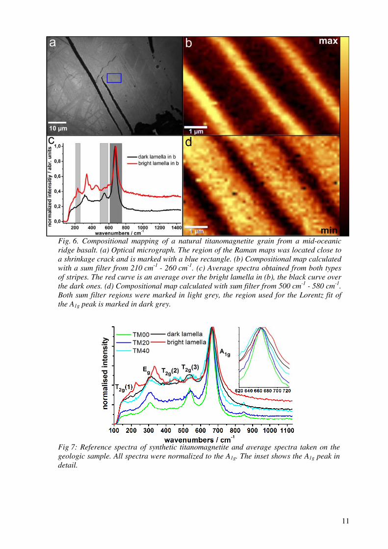
11
Fig. 6. Compositional mapping of a natural titanomagnetite grain from a mid-oceanic
ridge basalt. (a) Optical micrograph. The region of the Raman maps was located close to
a shrinkage crack and is marked with a blue rectangle. (b) Compositional map calculated
with a sum filter from 210 cm-1
- 260 cm-1
. (c) Average spectra obtained from both types
of stripes. The red curve is an average over the bright lamella in (b), the black curve over
the dark ones. (d) Compositional map calculated with sum filter from 500 cm-1
- 580 cm-1
.
Both sum filter regions were marked in light grey, the region used for the Lorentz fit of
the A1g peak is marked in dark grey.
Fig 7: Reference spectra of synthetic titanomagnetite and average spectra taken on the
geologic sample. All spectra were normalized to the A1g. The inset shows the A1g peak in
detail.
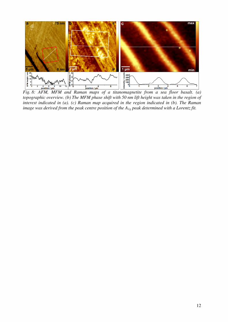
12
Fig. 8: AFM, MFM and Raman maps of a titanomagnetite from a sea floor basalt. (a)
topographic overview. (b) The MFM phase shift with 50 nm lift height was taken in the region of
interest indicated in (a). (c) Raman map acquired in the region indicated in (b). The Raman
image was derived from the peak centre position of the A1g peak determined with a Lorentz fit.
Acknowledgements
There are many people I would like to thank for their support that made this disser-
tation possible. First, I thank PD Dr. Robert Stark, who gave me the opportunity
to do research in his group and laboratories. With his guidance and encouragement
on individual topics and allowing me the freedom to work on my own subjects of
interest, I was able to create this thesis.
I am also grateful to Prof. Wolfgang Heckl, who let me start in his group, and to
Prof. Stefan Sotier, who made the contact.
Many thanks also go to Dr. Alexander Gigler for his assistance during the measure-
ments and the interpretation of the results. I am also grateful for the support of
the other members in the group (Marek Janko, Dr. Marc Hennemeyer, and Polina
Davydovskaya) and the entire parallel STM group of Prof. Markus Lackinger.
I enjoyed working together and discussing everything and, of course, having activities
outside of my scientific work.
In addition, I thank my colleagues in the Laser Discharge Unit of the former Tui-
Laser AG, in particular, Dr. Sebastian Sporlein, Dr. Claus Strowitzki, Alexandar
Djordevic, Dr. Andreas Gortler and Ansgar Mattern for giving me the chance to
work on the problems of deteriorating excimer optics. I thank them not only for
the experience with excimer laser systems and related technologies but also for their
excellent teamwork. It has been a great pleasure working with them for all these
years.
Last but not least, I thank my parents and my brother, who have supported me
throughout the preparation of this dissertation.
XV
XVI Curriculum Vitae
Curriculum Vitae
Personal
Name Michael Ludwig Bauer
Birth 1978
in Wurzburg
Education
since 2005 PhD candidate at the LMU Munchen
2002 - 2005 Master Study: Micro- and Nanotechnology
University of Applied Sciences Munich
qualification: Master of Engineering (M.Eng.)
1997 - 2002 Undergraduate Study: ’Physikalische Technik’
University of Applied Sciences Munich
qualification: Graduate engineer (Dipl.-Ing. (FH))
1994 - 1996 Technical college, Wurzburg, vocational baccalaureate diploma
1990 - 1994 Secondary school, Wurzburg, secondary school level
1984 - 1990 Primary school, Gerbrunn (Wurzburg)
Civil Service
1996 to 1997 Civil Service at”Sozialzentrum der Arbeiterwohlfahrt“, Wurzburg
Practical experience
since 2006 Homepage administration for the division”
Kurzzeitphysik“
of the Deutsche Physikalische Gesellschaft (DPG)
2006 - 2009 R & D Department at the Coherent GmbH
(acquisition of the TuiLaser AG)
2002 - 2006 R & D Department at the TuiLaser AG
2000 5 months internship at the Kayser-Threde GmbH, Munich
1999 Working student at the”Lehrstuhl fur Experimental Physik I“
Julius-Maximilian Universitat, Wurzburg
1998 - 1999 5 months internship at the”Lehrstuhl fur Experimental Physik I“
Julius-Maximilian Universitat, Wurzburg
Publication list XVII
Reviewed Publications
[1] H.P. Huber, M. Bauer, A.J. Gortler, C.F. Strowitzki, A. Hohla. Devel-opment of high-repetition-rate molecular fluorine lasers for metrology andinspection. Metrology, Inspection, and Process Control for Microlithogra-phy XVIII; Proceedings of SPIE Vol. 5375, 792 (Bellingham, WA, 2004);doi:10.1117/12.534062
[2] M. Bauer, A.M. Gigler, C. Richter, R.W. Stark. Visualizing stress in sil-icon microcantilevers using scanning confocal Raman spectroscopy. Micro-electronic Engineering, Volume 85, Issues 5-6, Pages 1443 - 1446, Proceed-ings of the Micro- and Nano-Engineering 2007 Conference - MNE 2007.doi:10.1016/j.mee.2008.01.089
[3] M. Bauer, A.M. Gigler, A.J. Huber, R. Hillenbrand and R.W. Stark. Temper-ature depending Raman line-shift of silicon carbide. Journal of Raman Spec-troscopy, 2009, Volume 40 Issue 12, Pages 1867 - 1874. doi:10.1002/jrs.2334
[4] M. Bauer, M. Bischoff, S. Jukresch, T. Hulsenbusch, A. Matern, A. Gortler,R.W. Stark and U. Kaiser. Exterior surface damage of calcium fluoride outcoupling mirrors for DUV lasers. Optics Express, Vol. 17, Issue 10, pp.8253 - 8263. doi:10.1364/OE.17.008253
[5] M. Bauer, M. Bischoff, T. Hulsenbusch, A. Matern and R.W. Stark, N. Kaiser.Onset of the optical damage in CaF2 optics caused by deep-UV lasers. OpticsLetters Vol. 34, Iss. 24, pp. 3815 - 3817. doi:10.1364/OL.34.003815
[6] A.M. Gigler, A.J. Huber, M. Bauer, A. Ziegler, R. Hillenbrand and R.W.Stark. Nanoscale residual stress-field mapping around nanoindents in SiC byIR s-SNOM and confocal Raman microscopy. Optics Express, Vol. 17, Issue25, pp. 22351 - 22357. doi:10.1364/OE.17.022351
[7] M. Bauer, P. Davydovskaya, M. Janko, M. Kaliwoda, N. Petersen, S. Gilder,R.W. Stark. Raman Spectroscopy of laser induced oxidation of Titanomag-netites. Manuscript submitted
[8] B. Kremer, M. Bauer, R.W. Stark, N. Gast, W. Altermann, H-J. Gursky,W.M. Heckl & J. Kazmierczak. Silurian problematic microfossils revealed asearliest sporulating chlorococcalean algae. Manuscript submitted
[9] M. Janko, P. Davydovskaya, M. Bauer, A. Zink, R. W. Stark. AnisotropicRaman scattering in collagen bundles. Manuscript submitted
Oral presentations
Stress measurements by confocal Raman spectroscopy. 4th ENNaB Workshop,26/10/2007, BMBF Junior Research Groups in Nanotechnology, Munich
AFM stethoscopy: A new diagnostic tool?. SPM Workshop, 14 - 16/09/2005,Deutsches Museum, Munich
XVIII Publication list
Poster contributions
Kremer B., Kazmierczak J., Bauer M. & Stark R. A Confocal Raman Proxyfor Affinities and Fossilization Mode of Silurian Acritarchs. GoldschmidtConference 2010, 13 - 18/06/2010, Knoxville, Tennessee, USA
B. Kremer, M. Bauer, J. Kazmierczak, N. Gast, R.W. Stark, W. Altermann,H-J., Gursky, & W.M. Heckl. Atomic Force Microscopy in Paleontology:imaging of Silurian microfossils. 2nd Euro AFM Forum and Workshop 2009,02/07/2009, Technical University, Garching, Germany
M. Bauer. Konfokale Raman Spektroskopie. CeNS and NIM NanoDay,13/10/2007, Munich, Germany
M. Bauer, A.M. Gigler, Ch. Richter, and R.W. Stark. Bending Stresses inSilicon Microstructures. 33rd International Conference on Micro-and Nano-engineering 2007. 23 - 26/09/2007, Copenhagen, Denmark
M. Bauer, A. M. Gigler, R. W. Stark. Measurement of surface stress inAFM cantilevers with Raman spectroscopy. DPG Spring Meeting, 26/03/2007,Regensburg, Germany
M. Bauer, A. M. Gigler, R. W. Stark. Measurement of surface stress inAFM cantilevers with Raman spectroscopy. Winterschool NINT - CeNS, 13 -22/03/2007, Universtity of Alberta, Edmonton, Canada
A.M. Gigler, M. Bauer, P. Davydovskaya, R.W. Stark. Confocal Raman Imag-ing of the Distribution of Mechanical Stress in Bent Cantilevers. CeNS Win-ter School
”From Quantum Devices to Biological Engines“. 12 - 16/03/2007,
Mauterndorf, Austria
M. Bauer, A. Gortler, D. Pniak, C. Strowitzki. Compact Fluorine Lasers forMetrology and Inspection Systems. 1st International Symposium on Immer-sion and 157 nm Lithography. 02 - 05/08/2004, Vancouver, British Columbia,Canada
H. Huber, M. Bauer, A. Gortler, C. Strowitzki, A. Hohla. Development ofhigh repetition rate Fluorine lasers for metrology and inspection. Metrology,Inspection, and Process Control for Microlithography XVIII,23 - 26/02/2004,Santa Clara, California, USA
Further publications
Two invention disclosures at Coherent