Embed Size (px)
Citation preview

Analog Dialogue 52-03, March 2018 1
The circuit in Figure 1 shows a typical example of high-side current sense. Negative feedback tries to force the voltage VSENSE upon gain resistor RGAIN. The current through RGAIN flows through P-channel MOSFET (PMOS) to resistor ROUT, which develops a ground referenced output voltage. The overall gain is
VOUT = ISENSE × RSENSE ×
ROUTRGAIN
Optional capacitance COUT across the resistor ROUT serves to filter the output voltage. Even if the drain current of the PMOS quickly follows the sensed current, the output voltage will exhibit a single-pole exponential trajectory.
The resistor RGATE in the schematic separates the amplifier from the PMOS gate. What is the value? “100 Ω, of course!” the experienced fellow Gureux might say.
Trying Out Lots of ΩWe find our friend Neubean, a student of Gureux’s, pondering this gate resistor. Neubean thinks that with enough capacitance from the gate to the source, or with enough gate resistance, he should be able to cause stability problems. Once it is clear that RGATE and CGATE interact detrimentally, then it will be possible to debunk the myth that 100 Ω, or in fact any gate resistance, is automatically appropriate.
VSUPPLY
RGATE
1 MΩ
VAMP
VS
VS
VS
VG
ROUT5 kΩ
VOUT
VP
VP
VE
E1
1 V
M1BSP322PLTC2063
VSUPPLY
VSENSE
ISENSE
RPMATCH
RGAIN
RSENSE50 Ω
50 Ω
5 V 0.1 Ω
+
–
+
+
–
–
SHDN
Figure 2. High-side current sense simulation.
analogdialogue.com
Question:Is placing a 100 Ω resistor in front of a MOSFET gate required for stability?
Answer:
IntroductionAsk any experienced electrical engineer—for example, Gureux, the professor in our story—about what to put in front of a MOSFET gate and you will probably hear “a resistor, approximately 100 Ω.” Despite this certainty, one still wonders why and questions the utility and the resistance value. Because of that curiosity, we will examine these questions in the following example. Neubean, a young applications engineer, looks to test if it is actually necessary to place a 100 Ω resistor in front of a MOSFET gate for stabilization. Gureux, an applications engineer with 30 years of experience, monitors his experiments and gives his expert opinion along the way.
Introducing the HS Current SenseVSUPPLY
RGATE
100 Ω
VAMP
VS
VS
VG
COUT
20 µFROUT5 kΩ
VOUT
VP M1BSP322PLTC2063
VSUPPLY
VSENSE
ISENSE
RPMATCH
RGAIN
RSENSE50 Ω
50 Ω
5 V 0.1 Ω
+
–
+
–
SHDN
Figure 1. High-side current sense.
Rarely Asked Questions—Issue 151High-Side Current SensingBy Aaron Schultz
Share on
Analog Dialogue 52-03, March 20182
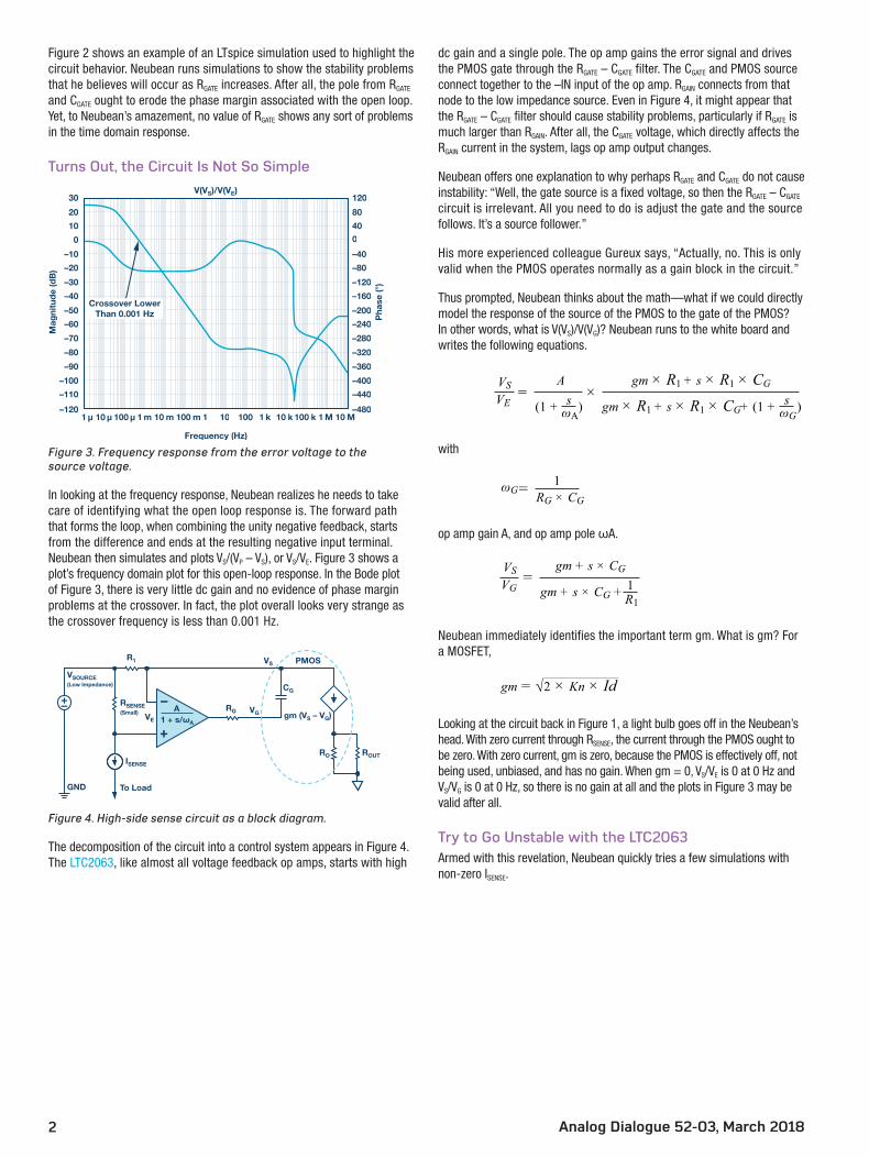
Figure 2 shows an example of an LTspice simulation used to highlight the circuit behavior. Neubean runs simulations to show the stability problems that he believes will occur as RGATE increases. After all, the pole from RGATE and CGATE ought to erode the phase margin associated with the open loop. Yet, to Neubean’s amazement, no value of RGATE shows any sort of problems in the time domain response.
Turns Out, the Circuit Is Not So Simple
Frequency (Hz)
1 µ 10 µ 100 µ 1 m 10 m 1 10 100 1 k 10 k 1 M 10 M100 k100 m–120
–110
–100
–90
–80
–70
–60
–50
–40
–30
–20
–10
0
10
20
30V(VS)/V(VE)
–480
–440
–400
–360
–320
–280
–240
–200
–160
–120
–80
–40
0
40
80
120
Mag
nitu
de
(dB
)
Pha
se (°
)
Crossover LowerThan 0.001 Hz
Figure 3. Frequency response from the error voltage to the source voltage.
In looking at the frequency response, Neubean realizes he needs to take care of identifying what the open loop response is. The forward path that forms the loop, when combining the unity negative feedback, starts from the difference and ends at the resulting negative input terminal. Neubean then simulates and plots VS/(VP – VS), or VS/VE. Figure 3 shows a plot’s frequency domain plot for this open-loop response. In the Bode plot of Figure 3, there is very little dc gain and no evidence of phase margin problems at the crossover. In fact, the plot overall looks very strange as the crossover frequency is less than 0.001 Hz.
VSOURCE(Low Impedance)
GND
A1 + s/ωA
ISENSE
To Load
RSENSE(Small)
R1
VE
RG
RO
gm (VS – VG)
ROUT
VG
PMOSVS
CG
Figure 4. High-side sense circuit as a block diagram.
The decomposition of the circuit into a control system appears in Figure 4. The LTC2063, like almost all voltage feedback op amps, starts with high
dc gain and a single pole. The op amp gains the error signal and drives the PMOS gate through the RGATE – CGATE filter. The CGATE and PMOS source connect together to the –IN input of the op amp. RGAIN connects from that node to the low impedance source. Even in Figure 4, it might appear that the RGATE – CGATE filter should cause stability problems, particularly if RGATE is much larger than RGAIN. After all, the CGATE voltage, which directly affects the RGAIN current in the system, lags op amp output changes.
Neubean offers one explanation to why perhaps RGATE and CGATE do not cause instability: “Well, the gate source is a fixed voltage, so then the RGATE – CGATE circuit is irrelevant. All you need to do is adjust the gate and the source follows. It’s a source follower.”
His more experienced colleague Gureux says, “Actually, no. This is only valid when the PMOS operates normally as a gain block in the circuit.”
Thus prompted, Neubean thinks about the math—what if we could directly model the response of the source of the PMOS to the gate of the PMOS? In other words, what is V(VS)/V(VG)? Neubean runs to the white board and writes the following equations.
= ×VSVE
AsωA
(1 +
gm × R1 + s × R1 × CG
gm × R1 + s × R1 × CGsωG
+ (1 + ))
with
= 1ωG RG × CG
op amp gain A, and op amp pole ωA.
=VSVG
gm + s × CG
1R1
gm + s × CG +
Neubean immediately identifies the important term gm. What is gm? For a MOSFET,
gm = 2 × Kn × Id √
Looking at the circuit back in Figure 1, a light bulb goes off in the Neubean’s head. With zero current through RSENSE, the current through the PMOS ought to be zero. With zero current, gm is zero, because the PMOS is effectively off, not being used, unbiased, and has no gain. When gm = 0, VS/VE is 0 at 0 Hz and VS/VG is 0 at 0 Hz, so there is no gain at all and the plots in Figure 3 may be valid after all.
Try to Go Unstable with the LTC2063Armed with this revelation, Neubean quickly tries a few simulations with non-zero ISENSE.

Analog Dialogue 52-03, March 2018 3
Frequency (Hz)
–80
–60
–40
–20
0
20
40
60
80
100
120
140
160
180
–440
–400
–360
–320
–280
–240
–200
–160
–120
–80
–40
0
40
80V(VS)/V(VE)
Mag
nitu
de
(dB
)
Pha
se (°
)
Crossover for1 MΩ, 100 kΩ, 100 Ω
1 µ 10 µ 100 µ 1 m 10 m 1 10 100 1 k 10 k 1 M 10 M100 k100 m
Figure 5. Frequency response from the error voltage to the source voltage, non-zero sense current.
Figure 5 shows what looks like a much more normal gain/phase plot of the response from VE to VS, crossing from >0 dB to <0 dB. Figure 5 should show about 2 kHz, with lots of PM at 100 Ω, a bit less PM at 100 kΩ, and even less with 1 MΩ, but not unstable.
Neubean goes to the lab and dials up a sense current with the high-side sense circuit LTC2063. He inserts a high RGATE value, first 100 kΩ and then 1 MΩ, expecting to see unstable behavior or at least some kind of ringing. Unfortunately, he does not.
He tries to increase the drain current in the MOSFET first by using more ISENSE and then by using a smaller RGAIN resistance. Nothing works to destabilize the circuit.
He returns to the simulation and tries to fill a phase margin with non-zero ISENSE. Even in simulation it seems difficult, if not impossible, to find instability or low phase margin.
Neubean finds Gureux and asks why he is failing to destabilize the circuit. Gureux advises him to do the numbers. Neubean is used to riddles from Gureux, so he examines what might be the actual pole associated with RGATE and the total gate capacitance. With 100 Ω and 250 pF, the pole is at 6.4 MHz; with 100 kΩ, the pole is at 6.4 kHz; and with 1 MΩ, the pole is at 640 Hz. The LTC2063 gain bandwidth product (GBP) is 20 kHz. When the LTC2063 takes gain, the closed-loop crossover frequency can easily slide below any effect of the RGATE – CGATE pole.
Yes, You Can Go UnstableRealizing that the op amp dynamics need to continue up into the range of the RGATE – CGATE pole, Neubean chooses a higher gain bandwidth product. The LTC6255 5 V op amp will directly fit into the circuit with a higher 6.5 MHz GBP.
Eagerly, Neubean tried a simulation with current, the LTC6255, 100 kΩ gate resistance, and with 300 mA sense current.
Neubean then proceeds to add RGATE in simulation. With enough RGATE, an extra pole can destabilize a circuit.
Time (ms)
219.
6
219.
7
219.
8
219.
9
220.
0
220.
2
220.
3
220.
4
220.
5
220.
6
220.
7
220.
8
229.
0
221.
0
220.
1
–0.4
0.0
0.4
0.8
1.2
1.6
2.0
2.4
2.8
3.2
3.6
4.0
4.4V(VOUT) V(VG)
Vo
ltag
e O
vers
win
g (V
)
300 mASense Current 0 Sense Current
Figure 6. A time domain plot with ringing.
Frequency (Hz)
10 100 100 k1 k 10 k 1 M 10 M–80
–60
–40
–20
0
20
40
60
80
100
–270
–240
–210
–180
–150
–120
–90
–60
–30
0V(VS)/V(VE)
Mag
nitu
de
(dB
)
Pha
se (°
)
Essentially No Phase Margin
Figure 7. A normal Bode plot once we add current, VE to VS, with terrible phase margin.
Figure 6 and Figure 7 show simulation results with high RGATE values. At a constant 300 mA sense current, this simulation shows instability.
Lab ResultsWanting to see if the circuit might act badly while sensing a non-zero current, Neubean tries the LTC6255 with a step changing load current and uses three different RGATE values. ISENSE transitions from a base of 60 mA to a higher value of 220 mA enabled by a momentary switch that brings in more parallel load resistance. There is no zero ISENSE measurement, because it is already shown that the MOSFET gain is too low in that case.
Indeed, Figure 8 finally shows truly compromised stability with 100 kΩ and 1 MΩ resistors. Because the output voltage is heavily filtered, the gate voltage becomes the detector for ringing. Ringing denotes poor or negative phase margin, and ringing frequency indicates crossover frequency.

Analog Dialogue 52-03, March 20184
Time (µs)
–80.6 19.4 419.4319.4219.4119.4–2.0
–1.6
2.0
1.6
1.2
0.8
0.4
0.0
–0.4
–0.8
–1.2
No
rmal
ized
Gat
e V
olt
age
(V)
Figure 8. RGATE = 100 Ω, current from low to high transient.
Time (µs)
–91.3 8.7 408.7308.7208.7108.7–2.0
–1.6
2.0
1.6
1.2
0.8
0.4
0.0
–0.4
–0.8
–1.2
No
rmal
ized
Gat
e V
olt
age
(V)
Figure 9. RGATE = 100 Ω, current from high to low transient.
Time (µs)
–78.0 22.0 422.0322.0220.0122.0–2.0
–1.6
2.0
1.6
1.2
0.8
0.4
0.0
–0.4
–0.8
–1.2
No
rmal
ized
Gat
e V
olt
age
(V)
Figure 10. RGATE = 100 kΩ, current from low to high transient.
Time (µs)
–78.0 22.0 422.0322.0220.0122.0–2.0
–1.6
2.0
1.6
1.2
0.8
0.4
0.0
–0.4
–0.8
–1.2
No
rmal
ized
Gat
e V
olt
age
(V)
Figure 11. RGATE = 100 kΩ, current from high to low transient.
Time (µs)
–0.3 0.1 1.71.30.90.5–2.0
–1.6
2.0
1.6
1.2
0.8
0.4
0.0
–0.4
–0.8
–1.2
No
rmal
ized
Gat
e V
olt
age
(V)
Figure 12. RGATE = 1 MΩ, current from low to high transient.
Time (µs)
–0.3 0.1 1.71.30.90.5–2.0
–1.6
2.0
1.6
1.2
0.8
0.4
0.0
–0.4
–0.8
–1.2
No
rmal
ized
Gat
e V
olt
age
(V)
Figure 13. RGATE = 1 MΩ, current from high to low transient.

Analog Dialogue 52-03, March 2018 5
A Moment to BrainstormNeubean realizes that he has seen many high-side integrated current sense circuits and, unfortunately, there is no chance for an engineer to decide on gate resistance, because everything is inside the part. Examples that came to his mind were AD8212, LTC6101, LTC6102, and LTC6104 high voltage, high-side current sense devices. In fact, the AD8212 uses a PNP transistor rather than a PMOS FET. He tells Gureux, “Eh, it doesn’t really matter, because modern devices already solve this problem.”
As though expecting this comment, almost cutting off Neubean before his last word, the professor responds: “Let’s say you want a combination of extremely low supply current and zero-drift input offset, such as in a remotely located battery-powered instrument. You might want an LTC2063 or LTC2066 as the primary amplifier. Or, perhaps, you need to measure a low level current level perhaps through a 470 Ω shunt as accurately and noiselessly as possible; in that case you might want to use the ADA4528, which has rail-to-rail input capability. In these cases you will need to deal with the MOSFET drive circuitry.”
And So …Clearly, then, it is possible to destabilize the high-side current sense circuit by using too large of a gate resistor. Neubean relates this finding to his willing teacher Gureux. Gureux notes that RGATE can in fact destabilize the circuit, but the initial inability to find this behavior drew from a wrongly formulated problem. There needed to be gain, which in this circuit required there to be non-zero signal being measured.
Gureux replies, “Sure, when a pole erodes the phase margin at a crossover, ringing happens. But your 1 MΩ of added gate resistance is absurd—even 100 kΩ is crazy. Remember, it is always good to try to limit the output current of an op amp in case it tries to swing a gate capacitance from one rail to another rail.”
Neubean agrees. “So what value of resistance do I use?”
Gureux notes confidently, “100 Ω.”
Aaron Schultz [[email protected]] is an applications engineering manager in the LPS business unit. His multiple system engineering roles in both design and applications have exposed him to topics ranging across battery management, photovoltaics, dimmable LED drive circuits, low voltage and high current dc-to-dc conversion, high speed fiber optic communication, advanced DDR3 memory R&D, custom tool development, validation, and basic analog circuits, while over half of his career has been spent in power conver-sion. He graduated from Carnegie Mellon University in 1993 and MIT in 1995. By night he plays jazz piano.
Aaron Schultz