Embed Size (px)
Citation preview
Cin
zia
Da
Vià
, T
he U
nive
rsit
y of
Man
chest
er,
UK
– R
D S
ens
ors
and M
icro
Fab
Sys
tem
s 12
th J
une 2
013
RD Collaboration on 3D Sensors and Micro-Fabricated Systems
Introduction Objectives State of the art Challenges Synergies Deliverables and Milestones Organization Collaboration Summary
Cinzia Da Vià, the University of Manchester, UK
Cin
zia
Da
Vià
, T
he U
nive
rsit
y of
Man
chest
er,
UK
– R
D S
ens
ors
and M
icro
Fab
Sys
tem
s 12
th J
une 2
013
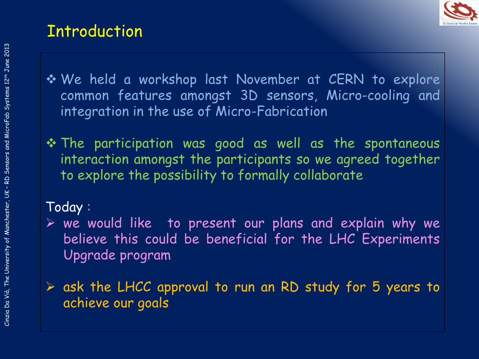
We held a workshop last November at CERN to explore
common features amongst 3D sensors, Micro-cooling and integration in the use of Micro-Fabrication
The participation was good as well as the spontaneous
interaction amongst the participants so we agreed together to explore the possibility to formally collaborate
Today : we would like to present our plans and explain why we
believe this could be beneficial for the LHC Experiments Upgrade program
ask the LHCC approval to run an RD study for 5 years to
achieve our goals
Introduction
Cin
zia
Da
Vià
, T
he U
nive
rsit
y of
Man
chest
er,
UK
– R
D S
ens
ors
and M
icro
Fab
Sys
tem
s 12
th J
une 2
013
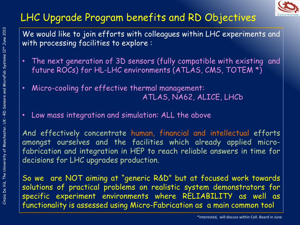
LHC Upgrade Program benefits and RD Objectives
We would like to join efforts with colleagues within LHC experiments and with processing facilities to explore : • The next generation of 3D sensors (fully compatible with existing and
future ROCs) for HL-LHC environments (ATLAS, CMS, TOTEM *)
• Micro-cooling for effective thermal management: ATLAS, NA62, ALICE, LHCb
• Low mass integration and simulation: ALL the above And effectively concentrate human, financial and intellectual efforts amongst ourselves and the facilities which already applied micro-fabrication and integration in HEP to reach reliable answers in time for decisions for LHC upgrades production. So we are NOT aiming at “generic R&D” but at focused work towards solutions of practical problems on realistic system demonstrators for specific experiment environments where RELIABILITY as well as functionality is assessed using Micro-Fabrication as a main common tool
*interested, will discuss within Coll. Board in June
Cin
zia
Da
Vià
, T
he U
nive
rsit
y of
Man
chest
er,
UK
– R
D S
ens
ors
and M
icro
Fab
Sys
tem
s 12
th J
une 2
013
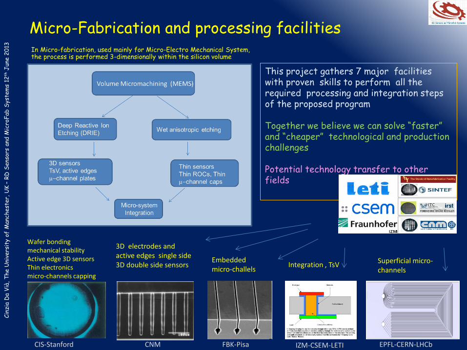
Micro-Fabrication and processing facilities
Wafer bonding mechanical stability Active edge 3D sensors Thin electronics micro-channels capping
3D electrodes and active edges single side 3D double side sensors
Embedded micro-challels
Integration , TsV Superficial micro- channels
This project gathers 7 major facilities with proven skills to perform all the required processing and integration steps of the proposed program Together we believe we can solve “faster” and “cheaper” technological and production challenges Potential technology transfer to other fields
CIS-Stanford CNM FBK-Pisa IZM-CSEM-LETI EPFL-CERN-LHCb
In Micro-fabrication, used mainly for Micro-Electro Mechanical System, the process is performed 3-dimensionally within the silicon volume
Cin
zia
Da
Vià
, T
he U
nive
rsit
y of
Man
chest
er,
UK
– R
D S
ens
ors
and M
icro
Fab
Sys
tem
s 12
th J
une 2
013
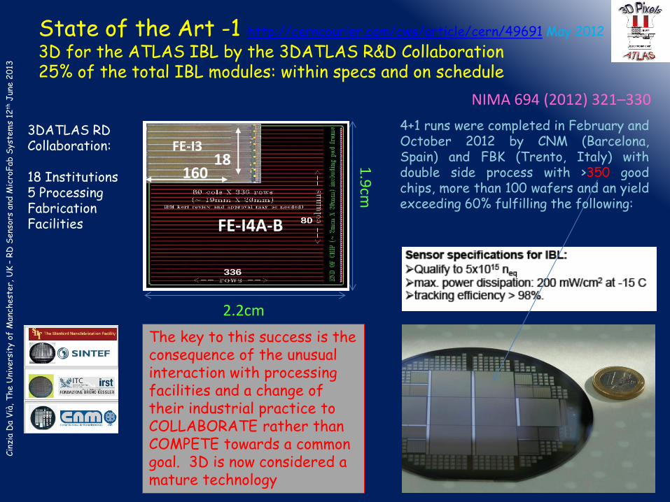
State of the Art -1 http://cerncourier.com/cws/article/cern/49691 May 2012
3D for the ATLAS IBL by the 3DATLAS R&D Collaboration 25% of the total IBL modules: within specs and on schedule
160 18
FE-I3
FE-I4A-B
3DATLAS RD Collaboration: 18 Institutions 5 Processing Fabrication Facilities
4+1 runs were completed in February and October 2012 by CNM (Barcelona, Spain) and FBK (Trento, Italy) with double side process with >350 good chips, more than 100 wafers and an yield exceeding 60% fulfilling the following:
NIMA 694 (2012) 321–330
2.2cm 1
.9cm
The key to this success is the consequence of the unusual interaction with processing facilities and a change of their industrial practice to COLLABORATE rather than COMPETE towards a common goal. 3D is now considered a mature technology
Cin
zia
Da
Vià
, T
he U
nive
rsit
y of
Man
chest
er,
UK
– R
D S
ens
ors
and M
icro
Fab
Sys
tem
s 12
th J
une 2
013
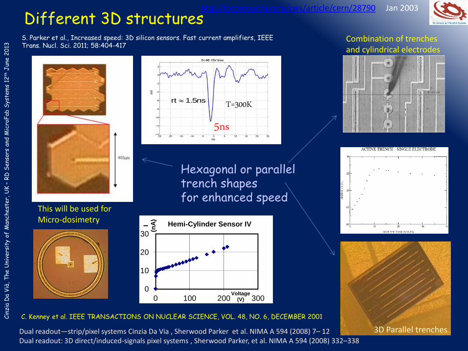
Different 3D structures
5ns T=300K rt 1.5ns
0
10
20
30
0 100 200 300
I
(nA
)
Voltage (V)
Hemi-Cylinder Sensor IV
Hexagonal or parallel trench shapes for enhanced speed
3D Parallel trenches
This will be used for Micro-dosimetry
C. Kenney et al. IEEE TRANSACTIONS ON NUCLEAR SCIENCE, VOL. 48, NO. 6, DECEMBER 2001
Combination of trenches and cylindrical electrodes
S. Parker et al., Increased speed: 3D silicon sensors. Fast current amplifiers, IEEE Trans. Nucl. Sci. 2011; 58:404-417
http://cerncourier.com/cws/article/cern/28790 Jan 2003
Dual readout—strip/pixel systems Cinzia Da Via , Sherwood Parker et al. NIMA A 594 (2008) 7– 12 Dual readout: 3D direct/induced-signals pixel systems , Sherwood Parker, et al. NIMA A 594 (2008) 332–338

Cin
zia
Da
Vià
, T
he U
nive
rsit
y of
Man
chest
er,
UK
– R
D S
ens
ors
and M
icro
Fab
Sys
tem
s 12
th J
une 2
013
Explored since a while in microprocessor
industry
Cooling channel is integrated in the substrate:
Can customize the routing of channels to run exactly under the heat sources.
Many parallel channels: large liquid-to-substrate heat exchange
surface.
Low mass : No extra ‘bulky’ thermal interface required
between cooling channel and substrate.
No heat flows in the substrate plane: Small thermal gradients across the module.
All material is silicon : No mechanical stress due to CTE mismatch.
State of the Art-2 Micro-cooling
Copyright 2013 CSEM | Div C | A.Pezous| Page 7
• Cooling device based on the ATLAS design
• Pressure tests > 100bar
LHCb system layout. J. Buytaert, Pixel2012
Pioneering work for HEP within CERN PH-DT

Cin
zia
Da
Vià
, T
he U
nive
rsit
y of
Man
chest
er,
UK
– R
D S
ens
ors
and M
icro
Fab
Sys
tem
s 12
th J
une 2
013
Slide courtesy of Jan Buytaert LHCb
Pioneering experiments using micro-cooling in collaboration with CERN PH-DT use C6F14 and C4F10
with less aggressive geometrical constraints
Decision taken to use u-channels in experiment!
Cin
zia
Da
Vià
, T
he U
nive
rsit
y of
Man
chest
er,
UK
– R
D S
ens
ors
and M
icro
Fab
Sys
tem
s 12
th J
une 2
013
15
0-2
00
mm
Afte
r backth
inn
ing
3D
50
-10
0 m
m
3D
thickn
ess
~50
mm
cap
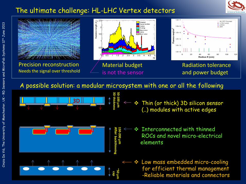
Thin (or thick) 3D silicon sensor
(..) modules with active edges
Interconnected with thinned ROCs and novel micro-electrical
elements Low mass embedded micro-cooling for efficient thermal management -Reliable materials and connectors
Precision reconstruction Needs the signal over threshold
Material budget is not the sensor
Radiation tolerance and power budget
The ultimate challenge: HL-LHC Vertex detectors
A possible solution: a modular microsystem with one or all the following
Cin
zia
Da
Vià
, T
he U
nive
rsit
y of
Man
chest
er,
UK
– R
D S
ens
ors
and M
icro
Fab
Sys
tem
s 12
th J
une 2
013
0
5000
10000
15000
20000
25000
0 5 1015
1 1016
1.5 1016
DIAMOND NIMA 565 (2006)278-283
Pixel CMS NIMA 552(2005)232-238
ATLAS-strips IEEE TNS 52(2005) 1903
SPI-75mm NIMA (2005) 212-219
3D-4E C. Da Viá et al. July 2007
3D-3E C. Da Viá et al.July 2007
3D-4E C. Da Via et al. July 2007
Sig
nal ch
arg
e [
e-]
Fluence [n/cm2]
0 8 1015
1.6 1016
2.4 1016
Fluence [p/cm2]
C. Da Via'/ July 07
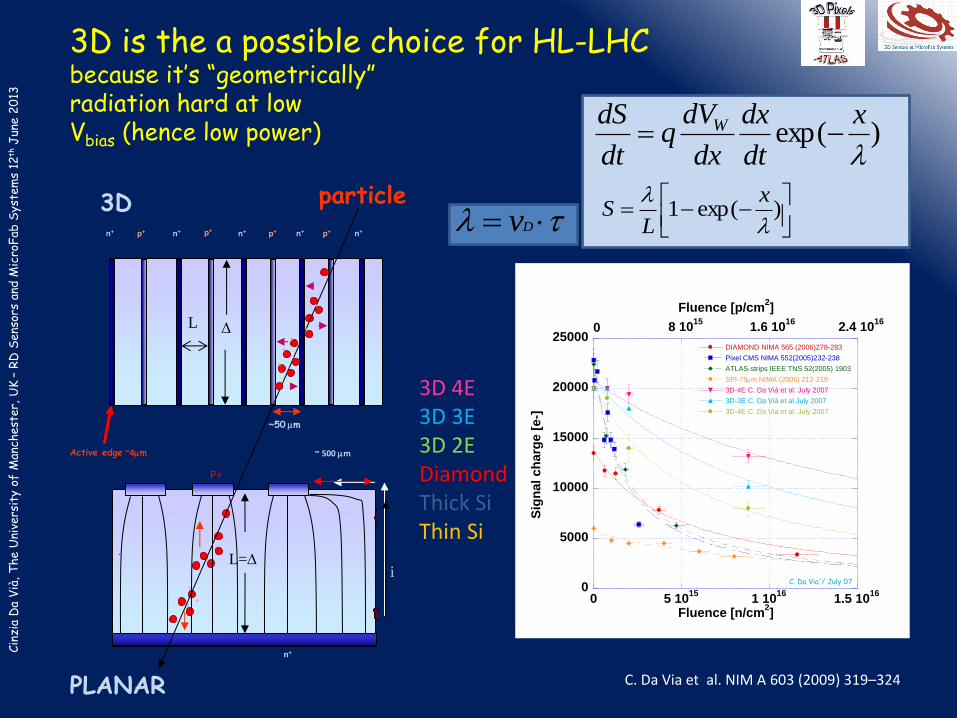
3D is the a possible choice for HL-LHC because it’s “geometrically” radiation hard at low Vbias (hence low power)
particle
PLANAR
~ 500 mm
-
P+
n+
-
+
+ +
L=D i
Active edge ~4mm
~50 mm
3D n+ p+ n+ n+ n+ p+ p+ p+ n+
-
-
-
-
+
+
+
+
+
L D
)exp(
x
dt
dx
dx
dVq
dt
dS W
)exp(1
x
LS Dv
C. Da Via et al. NIM A 603 (2009) 319–324
3D 4E 3D 3E 3D 2E Diamond Thick Si Thin Si
Cin
zia
Da
Vià
, T
he U
nive
rsit
y of
Man
chest
er,
UK
– R
D S
ens
ors
and M
icro
Fab
Sys
tem
s 12
th J
une 2
013
2E = 103um 3E= 71um (IBL DESIGN) 4E= 56um HL 5E= 47um
0
20
40
60
80
100
120
0 2 1015
4 1015
6 1015
8 1015
1 1016
Sig
nal
eff
icie
nc
y [%
]
Fluence [n/cm2]
2E
C. Da Viá July 07
0
20
40
60
80
100
120
0 2 1015
4 1015
6 1015
8 1015
1 1016
Sig
nal eff
icie
ncy [%
]
Fluence [n/cm2]
3E
C. Da Viá July 07 0
20
40
60
80
100
120
0 2 1015
4 1015
6 1015
8 1015
1 1016
Sig
na
l e
ffic
ien
cy
[%
]
Fluence [n/cm2]
4E
C. Da Viá et al. July 07
0
20
40
60
80
100
120
0 50 100 150 200 250 300
8.8E15
Sig
na
l E
ffic
ien
cy [
%]
Inter-electrode spacing [mm]
C. Da Via' April 08
L=IES [um] 105 71-IBL 56-HL 47
Signal Efficiency [%] 45 51 66 68
Charge 50um [e-] 1800 2040 2640 2720
Charge 100um [e-] 3200 4080 5280 5440
Charge 200um[e-] 6400 8160 10560 10880
At 9x10¹⁵ ncm -2 And biases below 200V
How much signal for 3D at HL-LHC fluences?
)exp(1
L
LS x v
Drift length
Trapping time
Drift Velocity (saturated)
L= Inter-Electrode Spacing
Nucl. Instrum. Meth. A 603 (2009) 319–324
V=100V
Cin
zia
Da
Vià
, T
he U
nive
rsit
y of
Man
chest
er,
UK
– R
D S
ens
ors
and M
icro
Fab
Sys
tem
s 12
th J
une 2
013
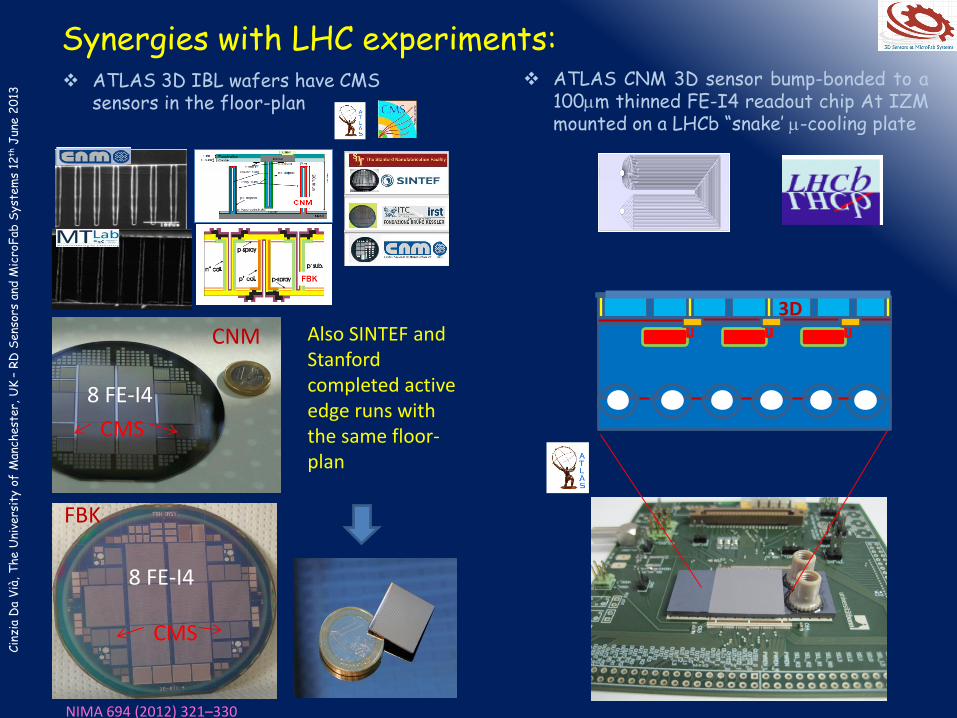
Synergies with LHC experiments:
NIMA 694 (2012) 321–330
Also SINTEF and Stanford completed active edge runs with the same floor-plan
FBK
8 FE-I4
CMS
CNM
8 FE-I4
CMS
ATLAS 3D IBL wafers have CMS sensors in the floor-plan
3D
ATLAS CNM 3D sensor bump-bonded to a 100mm thinned FE-I4 readout chip At IZM mounted on a LHCb “snake’ m-cooling plate
Cin
zia
Da
Vià
, T
he U
nive
rsit
y of
Man
chest
er,
UK
– R
D S
ens
ors
and M
icro
Fab
Sys
tem
s 12
th J
une 2
013
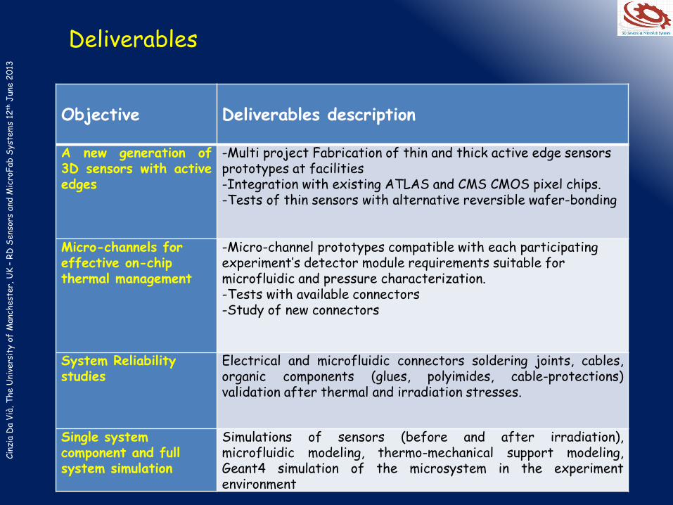
Deliverables
Objective
Deliverables description
A new generation of 3D sensors with active edges
-Multi project Fabrication of thin and thick active edge sensors prototypes at facilities -Integration with existing ATLAS and CMS CMOS pixel chips. -Tests of thin sensors with alternative reversible wafer-bonding
Micro-channels for effective on-chip thermal management
-Micro-channel prototypes compatible with each participating experiment’s detector module requirements suitable for microfluidic and pressure characterization. -Tests with available connectors -Study of new connectors
System Reliability studies
Electrical and microfluidic connectors soldering joints, cables, organic components (glues, polyimides, cable-protections) validation after thermal and irradiation stresses.
Single system component and full system simulation
Simulations of sensors (before and after irradiation), microfluidic modeling, thermo-mechanical support modeling, Geant4 simulation of the microsystem in the experiment environment
Cin
zia
Da
Vià
, T
he U
nive
rsit
y of
Man
chest
er,
UK
– R
D S
ens
ors
and M
icro
Fab
Sys
tem
s 12
th J
une 2
013
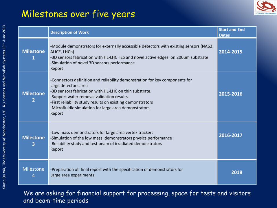
Milestones over five years
Description of Work Start and End Dates
Milestone 1
-Module demonstrators for externally accessible detectors with existing sensors (NA62, ALICE, LHCb) -3D sensors fabrication with HL-LHC IES and novel active edges on 200um substrate -Simulation of novel 3D sensors performance Report
2014-2015
Milestone 2
-Connectors definition and reliability demonstration for key components for large detectors area -3D sensors fabrication with HL-LHC on thin substrate. -Support wafer removal validation results -First reliability study results on existing demonstrators -Microfluidic simulation for large area demonstrators Report
2015-2016
Milestone 3
-Low mass demonstrators for large area vertex trackers -Simulation of the low mass demonstrators physics performance -Reliability study and test beam of irradiated demonstrators Report
2016-2017
Milestone 4
-Preparation of final report with the specification of demonstrators for Large area experiments
2018
We are asking for financial support for processing, space for tests and visitors and beam-time periods
Cin
zia
Da
Vià
, T
he U
nive
rsit
y of
Man
chest
er,
UK
– R
D S
ens
ors
and M
icro
Fab
Sys
tem
s 12
th J
une 2
013
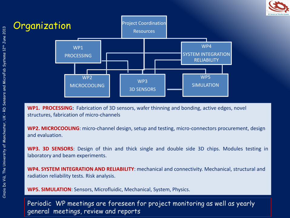
Organization
WP1. PROCESSING: Fabrication of 3D sensors, wafer thinning and bonding, active edges, novel structures, fabrication of micro-channels WP2. MICROCOOLING: micro-channel design, setup and testing, micro-connectors procurement, design and evaluation. WP3. 3D SENSORS: Design of thin and thick single and double side 3D chips. Modules testing in laboratory and beam experiments. WP4. SYSTEM INTEGRATION AND RELIABILITY: mechanical and connectivity. Mechanical, structural and radiation reliability tests. Risk analysis. WP5. SIMULATION: Sensors, Microfluidic, Mechanical, System, Physics.
Project Coordination
Resources
WP1
PROCESSING
WP2
MICROCOOLING
WP3
3D SENSORS
WP4
SYSTEM INTEGRATION RELIABILITY
WP5
SIMULATION
Periodic WP meetings are foreseen for project monitoring as well as yearly general meetings, review and reports

Cin
zia
Da
Vià
, T
he U
nive
rsit
y of
Man
chest
er,
UK
– R
D S
ens
ors
and M
icro
Fab
Sys
tem
s 12
th J
une 2
013
Collaboration
Institutes 1. Bergen (Heidi Sandaker, Bjarne Stugu) (ATLAS) 2. Bari (Vito Manzari, Giuseppe Eguenio Bruno, Cosimo Pastore) (ALICE) 3. Cosenza (Anna Mastroberardino, Giuseppe Cocorullo, Felice Crupi, Marco
Schioppa, GianCarlo Susinno) 4. Glasgow (Richard Bates) (ATLAS) 5. Gottingen (Jens Weingarten, Arnulf Quadt, Joern Grosse-Knetter, Julia Rieger)
(ATLAS) 6. Hawaii (Sherwood Parker) (ATLAS) 7. IFAE Barcelona (Sebastian Grinstein, Andrea Micelli, Ivan Lopez) (ATLAS) 8. Manchester (C. Da Vià, Chris Parkes, Joleen Pater, Vladislav Tyzhnevyi; Stefano Di
Capua, Steve Watts) (ATLAS, LHCb) 9. MPI Munich (H-G Moser) Late expression 10. Oslo (Ole Rohne) (ATLAS) 11. Oxford (Malcolm John) (LHCb) 12. Prague (Stanislav Pospisil, Tomas Slavicek) (ATLAS) 13. Purdue (Daniela Bortoletto, Mayur Bubna, Alex Krzywda, Mayra Cervantes,
Richard Brosius, Gino Bolla, Petra Merkel, Ian Shipsey, Kaushik Roy) (CMS) 14. Seattle (Washington Uni) (Shih-Chieh Hsu) ATLAS 15. SLAC (Chris Kenney, Philippe Grenier, Jasmine Hasi, Dong Su) (ATLAS) 16. Stony Brook (Dmitri Tsibichev) (ATLAS) 17. Torino (Flavio Marchetto, Nicolo Cartiglia, Roberta Arcidiacono) (NA62), 18. Trento (GianFranco Dalla Betta, Lucio Pancheri, Marco Povoli, Roberto Mendicino,
Alberto Quaranta) 19. Udine (Mario Paolo Giordani, Marina Cobal)
Processing Facilities CNM (Giulio Pellegrini, Manuel Lozano, Celeste Fleta, Miguel Ullan, Salvador Hidalgo, Virginia Greco, David Quirion), Barcelona, Spain FBK (Maurizio Boscardin, Alvise Bagolini, Francesca Mattedi, Sabina Ronchin, Pierluigi Bellutti, Paolo Conci, Stefano Girardi, Nicola Zorzi, Gabriele Giacomini, Claudio Piemonte) CSEM (Aurelie Pezous, Patrick Albert, Olivier Dubochet) , SINTEF (Angela Kok, Thor-Erik Hansen) IZM (Thomas Fritszch, Oswin Erhmann) CEA-LETI (Eric Rouchouze, Jean Francois Tessier, Yann Lamy), NSF/SLAC (Chris Kenney, Jasmine Hasi) Stanford Nano Fabrication Facility, Palo Alto California USA More groups have expressed interest to join .
Their request will be considered later this year if the proposal will receive positive recommendation by this committee
Cin
zia
Da
Vià
, T
he U
nive
rsit
y of
Man
chest
er,
UK
– R
D S
ens
ors
and M
icro
Fab
Sys
tem
s 12
th J
une 2
013
Summary
In this RD collaboration we would like to join efforts and skills to solve problems for HL-
LHC experiments upgrades using micro-fabrication We aim to build demonstrators for relevant testing at future realistic experimental
conditions by a dedicated and not a generic work activity
Seven Top Processing Facilities joined the project: this has proven to be the key for a rapid solution of technological problems
Several groups and facilities in this proposal have industrialized 3D sensors and had them included in the first detector upgrade at the LHC, the ATLAS IBL, after a stringent review process. Thanks to that 3D is now considered a ‘mature’ technology and being considered for pixel upgrades in various experiments.
We are therefore asking this committee to give this collaboration an opportunity to capitalize on this experience so this sensor technology can be brought to the next level. Together with micro-system prototypes we aim at gathering the relevant reliability and production information in time for decisions at experiments We believe that having this done as a CERN RD is the best platform to unify effort amongst and for CERN-LHC experiments