Embed Size (px)
Citation preview
CMB-S4 Collaboration Meeting, March 8-12, 2021
Readout Preliminary Baseline Design Overview
Zeesh Ahmed (L2 scientist) for WBS 1.04 Plenary Session, Tuesday, March 9, 2021
CMB-S4 Collaboration Meeting, March 8-12, 2021
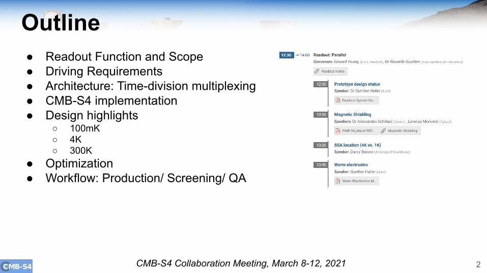
● Readout Function and Scope● Driving Requirements● Architecture: Time-division multiplexing● CMB-S4 implementation● Design highlights
○ 100mK○ 4K○ 300K
● Optimization● Workflow: Production/ Screening/ QA
2
Outline
CMB-S4 Collaboration Meeting, March 8-12, 2021 3
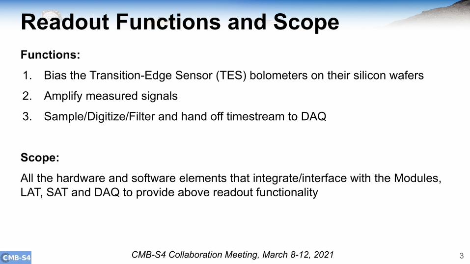
Readout Functions and ScopeFunctions:
1. Bias the Transition-Edge Sensor (TES) bolometers on their silicon wafers
2. Amplify measured signals
3. Sample/Digitize/Filter and hand off timestream to DAQ
Scope:
All the hardware and software elements that integrate/interface with the Modules, LAT, SAT and DAQ to provide above readout functionality
CMB-S4 Collaboration Meeting, March 8-12, 2021 4
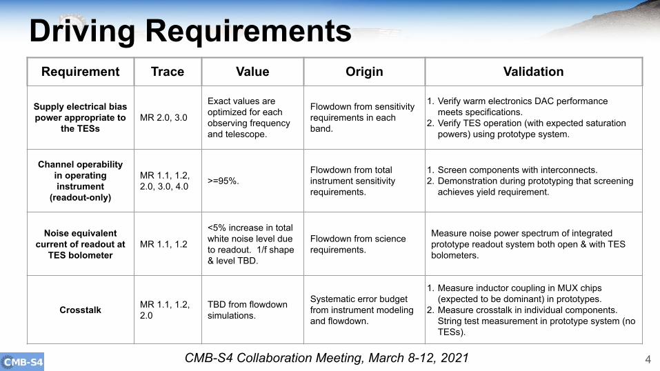
Driving RequirementsRequirement Trace Value Origin Validation
Supply electrical bias power appropriate to
the TESsMR 2.0, 3.0
Exact values are optimized for each observing frequency and telescope.
Flowdown from sensitivity requirements in each band.
1. Verify warm electronics DAC performance meets specifications.
2. Verify TES operation (with expected saturation powers) using prototype system.
Channel operability in operating instrument
(readout-only)
MR 1.1, 1.2, 2.0, 3.0, 4.0 >=95%.
Flowdown from total instrument sensitivity requirements.
1. Screen components with interconnects.2. Demonstration during prototyping that screening
achieves yield requirement.
Noise equivalent current of readout at
TES bolometer MR 1.1, 1.2
<5% increase in total white noise level due to readout. 1/f shape & level TBD.
Flowdown from science requirements.
Measure noise power spectrum of integrated prototype readout system both open & with TES bolometers.
Crosstalk MR 1.1, 1.2, 2.0
TBD from flowdown simulations.
Systematic error budget from instrument modeling and flowdown.
1. Measure inductor coupling in MUX chips (expected to be dominant) in prototypes.
2. Measure crosstalk in individual components. String test measurement in prototype system (no TESs).
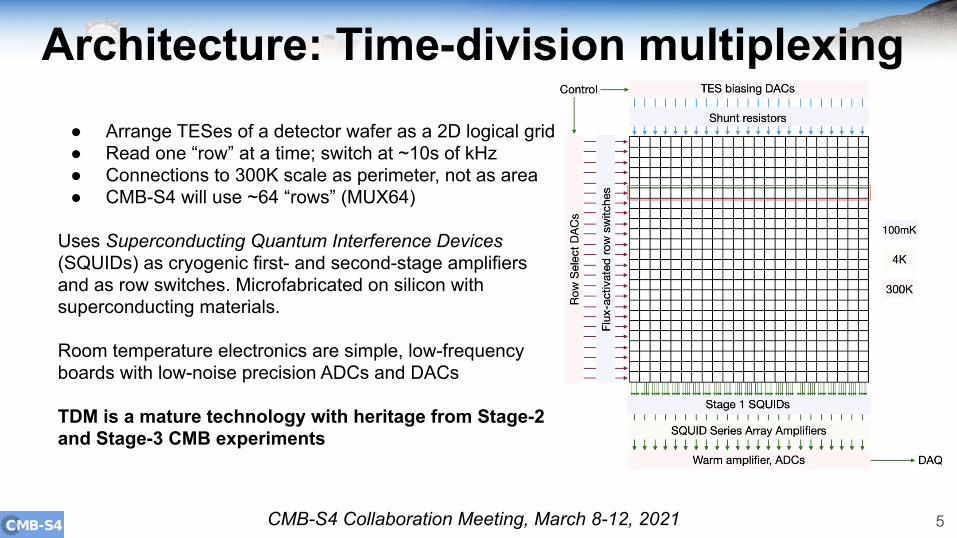
CMB-S4 Collaboration Meeting, March 8-12, 2021 5
Architecture: Time-division multiplexing ● Arrange TESes of a detector wafer as a 2D logical grid● Read one “row” at a time; switch at ~10s of kHz● Connections to 300K scale as perimeter, not as area● CMB-S4 will use ~64 “rows” (MUX64)
Uses Superconducting Quantum Interference Devices (SQUIDs) as cryogenic first- and second-stage amplifiers and as row switches. Microfabricated on silicon with superconducting materials.
Room temperature electronics are simple, low-frequency boards with low-noise precision ADCs and DACs
TDM is a mature technology with heritage from Stage-2 and Stage-3 CMB experiments
CMB-S4 Collaboration Meeting, March 8-12, 2021
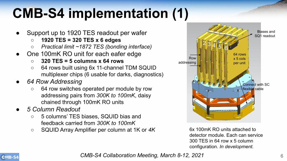
● Support up to 1920 TES readout per wafer○ 1920 TES = 320 TES x 6 edges○ Practical limit ~1872 TES (bonding interface)
● One 100mK RO unit for each eafer edge○ 320 TES = 5 columns x 64 rows○ 64 rows built using 6x 11-channel TDM SQUID
multiplexer chips (6 usable for darks, diagnostics)● 64 Row Addressing
○ 64 row switches operated per module by row addressing pairs from 300K to 100mK, daisy chained through 100mK RO units
● 5 Column Readout○ 5 columns’ TES biases, SQUID bias and
feedback carried from 300K to 100mK○ SQUID Array Amplifier per column at 1K or 4K
6
CMB-S4 implementation (1)
6x 100mK RO units attached to detector module. Each can service 300 TES in 64 row x 5 column configuration. In development.
1 2 3 4 5 664 rows x 5 cols per unit
Connect with SC flexible cable
Row addressing
Biases and SQ1 readout
CMB-S4 Collaboration Meeting, March 8-12, 2021
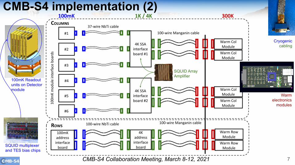
Warm Row Module
#1
#2
#3
#4
#5
100mK address
interface board
4K address
interface board
#6
4K SSA interface board #1
4K SSA interface board #2
100-wire Manganin cable
37-wire NbTi cable
100-wire NbTi cable
100m
K m
od
ule
inte
rfac
e b
oar
ds
100mK 1K / 4K 300K
100-wire Manganin cable
Warm Row Module
Warm Col Module
Warm Col Module
Warm Col Module
Warm Col Module
COLUMNS
ROWS
7
SQUID multiplexer and TES bias chips
100mK Readout units on Detector module
SQUID Array Amplifier
Warm electronics
modules
Cryogenic cabling
CMB-S4 implementation (2)
CMB-S4 Collaboration Meeting, March 8-12, 2021 8
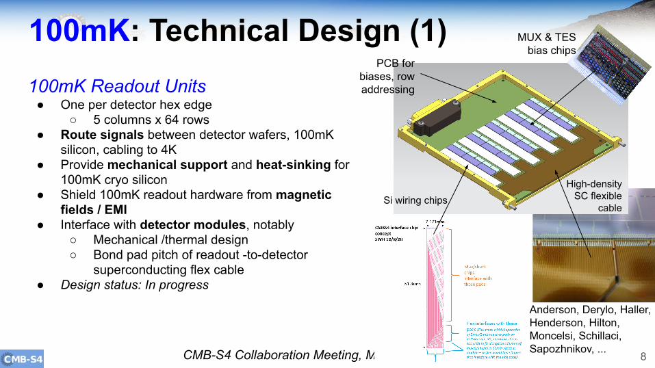
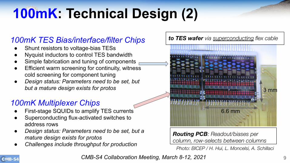
100mK: Technical Design (1)100mK Readout Units
● One per detector hex edge○ 5 columns x 64 rows
● Route signals between detector wafers, 100mK silicon, cabling to 4K
● Provide mechanical support and heat-sinking for 100mK cryo silicon
● Shield 100mK readout hardware from magnetic fields / EMI
● Interface with detector modules, notably○ Mechanical /thermal design○ Bond pad pitch of readout -to-detector
superconducting flex cable● Design status: In progress
Anderson, Derylo, Haller, Henderson, Hilton, Moncelsi, Schillaci, Sapozhnikov, ...
MUX & TES bias chips
High-density SC flexible
cableSi wiring chips
PCB for biases, row addressing
CMB-S4 Collaboration Meeting, March 8-12, 2021
100mK TES Bias/interface/filter Chips● Shunt resistors to voltage-bias TESs● Nyquist inductors to control TES bandwidth● Simple fabrication and tuning of components● Efficient warm screening for continuity, witness
cold screening for component tuning● Design status: Parameters need to be set, but
but a mature design exists for protos
100mK Multiplexer Chips● First-stage SQUIDs to amplify TES currents● Superconducting flux-activated switches to
address rows● Design status: Parameters need to be set, but a
mature design exists for protos● Challenges include throughput for production
9
to TES wafer via superconducting flex cable
Photo: BICEP / H. Hui, L. Moncelsi, A. Schillaci
Routing PCB: Readout/biases per column, row-selects between columns
100mK: Technical Design (2)
6.6 mm
3 mm
CMB-S4 Collaboration Meeting, March 8-12, 2021
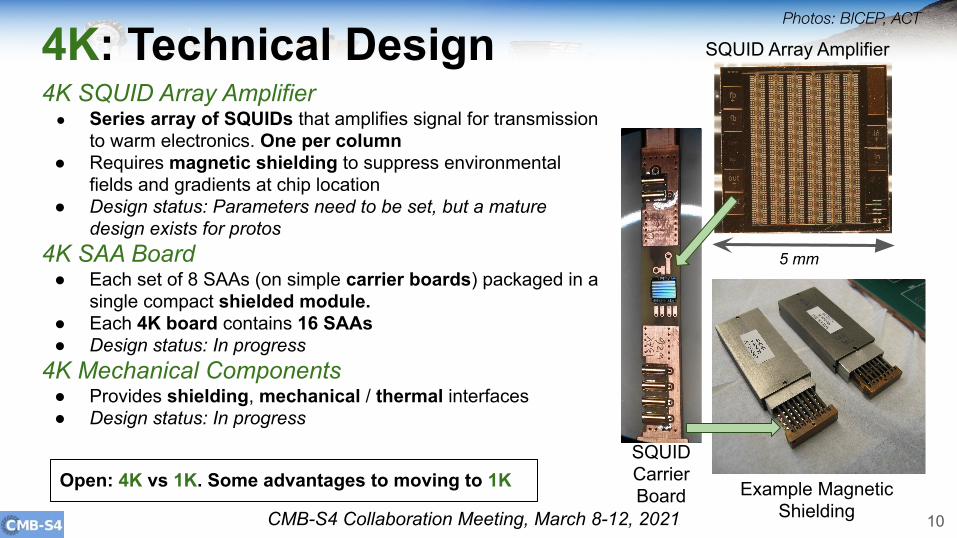
4K: Technical Design 4K SQUID Array Amplifier
● Series array of SQUIDs that amplifies signal for transmission to warm electronics. One per column
● Requires magnetic shielding to suppress environmental fields and gradients at chip location
● Design status: Parameters need to be set, but a mature design exists for protos
4K SAA Board● Each set of 8 SAAs (on simple carrier boards) packaged in a
single compact shielded module. ● Each 4K board contains 16 SAAs ● Design status: In progress
4K Mechanical Components● Provides shielding, mechanical / thermal interfaces● Design status: In progress
10
5 mm
SQUID Array Amplifier
SQUID Carrier Board Example Magnetic
ShieldingOpen: 4K vs 1K. Some advantages to moving to 1K
Photos: BICEP, ACT
CMB-S4 Collaboration Meeting, March 8-12, 2021
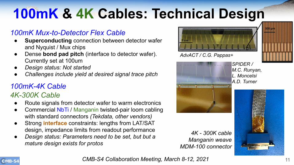
100mK & 4K Cables: Technical Design 100mK Mux-to-Detector Flex Cable
● Superconducting connection between detector wafer and Nyquist / Mux chips
● Dense bond pad pitch (interface to detector wafer). Currently set at 100um
● Design status: Not started ● Challenges include yield at desired signal trace pitch
100mK-4K Cable4K-300K Cable
● Route signals from detector wafer to warm electronics● Commercial NbTi / Manganin twisted-pair loom cabling
with standard connectors (Tekdata, other vendors)● Strong interface constraints: lengths from LAT/SAT
design, impedance limits from readout performance● Design status: Parameters need to be set, but but a
mature design exists for protos
11
SPIDER / M.C. Runyan, L. MoncelsiA.D. Turner
AdvACT / C.G. Pappas+
4K - 300K cableManganin weave
MDM-100 connector
CMB-S4 Collaboration Meeting, March 8-12, 2021
300K: Technical Design
12
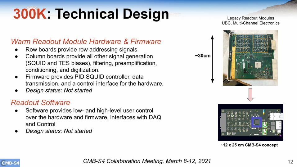
Warm Readout Module Hardware & Firmware● Row boards provide row addressing signals● Column boards provide all other signal generation
(SQUID and TES biases), filtering, preamplification, conditioning, and digitization.
● Firmware provides PID SQUID controller, data transmission, and a control interface for the hardware.
● Design status: Not started
Readout Software● Software provides low- and high-level user control
over the hardware and firmware, interfaces with DAQ and Control
● Design status: Not started
Legacy Readout ModulesUBC, Multi-Channel Electronics
~12 x 25 cm CMB-S4 concept
~30cm
CMB-S4 Collaboration Meeting, March 8-12, 2021
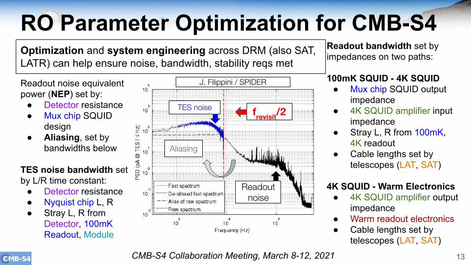
Optimization and system engineering across DRM (also SAT, LATR) can help ensure noise, bandwidth, stability reqs met
13
RO Parameter Optimization for CMB-S4
J. Filippini / SPIDER
frevisit/2
Readout noise
Aliasing
TES noise
Readout noise equivalent power (NEP) set by:
● Detector resistance● Mux chip SQUID
design● Aliasing, set by
bandwidths below
TES noise bandwidth set by L/R time constant:
● Detector resistance● Nyquist chip L, R● Stray L, R from
Detector, 100mK Readout, Module
Readout bandwidth set by impedances on two paths:
100mK SQUID - 4K SQUID ● Mux chip SQUID output
impedance● 4K SQUID amplifier input
impedance● Stray L, R from 100mK,
4K readout● Cable lengths set by
telescopes (LAT, SAT)
4K SQUID - Warm Electronics● 4K SQUID amplifier output
impedance● Warm readout electronics ● Cable lengths set by
telescopes (LAT, SAT)
CMB-S4 Collaboration Meeting, March 8-12, 2021 14
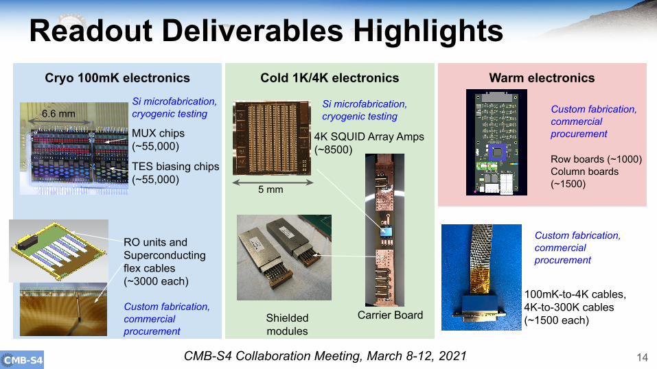
Readout Deliverables HighlightsCryo 100mK electronics Cold 1K/4K electronics Warm electronics
MUX chips(~55,000)
5 mm
TES biasing chips(~55,000)
100mK-to-4K cables, 4K-to-300K cables(~1500 each)
4K SQUID Array Amps (~8500)
Row boards (~1000) Column boards (~1500)
Si microfabrication, cryogenic testing Custom fabrication,
commercial procurement
Custom fabrication, commercial procurement
Si microfabrication, cryogenic testing6.6 mm
Carrier BoardShielded modules
RO units and Superconducting flex cables(~3000 each)
Custom fabrication, commercial procurement
CMB-S4 Collaboration Meeting, March 8-12, 2021
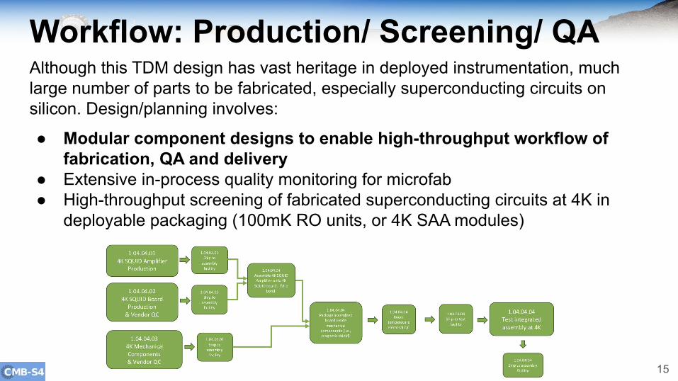
Although this TDM design has vast heritage in deployed instrumentation, much large number of parts to be fabricated, especially superconducting circuits on silicon. Design/planning involves:
● Modular component designs to enable high-throughput workflow of fabrication, QA and delivery
● Extensive in-process quality monitoring for microfab● High-throughput screening of fabricated superconducting circuits at 4K in
deployable packaging (100mK RO units, or 4K SAA modules)
15
Workflow: Production/ Screening/ QA
CMB-S4 Collaboration Meeting, March 8-12, 2021
● CMB-S4 will implement DC voltage biasing and time-division multiplexed readout of its TES bolometers
● We have an implementation concept, some mature designs and preliminary parameters to use for prototyping based on Stage-2 and Stage-3 experience
● Engineering design for preliminary baseline has commenced where possible with limited resources, although mostly outstanding.
● Incorporating design features for ease of production, screening, QA
● DRM parameter optimization and system engineering can help avoid missed requirements. Ultimately, validation of design will come from testing the performance of prototypes.
16
Summary/Conclusions
CMB-S4 Collaboration Meeting, March 8-12, 2021
Backup slides
CMB-S4 Collaboration Meeting, March 8-12, 2021 18
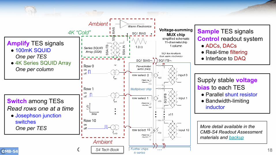
Ambient
4K “Cold”
AmbientS4 Tech Book
Supply stable voltage bias to each TES
● Parallel shunt resistor● Bandwidth-limiting
inductor
Amplify TES signals● 100mK SQUID
One per TES● 4K Series SQUID Array
One per column
Switch among TESsRead rows one at a time
● Josephson junction switchesOne per TES
Sample TES signals Control readout system
● ADCs, DACs● Real-time filtering● Interface to DAQ
More detail available in the CMB-S4 Readout Assessment materials and backup
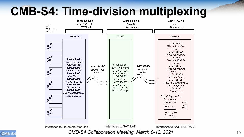
CMB-S4 Collaboration Meeting, March 8-12, 2021 19
CMB-S4: Time-division multiplexing
Interfaces to Detectors/Modules Interfaces to SAT, LAT Interfaces to SAT, LAT, DAQ
CMB-S4 Collaboration Meeting, March 8-12, 2021
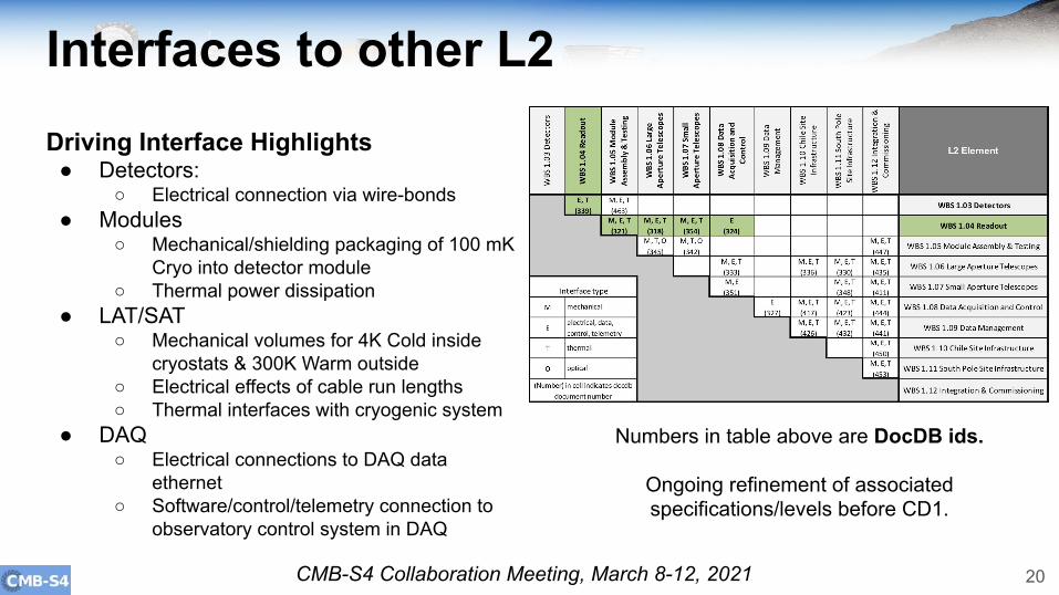
Driving Interface Highlights● Detectors:
○ Electrical connection via wire-bonds● Modules
○ Mechanical/shielding packaging of 100 mK Cryo into detector module
○ Thermal power dissipation● LAT/SAT
○ Mechanical volumes for 4K Cold inside cryostats & 300K Warm outside
○ Electrical effects of cable run lengths○ Thermal interfaces with cryogenic system
● DAQ ○ Electrical connections to DAQ data
ethernet○ Software/control/telemetry connection to
observatory control system in DAQ
20
Interfaces to other L2
Numbers in table above are DocDB ids.
Ongoing refinement of associated specifications/levels before CD1.
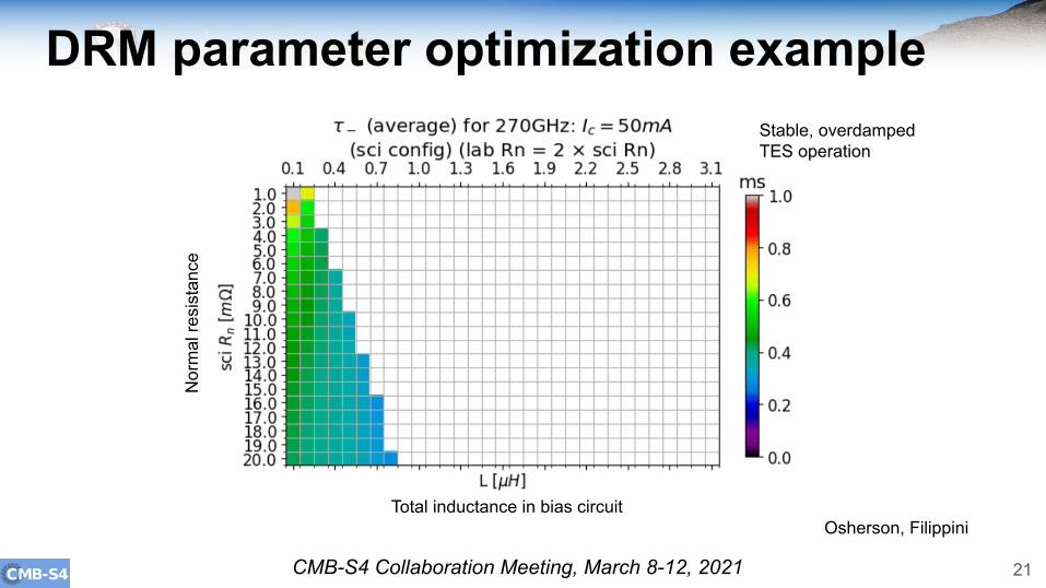
CMB-S4 Collaboration Meeting, March 8-12, 2021 21
DRM parameter optimization example
Osherson, Filippini
Nor
mal
resi
stan
ce
Total inductance in bias circuit
Stable, overdamped TES operation