Embed Size (px)
Citation preview
arX
iv:1
112.
0644
v3 [
astr
o-ph
.IM]
10 F
eb 2
012
1
Readout system with on-board demodulation forCMB polarization experiments using coherent
polarimeter arraysKoji Ishidoshiro, Makoto Nagai, Takeo Higuchi, Masaya Hasegawa,
Masashi Hazumi, Masahiro Ikeno, Osamu Tajima, Manobu Tanaka, Tomohisa Uchida
Abstract—B-modes are special patterns in cosmic microwavebackground (CMB) polarization. Degree-scale B-modes aresmoking-gun signatures of primordial gravitational waves. Thegeneric strategy of CMB polarization experiments is to employa large number of polarimeters for improving the statistics.The Q/U Imaging ExperimenT-II (QUIET-II) has been pro-posed to detectB-modes by using the world’s largest coherentpolarimeter array (2,000 channels). A unique detection tech-nique using QUIET’s polarimeters, which comprises a modu-lation/demodulation scheme, enables us to directly extract polar-ization signals. The extracted signals are free from unpolarizedcomponents and intrinsic 1/f noise. We developed a datareadout system for the QUIET-II experiment. We employed a“master” clock strategy, on-board demodulation functions, andend-to-end Ethernet connections for logical simplicity and high-density compact electronics for physical compactness. A clockmodule acts as a single master and guarantees phase matchingbetween the modulation by the polarimeters and the on-boarddemodulation by ADC modules. Each ADC module has 64ADC chips in the VME-6U single slot size. Both modules havehardware processors for Ethernet TCP/UDP. All these modulesand control computers are connected via end-to-end Ethernet.Physical compactness and logical simplicity enable us to easilyhandle a large number of polarimeters, while maintaining qualityof the B-mode experiments. The developed electronics (the clockmodules and the ADC modules) fulfill these requirements. Testswith a setup similar to that of the real experiment proved thatthe system works appropriately. The performance of all systemcomponents is validated to be suitable forB-mode measurements.
Index Terms—Readout electronics, Cosmic microwave back-ground, Demodulation, ADC
I. I NTRODUCTION
DETECTION of primordial gravitational waves couldprovide a new and unique window on the very early
universe [1]. Although various approaches for detecting them[2]–[4], the most promising approach is the measurement ofB-modes, which are odd-parity patterns in cosmic microwavebackground (CMB) polarization. BecauseB-modes are veryfaint (< 100 nK), it is important to detect a large numberof CMB photons for achieving sufficient sensitivity. The Q/UImaging ExperimenT (QUIET) is a ground-based experimentthat aims to detect theB-modes in the Atacama Desert inChile, which is 5, 080 m above sea level. At the initialphase of the QUIET experiment (QUIET-I), we observed
Manuscript received 29 November 2011: Revised 10 February 2012.Authors are with High Energy Accelerator Research Organization (KEK)
Tsukuba, Japan 305-0801 (E-mail [email protected])
CMB polarization in the 95 (43) GHz bands with 360 (72)channels of coherent polarimeter elements (polarimeter array).The obtained upper bounds for theB-modes are one of themost stringent limits to date; however they are still limited bystatistical errors [5]. An upgrade of the experiment (hereafterreferred to as QUIET-II) has been proposed to achieve bettersensitivity with a larger polarimeter array. Its primary goalis to detectB-modes atr ≈ 0.01 by using 2,000 channelscomposed of 500 elements of four-output polarimeters, wherer is the tensor-to-scalar ratio that indicates the intensityof theprimordial gravitational waves [6].
We developed a readout system for the QUIET-II exper-iments. For handling the QUIET-II polarimeter array, weemployed a master clock strategy, on-board demodulationfunctions, and end-to-end Ethernet connections for logicalsimplicity and developed high-density electronics to achievephysical compactness. The master clock strategy guaranteesphase matching between modulation and demodulation. Sincepolarization signals are modulated to suppress polarimeternoise and unpolarized components, phase matching and de-modulation functions are essential requirements for the system.The on-board demodulation has the advantage of reducing theload of data transfer. Furthermore, physical compactness isalso important to attach the system on a telescope mount toavoid picking up unexpected noise on the cables between thepolarimeter array and the readout system. In this paper, wedescribe the system design and prototype tests.
II. EXTRACTION OF THE POLARIZATION SIGNAL
A. QUIET polarimeter
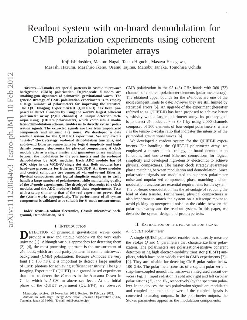
A single QUIET polarimeter enables us to directly measurethe StokesQ andU parameters that characterize liner polar-ization. The polarimeters are polarization-sensitive coherentdetectors using high electron-mobility transistor (HEMT)am-pliers, which have been widely used in CMB experiments [7]–[9]. They are suitable for detecting CMB polarization below100 GHz. The polarimeter consists of a septum polarizer andstrip-line-coupled monolithic microwave integrated circuit de-vices (Fig. 1). Input radiation is split into right and left circularpolarizations (ER andEL, respectively) by the spectrum polar-izer. In the devices, the two polarization signals are modulatedand coupled and then the power of the coupled signals isconverted to analog outputs. In the polarimeter outputs, theStokes parameters appear as the modulation components.
2
The QUIET collaboration developed a polarimeter-on-a-chip, which replaces waveguide-block components with thedevices [10]. The resulting package has a footprint size of2.5 cm× 2.5 cm (95 GHz band) and 5 cm× 5 cm (43 GHzband) in QUIET-I. This breakthrough technology enabled usto build a large polarimeter array.
B. Modulation/demodulation scheme
An HEMT amplifier is known to have a1/f noise whoseknee frequency is high approximately 1 kHz. A modula-tion/demodulation scheme is employed to extract the polar-ization signal without any contamination from the1/f noiseand unpolarized components [10]. The block diagram of themodulation is shown in Fig. 1. The inputER and EL tothe devices are amplified by HEMTs. Then, the amplifiedpolarizations are modulated by phase switches, each of whichhas two microwave paths. Path selection is controlled by p-intrinsic-n diodes. The difference among these path lengthscorresponds to a half-wavelength of the measured CMB. Thephase switch varies the phase of the CMB signal by180,which simply flips the sign of the CMB signal, and there isno sign flip for noises. Applying carrier clocks to the diodesoffers periodic phase (sign) modulation. The two amplifiedand modulated polarizations are recombined by couplers. Fourvoltage-biased square-law Schottky diodes detect the power ofthe coupled signals.
Suppose we implement the modulation only for one side,e.g., ER, then the polarimeter outputs (or diode receivingpower) can be expressed as follows (see Appendix):
D(t) = c1(t)P + c1(t)2R+ |c1(t)|2N1(t), (1)
where P is proportional tog1g2Q, −g1g2Q, g1g2U , and−g1g2U for each diode,R corresponds to the power ofthe right circular polarization, i.e., (g21E
2R). N1(t) is the
intrinsic noise of the HEMT amplifier on the side ofER,g1 and g2 are gains of the HEMT amplifier, andc1(t) isthe primary modulation term. We can setc1(t2p) = +1 andc1(t2p+1) = −1 in case of ideal modulation. Here,p is thenormalized time index with a half period ofc1(t) andD(tp)is the averaged value during thepth half period. PolarizationP can be extracted from the difference of each state, i.e.,∆D = D(t2i) − D(t2i+1). In Eq. (1), we drop the termsthat are related to the noise from another HEMT amplifier.
The modulation by the real polarimeter is not perfect, e.g.,c1(t2p) = +1 andc1(t2p+1) = −(1− ǫ1), whereǫ1 is a smallnonzero value. As a result, residual terms that are related tothe R and N1(t) appear. These residuals can be eliminatedby the secondary modulation for another side [11]. With thesecondary modulation forEL, the polarimeter output can bedescribed as follows:
D(t) = c1(t)c2(t)P + c1(t)2R+ c2(t)
2L
+|c1(t)|2N1(t) + |c2(t)|2N2(t), (2)
whereL andN2 indicate the power of the left circular po-larization (∝ g22E
2L) and the intrinsic noise on the side ofEL,
respectively. Here,c2(t) is similar toc1(t), i.e., c2(t2q) = +1and c1(t2q+1) = −(1 − ǫ2), where ǫ2 is a small nonzero
Phase switchHEMT Coupler
+
+CMB
Polarimeter
Polarimeteroutput
Carriers
Septum Monolithic microwave integrated circuit devices
E R
E L
g1×
× g2
polarizer
Fig. 1. Block diagram of the QUIET polarimeter. It consists of a septum po-larizer and strip-line-coupled monolithic microwave integrated circuit devices.The input radiation is split into right and left circular polarizations (ER andEL, respectively) by the septum polarizer. They are amplified by the HEMTs.After applying the modulation on the phase switches, they are recombined bycouplers. The couplers have four output ports. The power of each is detectedby a Schottky diode. The four diode outputs have the modulation componentsrelated to+Q, −Q, +U , or −U Stokes parameters, respectively. Three ofthe four diodes are not shown in this diagram.
value that indicates imperfection of the second modulationand q is the normalized time index with the half period ofthe second modulation. This time period is longer than that ofthe primary modulation. Only the first term in Eq. (2) has thephase information of both modulations. Therefore, the seriesof difference allows us to extract the polarization (P ) withoutany contamination. This scheme is called demodulation. Weimplement this function in the readout system.
III. SYSTEM DESIGN
A. System structure
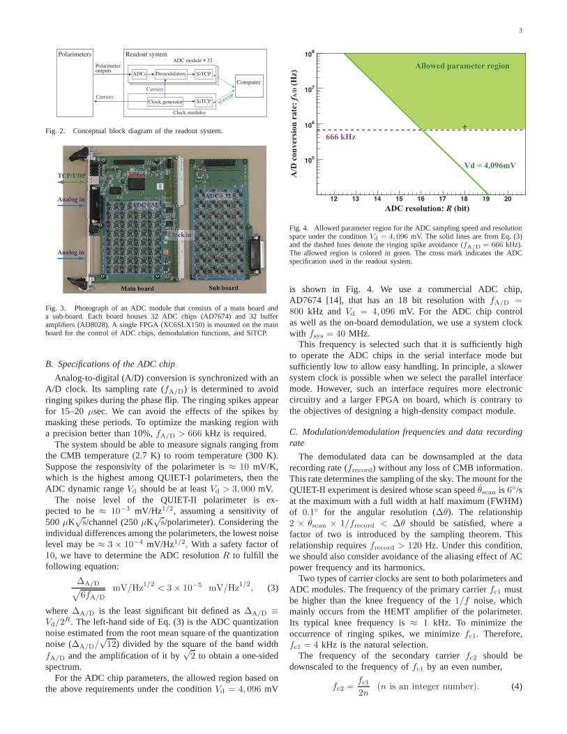
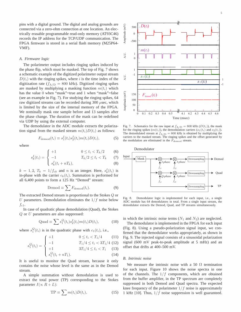
The system structure is shown in Fig. 2. The logicalsimplicity of our structure is possible because of the masterclock strategy, on-board demodulation functions, and end-to-end Ethernet connections. Clocks acts as carriers to indicatephase states for the modulation. They should be in-phasebetween the polarimeter and the readout system. To retainphase matching, we employ clock modules that work as asingle “master.” The clock modules generate well-matchedcarrier clocks and distribute them to the polarimeter arrayand analog-to-digital converter (ADC) modules. Each ADCmodule performs digitization and on-board demodulation for64 channels. Having a sub-board in addition to a mainboard, a single ADC module houses 64 ADC chips (32chips each on the main board and the sub-board) in a versamodule eurocard (VME) 6U single slot size (Fig. 3). Allcircuits for the ADC chip control and on-board demodulationare implemented in a single field programmable gate array(FPGA). Such high-density and compact modules are suitablefor attaching to the telescope mount, which is a basic schemeto suppress the noise picked up on the cable between thepolarimeters and the ADC modules.
The demodulated data in the ADC modules are transmittedto a readout computer via Ethernet transmission control pro-tocol (TCP) [12]. To control both modules from the computer,user datagram protocol (UDP) is also used. TCP and UDP inboth modules are implemented by a hardware-based processorcalled SiTCP [13]. Although to handle TCP and UDP, anadditional FPGA or CPU is usually required, we do not needthem because of the advantages of SiTCP.
3
ADCs
Computer
Clock generator
Carriers
Demodulators SiTCP
Carriers
Polarimeter outputs
Readout systemPolarimetersADC module 32+
Clock modules
SiTCP TCP/U
DP
Fig. 2. Conceptual block diagram of the readout system.
Fig. 3. Photograph of an ADC module that consists of a main board anda sub-board. Each board houses 32 ADC chips (AD7674) and 32 bufferamplifiers (AD8028). A single FPGA (XC6SLX150) is mounted onthe mainboard for the control of ADC chips, demodulation functions,and SiTCP.
B. Specifications of the ADC chip
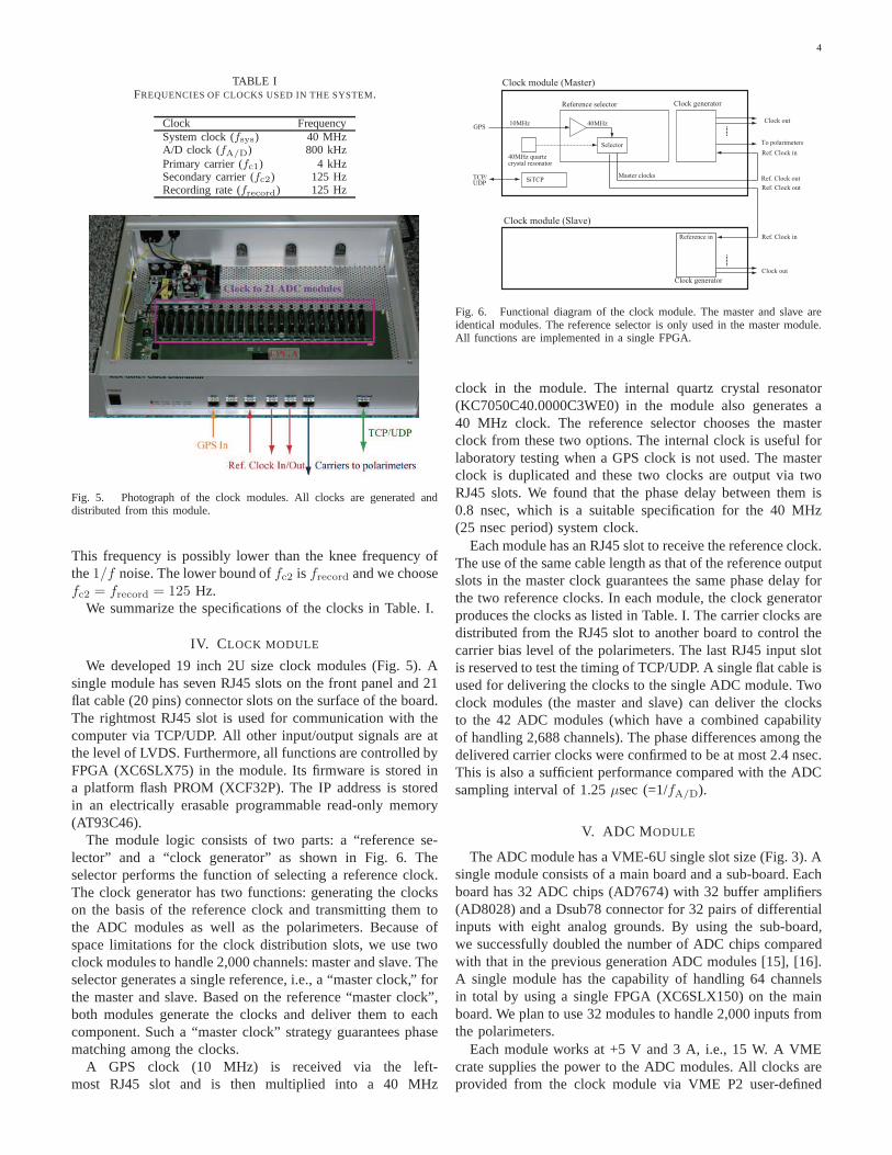
Analog-to-digital (A/D) conversion is synchronized with anA/D clock. Its sampling rate (fA/D) is determined to avoidringing spikes during the phase flip. The ringing spikes appearfor 15–20µsec. We can avoid the effects of the spikes bymasking these periods. To optimize the masking region witha precision better than 10%,fA/D > 666 kHz is required.
The system should be able to measure signals ranging fromthe CMB temperature (2.7 K) to room temperature (300 K).Suppose the responsivity of the polarimeter is≈ 10 mV/K,which is the highest among QUIET-I polarimeters, then theADC dynamic rangeVd should be at leastVd > 3, 000 mV.
The noise level of the QUIET-II polarimeter is ex-pected to be≈ 10−3 mV/Hz1/2, assuming a sensitivity of500µK
√s/channel (250µK
√s/polarimeter). Considering the
individual differences among the polarimeters, the lowestnoiselevel may be≈ 3 × 10⁻⁴ mV/Hz1/2. With a safety factor of10, we have to determine the ADC resolutionR to fulfill thefollowing equation:
∆A/D√
6fA/D
mV/Hz1/2
< 3× 10⁻⁵ mV/Hz1/2
, (3)
where∆A/D is the least significant bit defined as∆A/D ≡Vd/2
R. The left-hand side of Eq. (3) is the ADC quantizationnoise estimated from the root mean square of the quantizationnoise (∆A/D/
√12) divided by the square of the band width
fA/D and the amplification of it by√2 to obtain a one-sided
spectrum.For the ADC chip parameters, the allowed region based on
the above requirements under the conditionVd = 4, 096 mV
12 13 14 15 16 17 18 19 20
510
610
710
810
ADC resolution: R (bit)
A/D
co
nv
ersi
on
ra
te: fA
/D (
Hz)
666 kHz
Vd = 4,096mV
Allowed parameter region
+
Fig. 4. Allowed parameter region for the ADC sampling speed and resolutionspace under the conditionVd = 4, 096 mV. The solid lines are from Eq. (3)and the dashed lines denote the ringing spike avoidance (fA/D = 666 kHz).The allowed region is colored in green. The cross mark indicates the ADCspecification used in the readout system.
is shown in Fig. 4. We use a commercial ADC chip,AD7674 [14], that has an 18 bit resolution withfA/D =800 kHz and Vd = 4, 096 mV. For the ADC chip controlas well as the on-board demodulation, we use a system clockwith fsys = 40 MHz.
This frequency is selected such that it is sufficiently highto operate the ADC chips in the serial interface mode butsufficiently low to allow easy handling. In principle, a slowersystem clock is possible when we select the parallel interfacemode. However, such an interface requires more electroniccircuitry and a larger FPGA on board, which is contrary tothe objectives of designing a high-density compact module.
C. Modulation/demodulation frequencies and data recordingrate
The demodulated data can be downsampled at the datarecording rate (frecord) without any loss of CMB information.This rate determines the sampling of the sky. The mount for theQUIET-II experiment is desired whose scan speedθscan is 6/sat the maximum with a full width at half maximum (FWHM)of 0.1 for the angular resolution (∆θ). The relationship2 × θscan × 1/frecord < ∆θ should be satisfied, where afactor of two is introduced by the sampling theorem. Thisrelationship requiresfrecord > 120 Hz. Under this condition,we should also consider avoidance of the aliasing effect of ACpower frequency and its harmonics.
Two types of carrier clocks are sent to both polarimeters andADC modules. The frequency of the primary carrierfc1 mustbe higher than the knee frequency of the1/f noise, whichmainly occurs from the HEMT amplifier of the polarimeter.Its typical knee frequency is≈ 1 kHz. To minimize theoccurrence of ringing spikes, we minimizefc1. Therefore,fc1 = 4 kHz is the natural selection.
The frequency of the secondary carrierfc2 should bedownscaled to the frequency offc1 by an even number,
fc2 =fc12n
(n is an integer number). (4)
4
TABLE IFREQUENCIES OF CLOCKS USED IN THE SYSTEM.
Clock FrequencySystem clock (fsys) 40 MHzA/D clock (fA/D) 800 kHzPrimary carrier (fc1) 4 kHzSecondary carrier (fc2) 125 HzRecording rate (frecord) 125 Hz
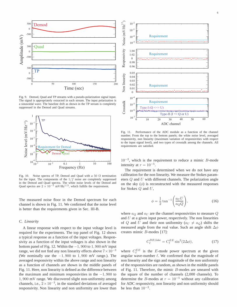
Fig. 5. Photograph of the clock modules. All clocks are generated anddistributed from this module.
This frequency is possibly lower than the knee frequency ofthe1/f noise. The lower bound offc2 is frecord and we choosefc2 = frecord = 125 Hz.
We summarize the specifications of the clocks in Table. I.
IV. CLOCK MODULE
We developed 19 inch 2U size clock modules (Fig. 5). Asingle module has seven RJ45 slots on the front panel and 21flat cable (20 pins) connector slots on the surface of the board.The rightmost RJ45 slot is used for communication with thecomputer via TCP/UDP. All other input/output signals are atthe level of LVDS. Furthermore, all functions are controlled byFPGA (XC6SLX75) in the module. Its firmware is stored ina platform flash PROM (XCF32P). The IP address is storedin an electrically erasable programmable read-only memory(AT93C46).
The module logic consists of two parts: a “reference se-lector” and a “clock generator” as shown in Fig. 6. Theselector performs the function of selecting a reference clock.The clock generator has two functions: generating the clockson the basis of the reference clock and transmitting them tothe ADC modules as well as the polarimeters. Because ofspace limitations for the clock distribution slots, we use twoclock modules to handle 2,000 channels: master and slave. Theselector generates a single reference, i.e., a “master clock,” forthe master and slave. Based on the reference “master clock”,both modules generate the clocks and deliver them to eachcomponent. Such a “master clock” strategy guarantees phasematching among the clocks.
A GPS clock (10 MHz) is received via the left-most RJ45 slot and is then multiplied into a 40 MHz
GPS40MHz
40MHz quartz crystal resonator
Clock module (Master)
10MHz
Selector
Reference selector Clock generator
Clock module (Slave)
Clock generator
Master clocks
Ref. Clock in
Reference in
Clock out
Ref. Clock in
Clock out
Ref. Clock out
Ref. Clock out
TCP/UDP
SiTCP
To polarimeters
Fig. 6. Functional diagram of the clock module. The master and slave areidentical modules. The reference selector is only used in the master module.All functions are implemented in a single FPGA.
clock in the module. The internal quartz crystal resonator(KC7050C40.0000C3WE0) in the module also generates a40 MHz clock. The reference selector chooses the masterclock from these two options. The internal clock is useful forlaboratory testing when a GPS clock is not used. The masterclock is duplicated and these two clocks are output via twoRJ45 slots. We found that the phase delay between them is0.8 nsec, which is a suitable specification for the 40 MHz(25 nsec period) system clock.
Each module has an RJ45 slot to receive the reference clock.The use of the same cable length as that of the reference outputslots in the master clock guarantees the same phase delay forthe two reference clocks. In each module, the clock generatorproduces the clocks as listed in Table. I. The carrier clocksaredistributed from the RJ45 slot to another board to control thecarrier bias level of the polarimeters. The last RJ45 input slotis reserved to test the timing of TCP/UDP. A single flat cable isused for delivering the clocks to the single ADC module. Twoclock modules (the master and slave) can deliver the clocksto the 42 ADC modules (which have a combined capabilityof handling 2,688 channels). The phase differences among thedelivered carrier clocks were confirmed to be at most 2.4 nsec.This is also a sufficient performance compared with the ADCsampling interval of 1.25µsec (=1/fA/D).
V. ADC M ODULE
The ADC module has a VME-6U single slot size (Fig. 3). Asingle module consists of a main board and a sub-board. Eachboard has 32 ADC chips (AD7674) with 32 buffer amplifiers(AD8028) and a Dsub78 connector for 32 pairs of differentialinputs with eight analog grounds. By using the sub-board,we successfully doubled the number of ADC chips comparedwith that in the previous generation ADC modules [15], [16].A single module has the capability of handling 64 channelsin total by using a single FPGA (XC6SLX150) on the mainboard. We plan to use 32 modules to handle 2,000 inputs fromthe polarimeters.
Each module works at +5 V and 3 A, i.e., 15 W. A VMEcrate supplies the power to the ADC modules. All clocks areprovided from the clock module via VME P2 user-defined
5
pins with a digital ground. The digital and analog grounds areconnected via a zero-ohm connection at one location. An elec-trically erasable programmable read-only memory (AT93C46)records the IP address for the TCP/UDP communication. TheFPGA firmware is stored in a serial flash memory (M25P64-VMF).
A. Firmware logic
The polarimeter output includes ringing spikes induced bythe phase flip, which must be masked. The top of Fig. 7 showsa schematic example of the digitized polarimeter output streamD(ti) with the ringing spikes, wherei is the time index of thedigitization rate (fA/D = 800 kHz). Digitized ringing spikesare masked by multiplying a masking functionm(ti) whichhas the value0 when “mask”=true and1 when “mask”=false(see an example in Fig. 7). For studying the ringing spikes, 64raw digitized streams can be recorded during 300µsec, whichis limited by the size of the internal memory of the FPGA.We nominally mask one sample before and 13 samples afterthe phase change. The duration of the mask can be redefinedvia UDP by using the external computer.
The demodulator in the ADC module extracts the polariza-tion signal from the masked streamm(ti)D(ti) as follows:
Fdemod(ti) ≡ sI1(ti)sI2(ti)m(ti)D(ti), (5)
where
sIk(ti) =
+1 0 ≤ ti < Tk/2 (6)
−1 Tk/2 ≤ ti < Tk (7)
sIk(ti + nTk), (8)
k = 1, 2, Tk = 1/fck and n is an integer. Here,sIk(ti) isin-phase with the carrierck(ti). Summation is performed forall 6,400 points to form a 125 Hz “Demod” stream:
Demod ≡∑
Fdemod(ti). (9)
The extracted Demod stream is proportional to the StokesQ orU parameters. Demodulation eliminates the1/f noise belowfc1.
In case of quadratic phase demodulation (Quad), the StokesQ or U parameters are also suppressed:
Quad ≡∑
sQ1 (ti)sI2(ti)m(ti)D(ti), (10)
wheresQ1 (ti) is in the quadratic phase withc1(ti), i.e.,
sQ1 (ti) =
+1 0 ≤ ti < T1/4 (11)
−1 T1/4 ≤ ti < 3T1/4 (12)
+1 3T1/4 ≤ ti < T1 (13)
sQ1 (ti + nT1). (14)
It is useful to monitor the Quad stream, because it onlycontains the noise whose level is the same as in the Demodstream.
A simple summation without demodulation is used toextract the total power (TP) corresponding to the StokesparameterI(∝ R+ L):
TP ≡∑
m(ti)D(ti), (15)
~ ~~ ~
Time (msec)
0 0.1 0.2 0.3 0.4 0.5 4.1 4.2 4.3 4.4 4.5 4.60
50
100
150
A.U
.A
mp
litu
de
(mV
)
0
1
A.U
.
1
-1
1
-1
Am
pli
tud
e (m
V)
0
500
-500
D(t )
m(t )
s (t )1
s (t )2
F (t )demod
i
i
i
i
i
Fig. 7. Schematics for the raw input atfA/D = 800 kHz (D(ti)), the maskfor the ringing spikes (m(ti)), the demodulation carriers (s1(ti) ands2(ti)).The demodulated stream atfA/D = 800 kHz is obtained by multiplying thecarriers to the masked stream. The ringing spikes and the offset generated bythe modulation are eliminated in theFdemod stream.
Downsampling
Downsampling
Input
Demodulator
Demod
Quad
I-phase I-phase
Downsampling TP
fc1 fc2
fc1 fc2
Q-phase I-phase
Mask
Fig. 8. Demodulator logic is implemented for each input, i.e., a singleADC module has 64 demodulators in total. From a single input stream, thedemodulator extracts the Demod, Quad, and TP streams simultaneously.
in which the intrinsic noise terms (N1 andN2) are neglected.The demodulator is implemented in the FPGA for each input
(Fig. 8). Using a pseudo-polarization signal input, we con-firmed that the demodulator works appropriately, as shown inFig. 9. The injected signal consists of a sinusoidal polarizationsignal (600 mV peak-to-peak amplitude at 5 mHz) and anoffset that drifts at 400–500 mV.
B. Intrinsic noise
We measure the intrinsic noise with a 50Ω terminationfor each input. Figure 10 shows the noise spectra in oneof the channels. The1/f components, which are obtainedfrom the buffer amplifier, in the TP spectrum are completelysuppressed in both Demod and Quad spectra. The expectedknee frequency of the polarimeter1/f noise is approximately1 kHz [10]. Thus,1/f noise suppression is well guaranteed.
6
0 50 100 150 200
Time (sec)
Am
pli
tude
(mV
)
0
-500
500
TP
0
-500
500 Demod
0
-500
500 Quad
Fig. 9. Demod, Quad and TP streams with a pseudo-polarization signal input.The signal is appropriately extracted in each stream. The input polarization isa sinusoidal wave. The baseline drift as shown in the TP stream is completelysuppressed in the Demod and Quad streams.
Frequency (Hz)
Nois
e le
vel
(m
V/H
z )
1/2
TP
Demod /Quad
1001010.1
1
10
10
10
10
10
-1
-2
-3
-4
-5
10-6
10-310 -2
Requirement for Demod
Fig. 10. Noise spectra of TP, Demod and Quad with a50 Ω terminationfor the input. The components of the1/f noise are completely suppressedin the Demod and Quad spectra. The white noise levels of the Demod andQuad spectra are2× 10−5 mV/Hz1/2, which fulfills the requirement.
The measured noise floor in the Demod spectrum for eachchannel is shown in Fig. 11. We confirmed that the noise levelis better than the requirements given in Sec. III-B.
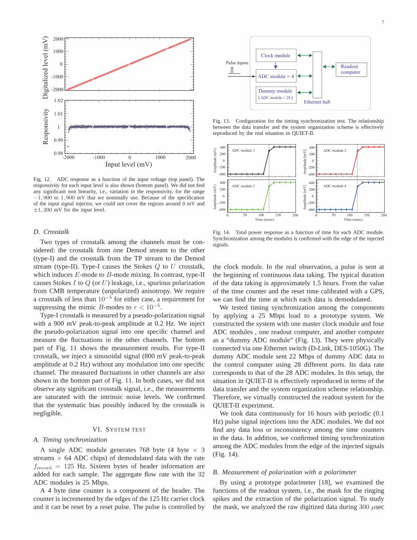
C. Linearity
A linear response with respect to the input voltage level isrequired for the experiments. The top panel of Fig. 12 showsa typical response as a function of the input voltages. Respon-sivity as a function of the input voltages is also shown in thebottom panel of Fig. 12. Within the−1, 900 to 1, 900 mV inputrange, we did not find any non linearity effects above7×10−3
(We nominally use the−1, 900 to 1, 900 mV range.). Theaveraged responsivity within the above range and non linearityas a function of channels are shown in the middle panels ofFig. 11. Here, non linearity is defined as the difference betweenthe maximum and minimum responsivities in the−1, 900 to1, 900 mV range. We discovered slight non-uniformity amongchannels, i.e.,2×10−3, in the standard deviations of averagedresponsivity. Non linearity and non uniformity are lower than
10 -2
10 -4
10 -3
10 -5
1.04
1.02
0
0.98
0.96
Nois
e (m
V/H
z )
1/2
0.05
0.04
0.03
0.02
0.01
0Non l
inea
rity
10 -4
10 -5
10 -6
10 -7
Cro
ssta
lkR
esponsi
vit
y
Requirement
Requirement
Requirement
Requirement
Type-I (Q <=> U)
Type-II (I => Q or U)
ADC channel
0 10 20 30 40 50 60
Fig. 11. Performance of the ADC module as a function of the channelnumber. From the top to the bottom panels; the white noise level, averagedresponsivity, non linearity (maximum variation of responsivities with respectto the input signal level), and two types of crosstalk among the channels. Allrequirements are satisfied.
10−2, which is the requirement to reduce a mimicB-modeintensity atr = 10−5.
The requirement is determined when we do not have anycalibration for the non linearity. We measure the Stokes param-etersQ andU with different channels. The polarization angleon the sky (φ) is reconstructed with the measured responsesfor StokesQ andU ,
φ =1
2tan−1
(
aUU
aQQ
)
, (16)
whereaQ andaU are the channel responsivities to measureQandU at a given input power, respectively. The non linearitiesof Q andU and their non uniformity (aU 6= aQ) shifts themeasured angle from the real value. Such an angle shift∆φcreates mimicB-modes [17]:
CBB,fakeℓ = CEE
ℓ sin2(2∆φ), (17)
where CEEℓ is the E-mode power spectrum at the given
angular wave-numberℓ. We confirmed that the magnitude ofnon linearity and the sign and magnitude of the non uniformityof the responsivities are random, as shown in the middle panelsof Fig. 11. Therefore, the mimicB-modes are smeared withthe square of the number of channels (2,000 channels). Todetermine theB-modes atr = 10−5 without any calibrationfor ADC responsivity, non linearity and non uniformity shouldbe less than10−2.
7
Input level (mV)-2000 -1000 0 1000 2000
Dig
ital
ized
lev
el (
mV
)
-2000
-1000
0
1000
2000
Res
ponsi
vit
y
1
1.01
1.02
0.98
0.99
Fig. 12. ADC response as a function of the input voltage (top panel). Theresponsivity for each input level is also shown (bottom panel). We did not findany significant non linearity, i.e., variation in the responsivity, for the range−1, 900 to 1, 900 mV that we nominally use. Because of the specificationof the input signal injector, we could not cover the regions around 0 mV and±1, 200 mV for the input level.
D. Crosstalk
Two types of crosstalk among the channels must be con-sidered: the crosstalk from one Demod stream to the other(type-I) and the crosstalk from the TP stream to the Demodstream (type-II). Type-I causes the StokesQ to U crosstalk,which inducesE-mode toB-mode mixing. In contrast, type-IIcauses StokesI to Q (or U ) leakage, i.e., spurious polarizationfrom CMB temperature (unpolarized) anisotropy. We requirea crosstalk of less than10−5 for either case, a requirement forsuppressing the mimicB-modes tor < 10−5.
Type-I crosstalk is measured by a pseudo-polarization signalwith a 900 mV peak-to-peak amplitude at 0.2 Hz. We injectthe pseudo-polarization signal into one specific channel andmeasure the fluctuations in the other channels. The bottompart of Fig. 11 shows the measurement results. For type-IIcrosstalk, we inject a sinusoidal signal (800 mV peak-to-peakamplitude at 0.2 Hz) without any modulation into one specificchannel. The measured fluctuations in other channels are alsoshown in the bottom part of Fig. 11. In both cases, we did notobserve any significant crosstalk signal, i.e., the measurementsare saturated with the intrinsic noise levels. We confirmedthat the systematic bias possibly induced by the crosstalk isnegligible.
VI. SYSTEM TEST
A. Timing synchronization
A single ADC module generates 768 byte (4 byte× 3streams× 64 ADC chips) of demodulated data with the ratefrecord = 125 Hz. Sixteen bytes of header information areadded for each sample. The aggregate flow rate with the32ADC modules is 25 Mbps.
A 4 byte time counter is a component of the header. Thecounter is incremented by the edges of the 125 Hz carrier clockand it can be reset by a reset pulse. The pulse is controlled by
Ethernet hub
+
4
Readout computer
Pulse inputs
ADC module +
Clock module
Dummy module
ADC module( )+ 28
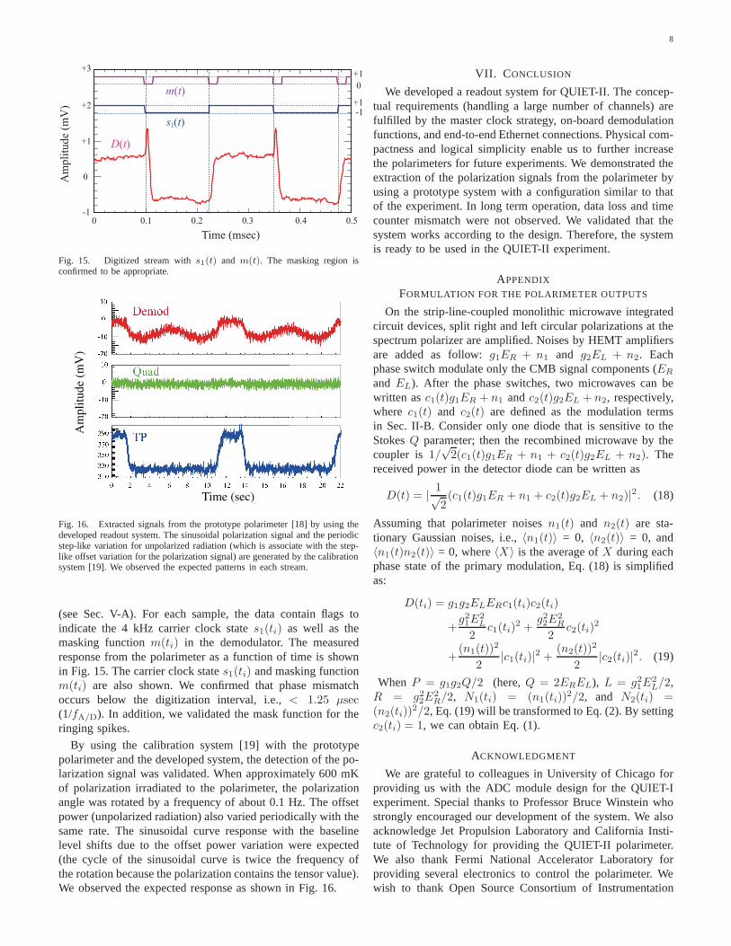
Fig. 13. Configuration for the timing synchronization test.The relationshipbetween the data transfer and the system organization scheme is effectivelyreproduced by the real situation in QUIET-II.
100500 150 200
Time (msec)
0
200
400
-200
-400Am
pli
tude
(mV
)
0
200
400
-200
-400
Am
pli
tude
(mV
)
0
200
400
-200
-400Am
pli
tude
[mV
]
0
200
400
-200
-400Am
pli
tude
[mV
]
100500 150 200
Time (msec)
ADC module 1 ADC module 2
ADC module 3 ADC module 4
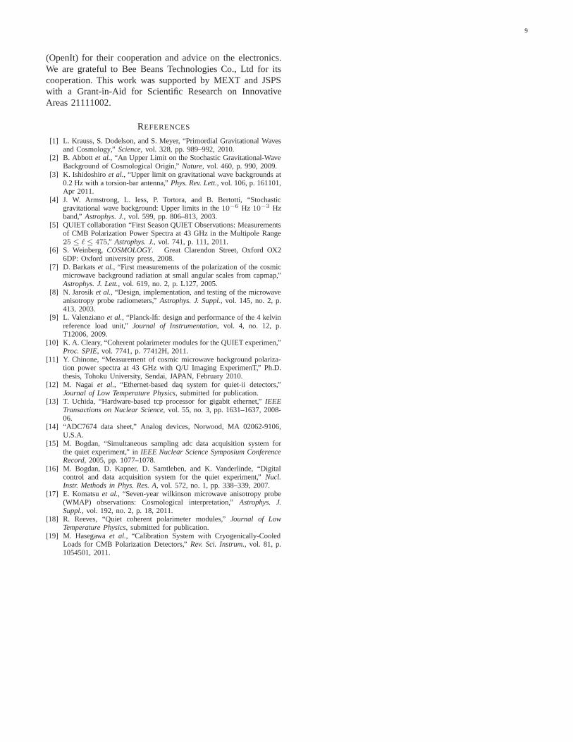
Fig. 14. Total power response as a function of time for each ADC module.Synchronization among the modules is confirmed with the edgeof the injectedsignals.
the clock module. In the real observation, a pulse is sent atthe beginning of continuous data taking. The typical durationof the data taking is approximately 1.5 hours. From the valueof the time counter and the reset time calibrated with a GPS,we can find the time at which each data is demodulated.
We tested timing synchronization among the componentsby applying a 25 Mbps load to a prototype system. Weconstructed the system with one master clock module and fourADC modules , one readout computer, and another computeras a “dummy ADC module” (Fig. 13). They were physicallyconnected via one Ethernet switch (D-Link, DES-1050G). Thedummy ADC module sent 22 Mbps of dummy ADC data tothe control computer using 28 different ports. Its data ratecorresponds to that of the 28 ADC modules. In this setup, thesituation in QUIET-II is effectively reproduced in terms ofthedata transfer and the system organization scheme relationship.Therefore, we virtually constructed the readout system fortheQUIET-II experiment.
We took data continuously for 16 hours with periodic (0.1Hz) pulse signal injections into the ADC modules. We did notfind any data loss or inconsistency among the time countersin the data. In addition, we confirmed timing synchronizationamong the ADC modules from the edge of the injected signals(Fig. 14).
B. Measurement of polarization with a polarimeter
By using a prototype polarimeter [18], we examined thefunctions of the readout system, i.e., the mask for the ringingspikes and the extraction of the polarization signal. To studythe mask, we analyzed the raw digitized data during300 µsec
8
Time (msec)
0 0.1 0.2 0.3 0.4 0.5
Am
pli
tud
e (m
V)
0
-1
+1
+2
+3
0
+1
+1-1
D(t)
m(t)
s (t)1
Fig. 15. Digitized stream withs1(t) and m(t). The masking region isconfirmed to be appropriate.
Time (sec)
Am
pli
tud
e (m
V)
Fig. 16. Extracted signals from the prototype polarimeter [18] by using thedeveloped readout system. The sinusoidal polarization signal and the periodicstep-like variation for unpolarized radiation (which is associate with the step-like offset variation for the polarization signal) are generated by the calibrationsystem [19]. We observed the expected patterns in each stream.
(see Sec. V-A). For each sample, the data contain flags toindicate the 4 kHz carrier clock states1(ti) as well as themasking functionm(ti) in the demodulator. The measuredresponse from the polarimeter as a function of time is shownin Fig. 15. The carrier clock states1(ti) and masking functionm(ti) are also shown. We confirmed that phase mismatchoccurs below the digitization interval, i.e.,< 1.25 µsec(1/fA/D). In addition, we validated the mask function for theringing spikes.
By using the calibration system [19] with the prototypepolarimeter and the developed system, the detection of the po-larization signal was validated. When approximately 600 mKof polarization irradiated to the polarimeter, the polarizationangle was rotated by a frequency of about 0.1 Hz. The offsetpower (unpolarized radiation) also varied periodically with thesame rate. The sinusoidal curve response with the baselinelevel shifts due to the offset power variation were expected(the cycle of the sinusoidal curve is twice the frequency ofthe rotation because the polarization contains the tensor value).We observed the expected response as shown in Fig. 16.
VII. C ONCLUSION
We developed a readout system for QUIET-II. The concep-tual requirements (handling a large number of channels) arefulfilled by the master clock strategy, on-board demodulationfunctions, and end-to-end Ethernet connections. Physicalcom-pactness and logical simplicity enable us to further increasethe polarimeters for future experiments. We demonstrated theextraction of the polarization signals from the polarimeter byusing a prototype system with a configuration similar to thatof the experiment. In long term operation, data loss and timecounter mismatch were not observed. We validated that thesystem works according to the design. Therefore, the systemis ready to be used in the QUIET-II experiment.
APPENDIX
FORMULATION FOR THE POLARIMETER OUTPUTS
On the strip-line-coupled monolithic microwave integratedcircuit devices, split right and left circular polarizations at thespectrum polarizer are amplified. Noises by HEMT amplifiersare added as follow:g1ER + n1 and g2EL + n2. Eachphase switch modulate only the CMB signal components (ER
and EL). After the phase switches, two microwaves can bewritten asc1(t)g1ER + n1 andc2(t)g2EL + n2, respectively,where c1(t) and c2(t) are defined as the modulation termsin Sec. II-B. Consider only one diode that is sensitive to theStokesQ parameter; then the recombined microwave by thecoupler is 1/
√2(c1(t)g1ER + n1 + c2(t)g2EL + n2). The
received power in the detector diode can be written as
D(t) = | 1√2(c1(t)g1ER + n1 + c2(t)g2EL + n2)|2. (18)
Assuming that polarimeter noisesn1(t) and n2(t) are sta-tionary Gaussian noises, i.e.,〈n1(t)〉 = 0, 〈n2(t)〉 = 0, and〈n1(t)n2(t)〉 = 0, where〈X〉 is the average ofX during eachphase state of the primary modulation, Eq. (18) is simplifiedas:
D(ti) = g1g2ELERc1(ti)c2(ti)
+g21E
2L
2c1(ti)
2 +g22E
2R
2c2(ti)
2
+(n1(t))
2
2|c1(ti)|2 +
(n2(t))2
2|c2(ti)|2. (19)
WhenP = g1g2Q/2 (here,Q = 2EREL), L = g21E2L/2,
R = g22E2R/2, N1(ti) = (n1(ti))
2/2, and N2(ti) =(n2(ti))
2/2, Eq. (19) will be transformed to Eq. (2). By settingc2(ti) = 1, we can obtain Eq. (1).
ACKNOWLEDGMENT
We are grateful to colleagues in University of Chicago forproviding us with the ADC module design for the QUIET-Iexperiment. Special thanks to Professor Bruce Winstein whostrongly encouraged our development of the system. We alsoacknowledge Jet Propulsion Laboratory and California Insti-tute of Technology for providing the QUIET-II polarimeter.We also thank Fermi National Accelerator Laboratory forproviding several electronics to control the polarimeter.Wewish to thank Open Source Consortium of Instrumentation
9
(OpenIt) for their cooperation and advice on the electronics.We are grateful to Bee Beans Technologies Co., Ltd for itscooperation. This work was supported by MEXT and JSPSwith a Grant-in-Aid for Scientific Research on InnovativeAreas 21111002.
REFERENCES
[1] L. Krauss, S. Dodelson, and S. Meyer, “Primordial Gravitational Wavesand Cosmology,”Science, vol. 328, pp. 989–992, 2010.
[2] B. Abbott et al., “An Upper Limit on the Stochastic Gravitational-WaveBackground of Cosmological Origin,”Nature, vol. 460, p. 990, 2009.
[3] K. Ishidoshiroet al., “Upper limit on gravitational wave backgrounds at0.2 Hz with a torsion-bar antenna,”Phys. Rev. Lett., vol. 106, p. 161101,Apr 2011.
[4] J. W. Armstrong, L. Iess, P. Tortora, and B. Bertotti, “Stochasticgravitational wave background: Upper limits in the10−6 Hz 10−3 Hzband,” Astrophys. J., vol. 599, pp. 806–813, 2003.
[5] QUIET collaboration “First Season QUIET Observations:Measurementsof CMB Polarization Power Spectra at 43 GHz in the Multipole Range25 ≤ ℓ ≤ 475,” Astrophys. J., vol. 741, p. 111, 2011.
[6] S. Weinberg,COSMOLOGY. Great Clarendon Street, Oxford OX26DP: Oxford university press, 2008.
[7] D. Barkatset al., “First measurements of the polarization of the cosmicmicrowave background radiation at small angular scales from capmap,”Astrophys. J. Lett., vol. 619, no. 2, p. L127, 2005.
[8] N. Jarosiket al., “Design, implementation, and testing of the microwaveanisotropy probe radiometers,”Astrophys. J. Suppl., vol. 145, no. 2, p.413, 2003.
[9] L. Valenzianoet al., “Planck-lfi: design and performance of the 4 kelvinreference load unit,”Journal of Instrumentation, vol. 4, no. 12, p.T12006, 2009.
[10] K. A. Cleary, “Coherent polarimeter modules for the QUIET experimen,”Proc. SPIE, vol. 7741, p. 77412H, 2011.
[11] Y. Chinone, “Measurement of cosmic microwave background polariza-tion power spectra at 43 GHz with Q/U Imaging ExperimenT,” Ph.D.thesis, Tohoku University, Sendai, JAPAN, February 2010.
[12] M. Nagai et al., “Ethernet-based daq system for quiet-ii detectors,”Journal of Low Temperature Physics, submitted for publication.
[13] T. Uchida, “Hardware-based tcp processor for gigabit ethernet,” IEEETransactions on Nuclear Science, vol. 55, no. 3, pp. 1631–1637, 2008-06.
[14] “ADC7674 data sheet,” Analog devices, Norwood, MA 02062-9106,U.S.A.
[15] M. Bogdan, “Simultaneous sampling adc data acquisition system forthe quiet experiment,” inIEEE Nuclear Science Symposium ConferenceRecord, 2005, pp. 1077–1078.
[16] M. Bogdan, D. Kapner, D. Samtleben, and K. Vanderlinde,“Digitalcontrol and data acquisition system for the quiet experiment,” Nucl.Instr. Methods in Phys. Res. A, vol. 572, no. 1, pp. 338–339, 2007.
[17] E. Komatsuet al., “Seven-year wilkinson microwave anisotropy probe(WMAP) observations: Cosmological interpretation,”Astrophys. J.Suppl., vol. 192, no. 2, p. 18, 2011.
[18] R. Reeves, “Quiet coherent polarimeter modules,”Journal of LowTemperature Physics, submitted for publication.
[19] M. Hasegawaet al., “Calibration System with Cryogenically-CooledLoads for CMB Polarization Detectors,”Rev. Sci. Instrum., vol. 81, p.1054501, 2011.