Embed Size (px)
Citation preview

APPLICATION NOTE
R01AN1705EJ0100 Rev. 1.00 Page 1 of 24 Jan. 6, 2014
RX63N Group, RX631 Group Read/Write Operations in 16-Bit SDRAM Using the SDRAMC
Abstract The SDRAM interface in the RX63N and RX631 Groups can be connected directly to an SDRAM up to 128 Mbytes (1024 Mbits) with a CAS latency of 1 to 3 cycles. This application note describes a method of using the RX63N Group to read from and write to a 128 Mbit SDRAM (Micron MT48LC8M16A2P-75: 2 M-word × 16 bits × 4 banks).
Products - RX63N Group 177-pin and 176-pin packages with a ROM size between 768 KB and 2 MB
- RX63N Group 145-pin and 144-pin packages with a ROM size between 768 KB and 2 MB
- RX631 Group 177-pin and 176-pin packages with a ROM size between 256 KB and 2 MB
- RX631 Group 145-pin and 144-pin packages with a ROM size between 256 KB and 2 MB
When using this application note with other Renesas MCUs, careful evaluation is recommended after making modifications to comply with the alternate MCU.
R01AN1705EJ0100 Rev. 1.00
Jan. 6, 2014

Read/Write Operations in RX63N Group, RX631 Group 16-Bit SDRAM Using the SDRAMC
R01AN1705EJ0100 Rev. 1.00 Page 2 of 24 Jan. 6, 2014
Contents
1. Specifications ..................................................................................................................................... 3
2. Operation Confirmation Conditions .................................................................................................... 4
3. Reference Application Note ................................................................................................................ 4
4. Peripheral Function ............................................................................................................................ 5 4.1 Output Operation in the SDRAMC ............................................................................................... 5
5. Hardware ............................................................................................................................................ 6 5.1 Hardware Configuration ............................................................................................................... 6 5.2 Pins Used ..................................................................................................................................... 7
6. Software ............................................................................................................................................. 8 6.1 Operation Overview ..................................................................................................................... 8
6.1.1 Configuring the SDRAM Initialization Sequence .................................................................. 8 6.1.2 Specifying the SDRAM Mode Register ............................................................................... 10 6.1.3 Specifying the Auto-Refresh Cycle ..................................................................................... 11 6.1.4 Specifying the SDRAM Read/Write Timing ........................................................................ 12
6.2 File Composition ........................................................................................................................ 14 6.3 Option-Setting Memory .............................................................................................................. 14 6.4 Constants ................................................................................................................................... 15 6.5 Functions .................................................................................................................................... 15 6.6 Function Specifications .............................................................................................................. 16 6.7 Flowcharts .................................................................................................................................. 19
6.7.1 Main Processing ................................................................................................................. 19 6.7.2 Peripheral Function Initialization ......................................................................................... 20 6.7.3 Port Initialization ................................................................................................................. 22 6.7.4 Timer Initialization for Wait Time ........................................................................................ 22 6.7.5 Wait Processing Using the CMT ......................................................................................... 23 6.7.6 SDRAM Verification Error Processing ................................................................................ 23
7. Sample Code .................................................................................................................................... 24
8. Reference Documents ...................................................................................................................... 24

Read/Write Operations in RX63N Group, RX631 Group 16-Bit SDRAM Using the SDRAMC
R01AN1705EJ0100 Rev. 1.00 Page 3 of 24 Jan. 6, 2014
1. Specifications The SDRAMC is used to read from and write to a 128 Mbit SDRAM (Micron MT48LC8M16A2P-75: 2 M-word × 16 bits × 4 banks).
After a reset, the SDRAM is initialized, and data is written in word units to the 128 Mbit SDRAM area. After data has been written to all areas, the written values are read.
When the read value matches the expected value, LED0 is turned on. If not, LED1 is turned on.
Table 1.1 lists the Peripheral Functions and Their Applications, and Table 1.2 lists the SDRAM (MT48LC8M16A2P-75) Specifications.
Table 1.1 Peripheral Functions and Their Applications
Peripheral Function Application External bus Connects to the SDRAM. I/O ports Turn on LEDs. CMT0 Timer for wait time Table 1.2 SDRAM (MT48LC8M16A2P-75) Specifications
Item Description Product Micron MT48LC8M16A2P-75 Configuration 2 M-word × 16 bits × 4 banks Size 128 Mbits Row addressing A11 to A0 Column addressing A8 to A0 Auto refresh cycle 4096 refresh cycles every 64 ms CAS latency 2 or 3 cycles Initial auto refresh 2 times AUTO REFRESH period (tRFC) 66 ns (min.) WRITE recovery time 28.33 ns (min.) PRECHARGE command period (tRP) 20 ns (min.) ACTIVE-to-PRECHARGE command period (tRAS) 44 ns (min.) ACTIVE-to-READ or WRITE delay (tRCD) 20 ns (min.)

Read/Write Operations in RX63N Group, RX631 Group 16-Bit SDRAM Using the SDRAMC
R01AN1705EJ0100 Rev. 1.00 Page 4 of 24 Jan. 6, 2014
2. Operation Confirmation Conditions The sample code accompanying this application note has been run and confirmed under the conditions below.
Table 2.1 Operation Confirmation Conditions
Item Contents MCU used R5F563NBDDFC (RX63N Group)
Operating frequencies
- Main clock: 12 MHz - PLL: 192 MHz (main clock divided by 1 and multiplied by 16) - System clock (ICLK): 96 MHz (PLL divided by 2) - Peripheral module clock B (PCLKB): 48 MHz (PLL divided by 4) - SDRAM clock (SDCLK): 48 MHz (PLL divided by 4)
Operating voltage 3.3 V Integrated development environment
Renesas Electronics Corporation High-performance Embedded Workshop Version 4.09.01
C compiler
Renesas Electronics Corporation C/C++ Compiler Package for RX Family V.1.02 Release 01
Compile options -cpu=rx600 -output=obj="$(CONFIGDIR)\$(FILELEAF).obj" -debug -nologo (The default setting is used in the integrated development environment.)
iodefine.h version Version 1.6A Endian Little endian Operating mode Single-chip mode Processor mode Supervisor mode Sample code version Version 1.00
Board used Renesas Starter Kit+ for RX63N (product part no.: R0K50563NC000BE) (SDRAM: MT48LC8M16A2P-75)
3. Reference Application Note For additional information associated with this document, refer to the following application note.
- RX63N Group, RX631 Group Initial Setting Rev. 1.10 (R01AN1245EJ0110_RX63N) The initial setting functions in the reference application note are used in the sample code in this application note. The revision number of the reference application note is the one when this application note was made. However the latest version is always recommended. Visit the Renesas Electronics Corporation website to check and download the latest version.

Read/Write Operations in RX63N Group, RX631 Group 16-Bit SDRAM Using the SDRAMC
R01AN1705EJ0100 Rev. 1.00 Page 5 of 24 Jan. 6, 2014
4. Peripheral Function This chapter provides supplementary information on the SDRAMC. Refer to the RX63N Group, RX631 Group User’s Manual: Hardware for basic information.
4.1 Output Operation in the SDRAMC With the RX63N SDRAMC, when an SDRAM command is issued, pin states associated with the SDRAM will be changed after a certain time of delay from the rising of SDCLK. The command is determined on the next rising edge of SDCLK. Refer to the Electrical Characteristics chapter in the User’s Manual: Hardware for details of the output delay time for each pin.
Figure 4.1 shows the Output on Pins Associated with the SDRAM and the Timing of Command Determination.
SDCLK
SDRAM command output
SDCS#
RAS#
CAS#
WE#
CKE#
ACT RD DSL PRA DSL DSL DSL
ACT RD DSL PRA DSL DSLSDRAM command determination
ACT : Bank active command
RD : Read command
PRA : All bank precharege command
DSL : Device deselect command
SDRAMassociated pins
The SDRAM command is output after a delay from the rising of SDCLK.
The SDRAM determines the command on the rising edge of SDCLK.
Figure 4.1 Output on Pins Associated with the SDRAM and the Timing of Command Determination

Read/Write Operations in RX63N Group, RX631 Group 16-Bit SDRAM Using the SDRAMC
R01AN1705EJ0100 Rev. 1.00 Page 6 of 24 Jan. 6, 2014
5. Hardware
5.1 Hardware Configuration Figure 5.1 shows the Connection Example.
RX63N
A14 to A13A12 to A1D15 to D0
SDCS#RAS#CAS#WE#CKE
SDCLKDQM0DQM1
SDRAM (1)
BA1 to BA0A11 to A0DQ15 to DQ0CS#RAS#CAS#WE#CKECLKDQMLDQMH
21216
Note: 1. SDRAM: MT48LC8M16A2P-75 (2 M-word × 16 bits × 4 banks)
Figure 5.1 Connection Example

Read/Write Operations in RX63N Group, RX631 Group 16-Bit SDRAM Using the SDRAMC
R01AN1705EJ0100 Rev. 1.00 Page 7 of 24 Jan. 6, 2014
5.2 Pins Used Table 5.1 lists the Pins Used and Their Functions.
Table 5.1 Pins Used and Their Functions
Pin Name I/O Function P03 Output Outputs for LED0 (verification succeeded). P05 Output Outputs for LED1 (verification error). PA7 to PA0 Output Outputs an address (A7 to A0). PB6 to PB0 Output Outputs an address (A14 to A8.) PD7 to PD0 I/O Outputs data (D7 to D0). PE7 to PE0 I/O Outputs data (D15 to D8.) P70 Output Outputs the SDCLK signal. P61 Output Outputs the SDCS# signal. P62 Output Outputs the RAS# signal. P63 Output Outputs the CAS# signal. P64 Output Outputs the WE# signal. P65 Output Outputs the CKE signal. P66 Output Outputs the DQM0 signal. P67 Output Outputs the DQM1 signal.

Read/Write Operations in RX63N Group, RX631 Group 16-Bit SDRAM Using the SDRAMC
R01AN1705EJ0100 Rev. 1.00 Page 8 of 24 Jan. 6, 2014
6. Software
6.1 Operation Overview The initialization sequence, SDRAM mode register, auto refresh cycle, and SDRAM read/write timing are specified according to the SDRAM used.
This application note introduces an example of SDRAMC configuration with the Micron SDRAM (MT48LC8M16A2P-75).
6.1.1 Configuring the SDRAM Initialization Sequence After a reset, the SDRAM must be initialized before it can be used. Configure the initialization sequence considering AUTO REFRESH period (tRFC), number of times for initial auto refresh, PRECHARGE command period (tRP), and other settings according to the datasheet for the SDRAM.
Figure 6.1 shows the Timing of SDRAM (MT48LC8M16A2P-75) Initialization and Table 6.1 lists the Example of the SDRAMC Initial Sequence Settings when Connecting to the SDRAM (MT48LC8M16A2P-75).
PRA RFA
: All bank precharge command
: Auto-refresh command
100 µs tRP tRFC(1) (2) (3) (4)
tRFC
RESET
CKE#
SDCLK
SDRAM command
(5)
RFA
PRA
RFA
Figure 6.1 Timing of SDRAM (MT48LC8M16A2P-75) Initialization
(1) After a reset, specifies pins associated with the SDRAM, sets the SYSCR0.EXBE bit to 1 (external bus is enabled) and starts outputting on the SDCLK pin. Then a high level signal is output from the CKE# pin. The CKE# pin is connected to GND through a resistor to drive the CKE# pin low after the power is turned on.
(2) Waits for 100 µs or longer after the clock is started to output. The device deselect command is output during the wait time. Then specifies the initialization timing to the SDIR register and sets the SDICR.INIRQ bit to 1, then the all bank precharge command is output.
(3) After the all bank precharge command is output, the auto-refresh command is output after the number of cycles specified by the SDIR.PRC[2:0] bits elapse. Set the value for the SDIR.PRC[2:0] bits to tRP or greater.
(4) After the auto-refresh command is output, the wait time in cycles specified by the SDIR.ARFI[2:0] bits is inserted. Set the value for SDIR.ARFI[2:0] bits to tRFC or greater.
When the number of initialization auto-refresh is set to 2 times or more by the SDIR.ARFC[3:0] bits, the auto-refresh command is output again.
(5) After the auto-refresh command is output for the number of times specified by the SDIR.ARFC[3:0] bits, the initial sequence is complete.

Read/Write Operations in RX63N Group, RX631 Group 16-Bit SDRAM Using the SDRAMC
R01AN1705EJ0100 Rev. 1.00 Page 9 of 24 Jan. 6, 2014
Table 6.1 Example of the SDRAMC Initial Sequence Settings when Connecting to the SDRAM (MT48LC8M16A2P-75)
SDRAM Timing Symbol Setting Value Setting in the SDRAMC with RX63N Wait time until the PRECHARGE command is input after SDCLK is input
— 100 μs After starting to output SDCLK, waits for 100 μs by the software, and starts the initial sequence.
PRECHARGE command period tRP 20 ns (min.) SDIR.PRC[2:0] = 000b: 3 cycles (approx. 62 ns when SDCLK is 48 MHz)
AUTO REFRESH period tRFC 66 ns (min.) SDIR.ARFI[2:0] = 001b: 4 cycles (approx. 83 ns when SDCLK is 48 MHz)
Initial auto refresh — 2 times SDIR.ARFC[3:0] = 0010b: 2 times
Read/Write Operations in RX63N Group, RX631 Group 16-Bit SDRAM Using the SDRAMC
R01AN1705EJ0100 Rev. 1.00 Page 10 of 24 Jan. 6, 2014
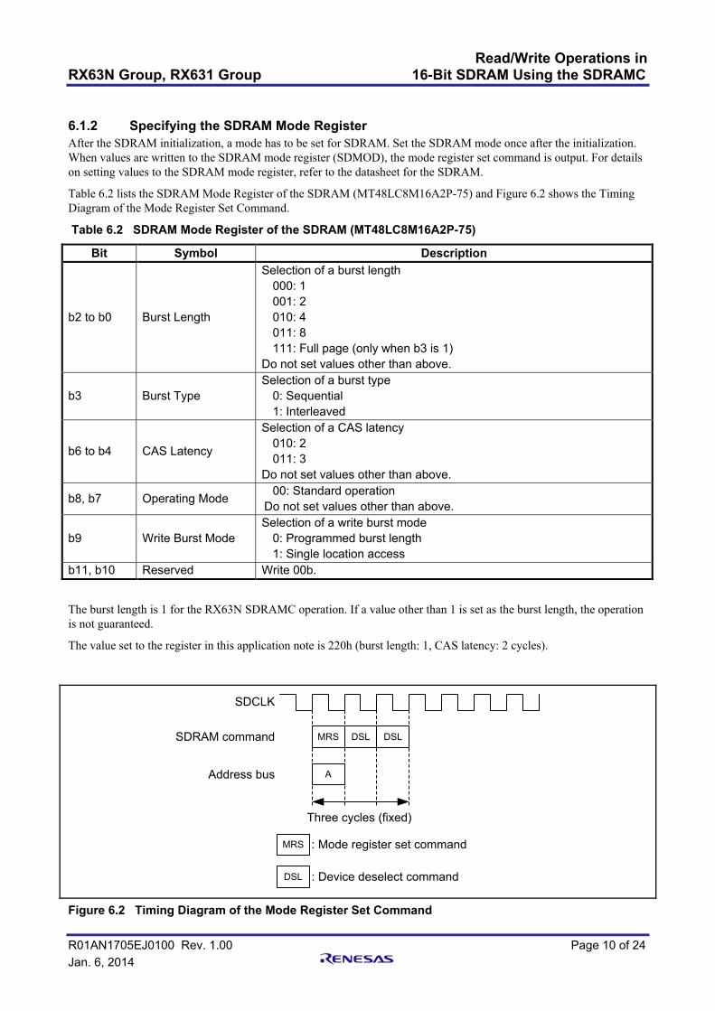
6.1.2 Specifying the SDRAM Mode Register After the SDRAM initialization, a mode has to be set for SDRAM. Set the SDRAM mode once after the initialization. When values are written to the SDRAM mode register (SDMOD), the mode register set command is output. For details on setting values to the SDRAM mode register, refer to the datasheet for the SDRAM.
Table 6.2 lists the SDRAM Mode Register of the SDRAM (MT48LC8M16A2P-75) and Figure 6.2 shows the Timing Diagram of the Mode Register Set Command.
Table 6.2 SDRAM Mode Register of the SDRAM (MT48LC8M16A2P-75)
Bit Symbol Description
b2 to b0 Burst Length
Selection of a burst length 000: 1 001: 2 010: 4 011: 8 111: Full page (only when b3 is 1)
Do not set values other than above.
b3 Burst Type Selection of a burst type
0: Sequential 1: Interleaved
b6 to b4 CAS Latency
Selection of a CAS latency 010: 2 011: 3
Do not set values other than above.
b8, b7 Operating Mode 00: Standard operation Do not set values other than above.
b9 Write Burst Mode Selection of a write burst mode
0: Programmed burst length 1: Single location access
b11, b10 Reserved Write 00b.
The burst length is 1 for the RX63N SDRAMC operation. If a value other than 1 is set as the burst length, the operation is not guaranteed.
The value set to the register in this application note is 220h (burst length: 1, CAS latency: 2 cycles).
: Mode register set command
: Device deselect command
SDCLK
SDRAM command
Address bus A
Three cycles (fixed)
MRS DSL DSL
MRS
DSL
Figure 6.2 Timing Diagram of the Mode Register Set Command

Read/Write Operations in RX63N Group, RX631 Group 16-Bit SDRAM Using the SDRAMC
R01AN1705EJ0100 Rev. 1.00 Page 11 of 24 Jan. 6, 2014
6.1.3 Specifying the Auto-Refresh Cycle To retain data in the SDRAM, a refresh must be performed for the number of rows during the refresh period (tREF). Auto-refresh must be performed considering the refresh period (tREF), number of rows, AUTO REFRESH period (tRFC), and other settings according to the datasheet for the SDRAM.
Table 6.3 lists the AUTO REFRESH Timing for the SDRAM (MT48LC8M16A2P-75) and Figure 6.3 shows the AUTO REFRESH Operating Timing.
Table 6.3 AUTO REFRESH Timing for the SDRAM (MT48LC8M16A2P-75)
SDRAM Timing Symbol Setting Value Setting in the SDRAMC with RX63N Refresh period tREF 64 ms Used for calculating AUTO REFRESH cycle Number of rows — 4096 Used for calculating AUTO REFRESH cycle
Auto refresh cycle — 15.625 μs
(tREF ÷ number of rows) SDRFCR.RFC[11:0] = 02EDh: 750 cycles (approx. 15.625 μs when SDCLK is 48 MHz)
AUTO REFRESH period tRFC 66 ns (min.) SDRFCR.REFW[3:0] = 0011b: 4 cycles
(approx. 83 ns when SDCLK is 48 MHz)
: Device deselect command
: Auto-refresh command
SDCLK
SDRAM command
tRFC tRFC
(1) (2)
Auto refresh request period
(3)
DSLRFA DSL DSL DSLRFA DSL DSL
RFA
DSL
Figure 6.3 AUTO REFRESH Operating Timing
(1) When the SDRFEN.RFEN bit is set to 1 (auto-refresh operation is enabled), the auto-refresh command is output.
(2) After the auto-refresh command is output, the device deselect command is output until the number of cycles specified by the SDRFCR.REFW[3:0] bits elapse. Set a value for the SDRFCR.REFW[3:0] bits to tRFC or greater.
(3) The auto-refresh command is output every number of cycles specified by the SDRFCR.RFC[11:0] bits. Set a value for the SDRFCR.RFC[11:0] bits to be the auto refresh cycle (tREF ÷ number of rows) or less.

Read/Write Operations in RX63N Group, RX631 Group 16-Bit SDRAM Using the SDRAMC
R01AN1705EJ0100 Rev. 1.00 Page 12 of 24 Jan. 6, 2014
6.1.4 Specifying the SDRAM Read/Write Timing The SDRAM read/write timing is specified considering the SDRAM settings of CAS latency (CL), WRITE recovery time (tWR), PRECHARGE command period (tRP), ACTIVE-to-PRECHARGE command (tRAS), and ACTIVE-to-READ or WRITE delay (tRCD).
Table 6.4 lists the Read/Write Timing when Connecting to the SDRAM (MT48LC8M16A2P-75), Figure 6.4 shows the Read timing, and Figure 6.5 shows the Write timing.
Table 6.4 Read/Write Timing when Connecting to the SDRAM (MT48LC8M16A2P-75)
SDRAM Timing Symbol Setting Value Setting in the SDRAMC with RX63N CAS latency (2) — 2 or 3 (1) DTR.CL[2:0] = 010b: 2 cycles
WRITE recovery time tWR 28.3 ns (min.) SDTR.WR = 1: 2 cycles (approx. 42 ns when SDCLK is 48 MHz)
PRECHARGE command period tRP 20 ns (min.) SDTR.RP[2:0] = 000b: 1 cycle (approx. 21 ns when SDCLK is 48 MHz)
ACTIVE-to-PRECHARGE command period (2) tRAS 44 ns (min.) SDTR.RAS[2:0] = 010b: 3 cycles
(approx. 62 ns when SDCLK is 48 MHz) ACTIVE-to-READ or WRITE delay (2) tRCD 20 ns (min.) SDTR.RCD[1:0] = 00b: 1 cycle
(approx. 21 ns when SDCLK is 48 MHz) Notes:
1. Select ‘2’ in the SDRAM mode setting. 2. Set a value for the ACTIVE-to-PRECHARGE command period to less than or equal to ACTIVE-to-
READ or WRITE delay (SDTR.RCD[1:0] + DTR.CL[2:0]).
: Bank active command
: Device deselect command
SDCLK
SDRAM command
Data bus
ACT
tRCD
RD DSL PRA
data
CL
tRAS
Single read
tRP
: Read command
: All bank precharge command
ACT
RD
DSL
PRA
Figure 6.4 Read Timing when the SDRAMC with Setting in Table 6.4 is Used

Read/Write Operations in RX63N Group, RX631 Group 16-Bit SDRAM Using the SDRAMC
R01AN1705EJ0100 Rev. 1.00 Page 13 of 24 Jan. 6, 2014
: Bank active command
: Device deselect command
SDCLK
SDRAM command
Data bus
ACT
tRCD
WRI DSL PRA
data
tWR
tRAS
Single write
tRP
: Write command
: All bank precharge command
ACT
WRI
PRA
DSL
Figure 6.5 Write Timing when the SDRAMC with Setting in Table 6.4 is Used

Read/Write Operations in RX63N Group, RX631 Group 16-Bit SDRAM Using the SDRAMC
R01AN1705EJ0100 Rev. 1.00 Page 14 of 24 Jan. 6, 2014
6.2 File Composition Table 6.5 lists the Files Used in the Sample Code. Files generated by the integrated development environment are not included in this table.
Table 6.5 Files Used in the Sample Code
File Name Outline Remarks main.c Main processing
r_init_stop_module.c Stop processing for active peripheral functions after a reset
r_init_stop_module.h Header file for r_init_stop_module.c r_init_non_existent_port.c Nonexistent port initialization r_init_non_existent_port.h Header file for r_init_non_existent_port.c r_init_clock.c Clock initialization r_init_clock.h Header file for r_init_clock.c r_cmt_wait.c Wait processing using the CMT r_cmt_wait.h Header file for r_cmt_wait.c
6.3 Option-Setting Memory Table 6.6 lists the Option-Setting Memory Configured in the Sample Code. When necessary, set a value suited to the user system.
Table 6.6 Option-Setting Memory Configured in the Sample Code
Symbol Address Setting Value Contents
OFS0 FFFF FF8Fh to FFFF FF8Ch FFFF FFFFh The IWDT is stopped after a reset. The WDT is stopped after a reset.
OFS1 FFFF FF8Bh to FFFF FF88h FFFF FFFFh The voltage monitor 0 reset is disabled after a reset. HOCO oscillation is disabled after a reset.
MDES FFFF FF83h to FFFF FF80h FFFF FFFFh Little endian

Read/Write Operations in RX63N Group, RX631 Group 16-Bit SDRAM Using the SDRAMC
R01AN1705EJ0100 Rev. 1.00 Page 15 of 24 Jan. 6, 2014
6.4 Constants Table 6.7 lists the Constants Used in the Sample Code.
Table 6.7 Constants Used in the Sample Code
Constant Name Setting Value Contents LED0_REG_PODR PORT0.PODR.BIT.B3 LED0 output data store bit LED0_REG_PDR PORT0.PDR.BIT.B3 LED0 I/O select bit LED0_REG_PMR PORT0.PMR.BIT.B3 LED0 pin mode control bit LED1_REG_PODR PORT1.PODR.BIT.B5 LED1 output data store bit LED1_REG_PDR PORT1.PDR.BIT.B5 LED1 I/O select bit LED1_REG_PMR PORT1.PMR.BIT.B5 LED1 pin mode control bit LED_ON 0 LED output data: Turned on LED_OFF 1 LED output data: Turned off SDRAM_TOP (void*)(0x08000000) Start address of the SDRAM area SDRAM_END (void*)(0x09000000) End address of the SDRAM area R_WT_CMT_CLOCK 48000000L CMT count source frequency (PCLK) R_WT_CMT_DIVIDE 32L Division ratio of the CMT count source R_WT_BASE_US 1000000L Calculated value for the wait time for 1 μs R_WT_BASE_MS 1000L Calculated value for the wait time for 1 ms
6.5 Functions Table 6.8 lists the Functions.
Table 6.8 Functions
Function Name Outline main Main processing port_init Port initialization R_INIT_StopModule Stop processing for active peripheral functions after a reset R_INIT_NonExistentPort Nonexistent port initialization R_INIT_Clock Clock initialization R_INIT_CMT_Wait Timer initialization for wait time R_CMT_Wait Wait processing using the CMT R_WAIT_US Wait processing using the CMT (unit: μs) (1) R_WAIT_MS Wait processing using the CMT (unit: ms) (1) peripheral_init Peripheral function initialization sdram_verify_err SDRAM verification error processing Note:
1. This function is a function-like macro.

Read/Write Operations in RX63N Group, RX631 Group 16-Bit SDRAM Using the SDRAMC
R01AN1705EJ0100 Rev. 1.00 Page 16 of 24 Jan. 6, 2014
6.6 Function Specifications The following tables list the sample code function specifications.
main Outline Main processing Header None Declaration void main(void)
Description After initialization, initializes the SDRAM and performs read/write operation in the SDRAM.
Arguments None Return Value None port_init Outline Port initialization Header None Declaration static void port_init(void) Description Initializes the ports. Arguments None Return Value None R_INIT_StopModule Outline Stop processing for active peripheral functions after a reset Header r_init_stop_module.h Declaration void R_INIT_StopModule(void) Description Configures the setting to enter the module-stop state. Arguments None Return Value None Remarks Transition to the module-stop state is not performed in the sample code. Refer to the
RX63N Group, RX631 Group Initial Setting Rev. 1.10 application note for details on this function.
R_INIT_NonExistentPort Outline Nonexistent port initialization Header r_init_non_existent_port.h Declaration void R_INIT_NonExistentPort(void) Description Initializes port direction registers for ports that do not exist in products with less than
176 pins. Arguments None Return Value None Remarks The number of pins in the sample code is set for the 176-pin package
(PIN_SIZE=176). After this function is called, when writing in byte units to the PDR registers or PODR registers which have nonexistent ports, set the corresponding bits for nonexistent ports as follows: set the I/O select bits in the PDR registers to 1 and set the output data store bits in the PODR registers to 0. Refer to the RX63N Group, RX631 Group Initial Setting Rev. 1.10 application note for details on this function.

Read/Write Operations in RX63N Group, RX631 Group 16-Bit SDRAM Using the SDRAMC
R01AN1705EJ0100 Rev. 1.00 Page 17 of 24 Jan. 6, 2014
R_INIT_Clock Outline Clock initialization Header r_init_clock.h Declaration void R_INIT_Clock(void) Description Initializes the clock. Arguments None Return Value None Remarks The sample code selects processing which uses PLL as the system clock without
using the sub-clock. Refer to the RX63N Group, RX631 Group Initial Setting Rev. 1.10 application note for details on this function.
peripheral_init Outline Peripheral function initialization Header None Declaration static void peripheral_init(void) Description Initializes peripheral functions used. Arguments None Return Value None
sdram_verify_err Outline SDRAM verification error processing Header None Declaration static void sdram_verify_err(void)
Description When the SDRAM verification error occurs, turns on LED1 and executes loop processing.
Arguments None Return Value None R_INIT_CMT_Wait Outline Timer initialization for wait time Header r_cmt_wait.h Declaration void R_INIT_CMT_Wait (void) Description Initializes the timer (CMT0) for wait time. Arguments None Return Value None R_CMT_Wait Outline Wait processing using the CMT Header r_cmt_wait.h Declaration void R_CMT_Wait (uint16_t cnt) Description Waits for the time specified by the argument. Arguments uint16_t cnt: Wait time Return Value None Remarks This function is used in the R_TWAIT_US(t_us) or R_TWAIT_MS(t_ms) function.

Read/Write Operations in RX63N Group, RX631 Group 16-Bit SDRAM Using the SDRAMC
R01AN1705EJ0100 Rev. 1.00 Page 18 of 24 Jan. 6, 2014
R_WAIT_US Outline Wait processing using the CMT (unit: μs) Header r_cmt_wait.h Declaration R_WAIT_US(t_us) Description Waits for the time (μs) specified by the argument. Arguments u_int16 t_us: Wait time (μs) Return Value None
Remarks This function is a function-like macro. #define R_WAIT_US(t_us) R_ CMT_Wait(t_us * (R_WT_CMT_CLOCK / R_WT_BASE_US) / R_WT_CMT_DIVIDE)
R_WAIT_MS Outline Wait processing using the CMT (unit: ms) Header r_cmt_wait.h Declaration R_WAIT_MS(t_ms) Description Waits for the time (ms) specified by the argument. Arguments u_int16 t_ms: Wait time (ms) Return Value None
Remarks This function is a function-like macro. #define R_WAIT_MS(t_ms) R_CMT_Wait(t_ms * (R_WT_CMT_CLOCK / R_WT_BASE_MS) / R_WT_CMT_DIVIDE)

Read/Write Operations in RX63N Group, RX631 Group 16-Bit SDRAM Using the SDRAMC
R01AN1705EJ0100 Rev. 1.00 Page 19 of 24 Jan. 6, 2014
6.7 Flowcharts 6.7.1 Main Processing Figure 6.6 shows the Main Processing.
main
Initialize data in the SDRAM Writes 0000h to the whole SDRAM area.
I flag ← 0Disable maskable interrupts
Port initializationport_init()
Stop processing for active peripheral functions after a reset
R_INIT_StopModule()
Nonexistent port initializationR_INIT_NonExistentPort()
Clock initializationR_INIT_Clock()
Timer initialization for wait timeR_INIT_CMT_Wait()
Peripheral function initializationperipheral_init()
Initialize data to be written (0000h)
Target address for write operation < End address
of the SDRAM?
Yes
No
Target address for write operation = Start address of the SDRAM
Write data to the target address for write operation in the SDRAM
Increment the target address for write operation and
update the data to be written
Initialize the data to be verified (0000h)
Yes
No
Address for verification = Start address of the SDRAM
Increment the address for verification and update the data to be verified
Data in the address for verification =
Data to be verified?
Address for verification < Last address of
the SDRAM?
YesError processing
sdram_verify_err()
Turn on LED0
No
PORT0.PODR register B3 bit ← 0
Figure 6.6 Main Processing
Read/Write Operations in RX63N Group, RX631 Group 16-Bit SDRAM Using the SDRAMC
R01AN1705EJ0100 Rev. 1.00 Page 20 of 24 Jan. 6, 2014
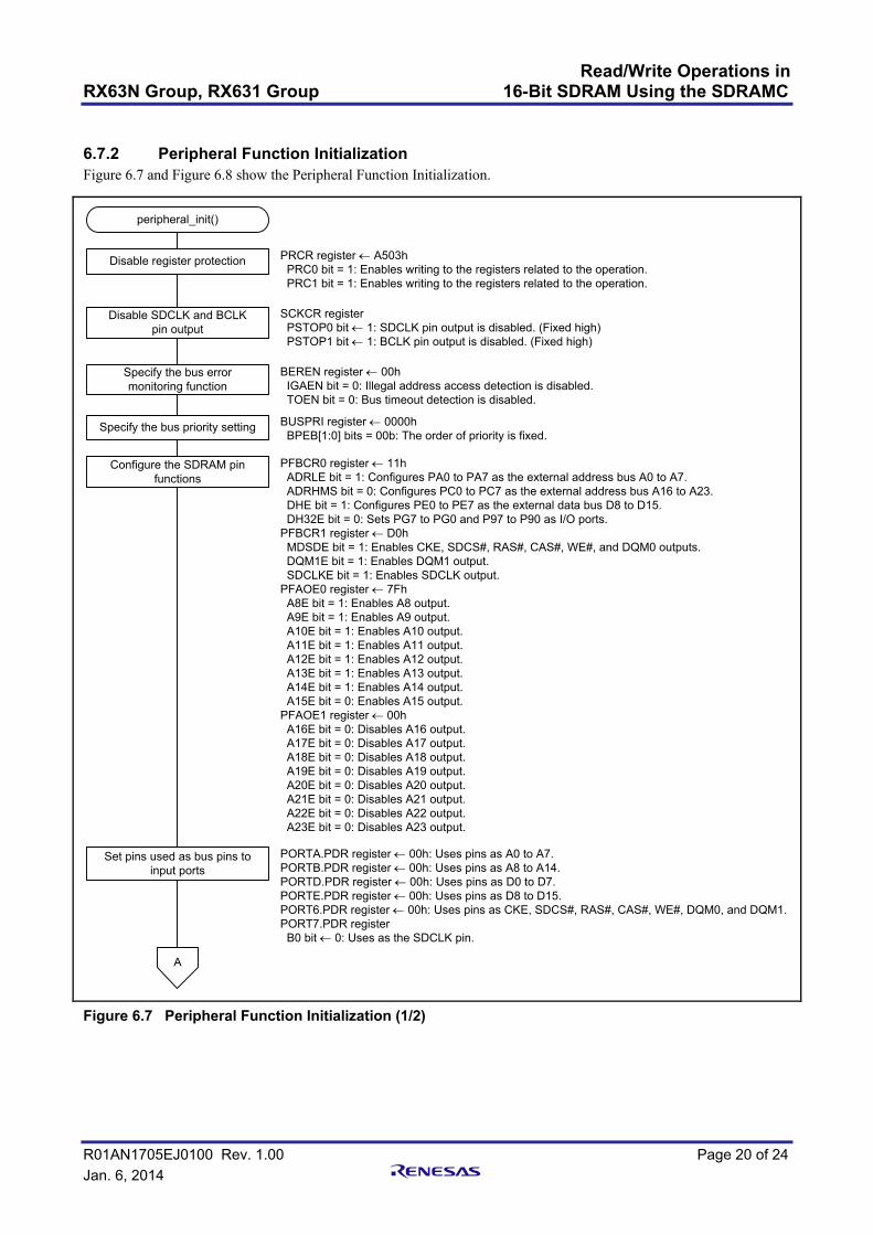
6.7.2 Peripheral Function Initialization Figure 6.7 and Figure 6.8 show the Peripheral Function Initialization.
peripheral_init()
Disable register protection
Disable SDCLK and BCLK pin output
Specify the bus error monitoring function
Specify the bus priority setting
Configure the SDRAM pin functions
Set pins used as bus pins to input ports
PRCR register ← A503h PRC0 bit = 1: Enables writing to the registers related to the operation. PRC1 bit = 1: Enables writing to the registers related to the operation.
SCKCR register PSTOP0 bit ← 1: SDCLK pin output is disabled. (Fixed high) PSTOP1 bit ← 1: BCLK pin output is disabled. (Fixed high)
BEREN register ← 00h IGAEN bit = 0: Illegal address access detection is disabled. TOEN bit = 0: Bus timeout detection is disabled.
BUSPRI register ← 0000h BPEB[1:0] bits = 00b: The order of priority is fixed.
A
PFBCR0 register ← 11h ADRLE bit = 1: Configures PA0 to PA7 as the external address bus A0 to A7. ADRHMS bit = 0: Configures PC0 to PC7 as the external address bus A16 to A23. DHE bit = 1: Configures PE0 to PE7 as the external data bus D8 to D15. DH32E bit = 0: Sets PG7 to PG0 and P97 to P90 as I/O ports. PFBCR1 register ← D0h MDSDE bit = 1: Enables CKE, SDCS#, RAS#, CAS#, WE#, and DQM0 outputs. DQM1E bit = 1: Enables DQM1 output. SDCLKE bit = 1: Enables SDCLK output. PFAOE0 register ← 7Fh A8E bit = 1: Enables A8 output. A9E bit = 1: Enables A9 output. A10E bit = 1: Enables A10 output. A11E bit = 1: Enables A11 output. A12E bit = 1: Enables A12 output. A13E bit = 1: Enables A13 output. A14E bit = 1: Enables A14 output. A15E bit = 0: Enables A15 output.PFAOE1 register ← 00h A16E bit = 0: Disables A16 output. A17E bit = 0: Disables A17 output. A18E bit = 0: Disables A18 output. A19E bit = 0: Disables A19 output. A20E bit = 0: Disables A20 output. A21E bit = 0: Disables A21 output. A22E bit = 0: Disables A22 output. A23E bit = 0: Disables A23 output.
PORTA.PDR register ← 00h: Uses pins as A0 to A7.PORTB.PDR register ← 00h: Uses pins as A8 to A14.PORTD.PDR register ← 00h: Uses pins as D0 to D7.PORTE.PDR register ← 00h: Uses pins as D8 to D15. PORT6.PDR register ← 00h: Uses pins as CKE, SDCS#, RAS#, CAS#, WE#, DQM0, and DQM1.PORT7.PDR register B0 bit ← 0: Uses as the SDCLK pin.
Figure 6.7 Peripheral Function Initialization (1/2)

Read/Write Operations in RX63N Group, RX631 Group 16-Bit SDRAM Using the SDRAMC
R01AN1705EJ0100 Rev. 1.00 Page 21 of 24 Jan. 6, 2014
Enable the external bus
Configure the initial sequence
Select the SDRAM bus width
Enable SDCLK pin output
SYSCR0 register ← 5A03h ROME bit = 1: The on-chip ROM is enabled. EXBE bit = 1: The external bus is enabled.
SDIR register ← 0021h ARFI[3:0] bits = 0001b: Initial auto-refresh interval: 4 cycles ARFC[3:0] bits = 0010b: Initial auto-refresh count: 2 times PRC[2:0] bits = 000b: Initialization precharge cycle count: 3 cycles
SDCCR register ← 00h EXENB bit = 0: Disable the SDRAM operation BSIZE[1:0] bits = 00b: A 16-bit bus space is selected.
A
SCKCR register PSTOP0 bit ← 0: SDCLK pin output is enabled.
Waits for 100 µs or longer after SDCLK is output.Wait for 100 µs after the SDCLK output
R_CMT_WAIT_US()
Start the initial sequence SDICR register ← 01h INIRQ bit = 1: Initialization sequence starts.
Confirm the status register Confirms values of bits in the SDSR register are all 0.
Select SDRAM mode SDMOD register ← 0220h MR[14:0] bits = 0220h: Setting value for the mode register set command
Select the SDRAM timing SDTR register ← 0002 0102h CL[2:0] bits = 010b: Column latency: 2 cycles WR bit = 1: Write recovery interval: 2 cycles RP[2:0] bits = 000b: Row precharge interval: 1 cycle RCD[1:0] bits = 00b: Row column latency: 1 cycle RAS[2:0] bits = 010b: Row active interval: 3 cycles
Specify the address multiplex selection
SDADR register ← 01h MXC[1:0] bits = 01b: 9-bit shift
Specify the endian setting SDCMOD register ← 00h EMODE bit = 0: Same endian as the one for the operating mode
Specify access mode SDAMOD register ← 00h BE bit = 0: Continuous access is disabled.
Specify the auto-refresh timing SDRFCR register ← 32EDh RFC[11:0] bits = 2EDh: Auto-refresh request interval setting: 750 cycles REFW[3:0] bits = 0011b: Auto-refresh cycle: 4 cycles
Enable auto-refresh operation SDRFEN register ← 01h RFEN bit = 1: Auto-refresh operation is enabled.
Enable operation in the SDRAM address space.
SDCCR register EXENB bit ← 1: Operation is enabled in the SDRAM address space.
return
Enable register protection PRCR register ← A500h PRC0 bit = 0: Disables writing to the registers related to the operation. PRC1 bit = 0: Disables writing to the registers related to the operation.
Figure 6.8 Peripheral Function Initialization (2/2)

Read/Write Operations in RX63N Group, RX631 Group 16-Bit SDRAM Using the SDRAMC
R01AN1705EJ0100 Rev. 1.00 Page 22 of 24 Jan. 6, 2014
6.7.3 Port Initialization Figure 6.9 shows the Port Initialization.
port_init
return
Specify output data for ports PORT0.PODR register B3 bit ← 1: LED0: Turned off B5 bit ← 1: LED1: Turned off
Specify the port direction
Specify mode for ports
PORT0.PDR register B3 bit ← 1: LED0: Output B5 bit ← 1: LED1: Output
PORT0.PMR register B3 bit ← 0: LED0: Uses as a general I/O pin. B5 bit ← 0: LED1: Uses as a general I/O pin.
Figure 6.9 Port Initialization
6.7.4 Timer Initialization for Wait Time Figure 6.10 shows the Timer Initialization for Wait Time.
R_INIT_CMT_Wait()
return
Store the PRCR register value
Disable register protection PRCR register ← A502h PRC1 = 1: Enables writing to the registers related to the operation.
Cancel the module-stop state MSTPCRA register MSTPA15 bit ← 0: The module-stop state is canceled for CMT0 and CMT1.
Stop the CMT0 count
Specify the CMT0 count source and enable the compare match
interrupt
CMSTR0 register STR0 bit ← 0: CMT0.CMCNT count is stopped.
CMCR register ← 00C1h CKS[1:0] bits = 01b: PCLK/32 CMIE bit = 1: Compare match interrupt (CMI0) enabled
Restore the PRCR register value
Clear the CMT0 count CMCNT register ← 0000h
Clear the CMT0 interrupt request IR028 register IR flag ← 0: No CMT0.CMI0 interrupt request is generated.
Figure 6.10 Timer Initialization for Wait Time

Read/Write Operations in RX63N Group, RX631 Group 16-Bit SDRAM Using the SDRAMC
R01AN1705EJ0100 Rev. 1.00 Page 23 of 24 Jan. 6, 2014
6.7.5 Wait Processing Using the CMT Figure 6.11 shows the Wait Processing Using the CMT.
R_CMT_Wait()
return
Stop the CMT0 count CMSTR0 register STR0 bit ← 0: CMT0.CMCNT count is stopped.
Clear the CMT0 count CMCNT register ← 0000h
Decrement the wait time cnt ← cnt - 1
Is the wait time other than 0?
Yes
No
Set the wait time for CMT0
Clear the CMT0 interrupt request
CMCOR register ← cnt
IR028 register IR flag ← 0: No CMT0.CMI0 interrupt request is generated.
Start the CMT0 count CMSTR0 register STR0 bit ← 1: CMT0.CMCNT count is started.
Stop the CMT0 count CMSTR0 register STR0 bit ← 0: CMT0.CMCNT count is stopped.
Argument: cnt: Wait time
Wait for CMI0 interrupt request generation
Read the IR028 register IR bit: 0: No CMI0 interrupt request is generated. 1: CMI0 interrupt request is generated.
Clear the CMT0 interrupt request IR028 register IR flag ← 0: No CMT0.CMI0 interrupt request is generated.
Figure 6.11 Wait Processing Using the CMT
6.7.6 SDRAM Verification Error Processing Figure 6.12 shows the SDRAM Verification Error Processing.
sdram_verify_err()
Turn on LED1 PORT0.PODR register B5 bit ← 0
Figure 6.12 SDRAM Verification Error Processing

Read/Write Operations in RX63N Group, RX631 Group 16-Bit SDRAM Using the SDRAMC
R01AN1705EJ0100 Rev. 1.00 Page 24 of 24 Jan. 6, 2014
7. Sample Code Sample code can be downloaded from the Renesas Electronics website.
8. Reference Documents User’s Manual: Hardware
RX63N Group, RX631 Group User's Manual: Hardware Rev.1.70 (R01UH0041EJ) The latest version can be downloaded from the Renesas Electronics website.
Technical Update/Technical News
The latest information can be downloaded from the Renesas Electronics website. User’s Manual: Development Tools
RX Family C/C++ Compiler Package V.1.01 User’s Manual Rev.1.00 (R20UT0570EJ) The latest version can be downloaded from the Renesas Electronics website.
Website and Support Renesas Electronics website
http://www.renesas.com Inquiries
http://www.renesas.com/contact/

A-1
REVISION HISTORY RX63N Group, RX631 Group Application Note Read/Write Operations in 16-Bit SDRAM Using the SDRAMC
Rev. Date Description
Page Summary 1.00 Jan. 6, 2014 — First edition issued
All trademarks and registered trademarks are the property of their respective owners.

General Precautions in the Handling of MPU/MCU Products The following usage notes are applicable to all MPU/MCU products from Renesas. For detailed usage notes on the products covered by this document, refer to the relevant sections of the document as well as any technical updates that have been issued for the products.
1. Handling of Unused Pins Handle unused pins in accordance with the directions given under Handling of Unused Pins in the manual. The input pins of CMOS products are generally in the high-impedance state. In operation with an
unused pin in the open-circuit state, extra electromagnetic noise is induced in the vicinity of LSI, an associated shoot-through current flows internally, and malfunctions occur due to the false recognition of the pin state as an input signal become possible. Unused pins should be handled as described under Handling of Unused Pins in the manual.
2. Processing at Power-on The state of the product is undefined at the moment when power is supplied. The states of internal circuits in the LSI are indeterminate and the states of register settings and
pins are undefined at the moment when power is supplied. In a finished product where the reset signal is applied to the external reset pin, the states of pins are not guaranteed from the moment when power is supplied until the reset process is completed. In a similar way, the states of pins in a product that is reset by an on-chip power-on reset function are not guaranteed from the moment when power is supplied until the power reaches the level at which resetting has been specified.
3. Prohibition of Access to Reserved Addresses Access to reserved addresses is prohibited. The reserved addresses are provided for the possible future expansion of functions. Do not access
these addresses; the correct operation of LSI is not guaranteed if they are accessed. 4. Clock Signals
After applying a reset, only release the reset line after the operating clock signal has become stable. When switching the clock signal during program execution, wait until the target clock signal has stabilized. When the clock signal is generated with an external resonator (or from an external oscillator)
during a reset, ensure that the reset line is only released after full stabilization of the clock signal. Moreover, when switching to a clock signal produced with an external resonator (or by an external oscillator) while program execution is in progress, wait until the target clock signal is stable.
5. Differences between Products Before changing from one product to another, i.e. to a product with a different part number, confirm that the change will not lead to problems. The characteristics of an MPU or MCU in the same group but having a different part number may
differ in terms of the internal memory capacity, layout pattern, and other factors, which can affect the ranges of electrical characteristics, such as characteristic values, operating margins, immunity to noise, and amount of radiated noise. When changing to a product with a different part number, implement a system-evaluation test for the given product.

Notice1. Descriptions of circuits, software and other related information in this document are provided only to illustrate the operation of semiconductor products and application examples. You are fully responsible for
the incorporation of these circuits, software, and information in the design of your equipment. Renesas Electronics assumes no responsibility for any losses incurred by you or third parties arising from the
use of these circuits, software, or information.
2. Renesas Electronics has used reasonable care in preparing the information included in this document, but Renesas Electronics does not warrant that such information is error free. Renesas Electronics
assumes no liability whatsoever for any damages incurred by you resulting from errors in or omissions from the information included herein.
3. Renesas Electronics does not assume any liability for infringement of patents, copyrights, or other intellectual property rights of third parties by or arising from the use of Renesas Electronics products or
technical information described in this document. No license, express, implied or otherwise, is granted hereby under any patents, copyrights or other intellectual property rights of Renesas Electronics or
others.
4. You should not alter, modify, copy, or otherwise misappropriate any Renesas Electronics product, whether in whole or in part. Renesas Electronics assumes no responsibility for any losses incurred by you or
third parties arising from such alteration, modification, copy or otherwise misappropriation of Renesas Electronics product.
5. Renesas Electronics products are classified according to the following two quality grades: "Standard" and "High Quality". The recommended applications for each Renesas Electronics product depends on
the product's quality grade, as indicated below.
"Standard": Computers; office equipment; communications equipment; test and measurement equipment; audio and visual equipment; home electronic appliances; machine tools; personal electronic
equipment; and industrial robots etc.
"High Quality": Transportation equipment (automobiles, trains, ships, etc.); traffic control systems; anti-disaster systems; anti-crime systems; and safety equipment etc.
Renesas Electronics products are neither intended nor authorized for use in products or systems that may pose a direct threat to human life or bodily injury (artificial life support devices or systems, surgical
implantations etc.), or may cause serious property damages (nuclear reactor control systems, military equipment etc.). You must check the quality grade of each Renesas Electronics product before using it
in a particular application. You may not use any Renesas Electronics product for any application for which it is not intended. Renesas Electronics shall not be in any way liable for any damages or losses
incurred by you or third parties arising from the use of any Renesas Electronics product for which the product is not intended by Renesas Electronics.
6. You should use the Renesas Electronics products described in this document within the range specified by Renesas Electronics, especially with respect to the maximum rating, operating supply voltage
range, movement power voltage range, heat radiation characteristics, installation and other product characteristics. Renesas Electronics shall have no liability for malfunctions or damages arising out of the
use of Renesas Electronics products beyond such specified ranges.
7. Although Renesas Electronics endeavors to improve the quality and reliability of its products, semiconductor products have specific characteristics such as the occurrence of failure at a certain rate and
malfunctions under certain use conditions. Further, Renesas Electronics products are not subject to radiation resistance design. Please be sure to implement safety measures to guard them against the
possibility of physical injury, and injury or damage caused by fire in the event of the failure of a Renesas Electronics product, such as safety design for hardware and software including but not limited to
redundancy, fire control and malfunction prevention, appropriate treatment for aging degradation or any other appropriate measures. Because the evaluation of microcomputer software alone is very difficult,
please evaluate the safety of the final products or systems manufactured by you.
8. Please contact a Renesas Electronics sales office for details as to environmental matters such as the environmental compatibility of each Renesas Electronics product. Please use Renesas Electronics
products in compliance with all applicable laws and regulations that regulate the inclusion or use of controlled substances, including without limitation, the EU RoHS Directive. Renesas Electronics assumes
no liability for damages or losses occurring as a result of your noncompliance with applicable laws and regulations.
9. Renesas Electronics products and technology may not be used for or incorporated into any products or systems whose manufacture, use, or sale is prohibited under any applicable domestic or foreign laws or
regulations. You should not use Renesas Electronics products or technology described in this document for any purpose relating to military applications or use by the military, including but not limited to the
development of weapons of mass destruction. When exporting the Renesas Electronics products or technology described in this document, you should comply with the applicable export control laws and
regulations and follow the procedures required by such laws and regulations.
10. It is the responsibility of the buyer or distributor of Renesas Electronics products, who distributes, disposes of, or otherwise places the product with a third party, to notify such third party in advance of the
contents and conditions set forth in this document, Renesas Electronics assumes no responsibility for any losses incurred by you or third parties as a result of unauthorized use of Renesas Electronics
products.
11. This document may not be reproduced or duplicated in any form, in whole or in part, without prior written consent of Renesas Electronics.
12. Please contact a Renesas Electronics sales office if you have any questions regarding the information contained in this document or Renesas Electronics products, or if you have any other inquiries.
(Note 1) "Renesas Electronics" as used in this document means Renesas Electronics Corporation and also includes its majority-owned subsidiaries.
(Note 2) "Renesas Electronics product(s)" means any product developed or manufactured by or for Renesas Electronics.
http://www.renesas.comRefer to "http://www.renesas.com/" for the latest and detailed information.
Renesas Electronics America Inc.2880 Scott Boulevard Santa Clara, CA 95050-2554, U.S.A.Tel: +1-408-588-6000, Fax: +1-408-588-6130Renesas Electronics Canada Limited1101 Nicholson Road, Newmarket, Ontario L3Y 9C3, CanadaTel: +1-905-898-5441, Fax: +1-905-898-3220Renesas Electronics Europe LimitedDukes Meadow, Millboard Road, Bourne End, Buckinghamshire, SL8 5FH, U.KTel: +44-1628-651-700, Fax: +44-1628-651-804Renesas Electronics Europe GmbHArcadiastrasse 10, 40472 Düsseldorf, GermanyTel: +49-211-65030, Fax: +49-211-6503-1327Renesas Electronics (China) Co., Ltd.7th Floor, Quantum Plaza, No.27 ZhiChunLu Haidian District, Beijing 100083, P.R.ChinaTel: +86-10-8235-1155, Fax: +86-10-8235-7679Renesas Electronics (Shanghai) Co., Ltd.Unit 301, Tower A, Central Towers, 555 LanGao Rd., Putuo District, Shanghai, ChinaTel: +86-21-2226-0888, Fax: +86-21-2226-0999Renesas Electronics Hong Kong LimitedUnit 1601-1613, 16/F., Tower 2, Grand Century Place, 193 Prince Edward Road West, Mongkok, Kowloon, Hong KongTel: +852-2886-9318, Fax: +852 2886-9022/9044Renesas Electronics Taiwan Co., Ltd.13F, No. 363, Fu Shing North Road, Taipei, TaiwanTel: +886-2-8175-9600, Fax: +886 2-8175-9670Renesas Electronics Singapore Pte. Ltd.80 Bendemeer Road, Unit #06-02 Hyflux Innovation Centre Singapore 339949Tel: +65-6213-0200, Fax: +65-6213-0300Renesas Electronics Malaysia Sdn.Bhd.Unit 906, Block B, Menara Amcorp, Amcorp Trade Centre, No. 18, Jln Persiaran Barat, 46050 Petaling Jaya, Selangor Darul Ehsan, MalaysiaTel: +60-3-7955-9390, Fax: +60-3-7955-9510Renesas Electronics Korea Co., Ltd.12F., 234 Teheran-ro, Gangnam-Gu, Seoul, 135-080, KoreaTel: +82-2-558-3737, Fax: +82-2-558-5141
SALES OFFICES
© 2014 Renesas Electronics Corporation. All rights reserved. Colophon 3.0