Embed Size (px)
Citation preview
Real-Time Digital Signal Processing on the
xCORE-200 architecture
Authors
Heeb Thierry, SUPSI
Andrew Stanford-Jason, XMOS
Leidi Tiziano, SUPSI
Document Version: 1.0

Real-Time Digital Signal Processing on the xCORE-200 architecture 2 | 23
X010269 2016-03-14
Abstract
Voice interfaces are increasingly popular and ubiquitous in today’s life environment, ranging from well-
known teleconferencing systems to upcoming connected natural speech enabled personal assistants.
Such new applications are based on a networked topology where processing is distributed on multiple
nodes. Interface nodes for data acquisition or rendering are increasingly required to provide real-time
DSP processing of input/output data signals for subsequent handling by other nodes. In the case of a
natural speech interface, multiple microphones provide input signals that need to be pre-processed, for
instance by beam-forming or echo-cancellation, with minimal latency. Additional processing such as
voice activity detection or key words recognition may also be executed locally at interface level.
This whitepaper analyzes the real-time DSP capabilities of the xCORE-200 platform in the context of
voice interfaces. A voice capture front end application based on eight Pulse Density Modulation micro-
phones is taken as an example. Comparisons with a standard DSP architecture are also discussed.
Real-Time Digital Signal Processing on the xCORE-200 architecture 3 | 23
X010269 2016-03-14
Table of contents
Introduction .................................................................................................................................................................... 4 Example PDM microphone front end ....................................................................................................................... 5
Overview ................................................................................................................................................................... 5 Hardware .................................................................................................................................................................. 6 Software .................................................................................................................................................................... 7
DSP Analysis Context .................................................................................................................................................. 9 Analysis of Computation Capabilities .................................................................................................................... 10
Arithmetic features ................................................................................................................................................. 10 Memory access capabilities ................................................................................................................................. 11 Instructions throughput and parallelism ............................................................................................................. 12 Practical processing ............................................................................................................................................... 13
pdm_rx() high-speed filter .............................................................................................................................. 13 decimate_to_pcm_4ch() second stage FIR filter ........................................................................................... 15
Latency Analysis ......................................................................................................................................................... 17 Data I/O Analysis ...................................................................................................................................................... 20 Conclusion .................................................................................................................................................................... 22 References ................................................................................................................................................................... 23

Real-Time Digital Signal Processing on the xCORE-200 architecture 4 | 23
X010269 2016-03-14
Introduction
XMOS’ family of event-driven, multicore programmable micro-controllers based on the xCORE architec-
ture has found a wide range of applications in high-resolution audio interfaces (such as USB or AVB),
voice interfaces and industrial connectivity. Its unique features of fully configurable hardware, deter-
ministic timing and event-driven architecture fully supported by the XC programming language make it
an ideal candidate for a wide range of control and interfacing applications. The tight coupling of pro-
grammable hardware with flexible, software based control provided by the xCORE architecture allows
for a high level of system integration by combining multiple functions into a single chip.
In recent years, the emergence of connected devices and Internet of Things (IoT) applications is chang-
ing the overall architecture of information processing systems. From a device-centric approach where
all resources are embedded locally, we are moving to networked platforms where processing is dis-
tributed across different network nodes. A typical example of such a system is illustrated in Figure 1
below, representing a network connected voice controlled assistant. User’s voice is detected, captured
and pre-processed locally before being sent to a cloud server for speech and semantic analysis. The
generated answer is then sent back to the assistant for playback. The assistant may also apply post-
processing algorithms to enhance audio rendering.
Figure 1: Example of distributed information processing system
A distinctive feature of such systems is that computations are distributed among the resources in the
system. The interface node acts as a pre-processor to the raw data provided by its sensors to transform
it into a format suitable for subsequent stages. Raw data pre-processing allows for bandwidth re-
quirements reduction between nodes and enhanced system reliability by providing local data check.
This fundamentally changes the role of interfacing applications: in addition to control and communica-
tion, they must now also be able to handle Digital Signal Processing (DSP) functions. For typical voice
interfaces, in particular those requiring bi-directional communication, low latency DSP is required to
keep a pleasant user experience.
In this whitepaper, we study the DSP capabilities of the recently introduced by XMOS xCORE-200
architecture. Based on the example of a voice interface front-end using Pulse Density Modulation (PDM)
microphones, we analyze how a practical, low-latency DSP processing can be implemented on the
xCORE-200 architecture, while still leaving significant resources for system control and custom functions.
This makes the xCORE-200 family of microcontrollers very suitable for next generation “smart” inter-
faces application.

Real-Time Digital Signal Processing on the xCORE-200 architecture 5 | 23
X010269 2016-03-14
Example PDM microphone front end
Overview
In order to analyze the DSP capabilities of the xCORE-200 architecture, we take the example of a
voice interface front end based on PDM microphones. More precisely, we study the High Resolution
Delay and Sum (AN00218) example available in Reference [1] providing following functionalities:
8 channels PDM microphone input. Each microphone provides a single bit, pulse density modulat-
ed signal sampled at 3.072MHz (= 64 x Fs, with Fs = 48kHz)
High-resolution delay on each input with a resolution of 2.6us (corresponding to a sampling rate
of 384kHz = 8 x Fs, with Fs = 48kHz)
8 channels of PDM to 32bits PCM conversion. PCM output sampling rate is set to 1 x Fs (48kHz)
DC offset removal
Mono downmix of 8 channels PCM data by streams summation
I2S formatting and output to Digital to Analog Converter (DAC)
User adjustable output gain
User selectable steering direction (6 discrete directions)
The overall system targets a Signal to Noise Ratio of at least 100dB and minimum latency. Figure 2
shows a functional overview of the DSP processing chain.
Figure 2: Functional overview of DSP processing chain (1xFs output case)
The proposed front end for PDM microphones is not trivial in terms of DSP processing. Most noticeably
it must handle 8 channels of high-speed PDM and apply low-pass filtering to remove noise introduced
by the modulation process in the microphones and to decimate the signal to a practical rate such as
48kHz. Even if implemented in multiple stages, this requires significant DSP resources. For instance, con-
sider the first stage of the process which reduces sampling rate from 3.072MHz to 384kHz. This step
alone requires a 48 taps Finite Impulse Response (FIR) filter and a straight 8 channels implementations
would require 8 x 48 x 384000 = 147.456 millions of multiply-accumulate operations per second
(MMACS).
The example front end application can be used as a base for a number of real-world applications. For
instance, knowing the layout of the microphones, the high-resolution delay feature allows for Beam
Forming (BM) and Direction Of Arrival (DOA) estimation algorithms to be implemented by temporal
alignment analysis of the input signals (this is illustrated in the example by the six discrete user se-
lectable steering directions). Coupling these with a Voice Activity Detector (VAD) and Key Word Detec-

Real-Time Digital Signal Processing on the xCORE-200 architecture 6 | 23
X010269 2016-03-14
tor (KWD) implemented on the final PCM output data builds a complete front end for a network con-
nected, voice controlled assistant.
Hardware
The PDM microphones front end is designed to run on XMOS xCORE Microphone Array Platform (see
Reference [2] for details). Figure 3 shows the board and the block diagram of the platform.
Figure 3: XMOS xCORE Microphone Array Platform board and block diagram
Real-Time Digital Signal Processing on the xCORE-200 architecture 7 | 23
X010269 2016-03-14
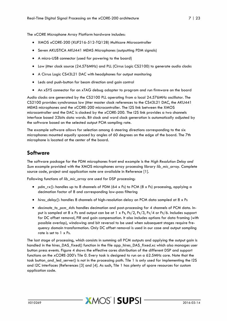
The xCORE Microphone Array Platform hardware includes:
XMOS xCORE-200 (XUF216-512-TQ128) Multicore Microcontroller
Seven AKUSTICA AKU441 MEMS Microphones (outputting PDM signals)
A micro-USB connector (used for powering to the board)
Low jitter clock source (24.576MHz) and PLL (Cirrus Logic CS2100) to generate audio clocks
A Cirrus Logic CS43L21 DAC with headphones for output monitoring
Leds and push-button for beam direction and gain control
An xSYS connector for an xTAG debug adapter to program and run firmware on the board
Audio clocks are generated by the CS2100 PLL operating from a local 24.576MHz oscillator. The
CS2100 provides synchronous low jitter master clock references to the CS43L21 DAC, the AKU441
MEMS microphones and the xCORE-200 microcontroller. The I2S link between the XMOS
microcontroller and the DAC is clocked by the xCORE-200. The I2S link provides a two channels
interface based 32bits data words. Bit clock and word clock generation is automatically adjusted by
the software based on the selected output PCM sampling rate.
The example software allows for selection among 6 steering directions corresponding to the six
microphones mounted equally spaced by angles of 60 degrees on the edge of the board. The 7th
microphone is located at the center of the board.
Software
The software package for the PDM microphones front end example is the High Resolution Delay and
Sum example provided with the XMOS microphones array processing library lib_mic_array. Complete
source code, project and application note are available in Reference [1].
Following functions of lib_mic_array are used for DSP processing:
pdm_rx(): handles up to 8 channels of PDM (64 x Fs) to PCM (8 x Fs) processing, applying a
decimation factor of 8 and corresponding low-pass filtering
hires_delay(): handles 8 channels of high-resolution delay on PCM data sampled at 8 x Fs
decimate_to_pcm_4ch: handles decimation and post-processing for 4 channels of PCM data. In-
put is sampled at 8 x Fs and output can be at 1 x Fs, Fs/2, Fs/3, Fs/4 or Fs/6. Includes support
for DC offset removal, FIR and gain compensation. It also includes options for data framing (with
possible overlap), windowing and bit reversal to be used when subsequent stages require fre-
quency domain transformation. Only DC offset removal is used in our case and output sampling
rate is set to 1 x Fs.
The last stage of processing, which consists in summing all PCM outputs and applying the output gain is
handled in the hires_DAS_fixed() function in the file app_hires_DAS_fixed.xc which also manages user
button press events. Figure 4 shows the effective cores distribution of the different DSP and support
functions on the xCORE-200’s Tile 0. Every task is designed to run on a 62.5MHz core. Note that the
task button_and_led_server() is not in the processing path. Tile 1 is only used for implementing the I2S
and I2C interfaces (References [3] and [4]. As such, Tile 1 has plenty of spare resources for custom
application code.

Real-Time Digital Signal Processing on the xCORE-200 architecture 8 | 23
X010269 2016-03-14
Figure 4: xCORE-200 Tile 0 cores distribution for HiRes Delay and Sum example
Compile-time configuration of the Decimator and Post-Processing stages is done by the
decimator_config_common dcc and decimator_config dc[2] variables at the beginning of the function
hi_res_DAS_fixed() in file app_hires_DAS_fixed.xc. In particular, the frame_size_log2 field of dcc is set
to 0 indicating a frame size of one sample, which results in Sample by Sample Based (SSB) operation
at the output. This provides minimum processing latency which can be very important for voice
applications.
The software provides user run-time control of output gain and steering direction through the buttons
available on the xCore-200 Microphone Array Platform hardware as shown in Table 1.
Button Function
A Rotates steering direction (clockwise)
B Decreases output gain
C Increases output gain
D Rotates steering direction (anti-clockwise)
Table 1: Run-time control of PDM microphones front end example

Real-Time Digital Signal Processing on the xCORE-200 architecture 9 | 23
X010269 2016-03-14
DSP Analysis Context
In order to be representative of real-world performance, a DSP analysis should not be limited to pure
number crunching efficiency. Assessment of computing capabilities on standard algorithms such as FIR
filtering is of course important but system-level features such as data input/output and overall latency
must also be considered.
Keeping front end processing latency as low as possible is a key requirement in many voice interface
applications (especially those featuring bi-directional communication) to enable a natural speech
experience. This raises the question of Block Based (BB) versus Sample by Sample Based (SSB)
processing implementation which will be discussed in more details later in this document.
In terms of audio performances, the complete DSP processing chain should be fully transparent with
respect to the microphones. In other words, the algorithms should exhibit Signal to Noise Ratio (SNR)
and Total Harmonic Distortion plus Noise figures largely exceeding the specifications of the
microphones. Regarding SNR, Reference [5] specifies an SNR of 63dB with a flat frequency response
from 50Hz to 14kHz. One has to consider that 8 microphones are used and each doubling of the
microphones number can provide an SNR increase of 3dB. Hence a global SNR of 72dB should be
considered for the microphones. At least 20dB of excess margin should be considered to accommodate
for the non-flat frequency response of the microphones at the lower and upper end of the audio
spectrum. Table 2 summarizes the audio performance requirements of the PDM microphones front end,
considering a PDM sampling rate of 3.072MHz and a PCM output rate of 48kHz.
Item Value Remarks
Bandwidth 20Hz to 19kHz Largely exceeds voice bandwidth
SNR >= 100 dB Largely exceeds microphones capabilities
THD+N <= 0.002% Low distortion processing
Table 2: Audio performance requirements
The core distribution of the DSP processing implementation is illustrated in Figure 4 and each task is
designed to fit into a 62.5MHz core. In the following chapters, we review key elements of the PDM
microphones DSP front end implementation on xCORE-200. Some comparisons with a standard DSP
architecture (Reference [6]) are also included.
The analysis will be focused on three main topics:
Computations: covers the number crunching capabilities of the xCORE-200 architecture
Latency: analyzes implementation options for achieving lowest latency
Data I/O: reviews system-level integration in terms of data input/output

Real-Time Digital Signal Processing on the xCORE-200 architecture 10 | 23
X010269 2016-03-14
Analysis of Computation Capabilities
Computation capabilities of a DSP system are mainly governed by three factors:
Arithmetic features
Memory access capabilities
Instructions throughput and parallelism
We first review each of these in terms of architecture resources and then in the context of a practical
implementation.
Arithmetic features
The arithmetic features of the xCORE architecture are covered in details in Reference [7].Note that
Reference [7] is based on the first generation xCORE, hence some new features of the xCORE-200
architecture are not covered such as double word load and store. Reference [8] provides a complete
description of the xCORE-200 architecture and related instruction set for the interested reader. We
here just briefly recall the main features of the xCORE-200 ALU:
32 bits integer ALU supporting both signed and unsigned data
Support for single cycle 32 bits x 32 bits -> 64 bits multiply-accumulate (MACCS/MACCU)
Single cycle double word saturation (LSAT) and word extraction (LEXTRACT)
Powerful single cycle bits and bytes manipulation instructions such as BITREV, BYTEREV or
ZIP/UNZIP
Various specialized instructions for CRC computations, divisions, masks generation and others
One of the main features of the xCORE-200 ALU is the single cycle, full precision multiply-accumulate
operation producing 64bits results. This for instance ensures full precision in the computation of FIR
filters without rounding. As such, the xCORE-200 ALU integrates the key requirements for efficient DSP.
Two elements distinguish the xCORE ALU from the ALU of a standard such as the one DSP described in
Reference [6]: SIMD (Single Instruction Multiple Data) support and floating point support. SIMD allows
for parallel processing on multiple data using parallel ALUs executing the same instruction. The xCORE-
200 architecture balances the lack of SIMD support by multiple threads. Using two threads processing
different data streams can be used to emulate SIMD operation.
Lack of native floating point support may render implementation of some algorithms more time
consuming as proper data scaling needs to be verified at each stage to maximize dynamic range. In
most cases this should not be a major issue for experienced DSP. In addition, if properly designed,
fixed point implementations of algorithms often outperform their floating point counterpart (for the
same word-width). This is due to limited effective mantissa precision in floating point formats which is
actually limited to 25bits for a 32bits number. Hence lack of native floating point support is not
considered as a significant drawback of the xCORE-200 architecture in terms of DSP.
Finally, one has to consider that some DSPs (including the one of Reference [6]) integrate dedicated
hardware accelerators for specific DSP tasks such as FIR or IIR filtering and FFT computations. These
clearly give the DSP architecture an advantage over the xCORE-200 architecture in terms of raw
computing power. This advantage could be balanced out by considering an xCORE-200 device with
additional tiles. However, considering the smart interfaces applications space, it is unlikely that the kind

Real-Time Digital Signal Processing on the xCORE-200 architecture 11 | 23
X010269 2016-03-14
of added performance provided by dedicated hardware accelerators are needed in real-world
situations.
Memory access capabilities
Single cycle memory access on the xCORE-200 architecture is supported for both single words (32 bits)
and double words (64 bits). Double word memory access is a new feature of xCORE-200 and was not
supported by the first generation XMOS architecture. In addition, memory access instructions for byte
(8 bits) or short words (16 bits) are also supported.
Following single word data load and store instructions are supported in the xCORE-200:
LDW / STW: load/store based on an address base and offset provided by two registers
(R0…R11)
LDWI / STWI: load/store based on an address base provided by a register (R0…R11) and an
immediate offset in the range (0…11)
LDWCP: load based on the Constant Pool pointer (CP) and a 16bits immediate value
LDWCPL: load based on the Constant Pool pointer (CP) into R11 based on a 20bits immediate
value
LDWDP / STWDP: load/store based on the Data pointer (DP) and a 16bits immediate value
LDWSP / STWSP: load/store based on the Stack pointer (SP) and a 16bits immediate value
Given the large range of immediate values that can be used with these instructions, access to large
buffers can be achieved without requiring additional arithmetic for address computations (clearly at the
price of inflating code size; however for reasonable sizes used in typical filters, up to a few hundred
taps, code size inflation should not be a major issue). Memory accesses as offset from different “non-
computing” registers (CP, DP and SP) allows for access to different buffers with minimal address
generation overhead.
Double word data loads and stores provide double the memory throughput but are supported by a
smaller number of instructions:
LDD / STD: load/store based on an address base and offset provided by two registers
(R0…R11)
LDDI / STDI: load/stores based on an address base provided by a register (R0…R11) and an
immediate offset in the range (0…11)
LDDSP / STDSP: load/store based on the Stack pointer (SP) and an immediate value in the
range (0…. 11)
The choice of instructions for double word access is clearly more limited than the choice for single word
accesses. In addition, memory alignment to 64 bits boundaries must be observed. One also has to be
aware that immediate values have only a short range (0 … 11) which implies that the core may have
to execute additional address generation instructions. As only the stack pointer (SP) is available as
base register other than R0 ... R11, double word access to multiple buffers (for instance state buffer,
stack buffer and/or coefficients buffer) requires temporary load/store of the base addresses or
reservation of some registers. Given the small number of general purpose registers available, it is
unlikely that all bases can be stored without load/store from/to memory.

Real-Time Digital Signal Processing on the xCORE-200 architecture 12 | 23
X010269 2016-03-14
Comparing memory access capabilities of the xCORE-200 and a standard DSP reveals three main
differences:
The standard DSP architecture includes multiple internal busses (typically one for instructions
fetch and one or more for data access). In addition, compute and memory access can be execut-
ed concurrently in the same cycle. Although the xCORE-200 architecture supports dual instruction
issue under certain circumstances, higher clock rates and double word load instructions, the com-
bined throughput of computation and memory access is about half that of a standard DSP core.
As an indication, a typical DSP has two 64 bits busses for data fetches that can access memory
at each processor cycle in parallel with SIMD execution of computations in the ALUs.
Integrated support for circular buffers. Standard DSPs include hardware support for circular
buffers, freeing the code from buffer index management tasks. This is accomplished using special
address generation registers ADDR which are automatically updated at each access according to
ADDR(n+1) = BASE + ((ADDR(n) + STEP) MODULO LENGTH)
where BASE is the base address of the buffer, LENGTH is its length and STEP is the address in-
crement. Lack of integrated support for circular buffers is one of the main drawbacks of the
xCORE-200 architecture in terms of DSP. However, the wide range of memory access functions
based on immediate offsets and some simple tricks as the one detailed in the FIR implementation
example below reduce the impact of lack of native circular buffer support.
Direct Memory Access (DMA) engine. A DMA engine is an integrated hardware resource pre-
sent in most modern DSP which allows for memory to memory transfers to be executed without
core intervention, except for a few instructions required to configure the desired memory trans-
fer. The xCORE-200 architecture does not include a DMA engine but such an engine could easily
be emulated by dedicating one or more thread to memory transfer tasks.
Instructions throughput and parallelism
Throughput and parallel execution of instructions are important factors for the estimation of effective
DSP capabilities as they define the number of instructions that are executed every clock cycle.
In terms of throughput, both the xCORE-200 and standard DSP architecture provide single cycle
execution for the vast majority of instructions. In addition, both have a large unified single cycle access
memory. Hence a throughput of 1 instruction per clock cycle is a reasonable assumption for practical
applications on both platforms.
Instructions parallelism is available on the xCORE-200 using Dual Issue feature of the architecture’s
execution pipeline. There are two Lanes in the xCORE-200 execution pipeline:
The Memory Lane which can execute all memory instructions, branches and basic arithmetic
The Resources Lane which can execute all resources instructions and basic arithmetic
Each thread can chose to execute in Dual Issue mode under control of the programmer, in which case
the processor will execute two 16-bit instructions or a single 32-bit instruction in parallel a single thread
cycle. In dual issue mode, all instructions must be aligned: 32-bit instructions must be 32-bit aligned and
pairs of 16-bit instructions must be aligned on a 32-bit boundary. In addition, destination operands of
parallel executed instructions must be disjoint. This sets some limits on the effective use of Dual Issue and
requires purposely crafted code. In best case situations, the Dual Issue feature of the xCORE-200
allows for a throughput of 2 instructions per clock cycle.

Real-Time Digital Signal Processing on the xCORE-200 architecture 13 | 23
X010269 2016-03-14
On a standard DSP, instructions parallelism is supported by a wide range of architectural features:
Concurrent arithmetic and memory access operations
Multiple busses for concurrent instruction and data fetch
SIMD architecture for concurrent execution of the same instruction on multiple data
Peripheral processor for handling all data I/O without core intervention (through DMA engine)
Accelerators for core off-loading for FIR, IIR and FFT algorithms
Optimal use of all parallelism features of a standard DSP requires careful programming but
throughputs of 16 instructions (or more) per clock cycles can be achieved. Whilst this figure may seem
high compared to what’s achievable on the xCORE-200 architecture, one has to bear in mind that the
DSP architecture is purposely designed to achieve instructions parallelism. However, this is partly offset
by the xCORE-200’s higher clock rate, reducing the throughput ratio advantage for the DSP
architecture from a factor 8 to a factor 4.
Practical processing
We will now look in more details at two of the basic building blocks of the PDM microphone front end,
namely the high-speed first stage filter acting on the PDM inputs and implemented in the pdm_rx()
thread and the second stage FIR filter used to decimate PCM data by four from 384kHz to 96kHz in
the decimate_to_pcm_4ch() task.
pdm_rx() high-speed filter
The pdm_rx() task receives up to 8 channels of PDM data sampled at 3.072MHz and applies a 48
taps FIR filter to perform low-pass filtering and decimation by a factor 8 to produce 32 bits PCM data
at 384kHz. This task operates at a high rate of 384kHz and a brute force implementation of FIR
filtering would require 8 x 48 x 384’000 = 147’456’000 multiply-accumulate operations. If we add
the instructions required for data and coefficients access, close to 300MIPS would be needed (assuming
2 cycles per FIR tap which is realistic as coefficients can be shared across channels). Nevertheless this is
a high figure and would require about 5 cores running at 62.5MHz on the xCORE-200 architecture).
Clearly, a more clever approach would be of benefit. Fortunately, the input data to this high speed
filtering stage is binary Pulse Density Modulated data, meaning that each sample can only take two
values: 0 or 1. Let’s consider an N tap FIR with coefficients ai and assume that N is a multiple of 8. We
can rewrite the time domain equation of the FIR as follows:
𝑦(𝑛) = ∑ 𝑥(𝑛 − 𝑖)𝑎𝑖 = ∑ ∑ 𝑥(𝑛 − (8𝑖 + 𝑗))𝑎8𝑖+𝑗
7
𝑗=0
𝑁8
−1
𝑖=0
𝑁−1
𝑖=0
As x is a binary signal, the inner sum in the above equation can only take 256 different values and can
thus be replaced by a table look-up indexed by the vector (x(n − 8i − 7), … , x(n − 8i)) for i =
0 …N
8− 1. This reduces the number of operations from N multiply-accumulate to
N
8 table look-ups and
additions. The price paid for the drastic reduction in computations is a significant increase in coefficients
memory. Whereas the straight FIR implementation uses N 32bits filter coefficients, the fast
implementation requires storage for N
8 × 256 = 32N pre-computed values (of 32 bits each).

Real-Time Digital Signal Processing on the xCORE-200 architecture 14 | 23
X010269 2016-03-14
The pdm_rx() thread implements the fast FIR algorithm for a 48 taps filter on 8 channels of PDM data
sampled at 3.072MHz on single core running at 62.5MHz. As this filter also applies decimation by a
factor 8, the effective operation rate of the FIR can be reduced to 384kHz. This results in about 20
instructions per output sample. However, for each of the filter’s 6 bins, at least 4 instructions are
required:
Data byte read
Look-up table address generation (add data byte to table base)
Look-up table read
Accumulation
In addition it requires shifting of the bins delay line, input data formatting and general overhead. This
represents 30+ instructions and hence the benefits of the Dual Issue feature of the xCORE-200
architecture for real-time DSP are demonstrated.
The major drawback of the fast FIR algorithm is its significant need of storage memory for pre-
computed look-up tables. For a 48 taps FIR, this results in 48/8 x 256 = 1.5k 32bits storage locations.
The XMOS xCORE-200 support special instructions which allow for halving storage requirements at the
price of a minimal increase in MIPS. The considered FIR being linear phase, its coefficients are
symmetric. Hence if bit reversal is applied between the central bins of the delay line as illustrated in
Figure 5, look-up in the same table can be reused and half of the storage space saved. The required
bit reversal is efficiently implemented on the xCORE-200 architecture using BITREV and BYTEREV
instructions.
Figure 5: Modified fast FIR algorithm for reduced memory requirements
The fast FIR algorithm trades-off computations for random (or, more precisely, input signal related)
memory accesses in the look-up tables and simple additions. As such it can be considered as
representative of the category of random memory access intensive algorithms.
Implementation on a standard DSP of the fast FIR algorithm results in about the same MIPS load. The
dual issue advantage of the xCORE architecture is offset by the larger number of registers of the DSP
architecture which allows computing multiple outputs at once. However, SIMD cannot be used as this
would require multi-offset address accesses in the table look-up phase. Integrating CPU clock rates into
the picture, typically 1’000MHz for a 16 cores xCORE device vs 450MHz for a DSP, even results in an
Real-Time Digital Signal Processing on the xCORE-200 architecture 15 | 23
X010269 2016-03-14
overall efficiency advantage for the XMOS architecture for the implementation of the fast FIR
algorithm. Implementation of the fast FIR algorithm in Assembler and complete characterization of the
48 taps FIR filter are available in Reference [1].
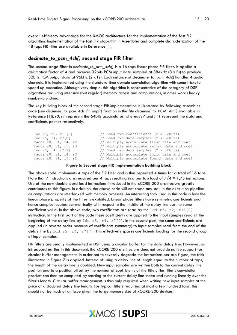
decimate_to_pcm_4ch() second stage FIR filter
The second stage filter in decimate_to_pcm_4ch() is a 16 taps linear phase FIR filter. It applies a
decimation factor of 4 and receives 32bits PCM input data sampled at 384kHz (8 x Fs) to produce
32bits PCM output data at 96kHz (2 x Fs). Each instance of decimate_to_pcm_4ch() handles 4 audio
channels. It is implemented using the standard time domain convolution algorithm with some tricks to
speed up execution. Although very simple, this algorithm is representative of the category of DSP
algorithms requiring intensive (but regular) memory access and computations, in other words heavy
number-crunching.
The key building block of the second stage FIR implementation is illustrated by following assembler
code (see decimate_to_pcm_4ch_fir_impl() function in the file decimate_to_PCM_4ch.S available in
Reference [1]). r0, r1 represent the 64bits accumulator, whereas r7 and r11 represent the data and
coefficients pointer respectively.
ldd r3, r2, r11[0] // Load two coefficients (2 x 32bits)
ldd r5, r4, r7[0] // Load two data samples (2 x 32bits)
maccs r0, r1, r4, r2 // Multiply accumulate first data and coef
maccs r0, r1, r5, r3 // Multiply accumulate second data and coef
ldd r5, r4, r7[7] // Load two data samples (2 x 32bits)
maccs r0, r1, r4, r3 // Multiply accumulate third data and coef
maccs r0, r1, r5, r2 // Multiply accumulate fourth data and coef
Figure 6: Second stage FIR implementation building block
The above code implements 4 taps of the FIR filter and is thus repeated 4 times for a total of 16 taps.
Note that 7 instructions are required per 4 taps resulting in a per tap load of 7/4 = 1,75 instructions.
Use of the new double word load instructions introduced in the xCORE-200 architecture greatly
contributes to this figure. In addition, the above code will not cause any stall in the execution pipeline
as computations are interleaved with memory accesses. An interesting trick used in this code is how the
linear phase property of the filter is exploited. Linear phase filters have symmetric coefficients and
hence samples located symmetrically with respect to the middle of the delay line use the same
coefficient value. In the above code, two coefficients are read by the ldd r3, r2, r11[0]
instruction. In the first part of the code these coefficients are applied to the input samples read at the
beginning of the delay line by ldd r5, r4, r7[0]. In the second part, the same coefficients are
applied (in reverse order because of coefficients symmetry) to input samples read from the end of the
delay line by ldd r5, r4, r7[7]. This effectively spares coefficients loading for the second group
of input samples.
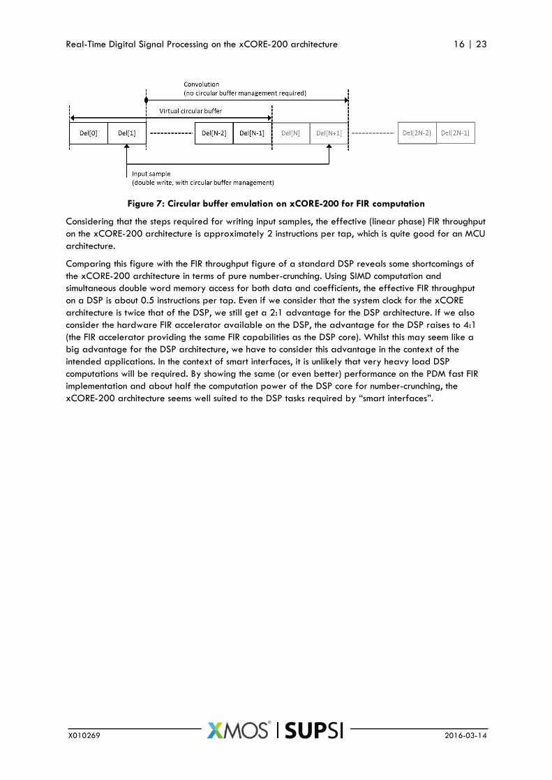
FIR filters are usually implemented in DSP using a circular buffer for the data delay line. However, as
introduced earlier in this document, the xCORE-200 architecture does not provide native support for
circular buffer management. In order not to severely degrade the instructions per tap figure, the trick
illustrated in Figure 7 is applied. Instead of using a delay line of length equal to the number of taps,
the length of the delay line is doubled. New input samples are written both to the current delay line
position and to a position offset by the number of coefficients of the filter. The filter’s convolution
product can then be computed by starting at the current delay line index and running linearly over the
filter’s length. Circular buffer management is thus only required when writing new input samples at the
price of a doubled delay line length. For typical filters requiring at most a few hundred taps, this
should not be much of an issue given the large memory size of xCORE-200 devices.
Real-Time Digital Signal Processing on the xCORE-200 architecture 16 | 23
X010269 2016-03-14
Figure 7: Circular buffer emulation on xCORE-200 for FIR computation
Considering that the steps required for writing input samples, the effective (linear phase) FIR throughput
on the xCORE-200 architecture is approximately 2 instructions per tap, which is quite good for an MCU
architecture.
Comparing this figure with the FIR throughput figure of a standard DSP reveals some shortcomings of
the xCORE-200 architecture in terms of pure number-crunching. Using SIMD computation and
simultaneous double word memory access for both data and coefficients, the effective FIR throughput
on a DSP is about 0.5 instructions per tap. Even if we consider that the system clock for the xCORE
architecture is twice that of the DSP, we still get a 2:1 advantage for the DSP architecture. If we also
consider the hardware FIR accelerator available on the DSP, the advantage for the DSP raises to 4:1
(the FIR accelerator providing the same FIR capabilities as the DSP core). Whilst this may seem like a
big advantage for the DSP architecture, we have to consider this advantage in the context of the
intended applications. In the context of smart interfaces, it is unlikely that very heavy load DSP
computations will be required. By showing the same (or even better) performance on the PDM fast FIR
implementation and about half the computation power of the DSP core for number-crunching, the
xCORE-200 architecture seems well suited to the DSP tasks required by “smart interfaces”.

Real-Time Digital Signal Processing on the xCORE-200 architecture 17 | 23
X010269 2016-03-14
Latency Analysis
As already introduced earlier in this document, low latency is an important requirement for voice
interfaces. Latency is highly dependent on the effective processing architecture. There are two main
approaches to implementing real-time DSP processing systems:
Block Based (BB): In a BB system, blocks of 2^M samples (M = 5 to 8 typically) are processed at
once. New input data is buffered and processing is fired once the correct number of samples has
been received. This clearly introduces a minimal latency equal to the block length of the system.
Sample by Sample Based (SSB): In a SSB system, processing is fired for every input sample (or
for every small number of them). This requires no (or only minimal) buffering at I/O level and
between processing cores, resulting in minimal input to output latency (excluding any latency in-
herent to the processing algorithms).
Figure 8 illustrates BB and SSB processing architectures whereas Table 3 provides a comparison of
some key features of both architectures.
Figure 8: DSP processing architectures (BB top, SSB bottom)
Feature Block Based (BB) Sample by Sample Based (SSB)
Operating princi-ple
Cores compute DSP algorithms on blocks of data (typically 2^M samples, across 1 or more channels). Data is transmitted from core to core by references to data buffers in global memory.
Typical software (RTOS) approach.
Cores compute DSP algorithms on individ-ual data samples (possibly several chan-nels at once). Data is transmitted directly from core to core and availability of new data fires processing (event driven).
This is similar to a hardware processing line controlled by host supervisor

Real-Time Digital Signal Processing on the xCORE-200 architecture 18 | 23
X010269 2016-03-14
Feature Block Based (BB) Sample by Sample Based (SSB)
Basic data pro-cessing unit and processing rate
Data block of 2^M samples
Algorithms are called at the rate of Fs/(2^M) where Fs is the signal’s sampling rate
Single (or very low number of) sample(s)
Algorithms are typically called at the rate of Fs, where Fs is the signal’s sampling rate
Latency A minimal latency of 2^M samples is intro-duced by BB processing (excluding any delay intrinsic to the DSP algorithms).
However a latency of 2^M samples can be difficult to achieve due to multiple buffering, typically at I/O level. Hence it is more reasonable to consider a delay of B x 2^M samples (B = 4 typical)
SSB approach allows for minimal signal path latency (excluding any delay intrinsic to the DSP algorithms).
Typical latencies of only a few samples can be achieved.
Processing over-head
Any overhead due to run-time algorithms setup is spread over 2^M samples. Hence, considering an overhead of C cycles for algorithms run-time setup, its effective contribution to the total load per sample is C / (2^M) cycles.
Any overhead due to run-time algorithms setup must be considered for each sample. Hence its contribution to the total load per sample is C cycles.
It is therefore crucial that algorithms run-time setup be kept to a minimum.
Control Control of DSP algorithms is typically han-dled by the same core as the real-time execution of the algorithm.
Nevertheless, for control functions involving complex computations (such as filter coef-ficients computations), implementation in an asynchronous task may be required.
Control of DSP algorithms is typically han-dled by a different core and is handled asynchronously.
Separation of real-time and non-real-time parts is crucial in SSB processing.
Table 3: Comparison of BB and SSB processing
Given its event-driven architecture and channels-based inter-core communication infrastructure, the
xCORE-200 architecture is well suited to SSB processing. Channels provide efficient pipes to pass data
from one core to the other in a deterministic, low latency manner. Considering that both PDM input and
PCM output ports are implemented using buffered ports (introducing between 1 and 2 samples of
delay) and that both consumer and producer ends of a channel between processing cores introduce a
one sample delay, overall system latency can be estimated as show in Table 4 (for an output sampling
rate of 48kHz and excluding any latency inherent to the algorithms). An important point to notice about
SSB processing on the xCORE-200 architecture is that overhead for context switch is quite limited due
to the small number of registers to store/recall. About 20 instructions are required, which represent
about 1 MIPS at a sampling rate of 48kHz.
Item Latency Remarks
Input port 1/96 to 2/96 ms Buffered port. Latency corresponds to 32 to 64 symbols at 3.072MHz (symbols are grouped in 32bits words)
Consumers/Producers
(channels)
8 x 1/48 ms Processing path contains 4 channels in series. Each consum-er/producer introduces a latency of one sample at 48kHz.
Output port 1/48 ms Buffered port. Latency is at most one sample at 48kHz as output is I2S which is a stereo stream
Total < 0.21 ms System latency. Does not include latency inherent to the processing algorithms.
Table 4: xCORE-200 system latency of PDM microphones front end
Real-Time Digital Signal Processing on the xCORE-200 architecture 19 | 23
X010269 2016-03-14
For comparison, assuming a BB implementation on a standard DSP with a block length of 64 samples
(M = 6) and several stages of buffering (B = 4), minimal overall system latency would be equal to 64
x 4 / 48 = 5.33 ms. SSB implementation would of course be possible on a standard DSP but overhead
due to context switch may become a limiting factor as a large number of registers have to be
saved/restored (including computation registers, data address generator registers and general
configuration registers). Typical context switches on modern DSPs may require between 50 and 100
instructions. In order to speed up context switches, some DSP architectures (such as ADSP-2148x) include
a set of shadow registers which can be swapped with the main registers. However, this solution only
allows for fast context switch between 2 contexts, corresponding to the main and shadow registers
respectively. Any switch between more than 2 contexts would still be affected by high overhead. In
addition, I/O ports of standard DSPs typically include small FIFOs of a few samples which would add
up to overall latency.
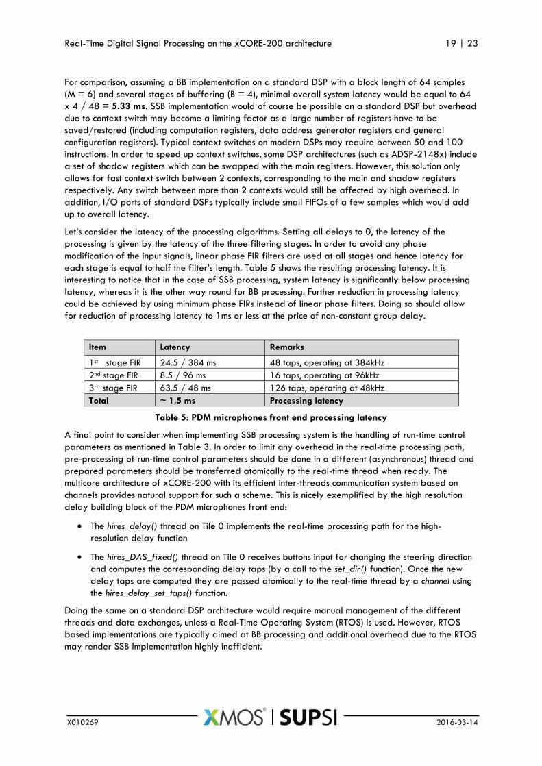
Let’s consider the latency of the processing algorithms. Setting all delays to 0, the latency of the
processing is given by the latency of the three filtering stages. In order to avoid any phase
modification of the input signals, linear phase FIR filters are used at all stages and hence latency for
each stage is equal to half the filter’s length. Table 5 shows the resulting processing latency. It is
interesting to notice that in the case of SSB processing, system latency is significantly below processing
latency, whereas it is the other way round for BB processing. Further reduction in processing latency
could be achieved by using minimum phase FIRs instead of linear phase filters. Doing so should allow
for reduction of processing latency to 1ms or less at the price of non-constant group delay.
Item Latency Remarks
1st stage FIR 24.5 / 384 ms 48 taps, operating at 384kHz
2nd stage FIR 8.5 / 96 ms 16 taps, operating at 96kHz
3rd stage FIR 63.5 / 48 ms 126 taps, operating at 48kHz
Total ~ 1,5 ms Processing latency
Table 5: PDM microphones front end processing latency
A final point to consider when implementing SSB processing system is the handling of run-time control
parameters as mentioned in Table 3. In order to limit any overhead in the real-time processing path,
pre-processing of run-time control parameters should be done in a different (asynchronous) thread and
prepared parameters should be transferred atomically to the real-time thread when ready. The
multicore architecture of xCORE-200 with its efficient inter-threads communication system based on
channels provides natural support for such a scheme. This is nicely exemplified by the high resolution
delay building block of the PDM microphones front end:
The hires_delay() thread on Tile 0 implements the real-time processing path for the high-
resolution delay function
The hires_DAS_fixed() thread on Tile 0 receives buttons input for changing the steering direction
and computes the corresponding delay taps (by a call to the set_dir() function). Once the new
delay taps are computed they are passed atomically to the real-time thread by a channel using
the hires_delay_set_taps() function.
Doing the same on a standard DSP architecture would require manual management of the different
threads and data exchanges, unless a Real-Time Operating System (RTOS) is used. However, RTOS
based implementations are typically aimed at BB processing and additional overhead due to the RTOS
may render SSB implementation highly inefficient.

Real-Time Digital Signal Processing on the xCORE-200 architecture 20 | 23
X010269 2016-03-14
Data I/O Analysis
Data I/O and formatting is also an important point when considering the overall DSP capabilities of a
system. For instance, in a typical voice beam forming application 8, 16 or even up to 32 microphones
may be used, each requiring an input to the DSP system.
With its fully configurable I/O ports, the xCORE-200 architecture provides a flexible interface which
can easily be adapted to a particular use case. Let’s consider the PDM input of the example PDM Hires
Sum and Delay application with its 8 channels of PDM input. Data from the PDM microphones is
acquired through an 8bits buffered port formatting its data into 32bits word by stuffing successive
groups of input samples. However, this format is not suitable for the fast FIR filtering stage in pdm_rx()
and input data formatting is required as shown in Figure 9.
Figure 9: PDM input data formatting
Given that data received from the input port are 32bits words, each containing 4bits from each of the
8 input channels, the effective input event rate is 3.072MHz / 4 = 768kHz. Considering that input data
formatting is required at this rate, a highly efficient implementation is required to keep overhead within
bounds. The UNZIP instruction of the xCORE-200 architecture provides an elegant solution as shown in
the code snippet of Figure 10. These three instructions are enough to re-order two 32bits input words
(a and b respectively) of time domain multiplexed inputs into bytes containing the successive PDM
samples for a given channel. Considering that 2 input samples are handled at once, the effective CPU
load is only 3 instructions at 384kHz (which is less than 1.2 MIPS).
unzip a, b, 2 // Assemble nibbles (groups of 4 channels data)
unzip a, b, 1 // Assemble bit-pairs (groups of 2 channels data)
unzip a, b, 0 // Assemble single bits (groups of 1 channel data)
Figure 10: Efficient input data formatting implementation
The output side of the example application uses a standard I2S port operating in master mode. This
component is part of the base library of the xCORE-200 platform. Clocks for the I2S port are
generated by the library from the audio master clock input. The I2S port is a good example of
software based implementation of hardware functions, typical of the xCORE architecture. Being
Real-Time Digital Signal Processing on the xCORE-200 architecture 21 | 23
X010269 2016-03-14
implemented in software, the I2S port clearly steels some resources from the cores which could have
been used for DSP or other processing/control functions; however, the overall impact remains small (see
Reference [3] for more details).
If we consider the case of standard DSPs, their architecture include a large count and variety of
peripherals such as multiple serial ports (including I2S support), I2C or SPI ports for control, GPIOs,
clock generators and PWM generators among others. Serial ports can easily be configured to receive
PDM inputs, for instance by acquiring 32bits words containing successive PDM samples of a given
channel. Doing so ensures that received data is in the right format for the fast FIR algorithm. Assignment
of peripherals and core I/Os to the pins of the DSP is done through programmable Signal Routing Units
(SRUs). These provide zero-overhead, flexible routing of I/O signals. Some constraints on the SRUs
(mainly linked to the number of freely assignable pins) may limit system integration when large
numbers of I/O signals are considered. As such, the flexibility provided by the software based
approach to I/O ports configuration and implementation of the xCORE-200 architecture may turn out
as an advantage when overall system cost is considered.

Real-Time Digital Signal Processing on the xCORE-200 architecture 22 | 23
X010269 2016-03-14
Conclusion
This whitepaper has looked at the DSP capabilities of the recently introduced XMOS xCORE-200
architecture. Several aspects of the platform including number-crunching capabilities, latency and
system integration have been analyzed in the context of a voice interface based on PDM microphones.
A unique feature of the xCORE-200 platform is its natural support of Sample by Sample Based
processing thanks to its multi-threaded, event-driven architecture which allows for practical
implementation of very low latency solutions.
On the DSP computing side, the xCORE-200 shows excellent performance for algorithms requiring
intensive random memory accesses such as the fast FIR algorithm for PDM input data detailed in this
document. On such type of algorithms the xCORE-200 architecture shows similar or even better
performance than dedicated DSP architectures. If compute-intensive algorithms with concurrent regular
memory accesses such as the time-domain convolution implementation of FIR filters are considered, the
advantage clearly goes to dedicated DSP architectures but the xCORE-200 still presents respectable
performance.
Combining the advantages of very low latency, configurability, system-level integration and solid real-
time DSP processing capabilities, the xCORE-200 architecture seems particularly well suited to voice
enabled smart interfaces. For applications based on natural speech interaction (such as connected
assistants or teleconferencing systems), the sub-millisecond latency enabled by Sample by Sample
Based processing is clearly a key advantage of the XMOS platform. In addition, the computing
requirements of such products are in-line with the xCORE-200’s DSP capabilities. Finally, the high level
of system integration provided by the platform’s configurable hardware allows for optimal BOM cost.
Further applications could also benefit from the xCORE-200’s DSP capabilities, in particular the family
of High-Resolution Audio interfaces. High Resolution Audio applications need to support the DSD audio
format, which indeed is a PDM signal. Unfortunately, any signal processing carried out on a DSD
stream (except for a pure delay) will destroy the 1bit nature of the signal. Hence, whenever signal
processing is required, for instance for headphones listening enhancements or 3D audio, DSD has to be
converted to PCM. This could be implemented using the same fast FIR algorithm as used for the PDM
microphones application and run very efficiently on the xCORE-200 architecture.

Real-Time Digital Signal Processing on the xCORE-200 architecture 23 | 23
X010269 2016-03-14
References
1. XMOS lib_mic_array library. The PDM microphone front end considered in this paper is the High
Resolution Delay and Sum example of the library package. Refer to application note AN00218
(https://www.xmos.com/published/an00218-high-resolution-delay-and-sum?version=latest) and
related source code (https://www.xmos.com/published/lib_mic_array-sw?version=latest)
2. PDM microphone platform hardware documentation: xCORE Microphone Array Platform Hardware
Manual (http://www.xmos.com/published/microphone-array-reference-design-hardware-
manual?version=latest)
3. XMOS I2S library (http://www.xmos.com/support/libraries/lib_i2s)
4. XMOS I2C library (http://www.xmos.com/support/libraries/lib_i2c)
5. AKU441 MEMS microphone product brief
(http://www.akustica.com/Files/Admin/PDFs/Product%20Briefs/PB25%2D1%2E0%20%2D%20A
KU441%20Product%20Brief%2Epdf)
6. Analog Devices SHARC ADSP2148x datasheet (http://www.analog.com/media/en/technical-
documentation/data-sheets/ADSP-21483_21486_21487_21488_21489.pdf)
7. Digital Signal Processing on the XCore XS1 for Embedded Developers
(http://www.xmos.com/published/digital-signal-processing-on-the-xcore-xs1-for-embedded-
developers?version=latest)
8. xCORE-200: The XMOS XS2 Architecture ISA (http://www.xmos.com/published/xs2-isa-
specification?version=latest)


![ECE-V-DIGITAL SIGNAL PROCESSING [10EC52] …vtusolution.in/.../digital-signal-processing-10ec52.pdfDigital vtusolution.in Signal Processing 10EC52 TEXT BOOK: 1. DIGITAL SIGNAL PROCESSING](https://img.pdfslide.net/doc/110x75/5afe42bb7f8b9a256b8ccd2e/ece-v-digital-signal-processing-10ec52-signal-processing-10ec52-text-book.jpg)