Embed Size (px)
Citation preview

RECEIVER BANDWIDTH ENHANCEMENT DESIGN FOR HIGH SPEED
OPTICAL SYSTEM
INTAN SHAFINAZ BINTI MOHAMMAD
A project report submitted in partial
fulfilment of the requirement for the award of the
Degree of Master of Electrical Engineering
Faculty of Electrical and Electronic Engineering
Universiti Tun Hussein Onn Malaysia
JULY 2013
v
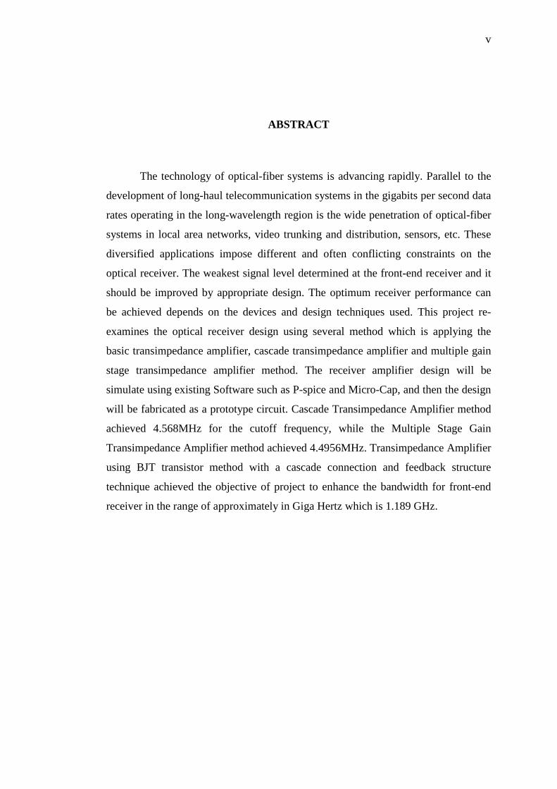
ABSTRACT
The technology of optical-fiber systems is advancing rapidly. Parallel to the
development of long-haul telecommunication systems in the gigabits per second data
rates operating in the long-wavelength region is the wide penetration of optical-fiber
systems in local area networks, video trunking and distribution, sensors, etc. These
diversified applications impose different and often conflicting constraints on the
optical receiver. The weakest signal level determined at the front-end receiver and it
should be improved by appropriate design. The optimum receiver performance can
be achieved depends on the devices and design techniques used. This project re-
examines the optical receiver design using several method which is applying the
basic transimpedance amplifier, cascade transimpedance amplifier and multiple gain
stage transimpedance amplifier method. The receiver amplifier design will be
simulate using existing Software such as P-spice and Micro-Cap, and then the design
will be fabricated as a prototype circuit. Cascade Transimpedance Amplifier method
achieved 4.568MHz for the cutoff frequency, while the Multiple Stage Gain
Transimpedance Amplifier method achieved 4.4956MHz. Transimpedance Amplifier
using BJT transistor method with a cascade connection and feedback structure
technique achieved the objective of project to enhance the bandwidth for front-end
receiver in the range of approximately in Giga Hertz which is 1.189 GHz.
vi
ABSTRAK
Teknologi sistem gentian optik kini semakin berkembang pesat dari hari ke
hari. Selaras dengan perkembangan sistem komunikasi jarak jauh yang mencapai
kadar data gigabit per saat dalam komunikasi serantau, sistem gentian optik kini telah
mula menembusi rangkaian kawasan tempatan, saluran video, pengedaran, pengesan
dan beberapa teknologi lain secara meluas. Kepelbagaian aplikasi telah menimbulkan
pelbagai masalah teknikal dan konflik dalam penerima optik. Penerimaan aras isyarat
yang lemah pada penerima hadapan perlu diperbaiki dengan rekaan teknologi yang
lebih jitu dan sesuai. Keupayaan penerima boleh dicapai secara optimum bergantung
kepada peralatan dan rekabentuk teknik yang digunakan. Projek ini akan mengkaji
semula rekabentuk penerima optik menggunakan beberapa kaedah seperti penguat
transimpedan asas, penguat transimpedan lata dan penguat transimpedan pelbagai
peringkat. Rekabentuk penerima penguat ini disimulasi melalui perisian seperti P-
Spice dan Micro-Cap sebelum difabrikasi kepada litar prototaip. Kaedah Penguat
Lata Transimpedan telah mencapai 4.568MHz untuk ‘cutoff frequency’, manakala
kaedah Penguat Pelbagai Peringkat telah mencapai 4.4956MHz untuk ‘cutoff
frequency’ . Penguat Transimpedan yang dihasilkan menggunakan transistor BJT
dan penyambungan lata (cascade connection) serta teknik struktur suapbalik
(feedback structure technique), berjaya mencapai objektif untuk meningkatkan kadar
jalur lebar penerima hadapan supaya mencapai frekuansi Giga Hertz iaitu 1.189
GHz.

vii
TABLE OF CONTENTS
TITLE i
DECLARATION ii
DEDICATION iii
ACKNOWLEDGEMENT iv
ABSTRACT v
ABSTRAK vi
TABLE OF CONTENTS vii
LIST OF TABLES x
LIST OF FIGURES xi
LIST OF ABBREVIATIONS xiv
LIST OF SYMBOLS xv
LIST OF APPENDICES xvi
CHAPTER 1 INTRODUCTION 1
1.1 Project Background 1
1.2 Problem Statement 2
1.3 Project Objective 3
1.5 Project Scopes 3
viii
1.5 Thesis Outline 5
CHAPTER 2 LITERATURE REVIEW 7
2.1 Basic Concept of Fiber Optic System 7
2.1.1 Architecture of Optical front-End 9
2.1.1.1 Low-impedance Voltage Amplifier 10
2.1.1.2 High-impedance Voltage Amplifier 11
2.1.1.3 Transimpedance Amplifier 12
2.2 Gain Bandwidth Product 14
2.3 Transistor Amplifier Analysis and Small Signal Model 15
2.3.1 Hybrid- π Model 16
2.3.1 T Model 18
2.4 Previous Research Review 20
2.4.1 First Review 20
2.4.2 Second Review 22
2.4.3 Third Review 24
2.4.4 Fourth Review 25
2.5 Summary of Previous Research Review 28
CHAPTER 3 METHODOLOGY 29
3.1 Receiver Front-end Amplifier Simulation And Analysis 29
3.2 Cascade Transimpedance Amplifier (TIA)using LMH6642 30
3.2.1 Mathematical Analysis and Simulation Result 31
for Cascade Transimpedance Amplifier (TIA)
3.3 Multiple Stage Gain Transimpedance Amplifier (TIA) 32
Using LMH6642
3.3.1 Mathematical Analysis and Simulation Result 33
for Multiple Stage Gain Transimpedance Amplifier
3.4 Transimpedance Amplifier(TIA) Using BJT Transistor 34
(BFR540)
ix
3.4.1 Mathematical Analysis and Simulation Result 35
for Transimpedance Amplifier(TIA) Using
BJT Transistor
3.5 Comparing the Simulation Result 40
CHAPTER 4 HARDWARE FABRICATION & EXPERIMENTAL 41
SETUP PROCESS
4.1 Schematic and Layout Design 41
4.2 Printed Circuit Board (PCB) 42
4.3 PCB Developing Process 43
4.4. Etching Process 44
4.5. Experimental Setup 45
CHAPTER 5 TESTING MEASUREMENT OF DEVELOPED CIRCUIT 46
CHAPTER 6 CONCLUSION AND RECOMMENDATION 50
6.1 Recommendations 51
REFERENCE 52
APPENDICES 55

x
LIST OF TABLES
TABLE TITLE PAGE
3.1 Summary table for simulation result 42
5.1 Result for prototype design of Transimpedance 61
Amplifier using BJT transistor.
xi
LIST OF FIGURES
FIGURE TITLE PAGE
1.1 Block diagram of fiber optic system 4
2.1 Block Diagram of a fiber system 8
2.2 Optical Receiver Front-End 10
2.3 AC coupled low-impedance voltage amplifier 11
2.4 High-impedance amplifier 12
2.5 Typical circuit configuration of TIA 13
2.6 The transimpedance feedback amplifier 14
2.7 Simplified response curve where fc1 is negligible 15
(assume to be zero) compare to fcu
2.8 The amplifier circuit with dc source VBE and VCC 17
eliminated (short circuit)
2.9 (a) BJT as a voltage-controlled current source- 18
( a transconductance amplifier)
(b) BJT as a current-controlled current source-
(a current amplifier)
2.10 Hybrid-π Model with the resistance r0 included 19
2.11 (a) BJT as a voltage-controlled current source 20
(b) BJT as a current-controlled current source 20
2.12 Three-stage conventional MA 22
xii
2.13 Topology of the proposed MA 22
2.14 Topology of the uniform 2-stage CMA 23
2.15 (a) Circuit schematic of C-peaking transimpedance 24
amplifier
(b) Equivalent open-loop circuit of transimpedance 24
amplifier with and without a peaking capacitor.
2.16 Frequency Response of Series-Shunt Bootstrap 26
2.17 The op amp based transimpedance amplifier 27
2.18 Frequency response of the op-amp 28
2.19 Shunt bootstrap photodiode preamplifier 29
2.20 Practical frequency responses of the shunt circuit 29
and standard transimpedance amplifier
3.1 Cascade Transimpedance amplifier using LMH6642 32
3.2 Frequency Response for Cascade TIA circuit 33
3.3 Multiple Gain Stage Transimpedance Amplifiers (TIA) 34
3.4 Frequency Response for Multiple Gain Stage TIA circuit 35
3.5 Transimpedance Amplifier (TIA) Used of BJT transistor 37
3.6 Simplified circuit of TIA using Hybrid-π Model 39
3.7 Simplified circuit of TIA with closed loop 40
3.8 Frequency Response for TIA Used of BJT transistor 41
4.1 PCB layout design of the front-end receiver 43
circuit amplifier.
4.2 UV exposure machine 44
4.3 Developing process 44
4.4 Etching machine 45
4.5 PCB circuit of the proposed front-end receiver amplifier 45
4.6 (a) Signal Generator of 9 kHz- 6 GHz 46
(b) Oscilloscope
(c) Power Supply
4.7 Setup for testing circuit 47

xiii
5.1 (a) input waveform at 100kHz 49
(b) output waveform at 100kHz
5.2 Gain versus frequency response 50
5.3 Simulation Result for Frequency Response for 51
TIA Used of BJT transistor
xiv
LIST OF ABBREVIATIONS
BW - Bandwidth
FSO Free Space Optic
GBW - Gain Bandwidth Product
BJT - Bipolar Junction Transistor
Hz - Hertz
PCB - Printed Circuit Board
TIA - Transimpedance Amplifier
dB - Decibel

xv
LIST OF SYMBOLS
GHz - Giga-Hertz
MHz - Mega Hertz
Rf - Feedback capacitor
Cf - Feedback capacitance
- Upper critical frequency
- Lower critical frequency
- Output resistance
- Small-signal input resistance between base and emitter
(Looking into the emitter)
- Small-signal input resistance between base and emitter
(Looking into the base)
- Transconductance
- Total instantaneous base-emitter voltage

xvi
LIST OF APPENDICES
APPENDICES TITLE PAGE
Appendix A1 BFR540 data sheet 56
AppendixA2 LMH6642 datasheet 61
1
CHAPTER 1
INTRODUCTION
1.1 Project Background
The emergence of fiber optic and free space optics (FSO) technologies nowadays has
made it as a base in the communication field, replacing the electrical transmission
medium. This is because of the demand for higher speed and wider bandwidth in a data
communication network. If the fiber optic and FSO system had a bad configuration of
optical receiver, it will cause the system to be slow, noisy and a lot of disturbance. All
potential disturbances and noise can be addressed through the appropriate network
design and planning. The weakest signal level is determined at the front-end receiver
and it should be improved by appropriate design. The optimum receiver performance
can be achieved depends on the devices and design techniques used [1].
A good sensitivity and a broad bandwidth will invariably use a small area
photodiode where the aperture is small. However, free-space optics requires a large
aperture and thus, the receiver is required to have a large collection area, which may be
achieved by using a large area photodetector and large filter. However, large area of
photodetector produces a high input capacitance that will be reduced the bandwidth.
Typical large photodetection area commercial detectors has capacitance are around 100-
300pF compared to 50pF in fiber link. Hence, techniques to reduce the effective detector
capacitance are required in order to achieve a low noise and wide bandwidth design.
2
This project aims to use Transimpedance Amplifier using BJT transistor with a cascade
connection and feedback structure technique, to enhance the bandwidth for front-end
receiver, due to successful storey using this technique by various researcher.
1.1 Problem Statements
The weakest front end means that is too noisy and too slow or both. The performance of
the optical front end receiver has a significant impact on the overall optical system
performance .In order to reduce shot noise in the detector due to ambient light an optical
filter is required, whilst the preamplifier should allow shot-noise limited operation. The
signal level in an optical receiver is weakest at the front end of the receiver due to the
photodetector capacitance. In addition, there are high path loss and background noise in
the environment system.
A fundamental requirement in the design of an optical receiver is the
achievement of high sensitivity and broad bandwidth. There are several basic
configurations such as low-impedance voltage amplifier, high impedance amplifier and
transimpedance amplifier. Any of the configurations can be built using contemporary
electronics devices such as operational amplifiers (Op-Amp), bipolar junction transistors
(BJT), field effect transistors (FET) or high electron mobility transistor (such as
CMOS). The receiver performance that is achieved will depend on the devices and
design techniques used. In this project presented several techniques to broaden the
bandwidth and maximize the receiver performance.
3
1.2 Project Objectives
The objectives of this project are as follows:
a) To improve front-end receiver performance and enhance the receiver bandwidth.
b) To design the receiver amplifier with the bandwidth enhancement in the range of
approximately in Giga hertz using existing Software such as P-spice and Micro-Cap.
c) To develop and fabricate a prototype of the designed receiver amplifier.
1.3 Project Scopes
This project focused on the concept of fiber and wireless optical receiver amplifier
communication. The circuit will be designed to meet the objective of having a receiver
with bandwidth enhancement capabilities. There are several scopes for this project:
a) The main scope concentrates on this project towards the front-end receiver in a red
box, refer to Figure 1.1 below which contains only preamplifier circuit.
b) There are several methods proposed in designing the front-end receiver for this
project to improve receiver performance and bandwidth enhancement to perform
high gain-bandwidth which are the basic transimpedance amplifier, cascade
transimpedance amplifier and multiple gain stage transimpedance amplifier. The
simulation results for each technique will be compared where the best performance
receiver for wider bandwidth and high gain is chosen to be fabricated as prototype.
The proposed design will used of the BJT transistor (BFR540) and amplifier
IC(LMH6642).

4
Figure 1.1: Block diagram of fiber optic system [3]
c) The design of receiver amplifier circuit will be simulate using Micro-cap electronic
software and Orcad P-spice.
d) The output simulation result using P-spice will be compared with the output
prototype circuit to verify the result.

5
1.5 Thesis Outline
This thesis presents an overview study of several application techniques on designing a
front-end optical receiver to improve the receiver performance and bandwidth
enhancement in order to obtain high gain-bandwidth. The summaries of each chapter in
this project are as follows:
Chapter 1
The objectives and scopes for this project are explained in Chapter1.
Chapter 2
This chapter will present the entire concept or technique that has been used by previous
researcher and the theory that will be used in designing this project.
Chapter 3
Chapter 3 will focus on the techniques that will be used in designing this project such as
TIA, cascade and multistage technique. This chapter will also present the simulation
output of the proposed design circuit using Micro-cap software and Orcad Pspice.
Chapter 4
This chapter will focused on the procedure on how to fabricated the prototype circuit.
The fabricated prototype circuit is based on the selected circuit that has been chosen
depending on the simulation result which is discussed in Chapter 3. A brief description
on the equipments used in experimental work and method used for measurement in this
project will be explained in this chapter.
Chapter 5
This chapter discussed the result obtained from experimental test and its practical
measurement is presented here.

6
Chapter 6
All the findings and comparison between software simulation and hardware
measurements will be concluded in this Chapter. A summary of this project will be
discussed, along with future recommendation for further improvement of this work.
7
CHAPTER 2
LITERATURE REVIEW
2.1 Basic Concept of Fiber Optic System
A basic optical communication system is well illustrated in Figure 2.1. This
system basically same with other communication systems, there is a transmitter, a
receiver, and a channel to convey energy from transmitter to receiver. The information
to be transmitted to the receiver is assumed to exist initially in an electrical form. The
information from the transmitter is combined with the drive signals needed to operate a
laser. The laser output is coupled into an optical fiber through which it propagates to the
receiver. The receiver may perform optical processing on the incoming signal. The
optical processing may correspond to a simple optical filter or it may involve
interferometers, the introduction of additional optical fields, or the use of an optical
amplifier. Once the received field is optically processed it is detected. The
photodetection process generates an electrical signal that varies in response to the
modulations present in the received optical field. The electrical signal is typically low-
level and requires amplification and signal processing for the information to be
recovered [4][5].

8
Figure 2.1: Block Diagram of a fiber system [4]
From the previous research, the front-end plays a major role in determining the
noise performance of receiver. This research project tends to focus in designing and
developing the front end-receiver amplifier.

9
2.1.1 Architecture of Optical Front-End
Theoretically, the front-end of an optical receiver responds to an optical signal by
generating a photocurrent with a photodetector. The photocurrent is then converted into
voltage. In order to extract the desired information, the recovered voltage had been
process on the electronic signal processing stages. The dimensions of the transfer
function associated with the front-end will consequently be volts per amp or ohms.
Therefore, the transfer functions of virtually all optical receivers are actually
transimpedance in nature.
Figure 2.2: Optical Receiver Front-End [2].
The configuration of an optical receiver as shown in Figure 2.2 consists of
photodetector which is the fundamental element, followed by amplifiers and signal
conditioning circuitry. The optical receiver will convert the optical energy emerging
from electrical signal and then to amplify the signal to a large enough value, it will be
processed by the electronic circuit following the receiver amplifier.

10
An optical receiver’s front-end design can usually be grouped into three basic
configurations [2]:
a) Low-impedance voltage amplifier
b) High-impedance amplifier
c) Transimpedance amplifier
Any of the configurations can be built using contemporary electronic devices
such as operational amplifiers, bipolar junction transistors, field-effect transistors, or
high electron mobility transistors. The receiver performance that is achieved will
depend on the devices and design techniques used.
2.1.1.1 Low-impedance Voltage Amplifier
A simple optical receiver front-end consists of a photodetector, a load resistor
and a low input-impedance voltage amplifier. The photodiode can be either AC coupled
or DC coupled to the amplifier as shown in Figure 2.3. In the AC coupled amplifier, a
separate load resistor is used to derive a voltage proportional to the photocurrent and to
provide a path for the DC photocurrent to flow. The low-frequency components of the
photocurrent see a load resistor Rl while the high-frequency see a load resistance that is
the parallel combination of Rl and the amplifier input impedance Zin. There are a wide
variety of commercially available high gain wideband amplifiers that are AC coupled.
Figure 2.3: AC coupled low-impedance voltage amplifier [4]
11
2.1.1.2 High-impedance Voltage Amplifier
The high-impedance amplifier is an approach that substantially reduces the effect of the
thermal-noise of the load resistor, resulting improved sensitivity. The high-impedance
receiver is based on a technique that has been successfully used over other capacitive
current sources such as silicon tubes and is descended from vacuum tube amplifiers.
Figure 2.4 shows a simple high-impedance amplifier configuration.
The basic design principle is to load the current-source with as large impedance
as possible. This will maximize the amount of voltage developed at the input of the
amplifier, since the voltage is maximized, the effects of any amplifier noise sources will
be reduced. In general, the high-impedance receiver results in the lowest noise baseband
front-end that can be realized without extraordinary effort where the low-noise is
obtained by making the load resistor as large as possible.
Figure 2.4: High-impedance amplifier [4]
12
2.1.1.3 Transimpedance Amplifier
Bandwidth is a high priority in transimpedance amplifiers (TIA). Unlike conventional
microwave amplifiers, these amplifiers have to maintain an acceptable response down to
very low frequencies and still perform satisfactorily at high frequencies. The low
frequency response must extend as close as possible to zero Hz. This aspect of the
transimpedance amplifiers is usually the primary focus in the design. It is very difficult
to maintain a flat gain versus frequency response at low frequencies when the upper
frequency goes into the GHz region. Device inadequacies and bias networks commonly
limit the lowest achievable frequency.
The transimpedance design uses a feedback to reduce input impedance, where this
will permit fast response due to the low effective input RC-time constant and low
thermal noise since Rf can be made large. The result is that the RC-time constant
limitation is multiplied by the amplifier gain and the signal output is a function of the
size of the feedback resistance. The transimpedance amplifier has a wide range but is
limited in noise performance or frequency response.
Figure 2.5: Typical circuit configuration of TIA [4].
13
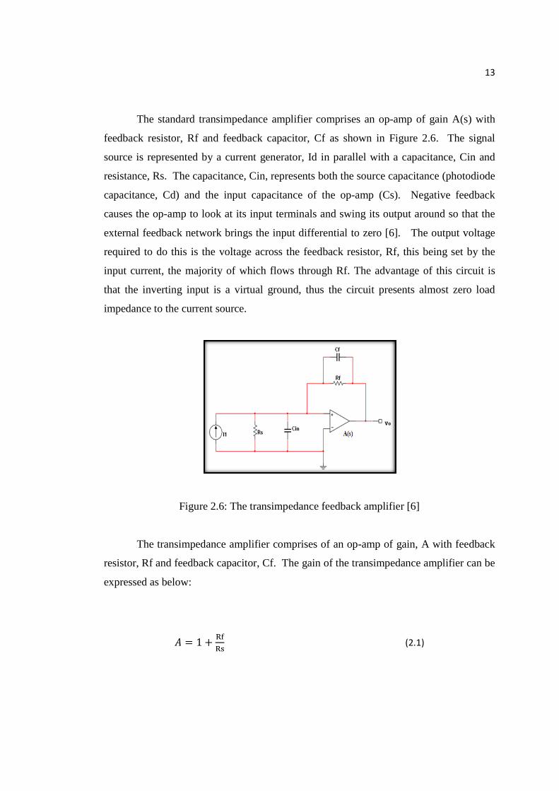
The standard transimpedance amplifier comprises an op-amp of gain A(s) with
feedback resistor, Rf and feedback capacitor, Cf as shown in Figure 2.6. The signal
source is represented by a current generator, Id in parallel with a capacitance, Cin and
resistance, Rs. The capacitance, Cin, represents both the source capacitance (photodiode
capacitance, Cd) and the input capacitance of the op-amp (Cs). Negative feedback
causes the op-amp to look at its input terminals and swing its output around so that the
external feedback network brings the input differential to zero [6]. The output voltage
required to do this is the voltage across the feedback resistor, Rf, this being set by the
input current, the majority of which flows through Rf. The advantage of this circuit is
that the inverting input is a virtual ground, thus the circuit presents almost zero load
impedance to the current source.
Figure 2.6: The transimpedance feedback amplifier [6]
The transimpedance amplifier comprises of an op-amp of gain, A with feedback
resistor, Rf and feedback capacitor, Cf. The gain of the transimpedance amplifier can be
expressed as below:
� � 1 ���
�� (2.1)

14
2.2 Gain Bandwidth Product
One character of amplifier is that the product of the voltage gain and the bandwidth is
always constant when the roll- off is -20dB/decade. This characteristic is called the gain-
bandwidth product. Let’s assume that the lower critical frequency of a particular
amplifier is much less than upper critical frequency, fcl << fcu.
The bandwidth can then be approximated as BW � �� � ��� ≅ ��
The simplified Bode plot for this condition is shown in Figure 2.7 below.Notice
that fcl is neglected because it is so much smaller than fcu, and the bandwidth
approximately equal fcu. Beginning at fcu, the gain rolls off until unity gain (0 dB) is
reached. The frequency at which amplifier’s gain is 1 is called the unity gain frequency,
fT. The significant of fT is that it always equal the product of the midrange voltage gain
times the bandwidth and is constant for given transistor [7].
�� � Av�mid�BW (2.2)
Figure 2.7: Simplified response curve where fc1 is negligible(assume to be zero) compare
to fcu [7]

15
2.3 Transistor Amplifier Analysis and Small Signal Model
Small signal model is using to determine the transistor amplifier characteristic such as
Gain. The ability of small-signal BJT circuit models makes the analysis of transistor
amplifier circuits a systematic process. The process consists of the following steps [8]:
1. Determine the dc operating point of the BJT and in particular the dc collector
current Ic.
2. Calculate the values of the small-signal model parameters : g� ���
����
�
and !" ≅ ���# ≅$�
3. Eliminate the dc source by replacing each dc voltage source with a short circuit
and each dc current source with an open circuit.
4. Replace the BJT with one of its small-signal equivalent circuit models. Although
any one of the models can be used, one might be more convenient than the others
for the particular circuit being analyzed.
5. Analyzed the resulting circuit to determine the required quantities (e.g., voltage
gain, input resistance).
There are two type of basic small-signal model which is ‘Hybrid-π Model’ and ‘T
Model’.

16
2.3.1 Hybrid-π Model
Figure 2.8: The amplifier circuit with dc source VBE and VCC eliminated (short
circuit) [8].
An equivalent circuit model for BJT is shown in Figure 2.8. This model represents the
BJT as a voltage-controlled current source and explicitly includes the input resistance
looking into the base, rπ. The model obviously yields %� = g�&'" and () = *+,-. . Not so
obvious, however, is the fact that the model also yields the correct expression for ie. This
can be shown as follow;
Emitter node:
%" = &'"!/+ g�0'" =
&'"!/(1 + g�!/)
%" = *+,-. (1 + 1) =*+,2.345
(2.3)

17
A slight different equivalent circuit model can be obtained by expressing the
current of the controlled source (g�&'") in terms of the base current ib as follows:
g�&'" = g�(%'!/) = (g�!/)%' = 1%' (2.4)
This results in the alternative equivalent circuit model show in Figure 2.9(b).
Here the transistor is represented as current-controlled current source, with the control
current being ib. The two model of Figure 2.9 are simplified version of what is known as
the Hybrid-π Model. This is most widely used model for BJT [8].
Figure 2.9: (a) BJT as a voltage-controlled current source ( a transconductance
amplifier) (b) BJT as a current-controlled current source (a current amplifier)[8].
It is important to note that the small-signal equivalent circuits of Figure 9 model
the operation of BJT at a given bias point. This should be obvious from the fact that the
model parameters g� and !/ depend on the value of the dc bias current ic. Finally,
although the models have been developed for an npn transistor, they apply equally well
to pnp transistor with no change of polarities.
The output resistance ro should be added if the circuit amplifier is considering the
early effect. The early effect causes the collector current to depend not only on VBE but
also on VCE. The dependence on VCE can modeled by assigning a finite output
resistance to the controlled current-source in the ‘Hybrid-π Model’ as shown in Figure

18
2.10 .Its value is given by !6 ≅ 07/%� , where VA is the early voltage and ic is the
collector dc bias current.
The output voltage becomes;
06 = −g�&'"(9�//!:) (2.5)
Figure 2.10: Hybrid-π Model with the resistance r0 included [8].
2.3.2 T Model
Although the hybrid-π model can be used to carry out small-signal analysis of all
transistor circuit, there are situations in which an alternative model, shown in Figure
2.11. This model, called the T model. The T model of Figure 2.11 (a) represents the
BJTas a voltage-controlled current source with the control voltage being &'". However,
the resistance between base and emitter, looking into the emitter, is explicitly shown.
From the Figure. 2.11(a) we see clearly that the model yields the correct expressions for
ic and ie. For ib we note that at the base node we have;
%' = &'"!"+ g�&'" =
&'"!"(1 − ;�!")
%' = *+,-, (1 + <) =*+,-,=1 − �
�>$? =*+,
(�>$)-,= *+,-. (2.6)

19
(a) (b)
Figure 2.11: T model of BJT (a) BJT as a voltage-controlled current source (b) BJT as a
current-controlled current source[8].
If in the model Figure 2.11 (a) the current of the controlled source is expressed in
terms of emitter current as follows:
g�&'" � g��%"!"� � �g�!"�%" � <%" (2.7)
obtained the alternative T-model shown in Figure 2.11(b). Here the BJT is represented
as current-controlled current source but with the control signal being ie [8].
The Hybrid-Π and the T circuit models are equivalent, because they both will
result in the same correct answer.
20
2.4 Previous Research Review
This section present the past research based on bandwidth enhancement. Previous design
method and technique have been developed by designer had been compared as a guided
to design the front-end receiver and in order to achieved the project objective.
2.4.1 First Review
Author: Reza Samadi and Aydın Ilker Karsilayan.
Project Title: Uniform Design of Multi-Peak Bandwidth Enhancement Technique
for Multistage Amplifiers
Summary:
This paper introduces a new technique for designing uniform
multistage amplifiers (MAs) for high-frequency applications is
introduced. The proposed method uses the multi-peak bandwidth
enhancement technique while it employs identical, simple and
inductorless stages. The intrinsic capacitances within transistors are
exploited by the active negative feedbacks to expand the bandwidth.
While all stages of the proposed MA topology are identical, the gain-
bandwidth product can be extended several times. Using the proposed
topology, a six-stage amplifier in TSMC 0.35- m CMOS process was
designed. Measurement results show that the gain can be varied
between 16 and 44 dB within 0.7–3.2-GHz bandwidth with less than
5.2-nV Hz noise. Die area of the amplifier is 175 m 300 m.
Performance of these systems is usually affected by
bandwidth and gain limitation of amplifiers. High voltage gain from
dc to several gigahertz frequencies is acquired by cascading several
gain stages in the form of multistage amplifiers (MAs).
A new topology entitled the chained MA (CMA), which uses
the peaking technique to expand the bandwidth while the topology

21
can be implemented uniformly. Due to active feedback, amplifier
sections can be designed with low quality factors and with no
inductors. In addition, CMA exploits the intrinsic capacitance within
the transistors to push output pole of each stage to a higher frequency.
The topology of CMA offers several advantages such as improved
performance and gain-bandwidth product that make the proposed
structure suitable for optical communications.
Figure 2.12: Three-stage conventional MA
A typical MA can be designed by cascading simple gain
stages. Figure 2.12 above illustrates a three-stage MA consisting of
three forward amplifiers with gains of g1, g2 and g3 where the overall
gain is g1g2g3.
Topology of the proposed amplifier is illustrated in Figure
2.13. The overall structure consists of identical forward amplifiers
with identical active feedbacks . The transfer function of the uniform
-stage CMA can be obtained as shown as Figure 2.14 where L(s) =
g(s)f(s) is the loop gain [9].
Figure 2.13: Topology of the proposed MA[9].
Figure 2.14: Topology of the uniform 2-stage CMA[9].

22
2.4.2 Second Review
Author: Feng-Tso Chien and Yi-Jen Chan
Project Title: Bandwidth Enhancement of Transimpedance Amplifier by a
Capacitive-Peaking Design
Summary:
From the research paper the author is proposing a capacitive-
peaking (C-peaking) technique, instead of inductive peaking, to
increase the bandwidth of a transimpedance amplifier. The reports of
a peaking technique using capacitors are very few. Although some
different types of the capacitance peaking have been proposed
previously. An optoelectronic receiver, which usually consists of a
photodetector and a transimpedance amplifier, is used to convert the
optical signals into electrical signals in the front end of optical fiber
communication. Based on that fact, we can design a larger bandwidth
of a transimpedance amplifier. From this paper, they only discuss the
idea of capacitor peaking technique and also derive an analytical
method to predict the amplifier performance.
A TZ amplifier can be represented as a shunt shunt feedback
amplifier, and the transfer function of this circuit is given by:
Where A(s) is the open-loop transfer function of the TZ amplifier and
β(s) is the feedback transfer function or simply a feedback factor. Rf
is the effective feedback resistance and Cf is the parasitic capacitance
associated with Rf [9]. Figure. 2.15(a) shows the schematic circuit of
this C-peaking TZ amplifier. In order to analyze the peaking effect
resulting from this peaking capacitor first, they derive the open-loop
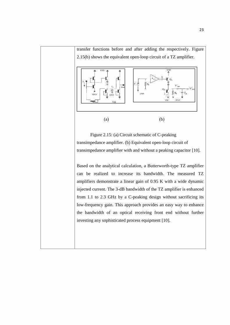
23
transfer functions before and after adding the respectively. Figure
2.15(b) shows the equivalent open-loop circuit of a TZ amplifier.
(a) (b)
Figure 2.15: (a) Circuit schematic of C-peaking
transimpedance amplifier. (b) Equivalent open-loop circuit of
transimpedance amplifier with and without a peaking capacitor [10].
Based on the analytical calculation, a Butterworth-type TZ amplifier
can be realized to increase its bandwidth. The measured TZ
amplifiers demonstrate a linear gain of 0.95 K with a wide dynamic
injected current. The 3-dB bandwidth of the TZ amplifier is enhanced
from 1.1 to 2.3 GHz by a C-peaking design without sacrificing its
low-frequency gain. This approach provides an easy way to enhance
the bandwidth of an optical receiving front end without further
investing any sophisticated process equipment [10].
24
2.4.3 Third Review
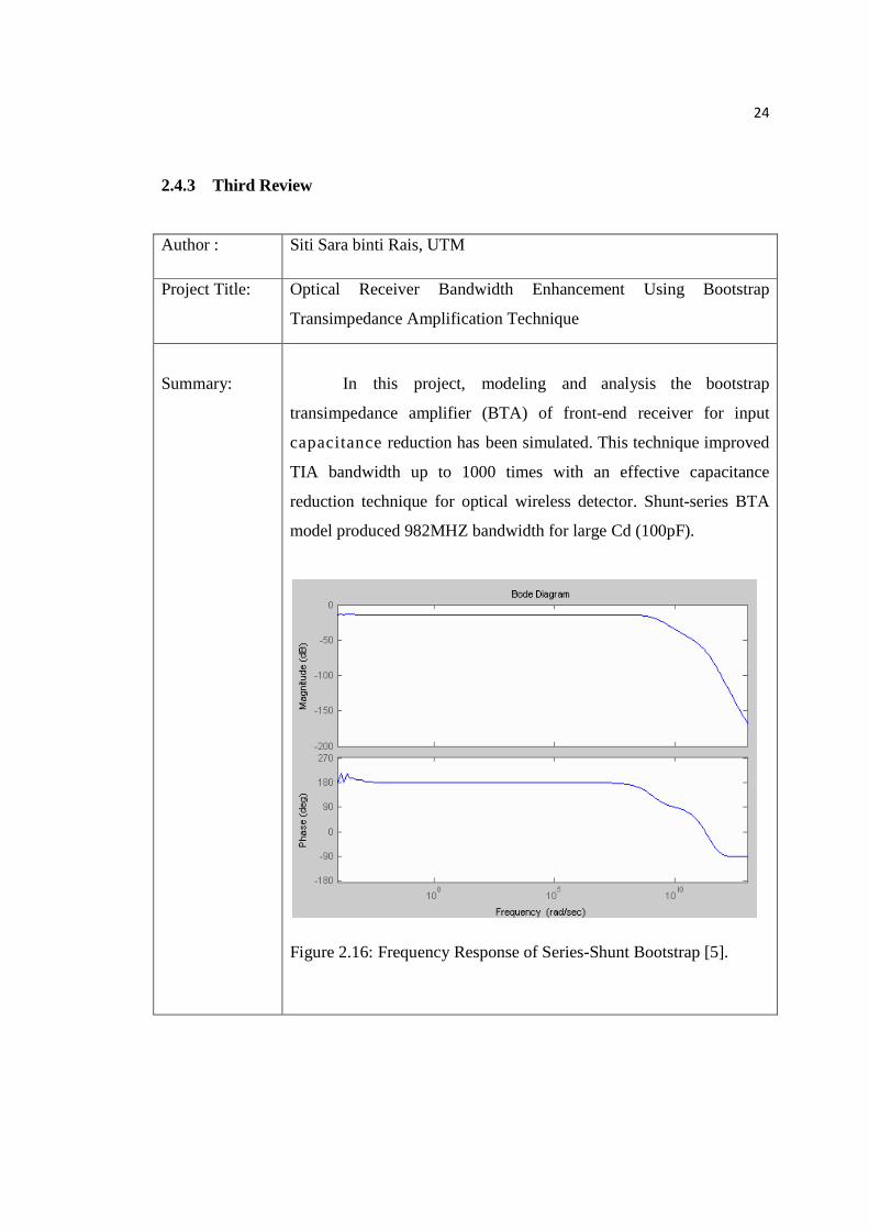
Author : Siti Sara binti Rais, UTM
Project Title: Optical Receiver Bandwidth Enhancement Using Bootstrap
Transimpedance Amplification Technique
Summary:
In this project, modeling and analysis the bootstrap
transimpedance amplifier (BTA) of front-end receiver for input
capacitance reduction has been simulated. This technique improved
TIA bandwidth up to 1000 times with an effective capacitance
reduction technique for optical wireless detector. Shunt-series BTA
model produced 982MHZ bandwidth for large Cd (100pF).
Figure 2.16: Frequency Response of Series-Shunt Bootstrap [5].

52
REFERENCES
1. Ramli,A. Idrus, S. M.Supa'at,A.S.M & Rais,S.S (2008). Bandwidth
Enhancement Technique using Series-Shunt Bootstrapping for Front-End Optical
Wireless Receiver. IEEE. pp.52-56
2. Iniguez, R. R.Idrus,S. M. & Sun,Z.(2007).Optical Wireless Communications: IR
for Wireless Connectivity. Auerbach Publications. Taylor and Francis Books
Inc, New York.
3. Keiser, G. (2000).Optical Fiber Communications. 3nd.USA: MCGraw-Hill.
4. Alexander S, B. (1997) .Optical Communication Receiver Design. Bellingham,
Washington: SPIE The International Society for Optical Engineering.
5. Rais,S.S. (2006) Optical Receiver Bandwidth Enhancement Using Bootstrap
Transimpedance Amplification Technique. Universiti Teknologi Malaysia:
Master.Thesis
6. Steve Hranilovic (2004).Wireless Optical Communication Systems.Assistant
Professor, Department of Electrical and Computer Engineering, McMaster
University, Hamilton, Ontario, Canada, Springer Science+Business Media, Inc.
7. Flyod,T.L.( 2002).Electronic Devices.6nd.USA:PrenticeHall.
53
8. Sedra,A.S & Smith,K.C.(1998). Microelectronic Circuits.4nd.New York :Oxford
University Press.
9. Samadi,R. & Karsilayan, A.R.(2007).Uniform Design of Multi-Peak Bandwidth
Enhancement Technique for Mutlistage Amplifiers. Transaction On Circuits And
Systems,54(7),pp1489-1499.
10. Chien,F.T & Chan.(1999). Bandwidth Enhancement of Transimpedance
Amplifier by a Capacitive-Peaking Design.Solid-State Circuits,34(8),pp 1167-
1170.
11. Hoyle, C. and Peyton, A.(1999). Shunt Bootstrapping Technique To
Improve Bandwidth Of Transimpedance Amplifiers. Electronics Letters. 35(5),
pp 369 – 370
12. Abdullah,M.F.L. & Green,R.J.(2011).Receiver Front-End Bandwidth
Enhancement Design.Telecomunication,Electronic and Computer
Engineering.3(1,pp.69-78
13 Boylestad,R & Nashelsky,L.(1996). Electronic Devices And Circuit Theory.
6nd.New Jersey :Prentice Hall International.
14 John, M.Senior,L.(2009). Optical fiber Communications Prinsiples and
Prectice. 3nd. England : Person Education.
15 Palais,J.C.(2005). Fiber Optic Communicatios. 5nd. New Jersey : Person
Education.
15 Flyod,T.L.(2003). Priciples of Electric Circuit. 7nd. New Jersey : Person
Education.
54
16 Palais,J.C.(2005). Fiber Optic Communicatios. 5nd. New Jersey : Person
Education.
17 Ahmad,M.F. (2010). Optical Wireless Receiver Amplifier Using Hybrid
Bandwidth Enhancement. Universiti Tun Hussein Onn Malaysia: Degree.Thesis.
18 Mahat,M. (2009). Automatic Bandwidth Control Receiver Using Bootstrap
Transimpedance Amplifier Technique. Universiti Tun Hussein Onn Malaysia:
Degree.Thesis.
19. Ramli,A. Idrus, S. M.Supa'at,A.S.M & Rais,S.S (2008). Modeling of a Series
Bootstrapping Pre-amplifier Circuit for Free Space Optics. Telecommunication
Technologies and IEEE 2008 2nd Malaysia Conference on Photonics. pp.37-41
20. Idrus,S.M.Ngajikin,N.Malik,N.N.N.A and Aziz,S.I.A (2006). Performance
Analysisof Bootstrap Tranimpidance Amplifier For Large Windows Optical
Wireless Receiver. International RF and Microwave ConferenceProceedings.
pp.416-420