Embed Size (px)
DESCRIPTION
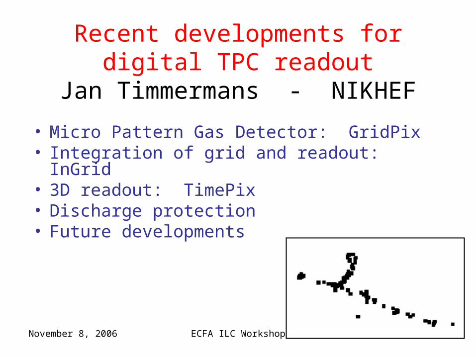
Recent developments for digital TPC readout Jan Timmermans - NIKHEF. Micro Pattern Gas Detector: GridPix Integration of grid and readout: InGrid 3D readout: TimePix Discharge protection Future developments. Goals. Gas multiplication GEM or Micromegas foil(s) - PowerPoint PPT Presentation
Citation preview
November 8, 2006 ECFA ILC Workshop 1
Recent developments for digital TPC readout
Jan Timmermans - NIKHEF
• Micro Pattern Gas Detector: GridPix• Integration of grid and readout: InGrid• 3D readout: TimePix • Discharge protection• Future developments
November 8, 2006 ECFA ILC Workshop 2
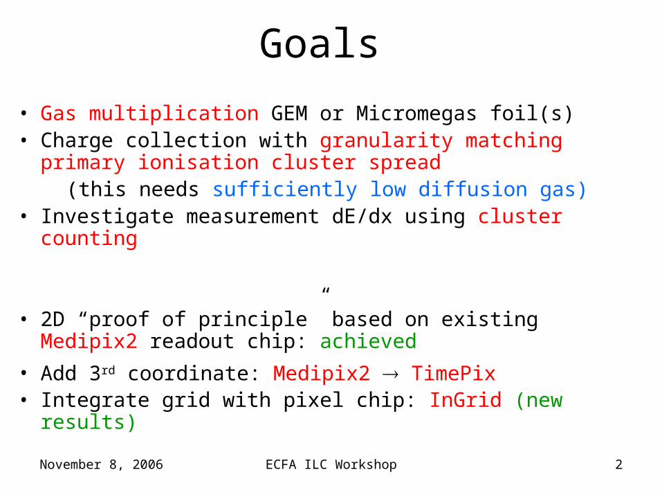
Goals
• Gas multiplication GEM or Micromegas foil(s)• Charge collection with granularity matching primary
ionisation cluster spread (this needs sufficiently low diffusion gas)• Investigate measurement dE/dx using cluster counting
• 2D “proof of principle” based on existing Medipix2 readout chip: achieved
• Add 3rd coordinate: Medipix2 TimePix • Integrate grid with pixel chip: InGrid (new results)

November 8, 2006 3
Micro Patterned Gaseous Detectors
GEM
Micromegas
• High field created by Gas Gain Grids
• Most popular: GEM & Micromegas
Use ‘naked’ CMOS pixel readout chip as anode
4
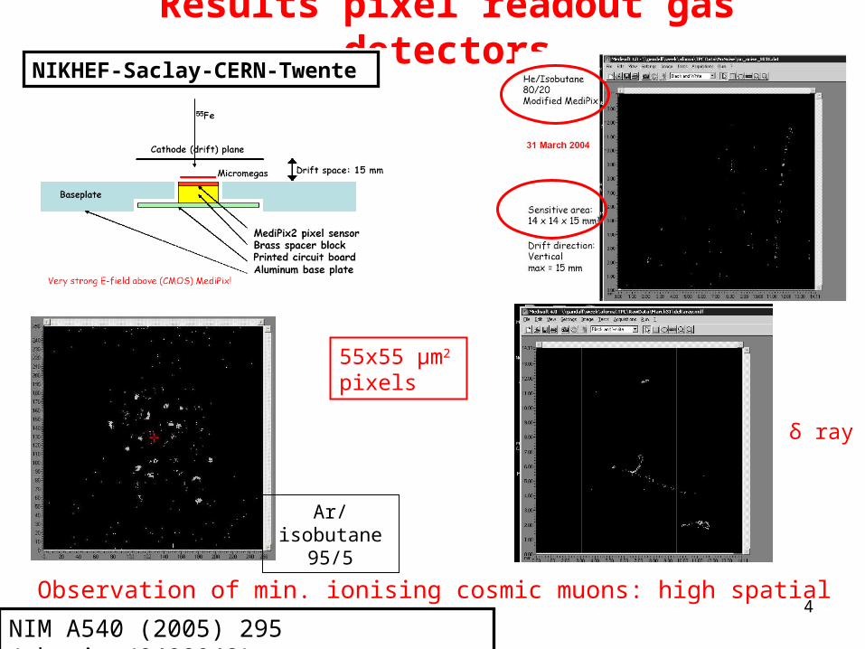
Results pixel readout gas detectors
Observation of min. ionising cosmic muons: high spatial resolution + individual cluster counting !
δ ray
NIKHEF-Saclay-CERN-Twente
NIM A540 (2005) 295 (physics/0409048)
55x55 μm2 pixels
Ar/isobutane 95/5

November 8, 2006 ECFA ILC Workshop 5
(from Freiburg GEM+Medipix setup - Andreas Bamberger)
Difference between Micromegas and GEM setup understood (simulation Michael Hauschild/CERN)
~ 50 μm resolution
Triple GEM
Total gain ~60k
(β source)
November 8, 2006 ECFA ILC Workshop 6
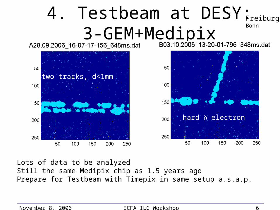
4. Testbeam at DESY: 3-GEM+Medipix
FreiburgBonn
Lots of data to be analyzedStill the same Medipix chip as 1.5 years agoPrepare for Testbeam with Timepix in same setup a.s.a.p.
two tracks, d<1mm
hard electron
November 8, 2006November 8, 2006 77
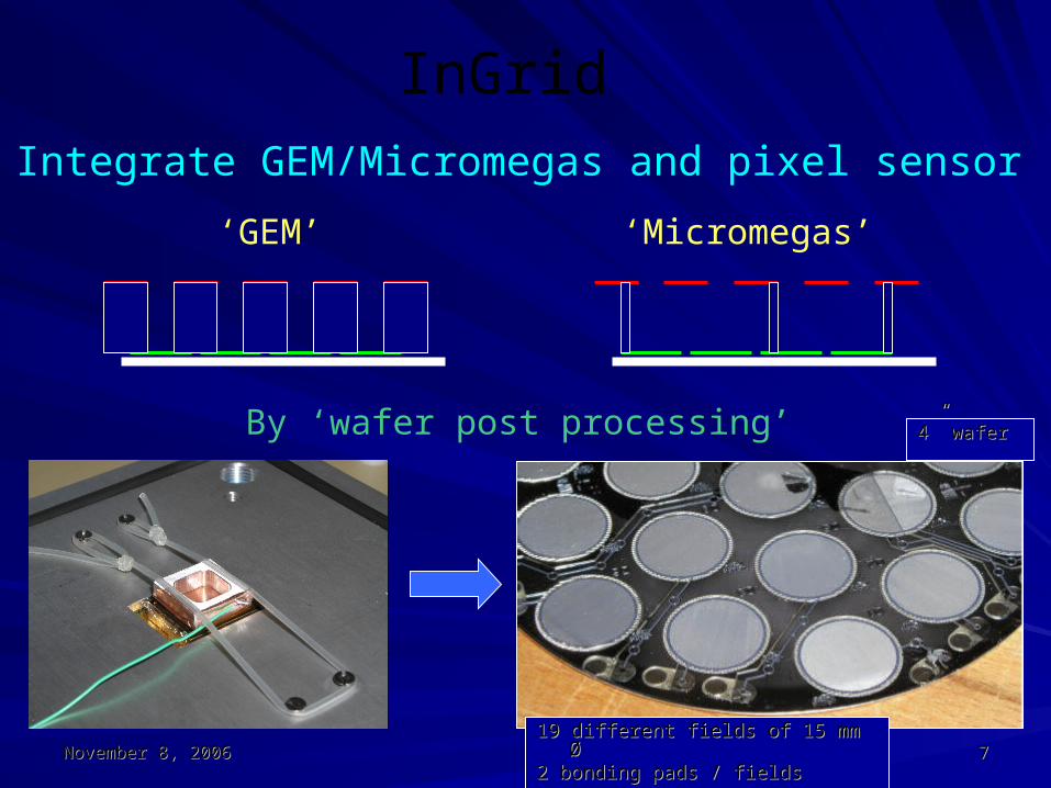
Integrate GEM/Micromegas and pixel sensor
‘GEM’ ‘Micromegas’
By ‘wafer post processing’
InGrid
19 different fields of 15 mm Ø19 different fields of 15 mm Ø2 bonding pads / fields2 bonding pads / fields
4” wafer4” wafer

November 8, 2006 ECFA ILC Workshop 8
NIKHEF/Twente: InGrid (Integrated Grid)
Deposit anode Deposit SU-8
UV exposure Deposit metal
Pattern metal Develop resist
November 8, 2006 ECFA ILC Workshop 9
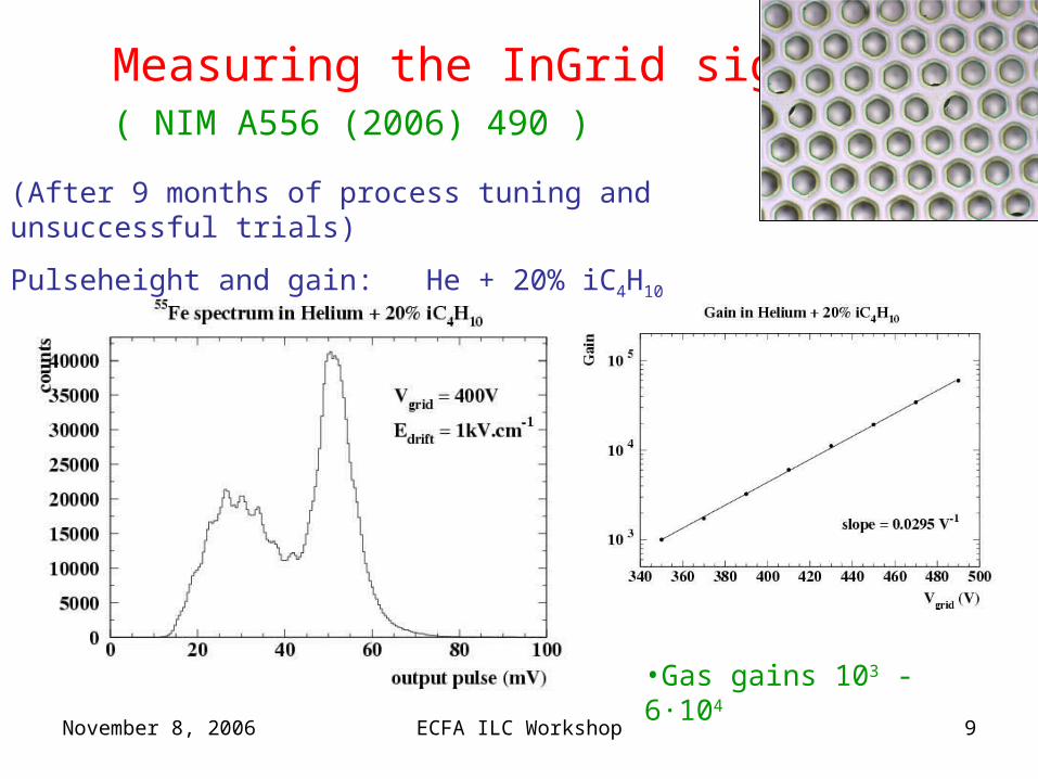
Measuring the InGrid signals ( NIM A556 (2006) 490 )
(After 9 months of process tuning and unsuccessful trials)
Pulseheight and gain: He + 20% iC4H10
•Gas gains 103 - 6∙104
November 8, 2006 ECFA ILC Workshop 10
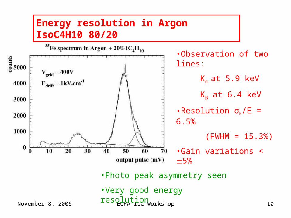
Energy resolution in Argon IsoC4H10 80/20
•Observation of two lines:
Kα at 5.9 keV
Kβ at 6.4 keV
•Resolution σE/E = 6.5%
(FWHM = 15.3%)
•Gain variations < 5%
•Photo peak asymmetry seen
•Very good energy resolution

November 8, 2006 ECFA ILC Workshop 11
Any field structure feasible

November 8, 2006 ECFA ILC Workshop 12
Gain for different gap sizesMaximum predicted in gain vs gap curve
Gap (mm)
Y. Giomataris/N.I.M. A419 (1998) 239-250
0.001 0.01 0.1 11
10
1000
100
10000
Ga
in
V=400Volts
V=350Volts
V=300Volts
deM d gap thickness
p pressure
A,B depend on gasmixture

November 8, 2006 ECFA ILC Workshop 13
Gain for different gap sizes• But now we can make measurements
Grid voltage
Ga
in
300 380 460 540Gap thickness (μm)
35 45 6555 75102
103
104
105
400V450V500V
75um35um55um40um

November 8, 2006 ECFA ILC Workshop 14
Homogeneity
• Gain measurements scanning the surface of the detector• Homogeneity given by grid quality
2.6 % RMS 1.6 % RMSx
yyx
Gain Gain
November 8, 2006 ECFA ILC Workshop 15
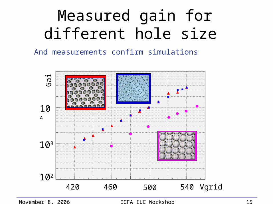
Measured gain for different hole size
Ga
in
Vgrid460 500 540420
103
104
102
And measurements confirm simulations

November 8, 2006 ECFA ILC Workshop 16
Energy resolution• Resolution depends on
– Primary,attachment,T,P– Collection efficiency (field ratio)– Gain homogeneity & transverse diffusion
103 10410
20
30
40
60
Re
solu
tion
(FW
HM
%)
Gain

November 8, 2006 ECFA ILC Workshop 17
Resolution as function of gap
• Why a parabolic behavior ?
Vgrid
Re
solu
tion
(FW
HM
%)
20
30
40
50 35um55um75um
380 420 460 500
Gain
Energy resolution
F. Jeanneau et al. NIM A 461 (2001) 84–87

18
TimePix1(EUDET: Freiburg, Saclay, CERN, NIKHEF)
•Distribute clock to full 256x256 pixel matrix (50-100-160MHz)
•Enable counting by first hit after ‘shutter’ opens, until ‘shutter’ closes (common stop); also time-over-threshold possible
•Dynamic range 214 x 10 ns = 160 μs
•(for the time being) no zero-suppress
to remain fully compatible with Medipix2
•Shaping time ~200 ns
•Keep same chip-size, pixel-size, readout protocol
•1st full reticle submit done July 2006; IT WORKS! Now preparing/doing tests in gas detectors.
11 22 44
55
66
55μm
55μm

November 8, 2006 ECFA ILC Workshop 19
Sparking• Chip faces 80kV/cm with no protection (unlike
the GEM setup; 1.5 yr using same chip)• Degradation of the field, or total destruction
of grid but also CMOS chip
10μm

November 8, 2006 ECFA ILC Workshop 20
CMOS Chip protection against - discharges- sparks- HV breakdowns- too large signals
Empirical method:Try RPC technology
Amorph Si (segmented)
Silicon Protection: SiProt

November 8, 2006 ECFA ILC Workshop 21
- RPC principle: reduction of local E-field- Avalanche charge: electrostatic induction towards input pad- Specific resistance: - high enough to ‘block’ avalanche charge
- low enough to flow signal current- layer thickness 4 μm, Rvol = 0.2 GΩ/cm
TechnologyA-Si deposit possible in general; avoid wafers get too hot
Univ. of Neuchatel/IMT/P. Jarron (CERN) uses this for integrated X-ray sensor/convertor on MediPix 2
--- -
Test: put Thorium in gas: Radon α-decays: - large (proportional) signals
- Discharges: like short circuits
plasmaA-Si
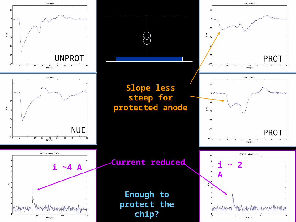
UNPROT PROT
PROT
PROT
Enough to protect the chip?NUE
NUE
Slope less steep for protected anode
Current reducedi ~4 A i ~ 2 A
23
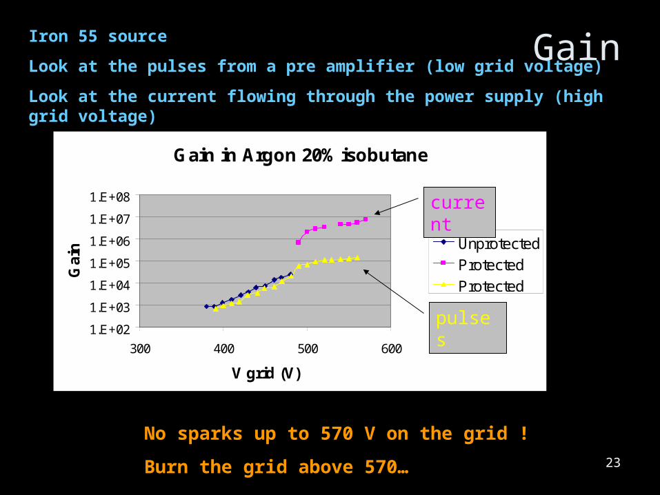
Gain in Argon 20% isobutane
1.E+02
1.E+03
1.E+04
1.E+05
1.E+06
1.E+07
1.E+08
300 400 500 600
V grid (V)
Gai
n Unprotected
Protected
Protected
Iron 55 source
Look at the pulses from a pre amplifier (low grid voltage)
Look at the current flowing through the power supply (high grid voltage)
No sparks up to 570 V on the grid !
Burn the grid above 570…
Gain
current
pulses
November 8, 2006 ECFA ILC Workshop 24
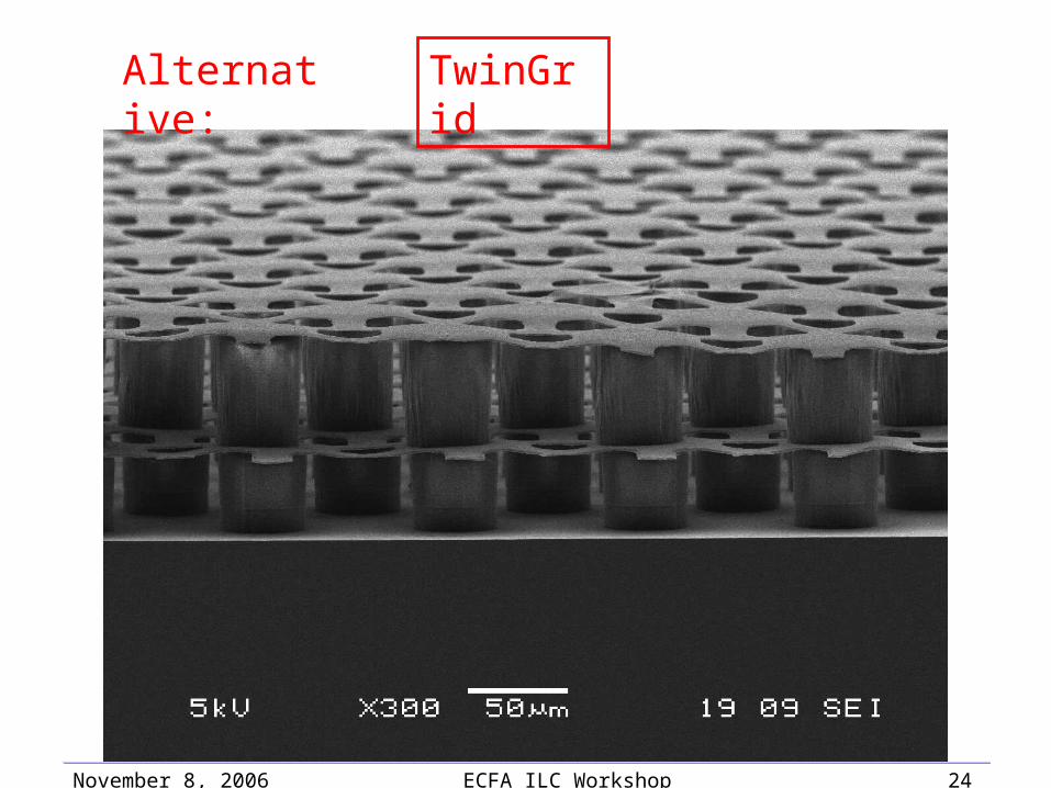
TwinGridAlternative:
November 8, 2006 ECFA ILC Workshop 25
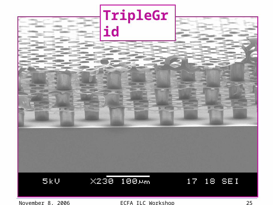
TripleGrid
November 8, 2006 ECFA ILC Workshop 26
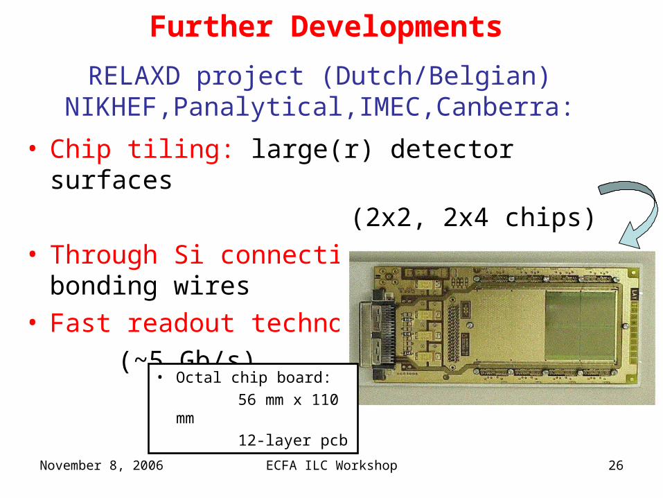
Further Developments
• Chip tiling: large(r) detector surfaces
(2x2, 2x4 chips)• Through Si connectivity: avoiding bonding wires• Fast readout technology
(~5 Gb/s)
RELAXD project (Dutch/Belgian) NIKHEF,Panalytical,IMEC,Canberra:
• Octal chip board:
56 mm x 110 mm
12-layer pcb

November 8, 2006November 8, 2006 ECFA ILC WorkshopECFA ILC Workshop 2727
GridPix: the electronic bubble chamber
NIKHEF Harry van der GraafJan TimmermansJan VisschersMaximilien ChefdevilleMartin FransenVladimir Gromov
Saclay CEA DAPNIA Paul Colas, David AttiééDan Burke,Yannis Giomataris
Arnoud Giganon, Marc Riallot
Univ. Twente/Mesa+ Jurriaan SchmitzCora Salm
Victor Blanco CarballoSander Smits
CERN Michael Campbell,Erik Heine Xavi Llopart
Thanks to:Wim GotinkJoop Rovenkamp