Embed Size (px)
Citation preview
- 161 -
Current Optics and Photonics Vol. 4, No. 3, June 2020, pp. 161-173
ISSN: 2508-7266(Print) / ISSN: 2508-7274(Online) DOI: https://doi.org/10.3807/COPP.2020.4.3.161Invited Paper
I. INTRODUCTION
Colloidal quantum dots (QDs), which are semiconductor
nanoparticles, have attracted considerable attention because
of their advantageous features, such as tunable emission
spectra (from ultraviolet to infrared), remarkable photo-
luminescence (PL), and narrow full-width at half-maximum
emission bandwidth [1-8]. QDs have been regarded as a
key material that can enable next-generation displays, given
their advantages of high PL quantum yields (QYs) and
cost-effective, solution-based processability [9-15]. Recently,
a QD-based color-enhancement film was commercialized
successfully in the display market, establishing the superiority
of QDs in display applications. Intensive studies are now
being conducted to realize the next technology frontier: the
replacement of present-day emissive display technologies
with QD light-emitting diodes (QLEDs).
The first QD-based electroluminescent device was demon-
strated by Colvin et al. in 1994 [16]. The luminescence
properties of QLEDs improved dramatically over the
subsequent two decades with the development of high
quality QDs, establishment of the standard p-i-n multilayered
QLED structure [1, 2, 17-20], improved charge-injection
and transport characteristics [2, 20-25], and increased light-
extraction efficiency [26-28]. As a result of intensive
studies, the luminescence efficiency of QLEDs has improved
considerably (by over three orders of magnitude, from
0.01% to >20%) to approach the theoretical maximum [5,
19, 29-32]. Simultaneously, the brightness of QLEDs has
increased significantly from the initially demonstrated value
Recent Progress in High-Luminance Quantum Dot Light-Emitting Diodes
Seunghyun Rhee1, Kyunghwan Kim1, Jeongkyun Roh2*, and Jeonghun Kwak1
**
1Department of Electrical and Computer Engineering, Inter-university Semiconductor Research Center (ISRC),
Seoul National University, Seoul 08826, Korea2Department of Electrical Engineering, Pusan National University, Busan 46241, Korea
(Received March 11, 2020 : revised March 26, 2020 : accepted March 26, 2020)
Colloidal quantum dots (QDs) have gained tremendous attention as a key material for highly advanced
display technologies. The performance of QD light-emitting diodes (QLEDs) has improved significantly
over the past two decades, owing to notable progress in both material development and device engineering.
The brightness of QLEDs has improved by more than three orders of magnitude from that of early-stage
devices, and has attained a value in the range of traditional inorganic LEDs. The emergence of
high-luminance (HL) QLEDs has induced fresh demands to incorporate the unique features of QDs into
a wide range of display applications, beyond indoor and mobile displays. Therefore it is necessary to assess
the present status and prospects of HL-QLEDs, to expand the application domain of QD-based light sources.
As part of this study, we review recent advances in HL-QLEDs. In particular, based on reports of brightness
exceeding 105 cd/m2, we have summarized the major approaches toward achieving high brightness in
QLEDs, in terms of material development and device engineering. Furthermore, we briefly introduce the
recent progress achieved toward QD laser diodes, being the next step in the development of HL-QLEDs.
This review provides general guidelines for achieving HL-QLEDs, and reveals the high potential of QDs
as a universal material solution that can enable realization of a wide range of display applications.
Keywords : Quantum dots, High luminance, QLED, QD laser diode
OCIS codes : (130.0250) Optoelectronics; (230.3670) Light-emitting diodes; (160.4236) Nanomaterials
*Corresponding author: [email protected], ORCID 0000-0002-0674-572X
**Corresponding author: [email protected], ORCID 0000-0002-4037-8687
Color versions of one or more of the figures in this paper are available online.This is an Open Access article distributed under the terms of the Creative Commons Attribution Non-Commercial License (http://creativecommons.org/licenses/by-nc/4.0/) which permits unrestricted non-commercial use, distribution, and reproduction in any medium, provided the original work is properly cited.
Copyright 2020 Current Optics and Photonics
Current Optics and Photonics, Vol. 4, No. 3, June 2020162
of 102 cd/m2 to a recently reported value exceeding 106
cd/m2 [33]. As the brightness of QLEDs has improved
continuously, to finally equal those in the brightness range
of traditional inorganic LEDs (>106 cd/m2), fresh demands
to exploit the remarkable features of QLEDs in a wider
range of display applications beyond indoor and mobile
displays have arisen.
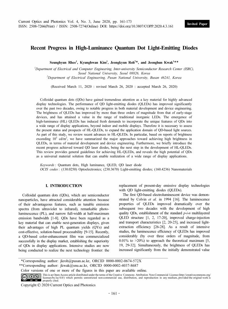
Figure 1(a) shows a broad range of display applications,
with respect to required brightness. According to their
purposes and operating conditions, displays require different
levels of maximum brightness, the so-called white level, to
guarantee visibility. For example, indoor and mobile displays
require a brightness of 102~103 cd/m2, whereas public
outdoor displays require a higher brightness (>103 cd/m2).
When the displays are used in harsh environments such as
direct sunlight, brightness exceeding 104 cd/m2 is required
to ensure high visibility. Furthermore, when an optical
projection-type display is used to provide spatial visuali-
zation or magnification, a significantly higher brightness
(>105 cd/m2) is necessary to overcome the low transmittance
of optical projection systems, which may be less than 1%.
In this domain, LEDs with high luminance can be used
in low-power projection systems (e.g. AR/VR displays).
However, a laser diode is a better option for high-power
applications such as head-up or cinema displays.
In principle, QDs are expected to be a universal material
solution that can cover the entire range of applications
with regard to brightness, shown in Fig. 1(a). In the early
stages of development, QLEDs were able to cover the
low-brightness application regime; at present, they are
capable of expanding their applicability to the higher-
brightness regime. QD-based light sources covering the
brightness regime >105 cd/m2 are termed high-luminance
QLEDs (HL-QLEDs), to distinguish them from the QLEDs
for traditional applications. Furthermore, the remaining
region can be covered by developing the final type of
QD-based light source: QD laser diodes. This growing
adoption of QD-based light sources will provide fresh
opportunities to traditional display applications by delivering
the unique features of QDs, such as flexibility [14, 28,
34], inexpensive solution processability [13, 31, 35], and
conveniently tunable emission color [1-3].
Here, as an aid to boost this growth, we review the
recent progress and remaining challenges of HL-QLEDs.
We briefly introduce the fundamental operating principles
of QLEDs, and then highlight the key factors for achieving
HL-QLEDs in terms of two important aspects: material
development and device engineering. We summarize the
current status of HL-QLEDs with a few important milestones.
This is followed by a description of remaining challenges.
A review of the key factors impelling HL-QLED technology
will guide us to the recent development toward a QD laser
diode, which is a longstanding goal in this research field.
We cover the most recent research advances in the
development of QD laser diodes, and briefly discuss the
future prospects. This review introduces the great potential
of QDs as a universal material solution to enable a wide
range of display applications, and to aid in expanding the
application domain of QD-based light sources.
FIG. 1. (a) Display applications of QD-based light sources, with respect to required brightness. (b) Schematic of a standard QLED
structure, and its energy-band diagram.
Recent Progress in High-Luminance Quantum Dot Light-Emitting Diodes - Seunghyun Rhee et al. 163
II. METHODS FOR EMPLOYING HL-QLEDS
Intensive studies to improve the performance of QLEDs
have resulted in the establishment of a standard device
structure based on p-i-n multilayers [4, 5, 7, 8, 28, 33,
36]. This state-of-the-art QLED structure comprises a metal
anode, hole-transport layer (HTL), QD emissive layer,
electron-transport layer (ETL), and an ITO cathode, as
shown in Fig. 1(b). The HTL and ETL transfer charge
carriers from each electrode to the QDs. The injected
carriers (electrons and holes) recombine within the QDs,
which generate photons having energy corresponding to
that of the QD band gap. Therefore, as can be derived
from the operating principle of QLEDs, HL-QLEDs can be
realized by (ⅰ) injecting and transporting charges efficiently,
(ⅱ) using QDs with high luminescence efficiency (that is PL
QY), and (ⅲ) improving the light-extraction property. An
additional important factor is the carrier-rich environment of
HL-QLEDs due to high-current excitation, which produces
multiexciton species in QDs [9, 33, 34]. Therefore, the
suppression of multiexciton-related nonradiative recombi-
nation, known as Auger recombination, is significant for
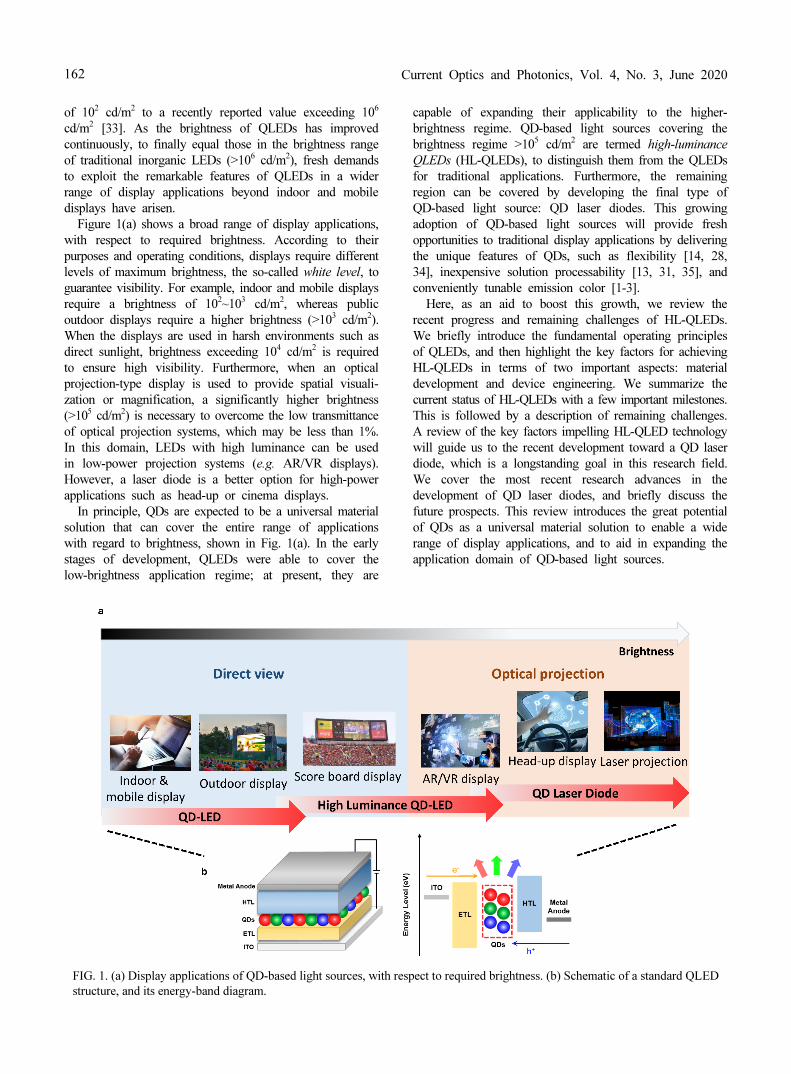
achieving HL-QLEDs. Intensive studies have been performed
to address those key issues. As a result, the brightness of
QLEDs has improved continuously and entered the domain
of HL-QLEDs (>105 cd/m2), as displayed in Fig. 2 and
summarized in Table 1. Since the first demonstration of
HL-QLEDs by Kwak et al. [2], several studies have
reported [4, 5, 7, 8] such high brightness (>105 cd/m2), and
Sun et al. [33] first reported HL-QLEDs with brightness
>106 cd/m2.
In this chapter, we review key advancements in HL-
QLEDs with respect to two aspects: material development
and device engineering. First, we overview material-based
approaches for achieving HL-QLEDs, which mainly focus
on improving the luminescence efficiency of QDs. Then,
we cover device-related approaches for HL-QLEDs, which
includes engineering of charge-injection properties to improve
charge balance, management of heat dissipation, improvement
of light extraction, and use of a tandem structure.
2.1. HL-QLEDs Based on Material Modification
A colloidal QD consists of three components: core, shell,
and ligands. It is essential to select appropriate materials
for each component to achieve highly luminescent QDs.
Numerous attempts have been made to improve the
luminescence efficiency of QDs, and the following have
been identified as the key factors for achieving high
luminescence efficiency: (ⅰ) selection of an appropriate
core/shell structure, and (ⅱ) use of suitable ligands for stable
chemical bonding with high conductivity. With regard to
the core/shell structure, construction of the shell using a
material with a larger band gap than that of the core
enhances the luminescence efficiency of QDs noticeably.
Therefore, it has become a typical structure for QDs and
is called the type-I configuration. Various core/shell material
combinations, such as CdSe/ZnS, CdSe/CdS, InP/ZnS,
CdSe/ZnSe, and PbS/CdS, have been investigated [44-46].
Type-I core/shell QDs confine electrons and holes in the
core efficiently, and consequently improve QLED perfor-
mance. However, the large difference between the lattice
parameters of core and shell in type-I QDs results in
TABLE 1. Summary of QLEDs with peak brightness of over 100,000 cd/m2
QD type Peak brightness (cd/m2) Emission color Methods Ref.
(Cd,Zn)(Se,S)/ZnS 1,680,000 Green Heat dissipation 33
CdSe/ZnSe356,000
614,000
Red
GreenQD modification 5
CdSe-ZnS-ZnS 460,000 Green Ligand modification 8
Zn1−xCdxSe/ZnSe/ZnS 334,000 Red QD modification 7
CdSe/CdxZn1−xSe/ZnSeyS1−y 319,003 Red QD modification 4
CdxZn1−xSe/ZnS
CdxZn1−xSeyS1−y/ZnS
237,100
576,211
Red
GreenInterface engineering 31
(Cd,Zn)(Se,S)/ZnS 115,500 Green Tandem 36
CdSe/ZnS/ZnS 110,205 Green Interface engineering 23
FIG. 2. Development of peak brightness of red, green, and
blue QLEDs over time. Data are extracted from references [2,
5, 7, 8, 17, 23, 33, 36-43].
Current Optics and Photonics, Vol. 4, No. 3, June 2020164
inhomogeneous growth of the shell, which produces internal
defects in the QDs [45]. These defects are the main
obstacles to achieving high luminescence efficiency (QY),
because they function as nonradiative recombination centers.
The QY is defined by the ratio of radiative recombination
rate to the overall recombination rate: QY = kr / (kr + knr,
where kr is the rate of radiative recombination and knr is
the rate of nonradiative recombination. It is important to
suppress lattice-mismatch-mediated trap states to obtain
high QY. Alloyed intermediate-shell and gradient core/shell
structures have been proposed to overcome this lattice
mismatch and achieve HL-QLEDs.
To reduce the lattice-mismatch-induced traps inside QDs,
an intermediate shell is incorporated between core and outer
shell. For example, Talapin et al. [47] proposed CdSe/
CdS/ZnS and CdSe/ZnSe/ZnS core/shell/shell structures for
a stepwise variation in lattice parameter from the core to
the outer shell. Subsequently, based on this concept, multi-
layered shell structures (CdSe/CdS/ZnS/CdS-ZnS and CdSe/
ZnS/CdS-ZnS) [48] and alloyed multilayered shell structures
(CdSe/CdS/Zn0.5Cd0.5S/ZnS) [49] have been proposed for
stable and high crystallinity of QDs. Bae et al. [50] inserted
a CdSexS1-x alloyed intermediate at a CdSe/CdS core/shell
interface; this tactic reduced nonradiative Auger recombi-
nation substantially and increased the PL QY of the QDs.
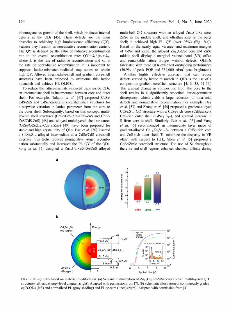
Song et al. [7] designed a Zn1-xCdxSe/ZnSe/ZnS alloyed
multishell QD structure with an alloyed Zn1-xCdxSe core,
ZnSe as the middle shell, and ultrathin ZnS as the outer
shell; it achieved high PL QY (over 95%) (Fig. 3(a)).
Based on the nearly equal valence-band-maximum energies
of CdSe and ZnSe, the alloyed Zn1-xCdxSe core and ZnSe
middle shell display a marginal valence-band (VB) offset
and remarkable lattice fringes without defects. QLEDs
fabricated with these QDs exhibited outstanding performance
(30.9% of peak EQE and 334,000 cd/m2 peak brightness).
Another highly effective approach that can reduce
defects caused by lattice mismatch in QDs is the use of a
composition-gradient core/shell structure [4, 6, 35, 51-54].
The gradual change in composition from the core to the
shell results in a significantly smoothed lattice-parameter
discrepancy, which yields a large reduction of interfacial
defects and nonradiative recombination. For example, Dey
et al. [53] and Zhang et al. [54] proposed a gradient-alloyed
CdSexS1-x QD structure with a CdSe-rich core (CdSe0.8S0.2),
CdS-rich outer shell (CdSe0.1S0.9), and gradual increase in
S from core to shell. Similarly, Bae et al. [35] and Yang
et al. [6] recommended an intermediate layer made of
gradient-alloyed Cd1-xZnxSe1-ySy between a CdSe-rich core
and ZnS-rich outer shell. To minimize the disparity in VB
offset with respect to HTL, Shen et al. [5] proposed a
CdSe/ZnSe core/shell structure. The use of Se throughout
the core and shell regions enhances chemical affinity during
FIG. 3. HL-QLEDs based on material modification. (a) Schematic illustration of Zn1-xCdxSe/ZnSe/ZnS alloyed multilayered QD
structure (left) and energy-level diagram (right). Adapted with permission from [7]. (b) Schematic illustration of continuously graded
cg/B-QDs (left) and normalized PL (gray shading) and EL spectra (lines) (right). Adapted with permission from [4].
Recent Progress in High-Luminance Quantum Dot Light-Emitting Diodes - Seunghyun Rhee et al. 165
atomistic growth, resulting in better interfacial properties
and a reduction in interfacial defects. The QLED based on
this type of QD exhibited high PL QY (>90% for red and
green, and 73% for blue) and remarkable device efficiency,
with maximum brightness of 356,000 cd/m2, 614,000 cd/m2,
and 62.600 cd/m2 for red, green, and blue respectively (the
brightness of these red and blue emissions being the highest
reported for QLEDs). The gradually varying chemical
composition (or energy) of QDs more or less relieves the
interfacial strain of the core/shell structure, and improves
the PL QY of QDs and performance of QLEDs. In addition,
Lim et al. [4] synthesized a CdSe/CdxZn1-xSe/ZnSeyS1-y
structure with a continuously graded (cg) CdxZn1-xSe inner
shell and a wide-gap ZnSeyS1-y barrier (B) layer. The inner
shell modifies the electron injection into the CdSe core
efficiently and enables development of an electron-confine-
ment structure, which can suppress Auger recombination.
Meanwhile, the outer barrier of the ZnSeyS1-y layer (varied
by y) controls the valance-band and conduction-band (CB)
edges of the QD. These eventually equalize the charge
injection rate from the CTL to the QD. Devices based on
cg/B-QDs exhibited high peak EQE (13.5%) and peak
brightness (319,003 cd/m2), and simultaneously accomplished
almost droop-free QLEDs (efficiency reduction of ~3% at
100,000 cd/m2) (see Fig. 3(b)).
In addition to the core/shell structure, the selection of
an appropriate surface ligand is important for achieving
high-QY QDs [55, 56]. Ligands play a significant role in
both the processability and conductivity of QDs. For
example, a long-hydrocarbon-chain ligand (e.g. oleic acid
or oleylamine) can straightforwardly prevent QD aggregation
in organic solvents, but the increased interdot distance can
worsen the charge-transport properties of the QD film.
Therefore, it is important to exchange long, insulating
hydrocarbon-chain ligands for short, conducting ligands,
without compromising on QY. To achieve high-QY QDs,
the ligand must have (ⅰ) a short chain length, to reduce the
insulation between the CTLs and QD layers, and (ⅱ) the
property of binding strongly to the QD surface, without
developing defect states.
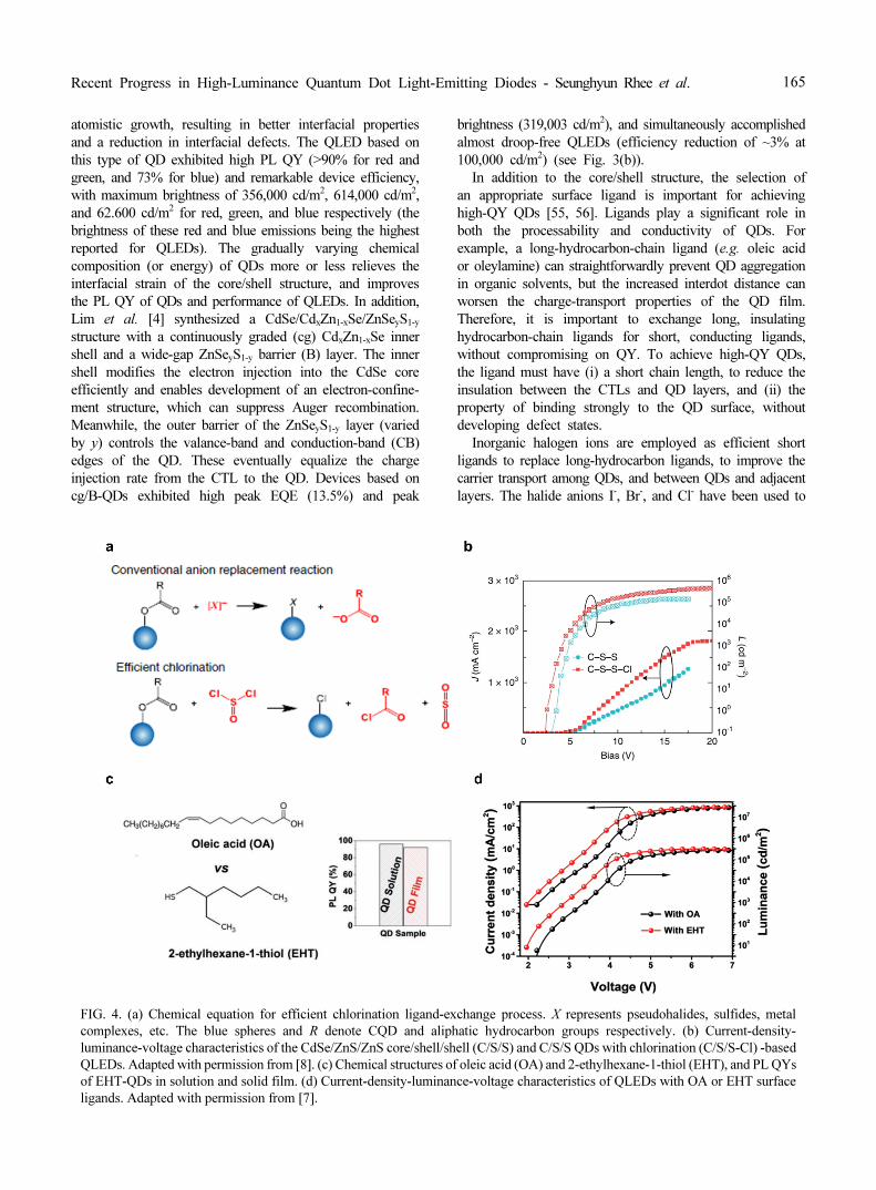
Inorganic halogen ions are employed as efficient short
ligands to replace long-hydrocarbon ligands, to improve the
carrier transport among QDs, and between QDs and adjacent
layers. The halide anions I-, Br-, and Cl- have been used to
FIG. 4. (a) Chemical equation for efficient chlorination ligand-exchange process. X represents pseudohalides, sulfides, metal
complexes, etc. The blue spheres and R denote CQD and aliphatic hydrocarbon groups respectively. (b) Current-density-
luminance-voltage characteristics of the CdSe/ZnS/ZnS core/shell/shell (C/S/S) and C/S/S QDs with chlorination (C/S/S-Cl) -based
QLEDs. Adapted with permission from [8]. (c) Chemical structures of oleic acid (OA) and 2-ethylhexane-1-thiol (EHT), and PL QYs
of EHT-QDs in solution and solid film. (d) Current-density-luminance-voltage characteristics of QLEDs with OA or EHT surface
ligands. Adapted with permission from [7].
Current Optics and Photonics, Vol. 4, No. 3, June 2020166
stabilize colloidal materials, control interdot distance, and
enhance the charge transport of QDs [57, 58]. Kang et al.
adopted a bromide (Br-) ligand using cetyltrimethylammonium
bromide (CTAB) treatment [58]. This short, conductive
ligand enhanced QD-film conductivity. Moreover, the
Br-QD-based LED exhibited increased brightness, without
decreased PL QY. Li et al. proposed an efficient chlorination
process that can effectively exchange long-hydrocarbon
OA ligands with conductive chloride (Cl-) ligands using a
chlorination reagent (SOCl2), as shown in Fig. 4(a) [8].
This inorganic single-atomic-layer surface ligand reduced
the interdot distance of QD films without compromising the
PL QY (63% and 60±2% for pristine QD film and Cl-QD
film respectively), and enhanced the charge-carrier transport
in Cl-QD-based devices. Efficient electron and hole injection
can suppress Auger recombination, particularly in the high-
current-density region, to result in a high peak brightness
of 460,000 cd/m2 in Cl-QD-based LEDs (Fig. 4(b)).
Owing to its strong binding property, thiol ligands are
also widely used as an effective ligand for high-performance
QLEDs. The thiol-type ligand, which has relatively short
chains for efficient carrier injection and strong anchoring
properties on the QD surface, is an electron-donor group
that can reduce the VBs of QDs and hole-injection barriers.
Shen et al. reported 1-octanethiol (OT) ligands on ZnCdS/
ZnS graded core/shell QDs, achieving the first reported
blue QLEDs with EQE higher than 10% [42]. Li et al. also
adopted tris (mercaptomethyl)-nonane (TMMN)-capped QDs,
which displayed a PL lifetime (9.3 ns) higher than that of
OA-capped QDs, owing to the reduced steric hindrance by
the shorter ligand chains [59]. Song et al. recommended the
2-ethylhexane-1-thiol (EHT) ligand on Zn1-xCdxSe/ZnSe/ZnS
core/shell QDs, which reduces hole injection barrier (between
HTL and QDs) from 1.18 eV to 0.91 eV and preserves the
high PL QY of QD films (~90%) (Figs. 4(c) and 4(d)) [7].
2.2. HL-QLEDs Based on Device Engineering
Apart from the high PL QY and conductivity of QD
materials, the adoption of appropriate device structure
significantly affects the achievement of HL-QLEDs. The
device structure, ETL, and HTL together determine the
carrier-injection properties, carrier confinement in a QD’s
emissive layer (EML), and the operational stability of
QLEDs. Balancing of the injection rates of electrons and
holes into the QD EML, and maintenance of operational
stability, are the key factors in achieving HL-QLEDs [25,
33, 60]. A disparity between electron and hole injection
rates induces nonradiative Auger recombination, resulting
in a reduction of the luminance efficiency of a QLED. In
addition, the overflow of majority carriers (electrons) to a
counter CTL (HTL) accelerates the degradation of organic
HTL materials, which attenuates the operational stability of
devices [25, 60]. Therefore, various approaches to improving
the charge-injection balance in QLEDs have been adopted,
in terms of device engineering.
Charge imbalance in QLEDs arises from the different
transport and injection capabilities of electrons and holes.
For example, ZnO nanoparticles (NPs), the most widely
used material for the ETL in a QLED, exhibit a CB
energy level highly similar to that of QDs, resulting in
straightforward (and occasionally spontaneous) injection of
electrons. In contrast, most of the organic hole-transport
materials used for the HTL, such as poly(9,9-dioctylfluorene-
co-N-(4-(3-methylpropyl))diphenylamine) (TFB), poly(N,N′-bis
(4-butylphenyl)-N,N′-bis(phenyl)-benzidine (poly-TPD), poly(9-
vinlycarbazole) (PVK), 4,4′-bis(carbazole-9-yl)biphenyl (CBP),
and Tris(4-carbazoyl-9-ylphenyl)amine (TCTA), exhibit a
large difference in VB energy level from that of QDs.
This disrupts efficient injection of holes. Furthermore, the
large difference between the electron mobility of ZnO NPs
and hole mobility of organic HTL materials worsens the
charge imbalance [61, 62]. Various strategies have been
recommended to alleviate this disparity, such as enhancing
hole injection by modifying the HTL [21, 23-25] and
reducing electron injection by ion doping [4, 63, 64] or by
inserting an electron-blocking layer (EBL) [19, 65-67].
However, suppressing electron injection results in increased
operational stress in QLEDs, so alternative approaches to
enhancing hole injection by modulating HTLs in the QLED
architecture have been proposed instead.
Unlike the straightforward electron injection/transport
using a ZnO NP ETL, hole injection/transport using organic
HTLs encounters several obstacles, owing to the large
difference in VB level versus QDs and relatively low hole
mobilities. Therefore, an inverted QLED structure, which
enables the use of deep-VB organic material for the HTL,
was proposed to enhance hole injection and device
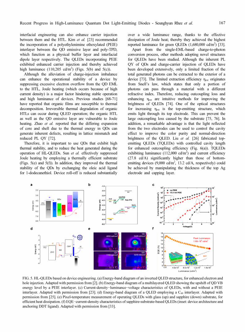
performance. Kwak et al. [2] devised the first inverted
QLED structure and the first HL-QLEDs exceeding 105
cd/m2. Subsequently, based on this structure several studies
were conducted to alleviate the remaining hole-injection
barrier in the inverted QLED structure (Fig. 5(a)). Rhee et
al. [25] reported the insertion of a thin fullerene (C60)
interlayer between the hole-injection layer (HIL, MoOx) and
HTL (CBP) to eliminate the universal hole-injection barrier
that is created by the pinning effect of MoOx (Fig. 5(d)).
Meanwhile, Jiang et al. [22] enhanced hole injection by
introducing a 4,4',4"-tri(N-carbazolyl)-triphenyl-amine (TCTA) /
N,N'-bis (naphthalen-1-yl)-N,N'-bis (phenyl)-benzidine (NPB)
bilayer HTL structure. This structure can be obtained
thanks to the high VB of TCTA and the high hole mobility
of NPB. Although most of the polymer HTLs used in the
conventional QLED structure exhibit a large VB difference
from QDs, various studies have been conducted to
overcome the hole-injection barrier. Combination of two
HTLs also can be an efficient method: For example,
Huang et al. [21] used a CBP-doped poly-TPD HTL,
which can deepen the VB energy level of poly-TPD.
Similarly, Li et al. [24] recommended the composition of
a TPD/PVK HTL structure, which improves hole mobility
with TPD and blocks electron suppression from the QD
emissive layer. Upshifting the energy level of the QDs by
Recent Progress in High-Luminance Quantum Dot Light-Emitting Diodes - Seunghyun Rhee et al. 167
interfacial engineering can also enhance carrier injection
between them and the HTL. Kim et al. [23] recommended
the incorporation of a polyethylenimine ethoxylated (PEIE)
interlayer between the QD emissive layer and poly-TPD,
which function as a physical buffer layer and interfacial
dipole layer respectively. The QLEDs incorporating PEIE
exhibited enhanced carrier injection and thereby achieved
high luminance (110,205 cd/m2) (Figs. 5(b) and 5(c)).
Although the alleviation of charge-injection imbalance
can enhance the operational stability of a device by
suppressing excessive electron overflow from the QD EML
to the HTL, Joule heating (which occurs because of high
current density) is a major factor hindering stable operation
and high luminance of devices. Previous studies [68-71]
have reported that organic films are susceptible to thermal
decomposition. Irreversible thermal degradation of organic
HTLs can occur during QLED operation; the organic HTL
as well as the QD emissive layer are vulnerable to Joule
heating. Zhao et al. reported that the differing expansion
of core and shell due to the thermal energy in QDs can
generate inherent defects, resulting in lattice mismatch and
reduced PL QY [72].
Therefore, it is important to use QDs that exhibit high
thermal stability, and to reduce the heat generated during the
operation of HL-QLEDs. Sun et al. effectively suppressed
Joule heating by employing a thermally efficient substrate
(Figs. 5(e) and 5(f)). In addition, they improved the thermal
stability of the QDs by exchanging the oleic acid ligand
for 1-dodecanethiol. Device roll-off is reduced substantially
over a wide luminance range, thanks to the effective
dissipation of Joule heat; thereby they achieved the highest
reported luminance for green QLEDs (1,680,000 cd/m2) [33].
Apart from the single-EML-based charge-to-photon
conversion process, other methods adopting novel structures
for QLEDs have been studied. Although the inherent PL
QY of QDs and charge-carrier injection of QLEDs have
been developed extensively, only a limited fraction of the
total generated photons can be extracted to the exterior of a
device [73]. The limited extraction efficiency ηext originates
from Snell’s law, which states that only a portion of
photons can pass through a material with a different
refractive index. Therefore, reducing outcoupling loss and
enhancing ηext are intuitive methods for improving the
brightness of QLEDs [74]. One of the optical structures
for increasing ηext is the top-emitting structure, which
emits light through its top electrode. This can prevent the
large outcoupling loss caused by the substrate [75, 76]. In
addition, a remarkable advantage is that the light reflected
from the two electrodes can be used to control the cavity
effect to improve the color purity and normal-direction
brightness of the QLED. Liu et al. [26] fabricated top-
emitting QLEDs (TQLEDs) with controlled cavity length
for enhanced outcoupling efficiency (Fig. 6(a)). TQLEDs
exhibiting luminance (112,000 cd/m2) and current efficiency
(27.8 cd/A) significantly higher than those of bottom-
emitting devices (9,000 cd/m2, 13.2 cd/A, respectively) could
be achieved by manipulating the thickness of the top Ag
electrode and capping layer.
FIG. 5. HL-QLEDs based on device engineering. (a) Energy-band diagram of an inverted QLED structure, for enhanced electron and
hole injection. Adapted with permission from [2]. (b) Energy-band diagram of a multilayered QLED showing the upshift of QD VB
energy level by a PEIE interlayer. (c) Current-density−luminance−voltage characteristics of QLEDs, with and without a PEIE
interlayer. Adapted with permission from [23]. (d) Energy-band diagram of a QLED employing a C60 interlayer. Adapted with
permission from [25]. (e) Pixel-temperature measurement of operating QLEDs with glass (up) and sapphire (down) substrate, for
efficient heat dissipation. (f) EQE−current-density characteristics of sapphire-substrate-based QLEDs (inset: device architecture and
anchoring DDT ligand). Adapted with permission from [33].
Current Optics and Photonics, Vol. 4, No. 3, June 2020168
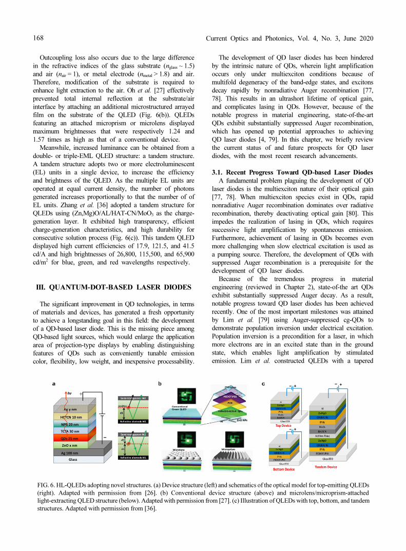
Outcoupling loss also occurs due to the large difference
in the refractive indices of the glass substrate (nglass ~ 1.5)
and air (nair = 1), or metal electrode (nmetal > 1.8) and air.
Therefore, modification of the substrate is required to
enhance light extraction to the air. Oh et al. [27] effectively
prevented total internal reflection at the substrate/air
interface by attaching an additional microstructured arrayed
film on the substrate of the QLED (Fig. 6(b)). QLEDs
featuring an attached microprism or microlens displayed
maximum brightnesses that were respectively 1.24 and
1.57 times as high as that of a conventional device.
Meanwhile, increased luminance can be obtained from a
double- or triple-EML QLED structure: a tandem structure.
A tandem structure adopts two or more electroluminescent
(EL) units in a single device, to increase the efficiency
and brightness of the QLED. As the multiple EL units are
operated at equal current density, the number of photons
generated increases proportionally to that the number of of
EL units. Zhang et al. [36] adopted a tandem structure for
QLEDs using (Zn,Mg)O/AL/HAT-CN/MoO3 as the charge-
generation layer. It exhibited high transparency, efficient
charge-generation characteristics, and high durability for
consecutive solution process (Fig. 6(c)). This tandem QLED
displayed high current efficiencies of 17.9, 121.5, and 41.5
cd/A and high brightnesses of 26,800, 115,500, and 65,900
cd/m2 for blue, green, and red wavelengths respectively.
III. QUANTUM-DOT-BASED LASER DIODES
The significant improvement in QD technologies, in terms
of materials and devices, has generated a fresh opportunity
to achieve a longstanding goal in this field: the development
of a QD-based laser diode. This is the missing piece among
QD-based light sources, which would enlarge the application
area of projection-type displays by enabling distinguishing
features of QDs such as conveniently tunable emission
color, flexibility, low weight, and inexpensive processability.
The development of QD laser diodes has been hindered
by the intrinsic nature of QDs, wherein light amplification
occurs only under multiexciton conditions because of
multifold degeneracy of the band-edge states, and excitons
decay rapidly by nonradiative Auger recombination [77,
78]. This results in an ultrashort lifetime of optical gain,
and complicates lasing in QDs. However, because of the
notable progress in material engineering, state-of-the-art
QDs exhibit substantially suppressed Auger recombination,
which has opened up potential approaches to achieving
QD laser diodes [4, 79]. In this chapter, we briefly review
the current status of and future prospects for QD laser
diodes, with the most recent research advancements.
3.1. Recent Progress Toward QD-based Laser Diodes
A fundamental problem plaguing the development of QD
laser diodes is the multiexciton nature of their optical gain
[77, 78]. When multiexciton species exist in QDs, rapid
nonradiative Auger recombination dominates over radiative
recombination, thereby deactivating optical gain [80]. This
impedes the realization of lasing in QDs, which requires
successive light amplification by spontaneous emission.
Furthermore, achievement of lasing in QDs becomes even
more challenging when slow electrical excitation is used as
a pumping source. Therefore, the development of QDs with
suppressed Auger recombination is a prerequisite for the
development of QD laser diodes.
Because of the tremendous progress in material
engineering (reviewed in Chapter 2), state-of-the art QDs
exhibit substantially suppressed Auger decay. As a result,
notable progress toward QD laser diodes has been achieved
recently. One of the most important milestones was attained
by Lim et al. [79] using Auger-suppressed cg-QDs to
demonstrate population inversion under electrical excitation.
Population inversion is a precondition for a laser, in which
more electrons are in an excited state than in the ground
state, which enables light amplification by stimulated
emission. Lim et al. constructed QLEDs with a tapered
FIG. 6. HL-QLEDs adopting novel structures. (a) Device structure (left) and schematics of the optical model for top-emitting QLEDs
(right). Adapted with permission from [26]. (b) Conventional device structure (above) and microlens/microprism-attached
light-extracting QLED structure (below). Adapted with permission from [27]. (c) Illustration of QLEDs with top, bottom, and tandem
structures. Adapted with permission from [36].
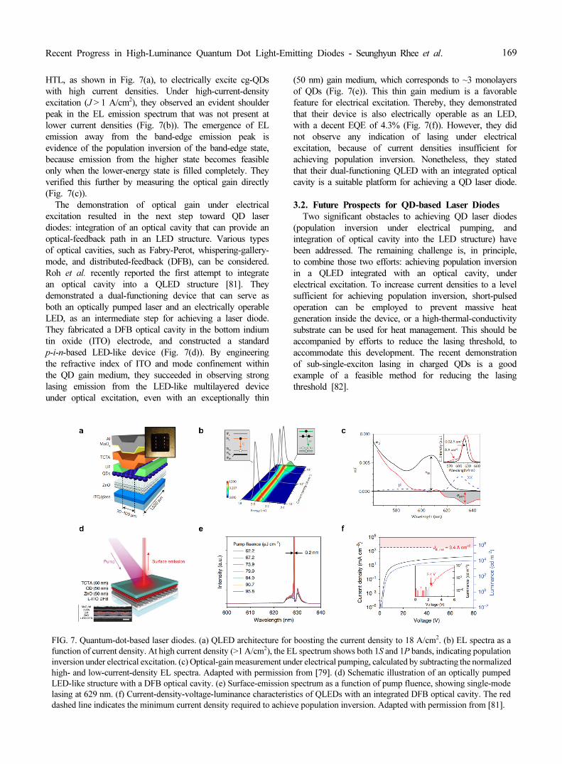
Recent Progress in High-Luminance Quantum Dot Light-Emitting Diodes - Seunghyun Rhee et al. 169
HTL, as shown in Fig. 7(a), to electrically excite cg-QDs
with high current densities. Under high-current-density
excitation (J > 1 A/cm2), they observed an evident shoulder
peak in the EL emission spectrum that was not present at
lower current densities (Fig. 7(b)). The emergence of EL
emission away from the band-edge emission peak is
evidence of the population inversion of the band-edge state,
because emission from the higher state becomes feasible
only when the lower-energy state is filled completely. They
verified this further by measuring the optical gain directly
(Fig. 7(c)).
The demonstration of optical gain under electrical
excitation resulted in the next step toward QD laser
diodes: integration of an optical cavity that can provide an
optical-feedback path in an LED structure. Various types
of optical cavities, such as Fabry-Perot, whispering-gallery-
mode, and distributed-feedback (DFB), can be considered.
Roh et al. recently reported the first attempt to integrate
an optical cavity into a QLED structure [81]. They
demonstrated a dual-functioning device that can serve as
both an optically pumped laser and an electrically operable
LED, as an intermediate step for achieving a laser diode.
They fabricated a DFB optical cavity in the bottom indium
tin oxide (ITO) electrode, and constructed a standard
p-i-n-based LED-like device (Fig. 7(d)). By engineering
the refractive index of ITO and mode confinement within
the QD gain medium, they succeeded in observing strong
lasing emission from the LED-like multilayered device
under optical excitation, even with an exceptionally thin
(50 nm) gain medium, which corresponds to ~3 monolayers
of QDs (Fig. 7(e)). This thin gain medium is a favorable
feature for electrical excitation. Thereby, they demonstrated
that their device is also electrically operable as an LED,
with a decent EQE of 4.3% (Fig. 7(f)). However, they did
not observe any indication of lasing under electrical
excitation, because of current densities insufficient for
achieving population inversion. Nonetheless, they stated
that their dual-functioning QLED with an integrated optical
cavity is a suitable platform for achieving a QD laser diode.
3.2. Future Prospects for QD-based Laser Diodes
Two significant obstacles to achieving QD laser diodes
(population inversion under electrical pumping, and
integration of optical cavity into the LED structure) have
been addressed. The remaining challenge is, in principle,
to combine those two efforts: achieving population inversion
in a QLED integrated with an optical cavity, under
electrical excitation. To increase current densities to a level
sufficient for achieving population inversion, short-pulsed
operation can be employed to prevent massive heat
generation inside the device, or a high-thermal-conductivity
substrate can be used for heat management. This should be
accompanied by efforts to reduce the lasing threshold, to
accommodate this development. The recent demonstration
of sub-single-exciton lasing in charged QDs is a good
example of a feasible method for reducing the lasing
threshold [82].
FIG. 7. Quantum-dot-based laser diodes. (a) QLED architecture for boosting the current density to 18 A/cm2. (b) EL spectra as a
function of current density. At high current density (>1 A/cm2), the EL spectrum shows both 1S and 1P bands, indicating population
inversion under electrical excitation. (c) Optical-gain measurement under electrical pumping, calculated by subtracting the normalized
high- and low-current-density EL spectra. Adapted with permission from [79]. (d) Schematic illustration of an optically pumped
LED-like structure with a DFB optical cavity. (e) Surface-emission spectrum as a function of pump fluence, showing single-mode
lasing at 629 nm. (f) Current-density-voltage-luminance characteristics of QLEDs with an integrated DFB optical cavity. The red
dashed line indicates the minimum current density required to achieve population inversion. Adapted with permission from [81].
Current Optics and Photonics, Vol. 4, No. 3, June 2020170
IV. SUMMARY
This paper has reviewed recent studies aimed at
overcoming the obstacles to achieving HL-QLEDs. The
status of the development of QD laser diodes was also
examined briefly. Various efforts to achieve HL-QLEDs, in
terms of material development and device engineering, have
been summarized. With regard to material development,
the construction of an appropriate QD core/shell structure
that can minimize lattice-mismatch-induced traps has been
the major focus of research. The use of alloyed or gradient
shell structures was observed to be the most efficient
method for developing highly luminescent QDs. In addition,
the selection of appropriate surface ligands also plays a
significant role in realizing high luminance in QDs. Short
ligands are preferred, so as not to distort charge transport
and injection. Strong chemical bonding with QDs is also
important for producing high-quality film with few surface
traps. In terms of device engineering, designing a device
architecture that can suppress nonradiative Auger recombi-
nation by improving charge balance has been the most
important research direction for achieving HL-QLEDs. In
addition, the moderation of Joule heating, improvement in
light-extraction efficiency, and use of tandem structures
have also exhibited their effectiveness in improving the
luminance of QLEDs.
Notwithstanding this notable progress, several issues
remain to be addressed. The first of these is the degraded
luminescence efficiency of QDs in films. Although QDs in
solution exhibited near-unity PL QY, the PL QY of a QD
film still displays considerable suppression, owing to the
inherent defects formed during fabrication, and nonradiative
Auger recombination by dot interaction. Another issue is
the development (or identification) of a better HTL material
with a higher hole mobility, closer VB to that of QDs,
and most importantly high thermal stability. Present HTL
technologies rely substantially on organic materials, but
diverse types of materials should be employed and
investigated. By solving those remaining challenges, the
domain of application for QD-based light sources will be
widened, offering fresh opportunities for a wide range of
display applications.
ACKNOWLEDGMENT
This study was supported by the Technology Innovation
Program (or Industrial Strategic Technology Development
Program) (No.10077471) funded by the Ministry of Trade,
Industry & Energy (MOTIE, Korea), and the National
Research Foundation of Korea (NRF) grant funded by the
Korea government (Ministry of Science and ICT) (No.
2020R1C1C1013079).
REFERENCES
1. W. K. Bae, J. Lim, D. Lee, M. Park, H. Lee, J. Kwak, K.
Char, C. Lee, and S. Lee, “R/G/B/natural white light thin
colloidal quantum dot-based light-emitting devices,” Adv.
Mater. 26, 6387-6393 (2014).
2. J. Kwak, W. K. Bae, D. Lee, I. Park, J. Lim, M. Park, H.
Cho, H. Woo, D. Y. Yoon, K. Char, S. Lee, and C. Lee,
“Bright and efficient full-color colloidal quantum dot light-
emitting diodes using an inverted device structure,” Nano
Lett. 12, 2362-2366 (2012).
3. S. J. Lim, M. U. Zahid, P. Le, L. Ma, D. Entenberg, A. S.
Harney, J. Condeelis, and A. M. Smith, “Brightness-equalized
quantum dots,” Nat. Commun. 6, 8210 (2015).
4. J. Lim, Y. S. Park, K. Wu, H. J. Yun, and V. I. Klimov,
“Droop-free colloidal quantum dot light-emitting diodes,”
Nano Lett. 18, 6645-6653 (2018).
5. H. Shen, Q. Gao, Y. Zhang, Y. Lin, Q. Lin, Z. Li, L.
Chen, Z. Zeng, X. Li, Y. Jia, S. Wang, Z. L. Du, L. S. Li,
and Z. Zhang, “Visible quantum dot light-emitting diodes
with simultaneous high brightness and efficiency,” Nat.
Photonics 13, 192-197 (2019).
6. Y. Yang, Y. Zheng, W. Cao, A. Titov, J. Hyvonen, J. R.
Manders, J. Xue, P. H. Holloway, and L. Qian, “High-
efficiency light-emitting devices based on quantum dots with
tailored nanostructures,” Nat. Photonics 9, 259-266 (2015).
7. J. Song, O. Wang, H. Shen, Q. Lin, Z. Li, L. Wang, X.
Zhang, and L. S. Li, “Over 30% external quantum efficiency
light-emitting diodes by engineering quantum dot-assisted
energy level match for hole transport layer,” Adv. Funct.
Mater. 29, 1808377 (2019).
8. X. Li, Y.-B. Zhao, F. Fan, L. Levina, M. Liu, R. Quintero-
Bermudez, X. Gong, L. N. Quan, J. Fan, Z. Yang, S.
Hoogland, O. Voznyy, Z.-H. Lu, and E. H. Sargent, “Bright
colloidal quantum dot light-emitting diodes enabled by
efficient chlorination,” Nat. Photonics 12, 159-164 (2018).
9. W. K. Bae, Y. S. Park, J. Lim, D. Lee, L. A. Padilha, H.
McDaniel, I. Robel, C. Lee, J. M. Pietryga, and V. I.
Klimov, “Controlling the influence of Auger recombination
on the performance of quantum-dot light-emitting diodes,”
Nat. Commun. 4, 2661 (2013).
10. J. M. Pietryga, Y.-S. Park, J. Lim, A. F. Fidler, W. K. Bae,
S. Brovelli, and V. I. Klimov, “Spectroscopic and device
aspects of nanocrystal quantum dots,” Chem. Rev. 116,
10513-10622 (2016).
11. W. K. Bae and J. Lim, “Nanostructured colloidal quantum
dots for efficient electroluminescence devices,” Korean J.
Chem. Eng. 36, 173-185 (2019).
12. C. Y. Han and H. Yang, “Development of colloidal quantum
dots for electrically driven light-emitting devices,” J. Korean
Ceram. Soc. 54, 449-469 (2017).
13. Y. Shang and Z. Ning, “Colloidal quantum-dots surface and
device structure engineering for high-performance light-
emitting diodes,” Natl. Sci. Rev. 4, 170-183 (2017).
14. M. K. Choi, J. Yang, T. Hyeon, and D.-H. Kim, “Flexible
quantum dot light-emitting diodes for next-generation
displays,” npj Flexible Electron. 2, 10 (2018).
15. F. Chen, Z. Guan, and A. Tang, “Nanostructure and device
architecture engineering for high-performance quantum-dot
light-emitting diodes,” J. Mater. Chem. C 6, 10958-10981
Recent Progress in High-Luminance Quantum Dot Light-Emitting Diodes - Seunghyun Rhee et al. 171
(2018).
16. V. L. Colvin, M. C. Schlamp, and A. P. Alivisatos, “Light-
emitting-diodes made from cadmium selenide nanocrystals
and a semiconducting polymer,” Nature 370, 354-357 (1994).
17. S. Coe, W. K. Woo, M. Bawendi, and V. Bulovic, “Electro-
luminescence from single monolayers of nanocrystals in
molecular organic devices,” Nature 420, 800-803 (2002).
18. A. H. Mueller, M. A. Petruska, M. Achermann, D. J.
Werder, E. A. Akhadov, D. D. Koleske, M. A. Hoffbauer,
and V. I. Klimov, “Multicolor light-emitting diodes based
on semiconductor nanocrystals encapsulated in GaN charge
injection layers,” Nano Lett. 5, 1039-1044 (2005).
19. X. Dai, Z. Zhang, Y. Jin, Y. Niu, H. Cao, X. Liang, L.
Chen, J. Wang, and X. Peng, “Solution-processed, high-
performance light-emitting diodes based on quantum dots,”
Nature 515, 96-99 (2014).
20. J. Lim, S. Jun, E. Jang, H. Baik, H. Kim, and J. Cho,
“Preparation of highly luminescent nanocrystals and their
application to light-emitting diodes,” Adv. Mater. 19, 1927-
1932 (2007).
21. Q. Huang, J. Pan, Y. Zhang, J. Chen, Z. Tao, C. He, K.
Zhou, Y. Tu, and W. Lei, “High-performance quantum dot
light-emitting diodes with hybrid hole transport layer via
doping engineering,” Opt. Express 24, 25955-25963 (2016).
22. C. Jiang, H. Liu, B. Liu, Z. Zhong, J. Zou, J. Wang, L.
Wang, J. Peng, and Y. Cao, “Improved performance of
inverted quantum dots light emitting devices by introducing
double hole transport layers,” Org. Electron. 31, 82-89 (2016).
23. D. Kim, Y. Fu, S. Kim, W. Lee, K.-H. Lee, H. K. Chung,
H.-J. Lee, H. Yang, and H. Chae, “Polyethylenimine
ethoxylated-mediated all-solution-processed high-performance
flexible inverted quantum dot-light-emitting device,” ACS
Nano 11, 1982-1990 (2017).
24. J. Li, Z. Liang, Q. Su, H. Jin, K. Wang, G. Xu, and X.
Xu, “Small molecule-modified hole transport layer targeting
low turn-on-voltage, bright, and efficient full-color quantum
dot light emitting diodes,” ACS Appl. Mater. Interfaces 10,
3865-3873 (2018).
25. S. Rhee, J. H. Chang, D. Hahm, K. Kim, B. G. Jeong, H.
J. Lee, J. Lim, K. Char, C. Lee, and W. K. Bae, ““Positive
incentive” approach to enhance the operational stability of
quantum dot-based light-emitting diodes,” ACS Appl. Mater.
Interfaces 11, 40252-40259 (2019).
26. G. Liu, X. Zhou, and S. Chen, “Very bright and efficient
microcavity top-emitting quantum dot light-emitting diodes
with Ag electrodes,” ACS Appl. Mater. Interfaces 8, 16768-
16775 (2016).
27. J. H. Oh, D. B. Choi, K. H. Lee, H. Yang, and Y. R. Do,
“Enhanced light extraction from green quantum dot light-
emitting diodes by attaching microstructure arrayed films,”
IEEE J. Sel. Top. Quantum Electron. 22, 42-47 (2016).
28. K. Ding, Y. Fang, S. Dong, H. Chen, B. Luo, K. Jiang, H.
Gu, L. Fan, S. Liu, B. Hu, and L. Wang, “24.1% external
quantum efficiency of flexible quantum dot light-emitting
diodes by light extraction of silver nanowire transparent
electrodes,” Adv. Opt. Mater. 6, 1800347 (2018).
29. B. S. Mashford, M. Stevenson, Z. Popovic, C. Hamilton,
Z. Zhou, C. Breen, J. Steckel, V. Bulovic, M. Bawendi, S.
Coe-Sullivan, and P. T. Kazlas, “High-efficiency quantum-dot
light-emitting devices with enhanced charge injection,” Nat.
Photonics 7, 407-412 (2013).
30. L. Wang, J. Lin, Y. Hu, X. Guo, Y. Lv, Z. Tang, J. Zhao,
Y. Fan, N. Zhang, Y. Wang, and X. Liu, “Blue quantum dot
light-emitting diodes with high electroluminescent efficiency,”
ACS Appl. Mater. Interfaces 9, 38755-38760 (2017).
31. Y. Fu, W. Jiang, D. Kim, W. Lee, and H. Chae, “Highly
efficient and fully solution-processed inverted light-emitting
diodes with charge control interlayers,” ACS Appl. Mater.
Interfaces 10, 17295-17300 (2018).
32. Y.-H. Won, O. Cho, T. Kim, D.-Y. Chung, T. Kim, H.
Chung, H. Jang, J. Lee, D. Kim, and E. Jang, “Highly
efficient and stable InP/ZnSe/ZnS quantum dot light-emitting
diodes,” Nature 575, 634-638 (2019).
33. Y. Sun, Q. Su, H. Zhang, F. Wang, S. Zhang, and S. Chen,
“Investigation on thermally induced efficiency roll-off:
toward efficient and ultrabright quantum-dot light-emitting
diodes,” ACS Nano 13, 11433-11442 (2019).
34. Y. Altintas, S. Genc, M. Y. Talpur, and E. Mutlugun,
“CdSe/ZnS quantum dot films for high performance flexible
lighting and display applications,” Nanotechnology 27,
295604 (2016).
35. W. K. Bae, K. Char, H. Hur, and S. Lee, “Single-step
synthesis of quantum dots with chemical composition
gradients,” Chem. Mat. 20, 531-539 (2008).
36. H. Zhang, S. Chen, and X. W. Sun, “Efficient red/green/
blue tandem quantum-dot light-emitting diodes with external
quantum efficiency exceeding 21%,” ACS Nano 12, 697-704
(2018).
37. Q. Sun, Y. A. Wang, L. S. Li, D. Wang, T. Zhu, J. Xu,
C. Yang, and Y. Li, “Bright, multicoloured light-emitting
diodes based on quantum dots,” Nat. Photonics 1, 717-722
(2007).
38. K.-S. Cho, E. K. Lee, W.-J. Joo, E. Jang, T.-H. Kim, S. J.
Lee, S.-J. Kwon, J. Y. Han, B. K. Kim, B. L. Choi, and J.
M. Kim, “High-performance crosslinked colloidal quantum-
dot light-emitting diodes,” Nat. Photonics 3, 341-345 (2009).
39. L. Qian, Y. Zheng, J. Xue, and P. H. Holloway, “Stable
and efficient quantum-dot light-emitting diodes based on
solution-processed multilayer structures,” Nat. Photonics 5,
543-548 (2011).
40. J. Lim, B. G. Jeong, M. Park, J. K. Kim, J. M. Pietryga,
Y.-S. Park, V. I. Klimov, C. Lee, D. C. Lee, and W. K.
Bae, “Influence of shell thickness on the performance of
light-emitting devices based on CdSe/Zn1-XCdXS core/shell
heterostructured quantum dots,” Adv. Mater. 26, 8034-8040
(2014).
41. J.-M. Caruge, J. E. Halpert, V. Bulović, and M. G. Bawendi,
“NiO as an inorganic hole-transporting layer in quantum-dot
light-emitting devices,” Nano Lett. 6, 2991-2994 (2006).
42. H. Shen, W. Cao, N. T. Shewmon, C. Yang, L. S. Li, and
J. Xue, “High-efficiency, low turn-on voltage blue-violet
quantum-dot-based light-emitting diodes,” Nano Lett. 15,
1211-1216 (2015).
43. H. Zhang, X. Sun, and S. Chen, “Over 100 cd A-1 efficient
quantum dot light-emitting diodes with inverted tandem
structure,” Adv. Funct. Mater. 27, 1700610 (2017).
44. B. O. Dabbousi, J. Rodriguez-Viejo, F. V. Mikulec, J. R.
Heine, H. Mattoussi, R. Ober, K. F. Jensen, and M. G.
Bawendi, “(CdSe) ZnS core-shell quantum dots: synthesis
and characterization of a size series of highly luminescent
Current Optics and Photonics, Vol. 4, No. 3, June 2020172
nanocrystallites,” J. Phys. Chem. B 101, 9463-9475 (1997).
45. X. Peng, M. C. Schlamp, A. V. Kadavanich, and A. P.
Alivisatos, “Epitaxial growth of highly luminescent CdSe/CdS
core/shell nanocrystals with photostability and electronic
accessibility,” J. Am. Chem. Soc. 119, 7019-7029 (1997).
46. D. V. Talapin, A. L. Rogach, A. Kornowski, M. Haase, and
H. Weller, “Highly luminescent monodisperse CdSe and
CdSe/ZnS nanocrystals synthesized in a hexadecylamine-
trioctylphosphine oxide-trioctylphospine mixture,” Nano Lett.
1, 207-211 (2001).
47. D. V. Talapin, I. Mekis, S. Götzinger, A. Kornowski, O.
Benson, and H. Weller, “CdSe/CdS/ZnS and CdSe/ZnSe/ZnS
core-shell-shell nanocrystals,” J. Phys. Chem. B 108, 18826-
18831 (2004).
48. E. Jang, S. Jun, H. Jang, J. Llim, B. Kim, and Y. Kim,
“White-light-emitting diodes with quantum dot color
converters for display backlights,” Adv. Mater. 22, 3076-3080
(2010).
49. R. Xie, U. Kolb, J. Li, T. Basché, and A. Mews, “Synthesis
and characterization of highly luminescent CdSe-Core CdS/
Zn0.5Cd0.5S/ZnS multishell nanocrystals,” J. Am. Chem. Soc.
127, 7480-7488 (2005).
50. W. K. Bae, L. A. Padilha, Y. S. Park, H. McDaniel, I.
Robel, J. M. Pietryga, and V. I. Klimov, “Controlled alloying
of the core-shell interface in CdSe/CdS quantum dots for
suppression of auger recombination,” ACS Nano 7, 3411-
3419 (2013).
51. J. Lim, M. Park, W. K. Bae, D. Lee, S. Lee, C. Lee, and
K. Char, “Highly efficient cadmium-free quantum dot light-
emitting diodes enabled by the direct formation of excitons
within InP@ZnSeS quantum dots,” ACS Nano 7, 9019-9026
(2013).
52. R. E. Bailey and S. Nie, “Alloyed semiconductor quantum
dots: Tuning the optical properties without changing the
particle size,” J. Am. Chem. Soc. 125, 7100-7106 (2003).
53. S. Dey, S. Chen, S. Thota, M. R. Shakil, S. L. Suib, and
J. Zhao, “Effect of gradient alloying on photoluminescence
blinking of single CdSxSe1-x nanocrystals,” J. Phys. Chem.
C 120, 20547-20554 (2016).
54. J. Zhang, Q. Yang, H. Cao, C. I. Ratcliffe, D. Kingston,
Q. Y. Chen, J. Ouyang, X. Wu, D. M. Leek, F. S. Riehle,
and K. Yu, “Bright gradient-alloyed CdSexS1-x quantum dots
exhibiting cyan-blue emission,” Chem. Mater. 28, 618-625
(2016).
55. D. Kim and D. C. Lee, “Surface ligands as permeation
barrier in the growth and assembly of anisotropic semi-
conductor nanocrystals,” J. Phys. Chem. Lett. 11, 2647-2657
(2020).
56. H. Lee, D.-E. Yoon, S. Koh, M. S. Kang, J. Lim, and D. C.
Lee, “Ligands as a universal molecular toolkit in synthesis
and assembly of semiconductor nanocrystals,” Chem. Sci.
11, 2318-2329 (2020).
57. H. Zhang, J. Jang, W. Liu, and D. V. Talapin, “Colloidal
nanocrystals with inorganic halide, pseudohalide, and halo-
metallate ligands,” ACS Nano 8, 7359-7369 (2014).
58. B.-H. Kang, J.-S. Lee, S.-W. Lee, S.-W. Kim, J.-W. Lee,
S.-A. Gopalan, J.-S. Park, D.-H. Kwon, J.-H. Bae, H.-R.
Kim, and S.-W. Kang, “Efficient exciton generation in
atomic passivated CdSe/ZnS quantum dots light-emitting
devices,” Sci. Rep. 6, 34659 (2016).
59. Z. Li, Y. Hu, H. Shen, Q. Lin, L. Wang, H. Wang, W.
Zhao, and L. S. Li, “Efficient and long-life green light-
emitting diodes comprising tridentate thiol capped quantum
dots,” Laser Photon. Rev. 11, 1600227 (2017).
60. J. H. Chang, P. Park, H. Jung, B. G. Jeong, D. Hahm, G.
Nagamine, J. Ko, J. Cho, L. A. Padilha, D. C. Lee, C.
Lee, K. Char, and W. K. Bae, “Unraveling the origin of
operational instability of quantum dot based light-emitting
diodes,” ACS Nano 12, 10231-10239 (2018).
61. H. Shen, Q. Lin, W. Cao, C. Yang, N. T. Shewmon, H.
Wang, J. Niu, L. S. Li, and J. Xue, “Efficient and long-
lifetime full-color light-emitting diodes using high lumine-
scence quantum yield thick-shell quantum dots,” Nanoscale
9, 13583-13591 (2017).
62. X. Xiong, C. Wei, L. Xie, M. Chen, P. Tang, W. Shen, Z.
Deng, X. Li, Y. Duan, W. Su, H. Zeng, and Z. Cui,
“Realizing 17.0% external quantum efficiency in red
quantum dot light-emitting diodes by pursuing the ideal
inkjet-printed film and interface,” Org. Electron. 73, 247-254
(2019).
63. Y. Lee, B. G. Jeong, H. Roh, J. Roh, J. Han, D. C. Lee,
W. K. Bae, J. Y. Kim, and C. Lee, “Enhanced lifetime and
efficiency of red quantum dot light-emitting diodes with
Y-doped ZnO sol-gel electron-transport layers by reducing
excess electron injection,” Adv. Quantum Technol. 1, 1700006
(2018).
64. J.-H. Kim, C.-Y. Han, K.-H. Lee, K.-S. An, W. Song, J.
Kim, M. S. Oh, Y. R. Do, and H. Yang, “Performance
improvement of quantum dot-light-emitting diodes enabled
by an alloyed ZnMgO nanoparticle electron transport layer,”
Chem. Mater. 27, 197-204 (2015).
65. X. Jin, C. Chang, W. Zhao, S. Huang, X. Gu, Q. Zhang,
F. Li, Y. Zhang, and Q. Li, “Balancing the electron and
hole transfer for efficient quantum dot light-emitting diodes
by employing a versatile organic electron-blocking layer,”
ACS Appl. Mater. Interfaces 10, 15803-15811 (2018).
66. Z. Li, “Enhanced performance of quantum dots light-emitting
diodes: The case of Al2O3 electron blocking layer,” Vacuum
137, 38-41 (2017).
67. I. Cho, H. Jung, B. G. Jeong, J. H. Chang, Y. Kim, K.
Char, D. C. Lee, C. Lee, J. Cho, and W. K. Bae, “Multi-
functional dendrimer ligands for high efficiency, solution-
processed quantum dot light-emitting diodes,” ACS Nano
11, 684-692 (2017).
68. J.-R. Gong, L.-J. Wan, S.-B. Lei, C.-L. Bai, X.-H. Zhang,
and S.-T. Lee, “Direct evidence of molecular aggregation
and degradation mechanism of organic light-emitting diodes
under joule heating: an STM and photoluminescence study,”
J. Phys. Chem. B 109, 1675-1682 (2005).
69. D. Y. Kondakov, W. C. Lenhart, and W. F. Nichols,
“Operational degradation of organic light-emitting diodes:
Mechanism and identification of chemical products,” J.
Appl. Phys. 101, 024512 (2007).
70. S. Schmidbauer, A. Hohenleutner, and B. König, “Chemical
degradation in organic light-emitting devices: mechanisms
and implications for the design of new materials,” Adv.
Mater. 25, 2114-2129 (2013).
71. K. Yoshida, T. Matsushima, Y. Shiihara, H. Kuwae, J.
Mizuno, and C. Adachi, “Joule heat-induced breakdown of
organic thin-film devices under pulse operation,” J. Appl.
Recent Progress in High-Luminance Quantum Dot Light-Emitting Diodes - Seunghyun Rhee et al. 173
Phys. 121, 195503 (2017).
72. Y. Zhao, C. Riemersma, F. Pietra, R. Koole, C. D. Donegá,
and A. Meijerink, “High-temperature luminescence quenching
of colloidal quantum dots,” ACS Nano 6, 9058-9067 (2012).
73. Q. Yue, W. Li, F. Kong, and K. Li, “Enhancing the out-
coupling efficiency of organic light-emitting diodes using
two-dimensional periodic nanostructures,” Adv. Mater. Sci.
Eng. 2012, 985762 (2012).
74. W. D. Kim, D. Kim, D.-E. Yoon, H. Lee, J. Lim, W. K.
Bae, and D. C. Lee, “Pushing the efficiency envelope for
semiconductor nanocrystal-based electroluminescence devices
using anisotropic nanocrystals,” Chem. Mater. 31, 3066-3082
(2019).
75. G. W. Park, S. J. Lee, and J. H. Ko, “Comparison of out-
coupling efficiency between bottom-emission and top-emission
organic light-emitting diodes using FDTD simulation,” J.
Nanoelectron. Optoelectron. 11, 229-233 (2016).
76. S. Hofmann, M. Thomschke, B. Lüssem, and K. Leo,
“Top-emitting organic light-emitting diodes,” Opt. Express
19, A1250-A1264 (2011).
77. V. I. Klimov, A. A. Mikhailovsky, S. Xu, A. Malko, J. A.
Hollingsworth, C. A. Leatherdale, H. J. Eisler, and M. G.
Bawendi, “Optical gain and stimulated emission in nano-
crystal quantum dots,” Science 290, 314-317 (2000).
78. F. Fan, O. Voznyy, R. P. Sabatini, K. T. Bicanic, M. M.
Adachi, J. R. McBride, K. R. Reid, Y. S. Park, X. Li, A.
Jain, R. Quintero-Bermudez, M. Saravanapavanantham, M.
Liu, M. Korkusinski, P. Hawrylak, V. I. Klimov, S. J.
Rosenthal, S. Hoogland, and E. H. Sargent, “Continuous-
wave lasing in colloidal quantum dot solids enabled by
facet-selective epitaxy,” Nature 544, 75-79 (2017).
79. J. Lim, Y.-S. Park, and V. I. Klimov, “Optical gain in
colloidal quantum dots achieved with direct-current electrical
pumping,” Nat. Mater. 17, 42-49 (2018).
80. Y. S. Park, W. K. Bae, T. Baker, J. Lim, and V. I. Klimov,
“Effect of auger recombination on lasing in heterostructured
quantum dots with engineered core/shell interfaces,” Nano
Lett. 15, 7319-7328 (2015).
81. J. Roh, Y.-S. Park, J. Lim, and V. I. Klimov, “Optically
pumped colloidal-quantum-dot lasing in LED-like devices
with an integrated optical cavity,” Nat. Commun. 11, 271
(2020).
82. O. V. Kozlov, Y.-S. Park, J. Roh, I. Fedin, T. Nakotte,
and V. I. Klimov, “Sub-single-exciton lasing using charged
quantum dots coupled to a distributed feedback cavity,”
Science 365, 672-675 (2019).