Embed Size (px)
Citation preview
Agilent 81250 ParBERT Applications
Recirculating Optical Loop Tests
S1
Important Notice
© Agilent Technologies, Inc. 2003
Manual PartNumber
5988-8675EN
Revision
Revision 1.0, February 2003
Printed in Germany
Agilent TechnologiesHerrenberger Straße 130D-71034 BöblingenGermany
Authors: t3 medien GmbH
Warranty
The material contained in this document is provided "as is," and is subject to being changed, without notice, in future editions. Further, to the maximum extent permitted by applicable law, Agilent disclaims all warranties, either express or implied, with regard to this manual and any information contained herein, including but not limited to the implied warranties of merchantability and fitness for a particular purpose. Agilent shall not be liable for errors or for incidental or consequential damages in connection with the furnishing, use, or performance of this document or of any information contained herein. Should Agilent and the user have a separate written agreement with warranty terms covering the material in this document that conflict with these terms, the warranty terms in the separate agreement shall control.
Technology Licenses
The hardware and/or software described in this document are furnished under a license and may be used or copied only in accordance with the terms of such license.
Restricted Rights Legend
If software is for use in the performance of a U.S. Government prime contract or subcontract, Software is delivered and licensed as "Commercial computer software" as defined in DFAR 252.227-7014 (June 1995), or as a "commercial item" as defined in FAR 2.101(a) or as "Restricted computer software" as defined in FAR 52.227-19 (June 1987) or any equivalent agency regulation or contract clause. Use, duplication or disclosure of Software is subject to Agilent Technologies' standard commercial license terms, and non-DOD Departments and Agencies of the U.S. Government will receive no greater than Restricted Rights as defined in FAR 52.227-19(c)(1-2) (June 1987). U.S. Government users will receive no greater than Limited Rights as defined in FAR 52.227-14 (June 1987) or DFAR 252.227-7015 (b)(2) (November 1995), as applicable in any technical data.
Safety Notices
CAUTION
A CAUTION notice denotes a hazard. It calls attention to an operating procedure, practice, or the like that, if not correctly performed or adhered to, could result in damage to the product or loss of important data. Do not proceed beyond a CAUTION notice until the indicated conditions are fully understood and met.
WARNING
A WARNING notice denotes a hazard. It calls attention to an operating procedure, practice, or the like that, if not correctly performed or adhered to, could result in personal injury or death. Do not proceed beyond a WARNING notice until the indicated conditions are fully understood and met.
2 Agilent 81250 ParBERT Applications, Recirculating Optical Loop Tests, February 2003
Contents
Contents
Application Overview 5
What are Recirculating Optical Loop Tests 6
General Considerations 9
Measurement Precision and Test Duration 9
The Loop Switch 10
Test Control 12
Analyzer Synchronization 13
Interdependences 15
Principle of Timing Calculations 15
Burst Mode Timing Calculation Example 16
Continuous Mode Timing Calculation Example 18
ParBERT Specials 19
Test Environment 20
Prerequisites 21
Configuration Examples with External Test Control 22
Prerequisites for Test Control 25
Test Control via External Equipment 25
Test Control via ParBERT Modules 25
Configuration Examples with Internal Test Control 26
Test Setup Procedures 29
General Procedure 30
Analyzer System Setup 33
Sequence for Pure Analyzer Operation 34
Sequence for Test Control via ParBERT 36
Agilent 81250 ParBERT Applications, Recirculating Optical Loop Tests, February 2003 3
Contents
Setting up a 40 Gbit/s Optical Loop Test 41
Focus of this Example 42
Hardware Setup 43
Pattern Generator Setup 45
Setting the Output Characteristics 46
Specifying the Generator Sequence 47
Pattern Analyzer Setup 50
Setting Up the Analyzer System Clock 52
Setting the Analyzer Sampling Delays 54
Specifying the Analyzer Test Sequence 63
Running the Test 65
Concluding Remarks 66
4 Agilent 81250 ParBERT Applications, Recirculating Optical Loop Tests, February 2003
Application Overview
This manual explains how the Agilent 81250 Parallel Bit Error Ratio Tester can be used for performing recirculating optical loop tests.
Focus of this manual The focus of this manual is on how to set up Agilent 81250 ParBERT systems for performing such tests successfully.
Since there are no standards for recirculating optical loop tests, this manual can only give general advice. But it may help you to solve your problem, and it shows a working example at 40 Gbit/s.
Reader assumptions Readers should have a basic understanding of data transmission through optical fibers and some experience with electro-optical equipment.
Readers should also have some experience with the use of Agilent 81250 ParBERT systems. They should be familiar with the ParBERT online help and the Agilent 81250 ParBERT System User Guide.
Additional software support The ParBERT Measurement Software also greatly supports the analysis of received data. It provides tools for measuring the eye opening, timing and jitter characteristics, signal levels, and more. For details please refer to the ParBERT Measurement Software documentation.
Literature This manual explains not only the generic ParBERT setup procedures but also describes a special assembly of electrically controlled optical switches—the EMI loop switch.
The EMI loop switch was developed at the Department of Electromagnetic Systems (EMI) of the Technical University of Denmark.
Details on the EMI loop switch and the EMI loop experiment have been published in:
Morten Nissov, "Long-Haul Optical Transmission Using Distributed Raman Amplification", Ph.D. Thesis, Department of Electromagnetic Systems, Technical University of Denmark, LD135, December 1997 (201 pages).
Agilent 81250 ParBERT Applications, Recirculating Optical Loop Tests, February 2003 5
Application Overview What are Recirculating Optical Loop Tests
What are Recirculating Optical Loop Tests
We are dealing with optical data transmission. The characteristics of light sources, glass fibers, and optical receivers have been investigated for many years. However, measuring and predicting the bit error rate of a long distance optical link (including the source, cables, connectors, amplifiers, signal conditioners, and so on) is still a challenge.
NO TE Recirculating optical loop tests are a method for simulating long distance optical links in a laboratory.
Measurement principle The principle is simple:
You feed an optical signal of limited duration into an optical link. This link may consist of a single fiber coil or several fiber coils with optical signal conditioners and amplifiers.
Then, you disconnect the source and allow the signal to circulate within a closed optical loop.
After a number of round-trips, you open or tap the loop and feed the circulating signal into a bit analyzer that compares the received data with expected data.
Once the loop has been emptied, you can repeat the test.
With this method and a carefully balanced electro-optical setup, optical signals have been observed and measured after distances of more than 7,000 km.
Measurement phases A recirculating optical loop test has at least three phases:
• Fill the loop
• Let the signal circulate
• Analyze and empty the loop
Some institutions differentiate between the analyzing and emptying phase.
6 Agilent 81250 ParBERT Applications, Recirculating Optical Loop Tests, February 2003
What are Recirculating Optical Loop Tests Application Overview
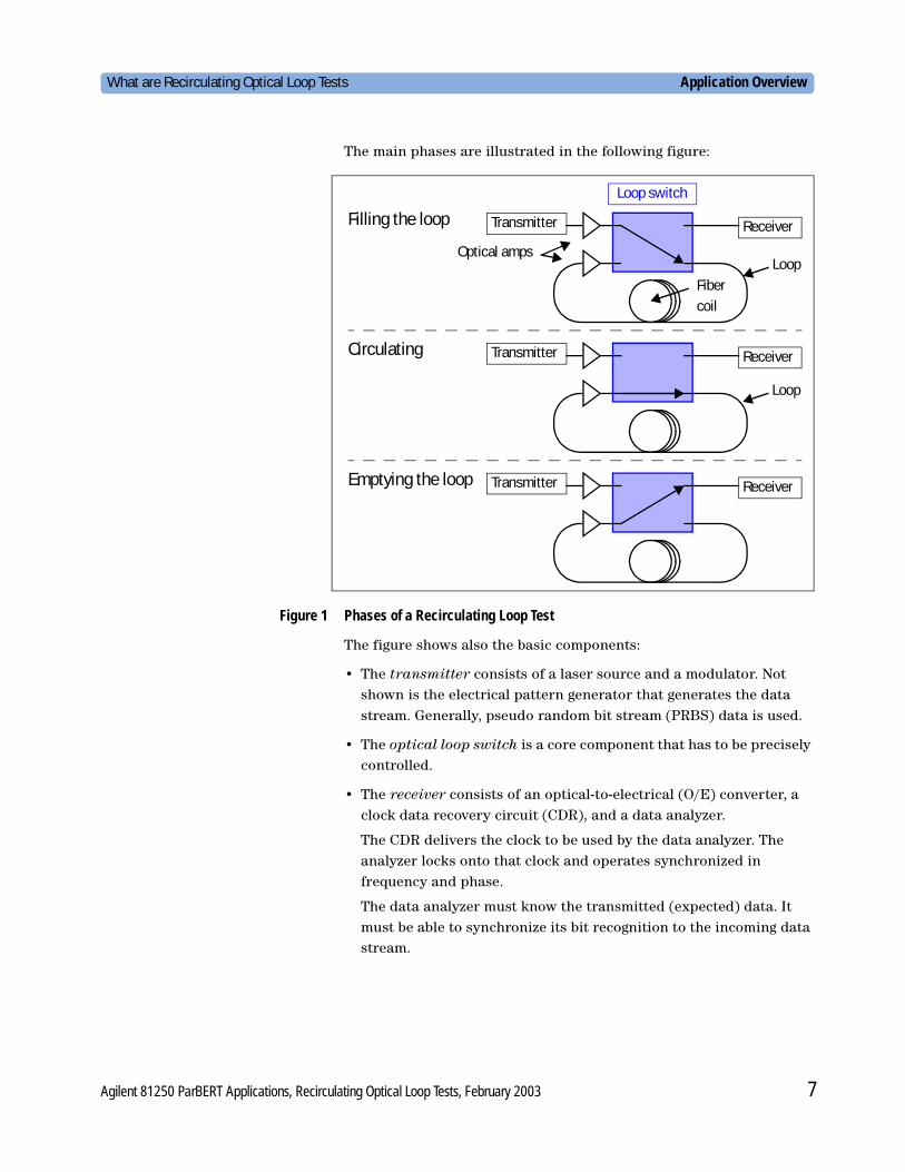
The main phases are illustrated in the following figure:
Figure 1 Phases of a Recirculating Loop Test
The figure shows also the basic components:
• The transmitter consists of a laser source and a modulator. Not shown is the electrical pattern generator that generates the data stream. Generally, pseudo random bit stream (PRBS) data is used.
• The optical loop switch is a core component that has to be precisely controlled.
• The receiver consists of an optical-to-electrical (O/E) converter, a clock data recovery circuit (CDR), and a data analyzer.
The CDR delivers the clock to be used by the data analyzer. The analyzer locks onto that clock and operates synchronized in frequency and phase.
The data analyzer must know the transmitted (expected) data. It must be able to synchronize its bit recognition to the incoming data stream.
Transmitter Receiver
Transmitter Receiver
Transmitter Receiver
Loop switch
Loop
Fiber
coil
Optical amps
Filling the loop
Circulating
Emptying the loop
Loop
Agilent 81250 ParBERT Applications, Recirculating Optical Loop Tests, February 2003 7
Application Overview What are Recirculating Optical Loop Tests
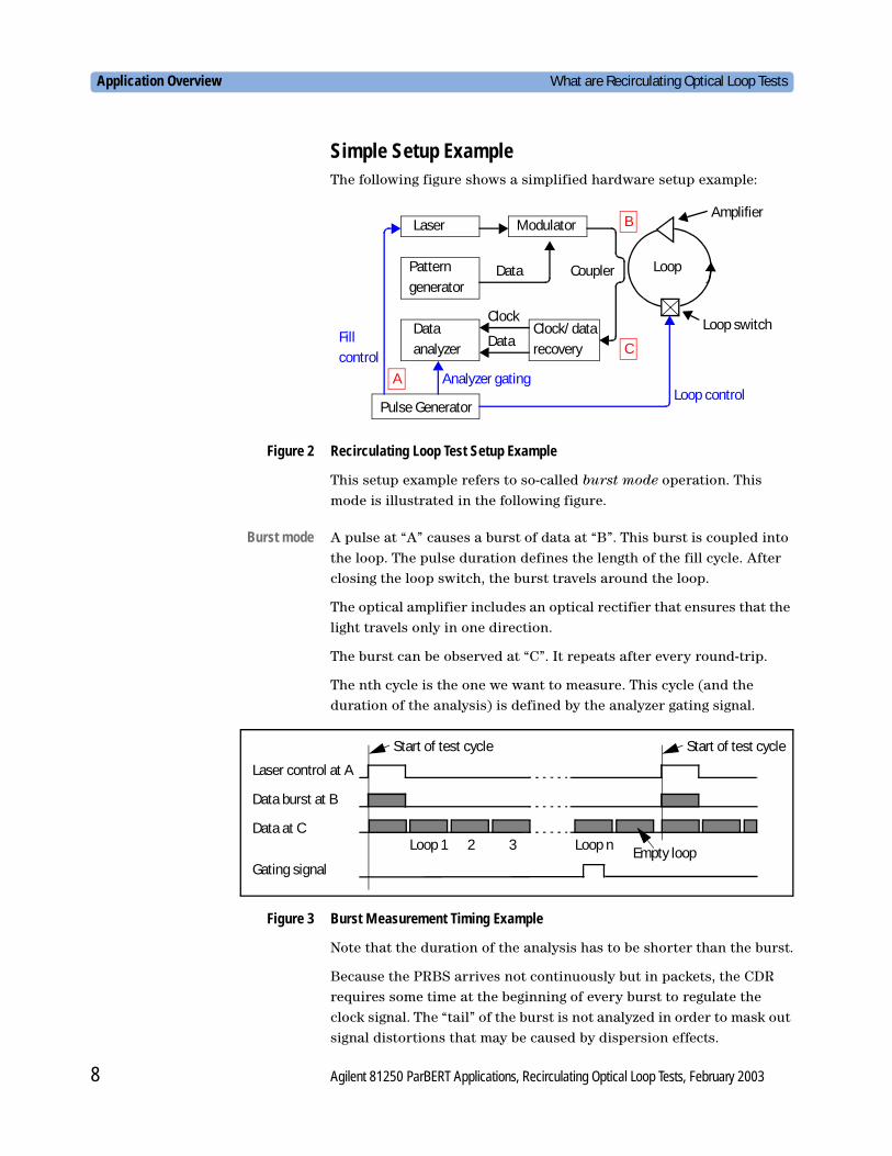
Simple Setup ExampleThe following figure shows a simplified hardware setup example:
Figure 2 Recirculating Loop Test Setup Example
This setup example refers to so-called burst mode operation. This mode is illustrated in the following figure.
Burst mode A pulse at “A” causes a burst of data at “B”. This burst is coupled into the loop. The pulse duration defines the length of the fill cycle. After closing the loop switch, the burst travels around the loop.
The optical amplifier includes an optical rectifier that ensures that the light travels only in one direction.
The burst can be observed at “C”. It repeats after every round-trip.
The nth cycle is the one we want to measure. This cycle (and the duration of the analysis) is defined by the analyzer gating signal.
Figure 3 Burst Measurement Timing Example
Note that the duration of the analysis has to be shorter than the burst.
Because the PRBS arrives not continuously but in packets, the CDR requires some time at the beginning of every burst to regulate the clock signal. The “tail” of the burst is not analyzed in order to mask out signal distortions that may be caused by dispersion effects.
DataPattern
generator
Modulator
Data
analyzer
Pulse Generator
Laser
Analyzer gating
Clock/data
recoveryData
Clock
LoopCoupler
Loop switch
A
B
C
Loop control
Fill
control
Amplifier
Laser control at A
Data burst at B
Data at CLoop 1 2 3 Loop n
Gating signal
Start of test cycle Start of test cycle
Empty loop
8 Agilent 81250 ParBERT Applications, Recirculating Optical Loop Tests, February 2003
General Considerations Application Overview
When the gating signal appears, the data analyzer first aligns its PRBS generator with the incoming data stream and then compares incoming data with expected data. When the gating signal ends, the analysis stops, and the result counters can be read.
After that, the loop can be emptied, refilled, and a new measurement cycle can begin.
General Considerations
This section explains a few points of general interest.
Measurement Precision and Test DurationYou need to compare around 1010 bits to measure a bit error rate of 10–9 reliably. But the number of bits you can circulate in a loop is limited by nature.
The phase velocity (sometimes called the speed of light) in glass with a refractive index of 1.5 is about 20 cm/ns. That means, the travelling time through a 50 km fiber coil is approximately 2.5 x 10⁵ ns or 250 µs.
Using a 10 Gbit/s generator, every bit requires 0.1 ns. That means, you can insert at most 2.5 x 106 bits into a 50 km loop. To simulate a distance of 5,000 km, this data block has to circulate 100 times.
To detect bit error rates down to 10–9, you have to repeat the measurement more than 1,000 times and to accumulate the results. Considering some overhead for data processing, measuring bit error rates of 10–12 reliably can take days.
This simple calculation explains why generators/analyzers below 10 Gbit/s are seldom used for such tests.
The duration of the test can be reduced by increasing the loop length (resulting, of course, in the need of additional optical amplifiers and equipment) and by using high-speed pattern generators and analyzers.
NOTE Compared to 10 Gbit/s generators/analyzers, the ParBERT 43/45G pattern generator/analyzer systems can reduce the test time to one fourth.
Agilent 81250 ParBERT Applications, Recirculating Optical Loop Tests, February 2003 9
Application Overview General Considerations
The Loop SwitchThe loop switch is a main component of the whole setup.
Burst mode, as explained in “Simple Setup Example” on page 8, requires only a simple on/off switch. But burst mode can be hard to control. Every new burst must circulate a number of times until stable conditions within the loop are reached, but the receiver timing has to be set up prior to the test.
Loop switch requirements In general, the loop switch has to fulfill the following tasks:
• Turn on the light of the transmitter until the loop is overfilled with data and optical amplifiers and components in the loop reach a steady state.
• Turn off the light of the transmitter and allow the signal to circulate.
• After the signal has circulated the desired number of times, open the loop and direct the signal to the receiver.
All these functions have to be performed with low insertion loss, low polarization effects, reproducible timing, and independently of the optical power and wavelength (which for this kind of tests is typically between 1530 and 1570 nm).
A couple of switch assemblies have been proposed, implemented, and tested at many research institutions. We will not dig into the details.
EMI loop switch The performance of the ParBERT 43/45G pattern generator/analyzer systems has been verified with the EMI loop switch, developed at the Department of Electromagnetic Systems (EMI) of the Technical University of Denmark.
This switch assembly consists basically of three acousto-optical modulators (AOMs).
• Two AOMs in series are used for connecting and completely disconnecting the transmitter to/from the loop. This yields an extinction ratio greater than 90 dB.
• A third AOM is used for closing and opening the loop.
10 Agilent 81250 ParBERT Applications, Recirculating Optical Loop Tests, February 2003
General Considerations Application Overview
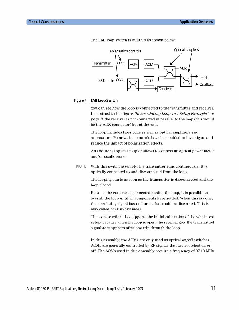
The EMI loop switch is built up as shown below:
Figure 4 EMI Loop Switch
You can see how the loop is connected to the transmitter and receiver. In contrast to the figure “Recirculating Loop Test Setup Example” on page 8, the receiver is not connected in parallel to the loop (this would be the AUX connector) but at the end.
The loop includes fiber coils as well as optical amplifiers and attenuators. Polarization controls have been added to investigate and reduce the impact of polarization effects.
An additional optical coupler allows to connect an optical power meter and/or oscilloscope.
NOTE With this switch assembly, the transmitter runs continuously. It is optically connected to and disconnected from the loop.
The looping starts as soon as the transmitter is disconnected and the loop closed.
Because the receiver is connected behind the loop, it is possible to overfill the loop until all components have settled. When this is done, the circulating signal has no bursts that could be discerned. This is also called continuous mode.
This construction also supports the initial calibration of the whole test setup, because when the loop is open, the receiver gets the transmitted signal as it appears after one trip through the loop.
In this assembly, the AOMs are only used as optical on/off switches. AOMs are generally controlled by RF signals that are switched on or off. The AOMs used in this assembly require a frequency of 27.12 MHz.
Transmitter AOM AOM
LoopAOMLoop
ReceiverOscillosc.
Optical couplersPolarization controls
AUX
Agilent 81250 ParBERT Applications, Recirculating Optical Loop Tests, February 2003 11
Application Overview General Considerations
Test ControlThe “Simple Setup Example” on page 8 shows a pulse generator for controlling the transmitter, the loop switch, and the data analyzer.
Unfortunately, the timing of the test phases can only be roughly estimated beforehand and has to be optimized under real-world conditions. This calls for computerized control.
Using ParBERT for generating and analyzing the data, you have three options:
• You can control ParBERT systems via electrical signals applied to the trigger pod.
• You can control ParBERT systems via their programming interface.
• You can use additional ParBERT modules/frontends for controlling the test phases.
Controlling ParBERT via Electrical SignalsThis approach corresponds to the setup of a standard serial bit error ratio tester (BERT). However, it requires programmable pulse generators (which are not really necessary), and inherent delays of the ParBERT hardware must be taken into account.
Controlling ParBERT by ProgrammingThis means, you write a program with your own user interface that controls the operation and timing of the generator and analyzer systems. SCPI and PNP commands are readily available.
Programmable events like CMD 0/1 can be used for controlling the ParBERT systems and the test flow.
Using ParBERT for Controlling the TestThis approach is the recommended solution. An additional low-speed ParBERT module built into the analyzer system with a few data generator frontends controls the optical switches.
This approach reduces the programming effort. The whole test can be set up, controlled, and optimized from the ParBERT user interface of the analyzer system. And reproducible timing relations are guaranteed.
12 Agilent 81250 ParBERT Applications, Recirculating Optical Loop Tests, February 2003
General Considerations Application Overview
A program is not required until the setup and timings have been verified and it comes to repeated measurements. Then, a simple program would read the bit and error counters, accumulate the results, and restart the test.
Analyzer SynchronizationBefore the bit error rate can be measured, the analyzer has to synchronize to the incoming data stream.
Analyzer synchronization consists of three steps:
• Frequency and phase synchronization
• Sampling point adjustment
• Alignment of received and expected data
Frequency and Phase SynchronizationClock recovery is the task of the clock data recovery (CDR) circuit (see also the figure “Recirculating Loop Test Setup Example” on page 8). The CDR can be a separate component or built into the analyzer.
NOTE ParBERT 43G/45G error detector systems have a built-in CDR circuit.
Data analyzers usually have a phase-locked loop (PLL) that locks onto the recovered clock. This happens once at the beginning of the test. All ParBERT systems can synchronize on the clock generated by an external CDR.
NOTE During the whole test, the CDR must deliver a continuous clock signal without interrupt. Otherwise the data analyzer would lose frequency and phase synchronization.
Sampling Point AdjustmentThe recovered clock phase of the analyzer system is usually not the optimum point in time for sampling the incoming signal. Sampling point adjustment means setting a suitable sampling delay with respect to the clock phase.
ParBERT data analyzers have a delay vernier that permits you to fine-tune the sampling point while a test is running. This vernier allows you to shift the sampling point by ±1 period.
Agilent 81250 ParBERT Applications, Recirculating Optical Loop Tests, February 2003 13
Application Overview General Considerations
Alignment of Received and Expected DataWhenever a burst of data comes in, the bit analyzer must adapt its expectation to the received data.
ParBERT systems provide two automated methods that can do both in one go—align received and expected data and set the optimum sampling delay. They are called Automatic Delay Alignment and Automatic Bit Synchronization. However, these methods are based on measuring the bit error rate and hence not suitable for the analysis of bursts that contain only a limited number of bits.
Fast Bit Synchronization Recirculating optical loop tests are generally performed with PRBS data. Particularly for the analysis of bursts holding PRBS data, an additional method has been implemented. It is called Fast Bit Synchronization.
Fast Bit Synchronization has no impact on the analyzer sampling point. The analyzer sampling point must be set and optimized beforehand.
Fast Bit Synchronization uses the very first incoming bits as a seed for the PRBS generator(s) built into the analyzer module(s). After that, the expected bit sequence corresponds to the received.
Fast Bit Synchronization can be used on all ParBERT analyzer systems, provided that PRBS/PRWS data is transmitted.
The number of bits needed for the alignment depends on two factors:
• The order of the PRBS polynomial
• The type of ParBERT data modules installed in the analyzer system
For details please refer to the section Principles of Analyzer Sampling Point Adjustment in the ParBERT System User Guide.
NO TE Fast Bit Synchronization always ends with “success”. By nature, it has no fail indicator that could be examined.
Fast Bit Synchronization requires that the very first incoming bits are correctly transmitted and received. If they are not, the seed is incorrect and the analyzer system expects different data than is generated and transmitted.
The only way to check whether the alignment on a burst of data was probably incorrect is to check the bit error rate that was measured during that burst. For every analyzer involved, the BER has to be far below 0.5. If this is not the case, you might suspect a setup, synchronization, or even hardware failure.
14 Agilent 81250 ParBERT Applications, Recirculating Optical Loop Tests, February 2003
Interdependences
When you are setting up the timing of the generator and analyzer systems and the loop switch, you have to know and consider the characteristics of the optical loop.
In this section, we discuss some general aspects of optical loop tests.
Principle of Timing Calculations
Recirculating optical loop tests require that the timing follows certain rules:
• If the test is executed in burst mode (see also “Simple Setup Example” on page 8), the generated data burst must contain fewer bits than fit into the loop. A gap allows to identify the circulating bursts.
• If a loop switch like the EMI switch is used (see also “The Loop Switch” on page 10), the loop can be overfilled for an arbitrary time. In continuous mode, the length of the circulating signal corresponds to the length of the loop.
• In both cases, the time window for the analysis must be shorter than the circulating data.
When a test is set up, an initial timing has to be calculated. This timing is used for setting the preliminary start conditions.
Agilent 81250 ParBERT Applications, Recirculating Optical Loop Tests, February 2003 15
Interdependences Principle of Timing Calculations
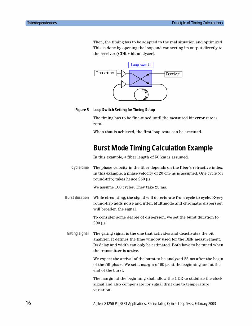
Then, the timing has to be adapted to the real situation and optimized. This is done by opening the loop and connecting its output directly to the receiver (CDR + bit analyzer).
Figure 5 Loop Switch Setting for Timing Setup
The timing has to be fine-tuned until the measured bit error rate is zero.
When that is achieved, the first loop tests can be executed.
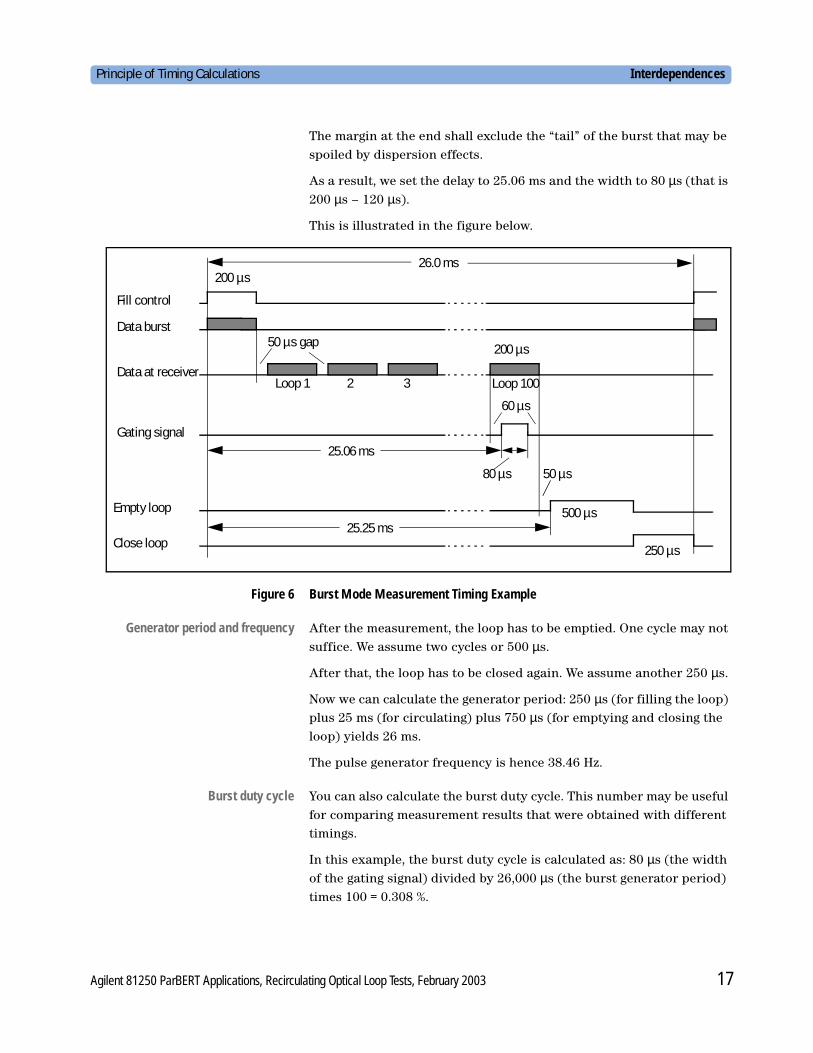
Burst Mode Timing Calculation ExampleIn this example, a fiber length of 50 km is assumed.
Cycle time The phase velocity in the fiber depends on the fiber’s refractive index. In this example, a phase velocity of 20 cm/ns is assumed. One cycle (or round-trip) takes hence 250 µs.
We assume 100 cycles. They take 25 ms.
Burst duration While circulating, the signal will deteriorate from cycle to cycle. Every round-trip adds noise and jitter. Multimode and chromatic dispersion will broaden the signal.
To consider some degree of dispersion, we set the burst duration to 200 µs.
Gating signal The gating signal is the one that activates and deactivates the bit analyzer. It defines the time window used for the BER measurement. Its delay and width can only be estimated. Both have to be tuned when the transmitter is active.
We expect the arrival of the burst to be analyzed 25 ms after the begin of the fill phase. We set a margin of 60 µs at the beginning and at the end of the burst.
The margin at the beginning shall allow the CDR to stabilize the clock signal and also compensate for signal drift due to temperature variation.
Transmitter Receiver
Loop switch
16 Agilent 81250 ParBERT Applications, Recirculating Optical Loop Tests, February 2003
Principle of Timing Calculations Interdependences
The margin at the end shall exclude the “tail” of the burst that may be spoiled by dispersion effects.
As a result, we set the delay to 25.06 ms and the width to 80 µs (that is 200 µs – 120 µs).
This is illustrated in the figure below.
Figure 6 Burst Mode Measurement Timing Example
Generator period and frequency After the measurement, the loop has to be emptied. One cycle may not suffice. We assume two cycles or 500 µs.
After that, the loop has to be closed again. We assume another 250 µs.
Now we can calculate the generator period: 250 µs (for filling the loop) plus 25 ms (for circulating) plus 750 µs (for emptying and closing the loop) yields 26 ms.
The pulse generator frequency is hence 38.46 Hz.
Burst duty cycle You can also calculate the burst duty cycle. This number may be useful for comparing measurement results that were obtained with different timings.
In this example, the burst duty cycle is calculated as: 80 µs (the width of the gating signal) divided by 26,000 µs (the burst generator period) times 100 = 0.308 %.
Fill control
Data burst
Data at receiverLoop 1 2 3 Loop 100
Gating signal
200 µs
50 µs gap
60 µs
25.06 ms
80 µs
200 µs
Empty loop
50 µs
500 µs
26.0 ms
Close loop250 µs
25.25 ms
Agilent 81250 ParBERT Applications, Recirculating Optical Loop Tests, February 2003 17
Interdependences Principle of Timing Calculations
NO TE You can see that these calculations are based on many assumptions. When you are setting up a recirculating loop test, you have to take the properties of the loop, the loop switch, the CDR, and the analyzer into account.
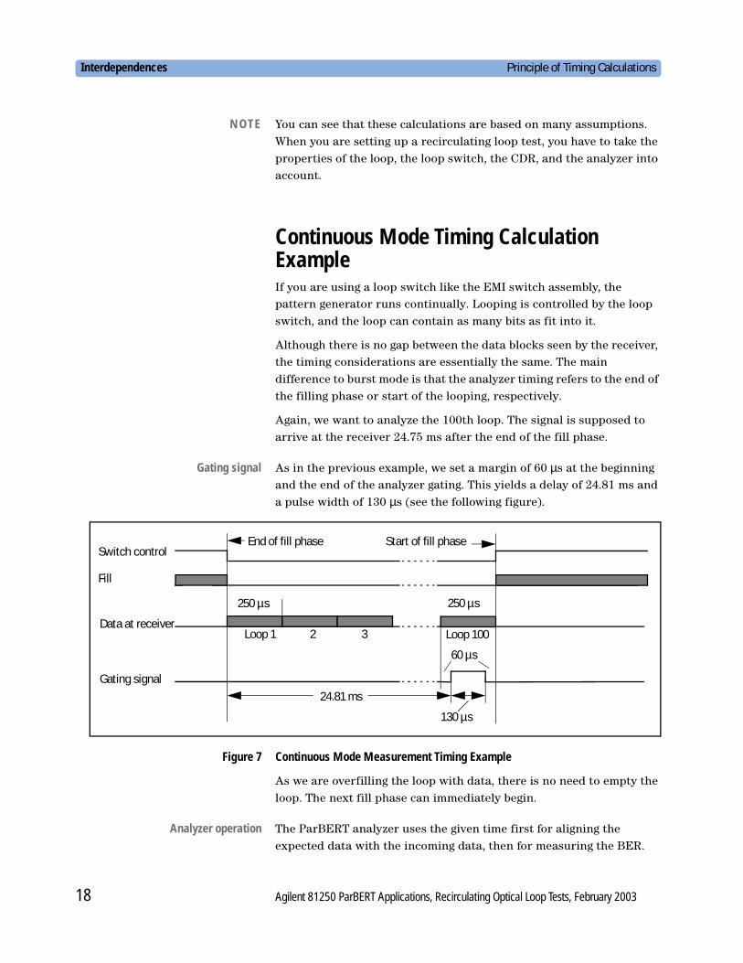
Continuous Mode Timing Calculation ExampleIf you are using a loop switch like the EMI switch assembly, the pattern generator runs continually. Looping is controlled by the loop switch, and the loop can contain as many bits as fit into it.
Although there is no gap between the data blocks seen by the receiver, the timing considerations are essentially the same. The main difference to burst mode is that the analyzer timing refers to the end of the filling phase or start of the looping, respectively.
Again, we want to analyze the 100th loop. The signal is supposed to arrive at the receiver 24.75 ms after the end of the fill phase.
Gating signal As in the previous example, we set a margin of 60 µs at the beginning and the end of the analyzer gating. This yields a delay of 24.81 ms and a pulse width of 130 µs (see the following figure).
Figure 7 Continuous Mode Measurement Timing Example
As we are overfilling the loop with data, there is no need to empty the loop. The next fill phase can immediately begin.
Analyzer operation The ParBERT analyzer uses the given time first for aligning the expected data with the incoming data, then for measuring the BER.
Switch control
Fill
Data at receiverLoop 1 2 3 Loop 100
Gating signal
250 µs
60 µs
24.81 ms
130 µs
250 µs
End of fill phase Start of fill phase
18 Agilent 81250 ParBERT Applications, Recirculating Optical Loop Tests, February 2003
Principle of Timing Calculations Interdependences
Fast Bit Synchronization is used (see also “Fast Bit Synchronization” on page 14). This requires only a minimum number of bits. For details please refer to the section Principles of Analyzer Sampling Point Adjustment in the ParBERT System User Guide.
Switching times You may wish to consider the speed of the loop switch. There is a delay between the electrical control signal and the opening or closing of the optical path, of course.
We have left that out in this example, because the delay of the EMI loop switch is below 0.1 µs.
ParBERT SpecialsThe two examples above have explained the principles of the timing calculation.
Actually, ParBERT analyzer systems are not controlled by a gating signal. The operation of a ParBERT system is controlled by the built-in sequencer.
Measurement duration The ParBERT sequence defines the duration of the measurement phase. The ParBERT user interface allows you to specify the length and number of repetitions of every sequence block. This in combination with the data rate is the way to set up the measurement duration.
External control of measurement If you wish to control the analyzer system like other data analyzers via an electrical signal, you can apply that signal to the trigger pod. The signal will then cause a sequence interrupt and a jump to the measurement block.
Due to inherent delays, the external signal has to be applied a well defined amount of time before the desired reaction (see also “Sequence for Pure Analyzer Operation” on page 34).
Remember: The measurement duration is specified in the sequence.
Test control via ParBERT If you use the ParBERT analyzer system for controlling the test phases, there is no gating signal at all. In this case, you set up a sequence that fulfills all the timing requirements (see also “Sequence for Test Control via ParBERT” on page 36).
Agilent 81250 ParBERT Applications, Recirculating Optical Loop Tests, February 2003 19
Interdependences Test Environment
Test Environment
The fiber-optic community is well aware that stable environment conditions often decide on the success or fiasco of a test. In addition, even polished fiber connectors are far from being foolproof. Some degree of expertise is required.
If the measured BER changes significantly while a test a running, this may be due to changes of the environment.
• Room temperature may rise during a long-term experiment. This can influence all components (for example, the timing setup and the decision thresholds).
You may have to operate ParBERT systems or other components at full fan speed.
• Even short-time changes of temperature and humidity can have an impact.
• Fibers react on changes of the geometry. It is essential that the mechanical setup is stable.
• Components (for example, optical modulators) may exhibit a drift with time.
NO TE When performing recirculating optical loop tests, environmental changes have to be observed and considered.
20 Agilent 81250 ParBERT Applications, Recirculating Optical Loop Tests, February 2003
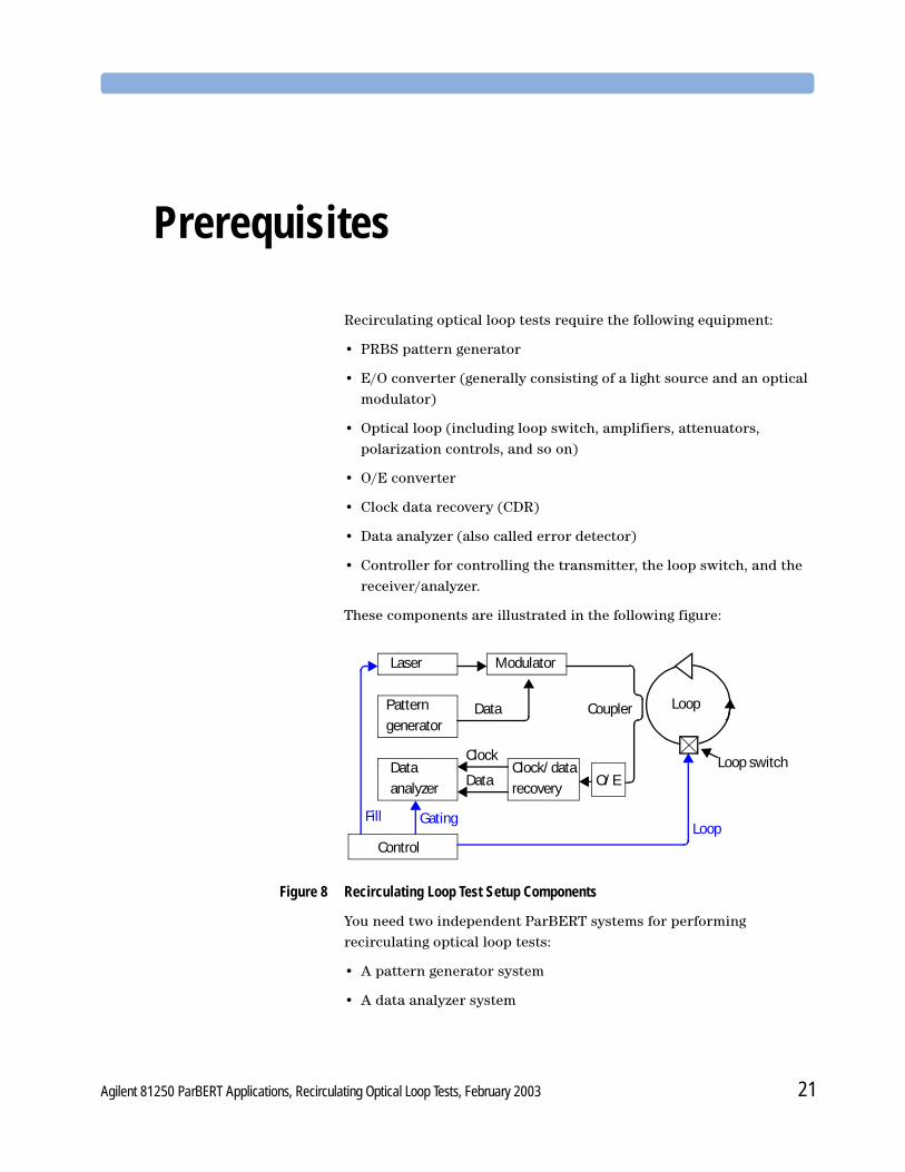
Prerequisites
Recirculating optical loop tests require the following equipment:
• PRBS pattern generator
• E/O converter (generally consisting of a light source and an optical modulator)
• Optical loop (including loop switch, amplifiers, attenuators, polarization controls, and so on)
• O/E converter
• Clock data recovery (CDR)
• Data analyzer (also called error detector)
• Controller for controlling the transmitter, the loop switch, and the receiver/analyzer.
These components are illustrated in the following figure:
Figure 8 Recirculating Loop Test Setup Components
You need two independent ParBERT systems for performing recirculating optical loop tests:
• A pattern generator system
• A data analyzer system
DataPattern
generator
Modulator
Data
analyzer
Control
Laser
Gating
Clock/data
recoveryData
Clock
LoopCoupler
Loop switchO/E
Fill Loop
Agilent 81250 ParBERT Applications, Recirculating Optical Loop Tests, February 2003 21
Prerequisites Configuration Examples with External Test Control
Two independent systems are needed, because clock frequency and phase at the receiving side have to be recovered from the incoming signal.
NO TE Electrical-to-optical and optical-to-electrical converters are required as well but will not be discussed in this manual. They must be able to handle the signal frequency.
Configuration Examples with External Test Control
The ParBERT system configuration to choose depends on your data rate requirements.
Data Rate Around 10 Gbit/s
Pattern generator For generating a data stream between 9.5 Gbit/s and 10.8 Gbit/s, you need one E4808A clock module and one E4866A 10.8 Gbit/s data generator module.
Please have a look at the technical specifications of the data generator module. You may wish to accelerate the rise and fall times of the generated pulses by adding an N4868A 10.8 Gbit/s Booster module.
Error detector For analyzing the received data, you need one E4808A clock module and one E4867A 10.8 Gbit/s data analyzer module.
22 Agilent 81250 ParBERT Applications, Recirculating Optical Loop Tests, February 2003
Configuration Examples with External Test Control Prerequisites
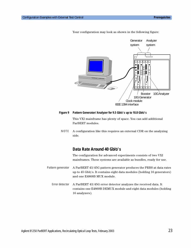
Your configuration may look as shown in the following figure:
Figure 9 Pattern Generator/Analyzer for 9.5 Gbit/s up to 10.8 Gbit/s
This VXI mainframe has plenty of space. You can add additional ParBERT modules.
NOTE A configuration like this requires an external CDR on the analyzing side.
Data Rate Around 40 Gbit/sThe configuration for advanced experiments consists of two VXI mainframes. These systems are available as bundles, ready for use.
Pattern generator A ParBERT 43/45G pattern generator produces the PRBS at data rates up to 45 Gbit/s. It contains eight data modules (holding 16 generators) and one E4868B MUX module.
Error detector A ParBERT 43/45G error detector analyzes the received data. It contains one E4869B DEMUX module and eight data modules (holding 16 analyzers).
IEEE 1394 interfaceClock module
10G GeneratorBooster 10G Analyzer
Generator
system
Analyzer
system
Agilent 81250 ParBERT Applications, Recirculating Optical Loop Tests, February 2003 23
Prerequisites Configuration Examples with External Test Control
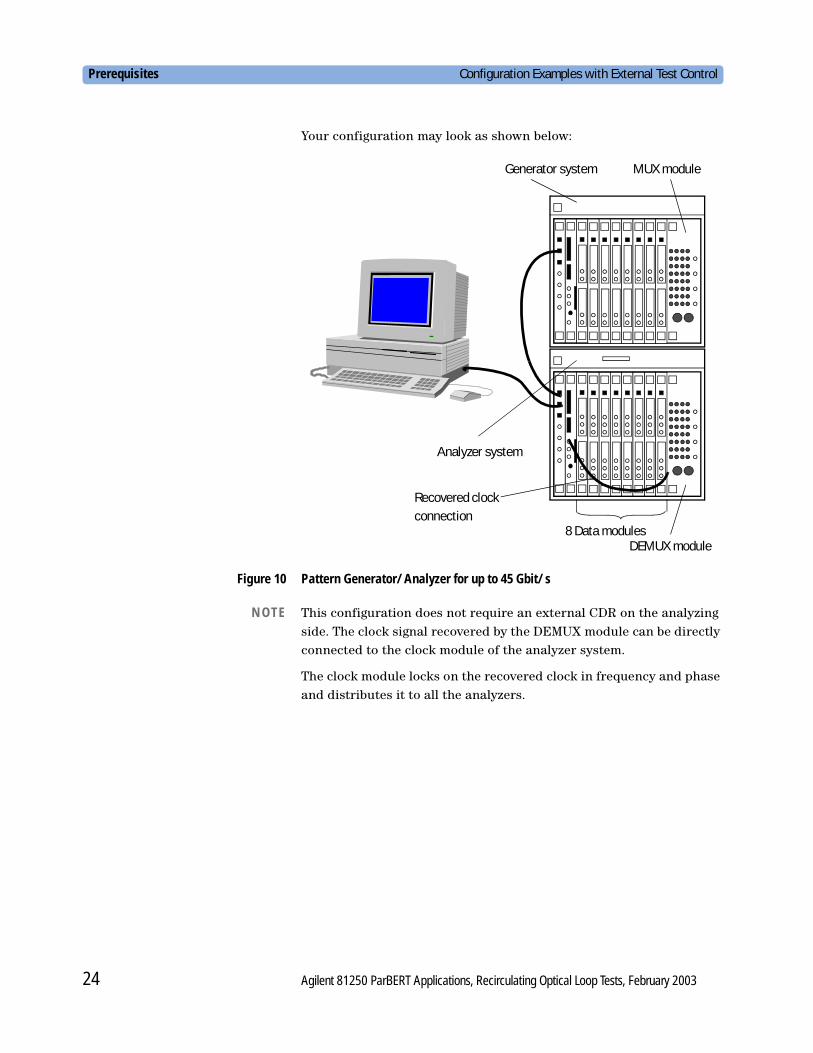
Your configuration may look as shown below:
Figure 10 Pattern Generator/Analyzer for up to 45 Gbit/s
NO TE This configuration does not require an external CDR on the analyzing side. The clock signal recovered by the DEMUX module can be directly connected to the clock module of the analyzer system.
The clock module locks on the recovered clock in frequency and phase and distributes it to all the analyzers.
8 Data modules
MUX module
DEMUX module
Generator system
Analyzer system
Recovered clock
connection
24 Agilent 81250 ParBERT Applications, Recirculating Optical Loop Tests, February 2003
Prerequisites for Test Control Prerequisites
Prerequisites for Test Control
You need to control the three or four phases of the experiment (see also “What are Recirculating Optical Loop Tests” on page 6):
• Fill phase
• Loop phase
• Analyzing phase
• Emptying phase
There are many ways to control the test. Much depends on the loop switch assembly you are using.
Test Control via External EquipmentFor example, a setup as illustrated in the figure “Recirculating Loop Test Setup Components” on page 21 would use an electrical pulse to control the fill phase by switching the light source on and off. It would use another pulse generator for controlling the loop switch and the analyzer.
You can use simple pulse generators. You can also use computer-controlled pulse generators. The pulse generators may be separate devices or custom boards built into the controlling computer.
Like any BERT, ParBERT systems can be controlled by electrical pulses. This is generally accomplished via the ParBERT trigger pod. However, inherent delays have to be considered.
On the other hand, you can also use your ParBERT analyzer system for controlling the test phases.
Test Control via ParBERT ModulesOne additional E4832A Data Generator/Analyzer Module (up to 675 MHz) can do the job. It can be equipped with up to four generator frontends. These frontends can generate the signals for controlling the loop switches.
Agilent 81250 ParBERT Applications, Recirculating Optical Loop Tests, February 2003 25
Prerequisites Configuration Examples with Internal Test Control
The advantages of this solution are:
• Easy synchronization of control signals
• The ParBERT user interface can be used for setting up and performing the test
• External pulse generators are not required
It depends on your frequency requirements whether the E4832A module can be simply added to the analyzer system or needs its own clock module.
You would have to add a clock module if the required frequencies for test control cannot be generated by multiplying or dividing the analyzer system frequency by factors of two.
Configuration Examples with Internal Test Control
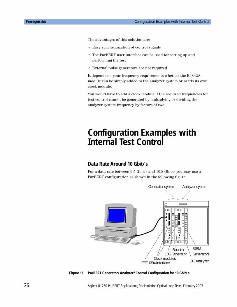
Data Rate Around 10 Gbit/sFor a data rate between 9.5 Gbit/s and 10.8 Gbit/s you may use a ParBERT configuration as shown in the following figure:
Figure 11 ParBERT Generator/Analyzer/Control Configuration for 10 Gbit/s
IEEE 1394 interfaceClock modules
10G GeneratorBooster
10G Analyzer
Generator system Analyzer system
675M
Generators
26 Agilent 81250 ParBERT Applications, Recirculating Optical Loop Tests, February 2003
Configuration Examples with Internal Test Control Prerequisites
The analyzer system would use the clock recovered by the external CDR. The data module for generating the control signals would use the analyzer clock.
Data Rate Around 40 Gbit/sA ParBERT 45G pattern generator or error detector requires a full VXI mainframe. These systems are still modular and can be expanded, but an additional mainframe is needed.
An expanded configuration may look as shown below:
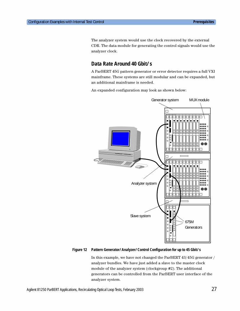
Figure 12 Pattern Generator/Analyzer/Control Configuration for up to 45 Gbit/s
In this example, we have not changed the ParBERT 43/45G generator / analyzer bundles. We have just added a slave to the master clock module of the analyzer system (clockgroup #2). The additional generators can be controlled from the ParBERT user interface of the analyzer system.
MUX moduleGenerator system
Analyzer system
Slave system
675M
Generators
Agilent 81250 ParBERT Applications, Recirculating Optical Loop Tests, February 2003 27
Prerequisites Configuration Examples with Internal Test Control
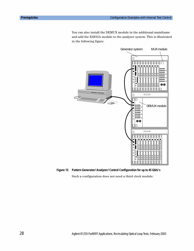
You can also install the DEMUX module in the additional mainframe and add the E4832A module to the analyzer system. This is illustrated in the following figure.
Figure 13 Pattern Generator/Analyzer/Control Configuration for up to 45 Gbit/s
Such a configuration does not need a third clock module.
MUX moduleGenerator system
DEMUX module
28 Agilent 81250 ParBERT Applications, Recirculating Optical Loop Tests, February 2003
Test Setup Procedures
This section provides an overview of the steps you have to carry out for setting up the ParBERT systems for a recirculating optical loop test.
More details are provided in “Setting up a 40 Gbit/s Optical Loop Test” on page 41.
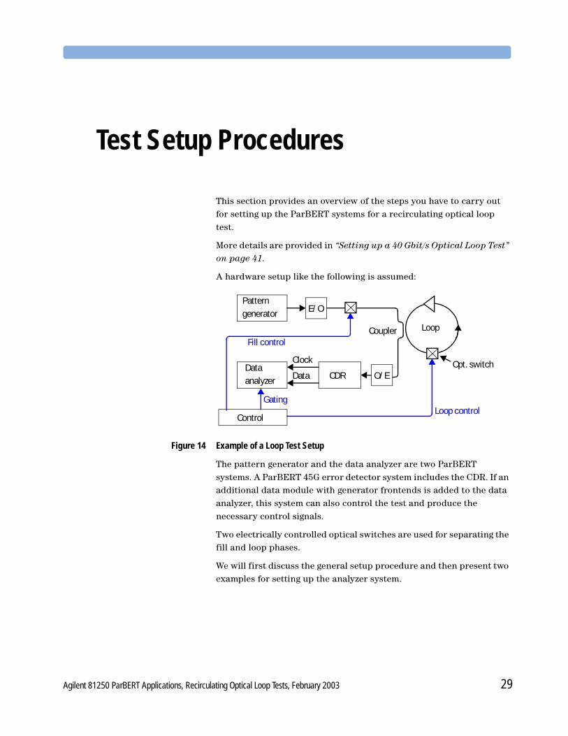
A hardware setup like the following is assumed:
Figure 14 Example of a Loop Test Setup
The pattern generator and the data analyzer are two ParBERT systems. A ParBERT 45G error detector system includes the CDR. If an additional data module with generator frontends is added to the data analyzer, this system can also control the test and produce the necessary control signals.
Two electrically controlled optical switches are used for separating the fill and loop phases.
We will first discuss the general setup procedure and then present two examples for setting up the analyzer system.
Pattern
generator
Data
analyzer
Control
Gating
CDRData
Clock
LoopCoupler
Opt. switchO/E
Loop control
E/O
Fill control
Agilent 81250 ParBERT Applications, Recirculating Optical Loop Tests, February 2003 29
Test Setup Procedures General Procedure
General Procedure
When setting up a recirculating optical loop experiment, one of the first goals is to determine the optimum analyzer sampling point. This point is characterized by a threshold level and a certain delay with respect to the analyzer clock.
The optimum analyzer threshold can most often be determined by means of an oscilloscope. Finding the optimum delay is usually not that simple.
The following general setup procedure is suggested:
1 Set up the transmitter.
That means:
– Prepare the pattern generator to generate a continuous pseudo random bit stream (PRBS). For ParBERT, a one-block sequence with an infinite loop is adequate.
– Set the levels and termination of the generated signal according to the characteristics of the E/O converter.
2 Start the transmitter.
Start the E/O converter and the pattern generator. An optical oscilloscope may be helpful to verify that a signal with high extinction ratio and low jitter is generated.
When that is achieved, keep the transmitter running. This ensures steady state conditions.
NO TE Remember that the CDR needs a continuous data stream for generating the analyzer source clock. Pure PRBS data is fine, because it has an equal probability of zeros and ones.
The CDR will tolerate and equalize PRBS discontinuities and minor gaps between bursts. It will have to resynchronize completely after a signal interrupt.
If that happens, the PLL of the analyzer system becomes unlocked—the analysis cannot be started.
3 Open the optical loop.
That means: Connect the transmitter to the CDR and the CDR outputs to the analyzer system.
– If you have a test setup as shown in “Example of a Loop Test Setup” on page 29, the loop is bypassed.
30 Agilent 81250 ParBERT Applications, Recirculating Optical Loop Tests, February 2003
General Procedure Test Setup Procedures
– If you have a loop switch like the EMI switch assembly, the signal passes once through the loop (see also the figure “Loop Switch Setting for Timing Setup” on page 16).
4 Check and connect the analyzer source clock.
Clock recovery is the task of the CDR.
You can use an external CDR. With ParBERT 43/45G systems, you can also use the CDR built into the E4869B DEMUX module of the error detector.
At a ParBERT 43/45G system, connect the Sys Clk Output of the DEMUX module to the CLOCK/REF INPUT of the clock module.
If you are using an external CDR, then:
– Inspect the recovered clock signal and adjust its levels.
– In case of a 10G system, connect the clock signal to the CLOCK/REF INPUT of the analyzer system.
– In case of a 43/45G system, connect the clock signal to Ext Clock Input of the DEMUX module.
5 Start and set up the analyzer system.
This involves the following:
– Set up the clock module to use the recovered (external) clock.
– In case of a 10G system, set up a data output port.
– Connect the analyzer input (= “DUT output”) signal physically and logically.
– Set the expected signal levels and data format.
6 Determine a suitable analyzer sampling delay.
This is done by measuring the BER with automatic sampling delay adjustment.
Remember that the optimum analyzer sampling delay depends on the bit rate of the signal. If you change the data rate, you have to repeat this step.
NOTE If you wish to exclude the optical equipment, you can determine and set the analyzer sampling delay also by connecting the generator output and analyzer input directly via the CDR. The CDR must not be bypassed.
– Ensure that the Measurement Configuration is set to Bit Error Rate (this is the default).
– Create a sequence that expects the generated PRBS. This can be done with the Standard Mode Sequence Editor.
Agilent 81250 ParBERT Applications, Recirculating Optical Loop Tests, February 2003 31
Test Setup Procedures General Procedure
– Enable Analyzer Synchronization and Automatic Bit Synchronization with Automatic Phase Alignment.
Auto Bit Sync with Auto Phase Alignment will report the necessary phase shift with respect to the clock.
– Run the test. The BER has to be zero.
– Open the Timing page of the Parameter Editor for the analyzer channel. It shows the present Start Delay (Periods + Time) and the Actual Delay. The difference between the two numbers is the required phase shift.
At a 10G system, enter this difference in the Time field.
At a 43/45G system, divide this difference by the channel period (which is 16 times the system period). Enter the result in the display field of the delay vernier.
NO TE In case of a 43/45G system, this adjustment has to be performed for all 16 analyzer channels.
– Change the sequence with the Detail Mode Sequence Editor. Remove the synchronization block and increase the block size.
TIP To measure a BER of 10–6, the block must hold more than one million bits.
– Enable Fast Bit Synchronization and repeat the BER measurement. The BER has to be zero.
7 Optimize the analyzer decision threshold.
This is done with the Parameter Editor while the BER measurement is running.
– At a 10G system, double click the DUT output port and open the Levels page. Move the Threshold voltage (only available in single-ended mode) stepwise in both directions until the BER increases. Set the Threshold voltage to the middle between the two extremes.
– At a 43/45G system, open the Input page of the Parameter Editor for the E4869B DEMUX module. Move the Threshold vernier stepwise in both directions until the BER increases. Position the vernier in the middle between the two extremes.
NO TE If you would use the 43/45G error detector with an external CDR, you would also have to tune the Sampling Phase.
32 Agilent 81250 ParBERT Applications, Recirculating Optical Loop Tests, February 2003
Analyzer System Setup Test Setup Procedures
8 Save the analyzer system setting.
The automatic sampling delay adjustment has found the optimum sampling point for the undistorted signal. This setting forms the basis for the following loop tests.
TIP The present setting of the sampling delay(s) refers to a certain bit rate. If you plan to experiment with the bit rate, it might be a good idea to state that rate in the setting name.
9 Prepare the analyzer system for the loop test.
That means basically:
– Consider the analyzer gating.
– Set up a suitable sequence.
– Enable Fast Bit Synchronization.
The following section provides two setup examples.
Analyzer System Setup
The operation of a ParBERT system is defined by a sequence. This refers to generator and analyzer systems.
A sequence consists of blocks that are executed once or repeatedly. They specify generated and/or expected data. The sequence flow can be controlled by electrical pulses (for example, applied to the trigger pod) or by a program.
With the Detail Mode Sequence Editor of the ParBERT user interface, you can set up single or repeated BER measurements without any programming effort. The ParBERT user interface reports the updated results. This is convenient for setting up the test.
When it comes to automated tests, you will have to control the sequence flow by means of a program. This program would check the success of the Fast Bit Synchronization (see also “Alignment of Received and Expected Data” on page 14). It would discard all measurements that obviously failed, accumulate only the plausible results, and restart the test.
We differentiate between pure analyzer systems and analyzer systems that are also used for controlling the test.
Agilent 81250 ParBERT Applications, Recirculating Optical Loop Tests, February 2003 33
Test Setup Procedures Analyzer System Setup
Sequence for Pure Analyzer OperationThe sequence flow of ParBERT systems can be controlled via so-called events. The trigger pod can cause an event. The trigger pod has eight TTL inputs. Every input (changing from low to high or vice versa) can cause a specific action.
Events can also be caused by other sources or by software commands—please refer to the ParBERT System User Guide and the ParBERT Programming Guide and SCPI Reference.
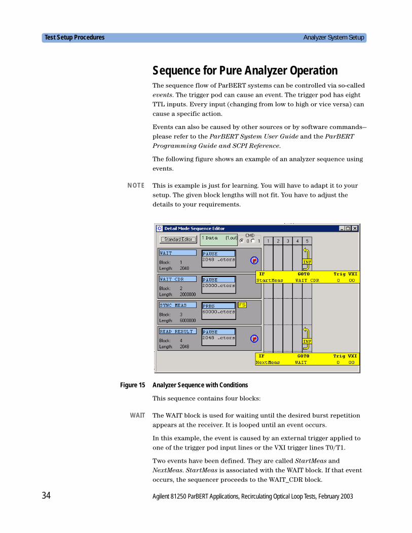
The following figure shows an example of an analyzer sequence using events.
NO TE This is example is just for learning. You will have to adapt it to your setup. The given block lengths will not fit. You have to adjust the details to your requirements.
Figure 15 Analyzer Sequence with Conditions
This sequence contains four blocks:
WAIT The WAIT block is used for waiting until the desired burst repetition appears at the receiver. It is looped until an event occurs.
In this example, the event is caused by an external trigger applied to one of the trigger pod input lines or the VXI trigger lines T0/T1.
Two events have been defined. They are called StartMeas and NextMeas. StartMeas is associated with the WAIT block. If that event occurs, the sequencer proceeds to the WAIT_CDR block.
34 Agilent 81250 ParBERT Applications, Recirculating Optical Loop Tests, February 2003
Analyzer System Setup Test Setup Procedures
NOTE It is the responsibility of the timing control to place the event correctly. Inherent delays have to be considered.
For example, it takes 36 periods of the internal sequencer clock until the sequencer starts executing the designated block. The sequencer clock period is calculated as
Clkp _period = system clock period × segment resolution
For details, please refer to the section How to Specify Events and Reactions Upon Events of the ParBERT System User Guide.
WAIT_CDR The WAIT_CDR block is used for allowing the CDR to settle. This is necessary, because the data at the beginning of a burst is most often not the continuation of the last burst. Data and signal discontinuity causes a phase shift that the CDR has to compensate for. The minimum required time depends on the CDR circuit.
In this example, the WAIT_CDR block is executed once. Its length depends on the data rate. In the figure above, it has a length of 2 million vectors. At a data rate of 40 Gbit/s, this corresponds to a wait time of 50 µs.
SYNC_MEAS This block is used for both Fast Bit Synchronization and the BER measurement. The expected data is the generated PRBS. The FS symbol indicates that Fast Bit Synchronization has been enabled.
The SYNC_MEAS block is executed once. Its length determines the duration of the burst analysis.
In the figure above, it has a length of 6 million vectors. At a data rate of 40 Gbit/s, this corresponds to an analysis time of 150 µs.
NOTE Please remember the “Burst Mode Timing Calculation Example” on page 16. We do not want to analyze the tail of the burst. The accumulated times of the WAIT_CDR block and the SYNC_MEAS block have to be less than the signal travelling time through the loop.
Assuming a 50 km loop with a travelling time of about 250 µs, this example meets the requirement.
READ_RESULT The READ_RESULT block allows the controlling program to read the BER counters, reject questionable results, accumulate probable results, and reset the BER counters.
Resetting the BER counters is necessary, because the analyzer system cannot check the success or failure of the Fast Bit Synchronization. It would accumulate all results.
Agilent 81250 ParBERT Applications, Recirculating Optical Loop Tests, February 2003 35
Test Setup Procedures Analyzer System Setup
When that is done, the controlling program can generate an event for repeating the test. The event NextMeas is associated with the READ_RESULT block.
When that event occurs, the sequencer returns to the WAIT block.
RemarksIn principle, the StartMeas event could also be caused by a software command that changes CMD0 to CMD1.
This, however, is only useful, if the ParBERT analyzer system also controls the loop switches. If the switches are controlled by external pulses, as in this example, the measurement start must also be controlled by an external pulse.
Sequence for Test Control via ParBERTHere, we use an additional ParBERT module for providing the control signals.
One DUT output and two DUT input ports have been set up. The input ports are connected to two generator frontends that control the fill and loop phases of the test.
In this example, the following is assumed:
• The fill phase lasts as long as the Fill control signal is high.
• The loop is closed when the Loop control signal becomes high. It is opened when the Loop control signal becomes low.
Complementary operation of the two signals ensures that the CDR always receives data and does not get unlocked.
NO TE Ensure that the loop switches are never in fill and loop state at the same time. Otherwise, the receiver would get a superimposed signal and the CDR would randomly lock and unlock.
36 Agilent 81250 ParBERT Applications, Recirculating Optical Loop Tests, February 2003
Analyzer System Setup Test Setup Procedures
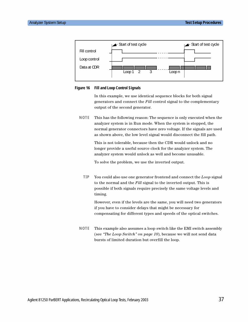
Figure 16 Fill and Loop Control Signals
In this example, we use identical sequence blocks for both signal generators and connect the Fill control signal to the complementary output of the second generator.
NOTE This has the following reason: The sequence is only executed when the analyzer system is in Run mode. When the system is stopped, the normal generator connectors have zero voltage. If the signals are used as shown above, the low level signal would disconnect the fill path.
This is not tolerable, because then the CDR would unlock and no longer provide a useful source clock for the analyzer system. The analyzer system would unlock as well and become unusable.
To solve the problem, we use the inverted output.
TIP You could also use one generator frontend and connect the Loop signal to the normal and the Fill signal to the inverted output. This is possible if both signals require precisely the same voltage levels and timing.
However, even if the levels are the same, you will need two generators if you have to consider delays that might be necessary for compensating for different types and speeds of the optical switches.
NOTE This example also assumes a loop switch like the EMI switch assembly (see “The Loop Switch” on page 10), because we will not send data bursts of limited duration but overfill the loop.
Fill control
Loop control
Data at CDRLoop 1 2 3 Loop n
Start of test cycle Start of test cycle
Agilent 81250 ParBERT Applications, Recirculating Optical Loop Tests, February 2003 37
Test Setup Procedures Analyzer System Setup
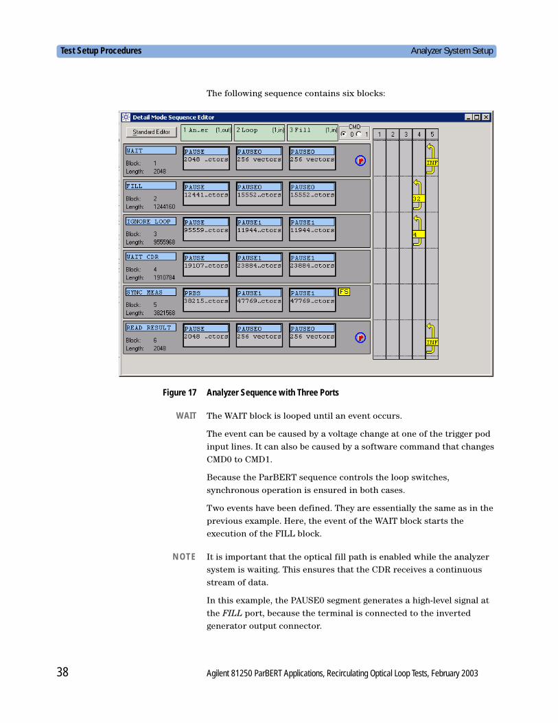
The following sequence contains six blocks:
Figure 17 Analyzer Sequence with Three Ports
WAIT The WAIT block is looped until an event occurs.
The event can be caused by a voltage change at one of the trigger pod input lines. It can also be caused by a software command that changes CMD0 to CMD1.
Because the ParBERT sequence controls the loop switches, synchronous operation is ensured in both cases.
Two events have been defined. They are essentially the same as in the previous example. Here, the event of the WAIT block starts the execution of the FILL block.
NO TE It is important that the optical fill path is enabled while the analyzer system is waiting. This ensures that the CDR receives a continuous stream of data.
In this example, the PAUSE0 segment generates a high-level signal at the FILL port, because the terminal is connected to the inverted generator output connector.
38 Agilent 81250 ParBERT Applications, Recirculating Optical Loop Tests, February 2003
Analyzer System Setup Test Setup Procedures
FILL The FILL block has a length of 1,244,160 vectors. It is repeated 32 times. At a data rate of 40 Gbit/s, this takes 1 ms.
Assuming a 50 km loop with a travelling time of about 250 µs, we fill the loop four times. This allows amplifiers, rectifiers, polarization controls, and other optical-electrical loop components to reach a steady state.
IGNORE_LOOP In this block, we disconnect the pattern generator, close the loop, and wait for the nth signal repetition.
To adjust the wait time as precisely as possible, you need detailed information about the loop characteristics.
In this example, a signal travelling time of 240 µs (240,000 ns) was measured. At a data rate of 40 Gbit/s (0.025 ns per bit), this loop holds 9.6 million bits.
The block length has been set to 9,555,968 vectors.
NOTE The minimum step size for increasing or decreasing the block length is given by the general segment resolution of the ParBERT system. Here, a segment resolution of 2048 bits is used.
In this example, the IGNORE_LOOP block is four times repeated. We ignore four repetitions. The fifth signal repetition is the one we want to analyze.
NOTE In burst mode, your timing has to match the signal travelling time very precisely in order to address the nth repetition exactly. The above setting would not be precise enough for analyzing the 100th signal repetition. You may wish to tune the signal frequency to cover with the block length restrictions.
Because we are using continuous mode in this example, the timing can be more relaxed. We have filled the loop completely. It is therefore not that important whether we start the analysis a little bit sooner or later.
WAIT_CDR This block has the same function as in the previous example. It allows the CDR to stabilize the recovered clock.
The WAIT_CDR block has a length of 1,910,784 vectors. At a data rate of 40 Gbit/s, this corresponds to 47.77 µs.
SYNC_MEAS This block is used for both Fast Bit Synchronization and the BER measurement. The expected data is the generated PRxS. The FS symbol indicates that Fast Bit Synchronization has been enabled.
Agilent 81250 ParBERT Applications, Recirculating Optical Loop Tests, February 2003 39
Test Setup Procedures Analyzer System Setup
The SYNC_MEAS block is executed once. Its length determines the duration of the analysis.
In the figure above, it has a length of 3,821,568 vectors. At a data rate of 40 Gbit/s, this corresponds to an analysis time of 95.54 µs. The remainder of the “burst” (96.69 µs) is discarded.
READ_RESULT The READ_RESULT block opens the loop, connects the pattern generator (a must for continuous operation of the CDR), and allows the controlling program to read the BER counters, reject questionable results, accumulate probable results, and reset the BER counters.
When that is done, the controlling program can generate a CMD0 event for repeating the test.
When that event occurs, the sequencer returns to the WAIT block.
RemarksIt depends on the loop switch whether an additional emptying phase is required. This example refers to continuous mode where the loop is overfilled and does not have to be emptied.
40 Agilent 81250 ParBERT Applications, Recirculating Optical Loop Tests, February 2003
Setting up a 40 Gbit/s Optical Loop Test
This example refers to a recirculating optical loop experiment performed at the COM - Education & Research Center of the Technical University of Denmark.
The EMI loop switch was used (see also “The Loop Switch” on page 10). It could be demonstrated that high speed ParBERT systems can be used for this kind of test.
NOTE This is just one example. Different setups and especially different loop switches require different solutions.
In addition, this example is not program-controlled. Long-term tests would require a program that differentiates between good and poor results of the Fast Bit Synchronization and accumulates only plausible results.
On the other hand, ParBERT shows also instantaneous results, updated every second. By observing these results, one should be able to adjust and optimize the electro-optical setup.
Please continue with:
• “Focus of this Example” on page 42
• “Hardware Setup” on page 43
• “Pattern Generator Setup” on page 45
• “Pattern Analyzer Setup” on page 50
• “Running the Test” on page 65
• “Concluding Remarks” on page 66
Agilent 81250 ParBERT Applications, Recirculating Optical Loop Tests, February 2003 41
Setting up a 40 Gbit/s Optical Loop Test Focus of this Example
Focus of this Example
This example uses two ParBERT systems.
• We use one ParBERT 43 Gbit/s pattern generator system and a 40G E/O converter that generates the serial data stream for filling the loop.
• We use a 40G O/E converter and a ParBERT 43 Gbit/s error detector system that analyzes the nth loop cycle.
• The loop consists of 50 km optical fiber, amplifier, attenuator, optical couplers, and polarization controls.
• Pure, undistorted PRWS data is generated and expected.
• The test phases are controlled by a low-speed E4832A data module with four data generator frontends.
• The sampling delay of the analyzers is manually set.
• The bit error rate (BER) is measured.
What you will learn You will learn:
• How to set up the pattern generator system
• How to create the stimulating pattern
• How to set up the analyzer system
• How to set up the analyzer test sequence
42 Agilent 81250 ParBERT Applications, Recirculating Optical Loop Tests, February 2003
Hardware Setup Setting up a 40 Gbit/s Optical Loop Test
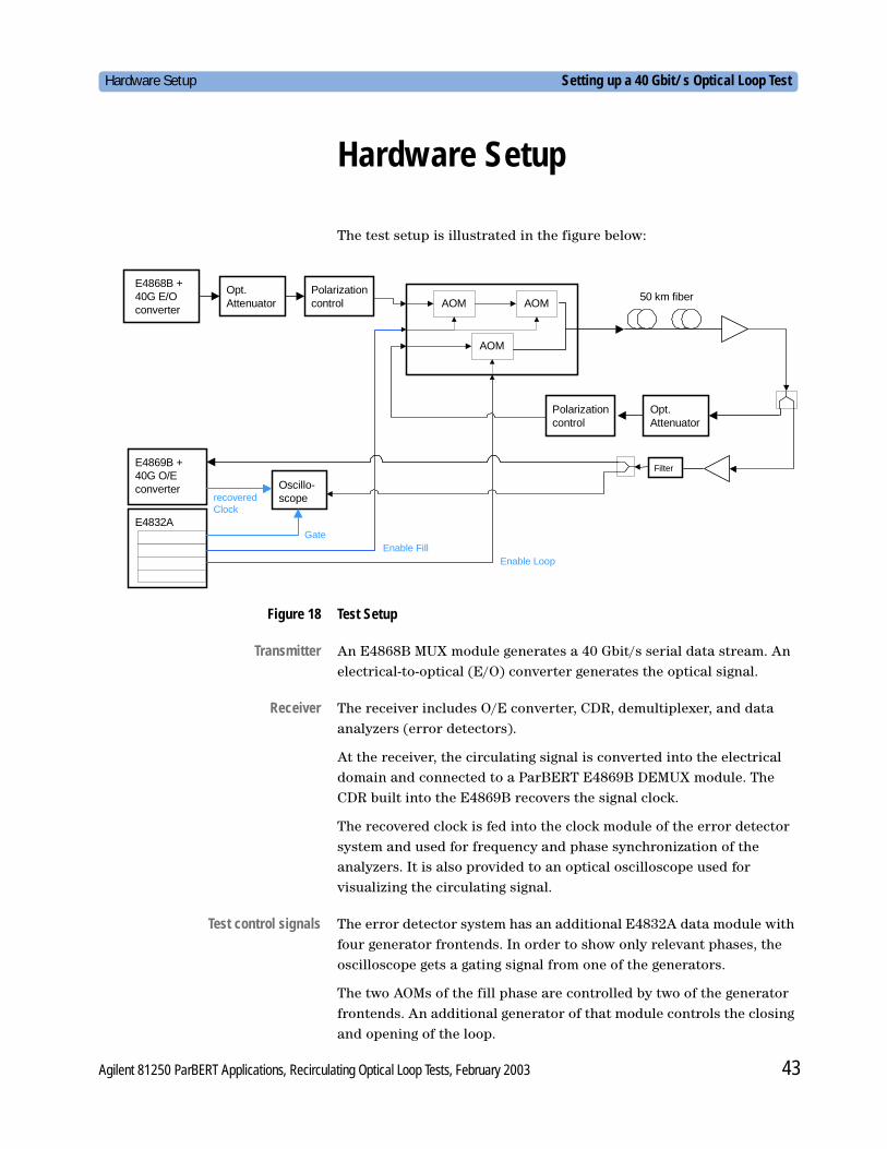
Hardware Setup
The test setup is illustrated in the figure below:
Figure 18 Test Setup
Transmitter An E4868B MUX module generates a 40 Gbit/s serial data stream. An electrical-to-optical (E/O) converter generates the optical signal.
Receiver The receiver includes O/E converter, CDR, demultiplexer, and data analyzers (error detectors).
At the receiver, the circulating signal is converted into the electrical domain and connected to a ParBERT E4869B DEMUX module. The CDR built into the E4869B recovers the signal clock.
The recovered clock is fed into the clock module of the error detector system and used for frequency and phase synchronization of the analyzers. It is also provided to an optical oscilloscope used for visualizing the circulating signal.
Test control signals The error detector system has an additional E4832A data module with four generator frontends. In order to show only relevant phases, the oscilloscope gets a gating signal from one of the generators.
The two AOMs of the fill phase are controlled by two of the generator frontends. An additional generator of that module controls the closing and opening of the loop.
E4868B +40G E/Oconverter
E4832A
E4869B +40G O/Econverter
AOM AOM
AOM
Opt.Attenuator
Filter
Oscillo-scope
Gate
recoveredClock
Enable FillEnable Loop
50 km fiberPolarizationcontrol
Polarizationcontrol
Opt.Attenuator
Agilent 81250 ParBERT Applications, Recirculating Optical Loop Tests, February 2003 43
Setting up a 40 Gbit/s Optical Loop Test Hardware Setup
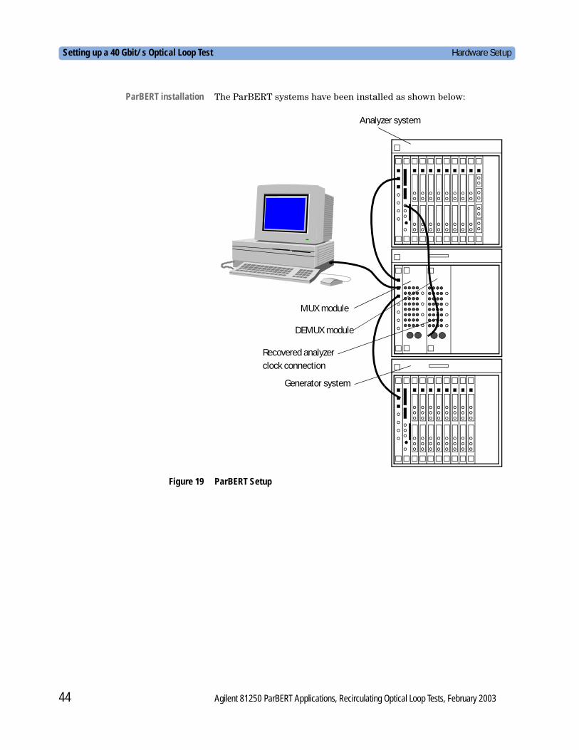
ParBERT installation The ParBERT systems have been installed as shown below:
Figure 19 ParBERT Setup
MUX module
Analyzer system
DEMUX module
Generator system
Recovered analyzer
clock connection
44 Agilent 81250 ParBERT Applications, Recirculating Optical Loop Tests, February 2003
Pattern Generator Setup Setting up a 40 Gbit/s Optical Loop Test
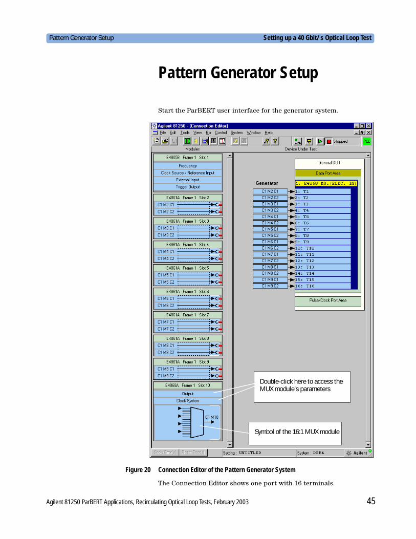
Pattern Generator Setup
Start the ParBERT user interface for the generator system.
Figure 20 Connection Editor of the Pattern Generator System
The Connection Editor shows one port with 16 terminals.
Double-click here to access the MUX module’s parameters
Symbol of the 16:1 MUX module
Agilent 81250 ParBERT Applications, Recirculating Optical Loop Tests, February 2003 45
Setting up a 40 Gbit/s Optical Loop Test Pattern Generator Setup
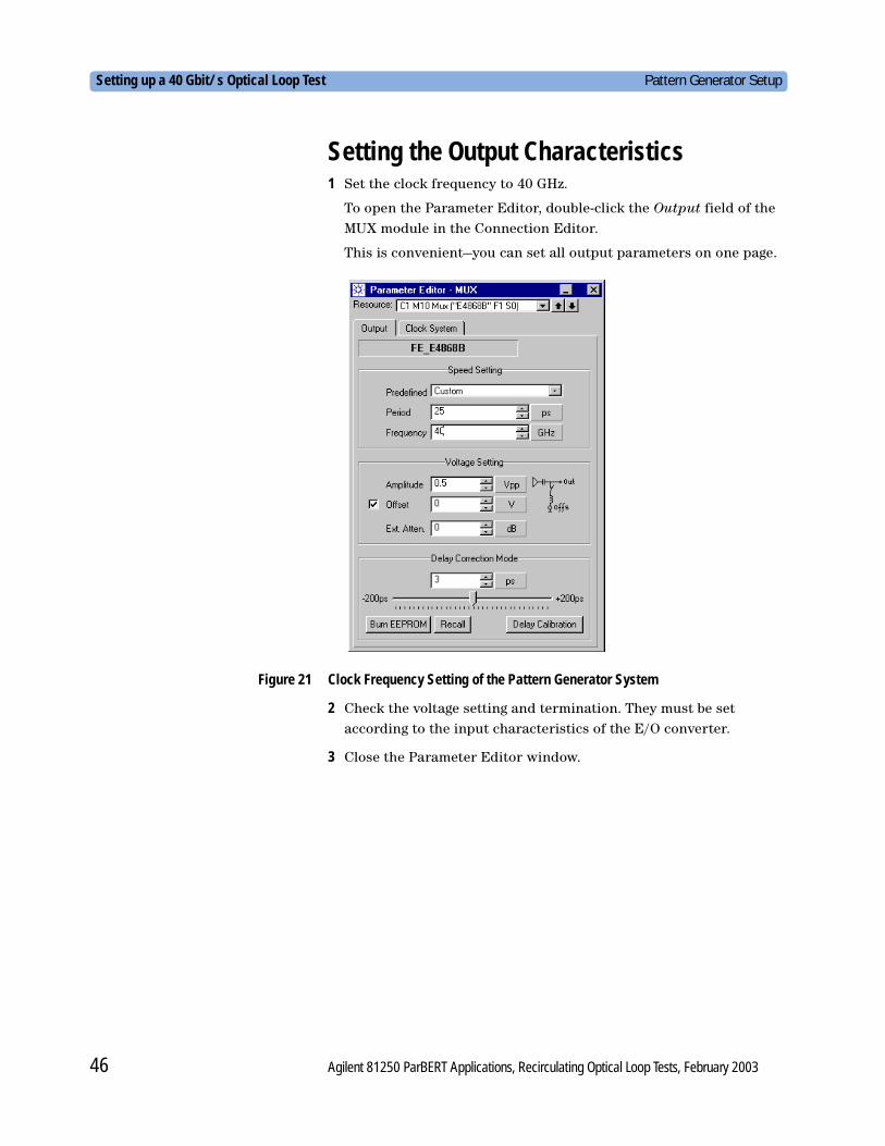
Setting the Output Characteristics1 Set the clock frequency to 40 GHz.
To open the Parameter Editor, double-click the Output field of the MUX module in the Connection Editor.
This is convenient—you can set all output parameters on one page.
Figure 21 Clock Frequency Setting of the Pattern Generator System
2 Check the voltage setting and termination. They must be set according to the input characteristics of the E/O converter.
3 Close the Parameter Editor window.
46 Agilent 81250 ParBERT Applications, Recirculating Optical Loop Tests, February 2003
Pattern Generator Setup Setting up a 40 Gbit/s Optical Loop Test
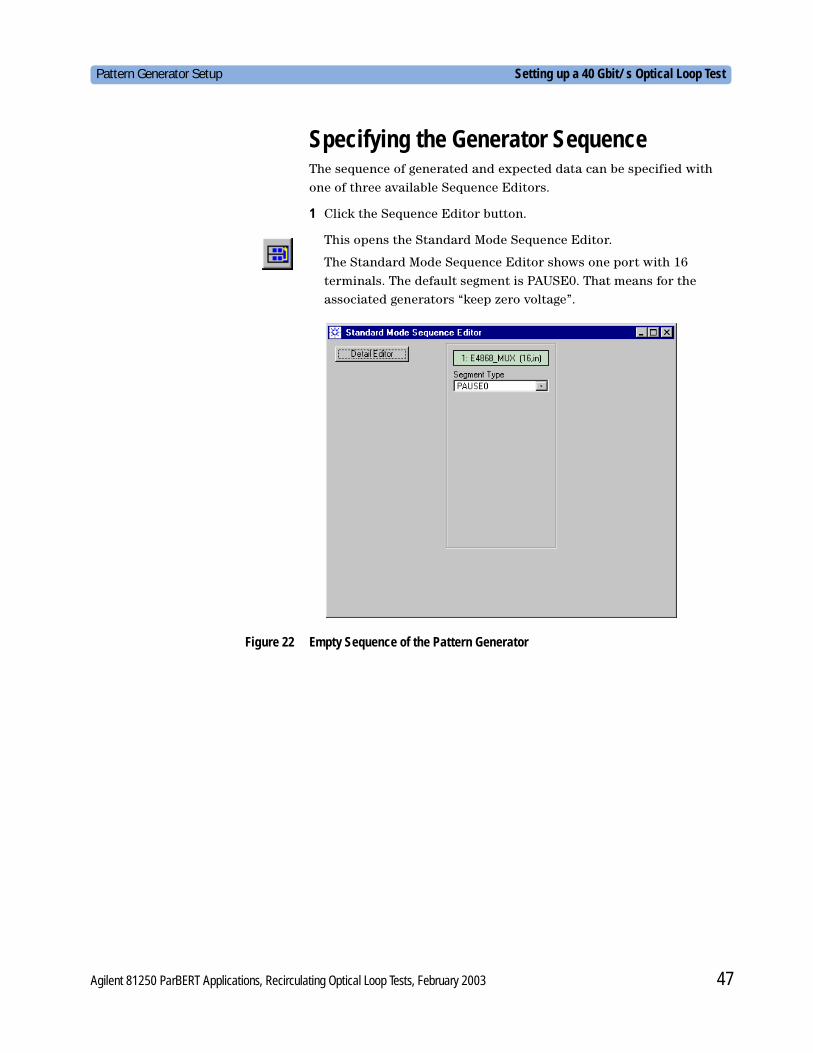
Specifying the Generator SequenceThe sequence of generated and expected data can be specified with one of three available Sequence Editors.
1 Click the Sequence Editor button.
This opens the Standard Mode Sequence Editor.
The Standard Mode Sequence Editor shows one port with 16 terminals. The default segment is PAUSE0. That means for the associated generators “keep zero voltage”.
Figure 22 Empty Sequence of the Pattern Generator
Agilent 81250 ParBERT Applications, Recirculating Optical Loop Tests, February 2003 47
Setting up a 40 Gbit/s Optical Loop Test Pattern Generator Setup
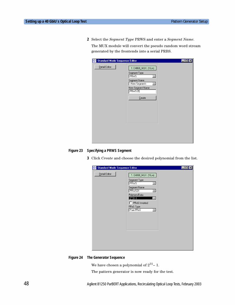
2 Select the Segment Type PRWS and enter a Segment Name.
The MUX module will convert the pseudo random word stream generated by the frontends into a serial PRBS.
Figure 23 Specifying a PRWS Segment
3 Click Create and choose the desired polynomial from the list.
Figure 24 The Generator Sequence
We have chosen a polynomial of 231– 1.
The pattern generator is now ready for the test.
48 Agilent 81250 ParBERT Applications, Recirculating Optical Loop Tests, February 2003
Pattern Generator Setup Setting up a 40 Gbit/s Optical Loop Test
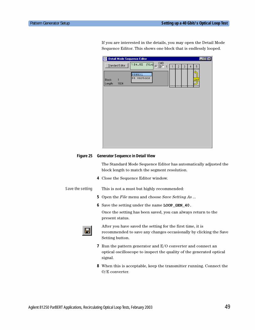
If you are interested in the details, you may open the Detail Mode Sequence Editor. This shows one block that is endlessly looped.
Figure 25 Generator Sequence in Detail View
The Standard Mode Sequence Editor has automatically adjusted the block length to match the segment resolution.
4 Close the Sequence Editor window.
Save the setting This is not a must but highly recommended:
5 Open the File menu and choose Save Setting As ...
6 Save the setting under the name LOOP_GEN_40.
Once the setting has been saved, you can always return to the present status.
After you have saved the setting for the first time, it is recommended to save any changes occasionally by clicking the Save Setting button.
7 Run the pattern generator and E/O converter and connect an optical oscilloscope to inspect the quality of the generated optical signal.
8 When this is acceptable, keep the transmitter running. Connect the O/E converter.
Agilent 81250 ParBERT Applications, Recirculating Optical Loop Tests, February 2003 49
Setting up a 40 Gbit/s Optical Loop Test Pattern Analyzer Setup
NO TE If you were using an external CDR, you would now connect the CDR and check the quality of the recovered clock signal. You would also adjust the clock levels to the sensitivity of the analyzer system’s CLOCK/REF INPUT.
In this example, we use the CDR built into the E4869B DEMUX module. Therefore, we need only set up the analyzer system.
Pattern Analyzer Setup
This example requires two ParBERT systems and hence two ParBERT user interfaces.
After starting the user interface of the analyzer system, the Connection Editor appears. The 16 analyzers are automatically connected to the DEMUX module.
We have set up three additional DUT input ports.
• The FillCtrl port has two terminals for controlling both switches of the fill path.
• The LoopCtrl port has one terminal for controlling the loop switch.
• The Data port has one terminal for gating the optical oscilloscope during the measurement phase.
50 Agilent 81250 ParBERT Applications, Recirculating Optical Loop Tests, February 2003
Pattern Analyzer Setup Setting up a 40 Gbit/s Optical Loop Test
The connections are shown in the figure below:
Figure 26 Connection Editor of the Analyzer System
You will now:
• Set up the analyzer system clock (see “Setting Up the Analyzer System Clock” on page 52)
• Specify the analyzer timing (see “Setting the Analyzer Sampling Delays” on page 54)
• Define the test sequence (see “Specifying the Analyzer Test Sequence” on page 63)
TIP Please keep in mind that at least the generators of the analyzer system require a cable and propagation delay compensation. This is a general requirement for every new test setup and is done with the Deskew Editor.
Agilent 81250 ParBERT Applications, Recirculating Optical Loop Tests, February 2003 51
Setting up a 40 Gbit/s Optical Loop Test Pattern Analyzer Setup
The procedure is described in the section “How to Compensate for Internal and External Delays“ of the ParBERT System User Guide. It will not be discussed in this example.
Setting Up the Analyzer System ClockThe test setup shown in the figure “Hardware Setup” on page 43 requires that the generator system is running. The loop is open and the transmitted signal is connected to the E4869B DEMUX module.
1 Connect the Sys Clk Output of the DEMUX module to the CLOCK/REF INPUT of the analyzer system’s clock module.
The DEMUX module provides a clock signal that is 1/16th of its own clock.
2 Ensure that the DEMUX module is in Internal (CDR) mode.
This is done by double-clicking the Clock System field in the Connection Editor.
Figure 27 Clock System Page of the Parameter Editor
3 Ensure that CLOCK/REF INPUT is enabled and the Clock Multiplier is set to 16. These are the defaults for Internal (CDR) mode.
The corresponding window is accessed by double-clicking the Clock Source / Reference Input field in the Connection Editor.
52 Agilent 81250 ParBERT Applications, Recirculating Optical Loop Tests, February 2003
Pattern Analyzer Setup Setting up a 40 Gbit/s Optical Loop Test
4 Enter the expected clock frequency.
Figure 28 Clock System Page of the Parameter Editor
5 Make sure that the PLL symbol of the analyzer user interface has turned to green.
6 Close the Parameter Editor window.
TIP From now on, do not stop the run of the generator system. During setup, the pattern generator system continually feeds the CDR, which in turn generates the clock signal onto which the analyzer system has locked.
If you would stop the generator system, the green PLL indicator at the upper right-hand corner of the analyzer system would turn red.
The letters CDR indicate that the phase locked loop of the CDR has lost its clock synchronization. In order to re-synchronize, you would have to repeat the procedure described in this section.
Save the setting This is a good moment for saving the analyzer setting.
7 Use File – Save Setting as ... to save the setting under the name LOOP_ANA_40.
Once the setting has been saved, you can always return to the present status.
Agilent 81250 ParBERT Applications, Recirculating Optical Loop Tests, February 2003 53
Setting up a 40 Gbit/s Optical Loop Test Pattern Analyzer Setup
Setting the Analyzer Sampling DelaysTo determine the optimum sampling point, we will execute a simple BER measurement with Automatic Bit Synchronization.
NO TE In this example, we do that with all the optical equipment like switches, E/O, loop components, and O/E converters involved. This gives us confidence that the whole optical setup is working.
If you wish to exclude the optical equipment, you can determine and set the analyzer sampling delay also by connecting the generator output and analyzer input directly via the CDR. Note that the CDR, external or internal, must not be bypassed.
1 Make sure that the Bit Error Rate Measurement is enabled. This is the default.
Figure 29 Measurement Configuration
54 Agilent 81250 ParBERT Applications, Recirculating Optical Loop Tests, February 2003
Pattern Analyzer Setup Setting up a 40 Gbit/s Optical Loop Test
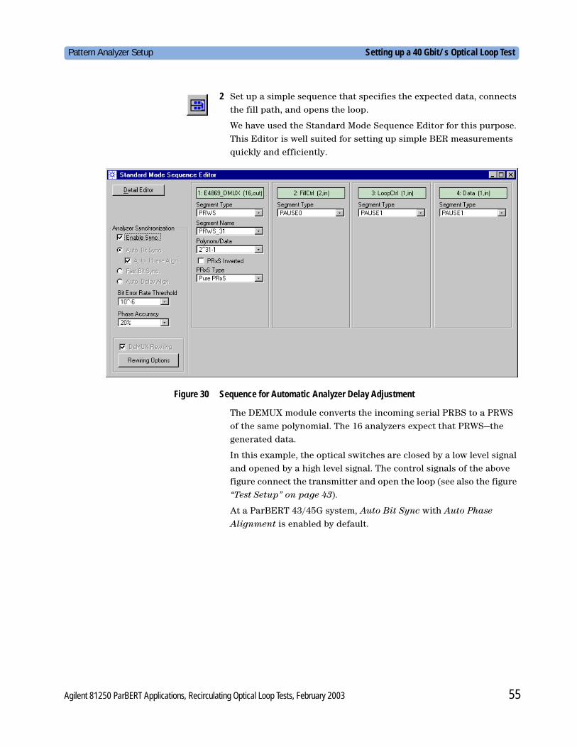
2 Set up a simple sequence that specifies the expected data, connects the fill path, and opens the loop.
We have used the Standard Mode Sequence Editor for this purpose. This Editor is well suited for setting up simple BER measurements quickly and efficiently.
Figure 30 Sequence for Automatic Analyzer Delay Adjustment
The DEMUX module converts the incoming serial PRBS to a PRWS of the same polynomial. The 16 analyzers expect that PRWS—the generated data.
In this example, the optical switches are closed by a low level signal and opened by a high level signal. The control signals of the above figure connect the transmitter and open the loop (see also the figure “Test Setup” on page 43).
At a ParBERT 43/45G system, Auto Bit Sync with Auto Phase Alignment is enabled by default.
Agilent 81250 ParBERT Applications, Recirculating Optical Loop Tests, February 2003 55
Setting up a 40 Gbit/s Optical Loop Test Pattern Analyzer Setup
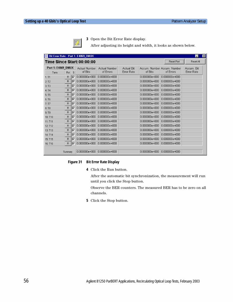
3 Open the Bit Error Rate display.
After adjusting its height and width, it looks as shown below.
Figure 31 Bit Error Rate Display
4 Click the Run button.
After the automatic bit synchronization, the measurement will run until you click the Stop button.
Observe the BER counters. The measured BER has to be zero on all channels.
5 Click the Stop button.
56 Agilent 81250 ParBERT Applications, Recirculating Optical Loop Tests, February 2003
Pattern Analyzer Setup Setting up a 40 Gbit/s Optical Loop Test
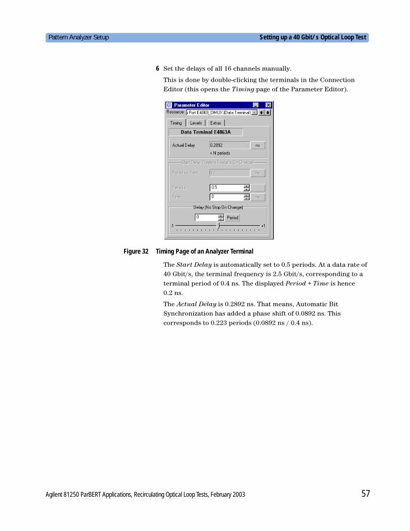
6 Set the delays of all 16 channels manually.
This is done by double-clicking the terminals in the Connection Editor (this opens the Timing page of the Parameter Editor).
Figure 32 Timing Page of an Analyzer Terminal
The Start Delay is automatically set to 0.5 periods. At a data rate of 40 Gbit/s, the terminal frequency is 2.5 Gbit/s, corresponding to a terminal period of 0.4 ns. The displayed Period + Time is hence 0.2 ns.
The Actual Delay is 0.2892 ns. That means, Automatic Bit Synchronization has added a phase shift of 0.0892 ns. This corresponds to 0.223 periods (0.0892 ns / 0.4 ns).
Agilent 81250 ParBERT Applications, Recirculating Optical Loop Tests, February 2003 57
Setting up a 40 Gbit/s Optical Loop Test Pattern Analyzer Setup
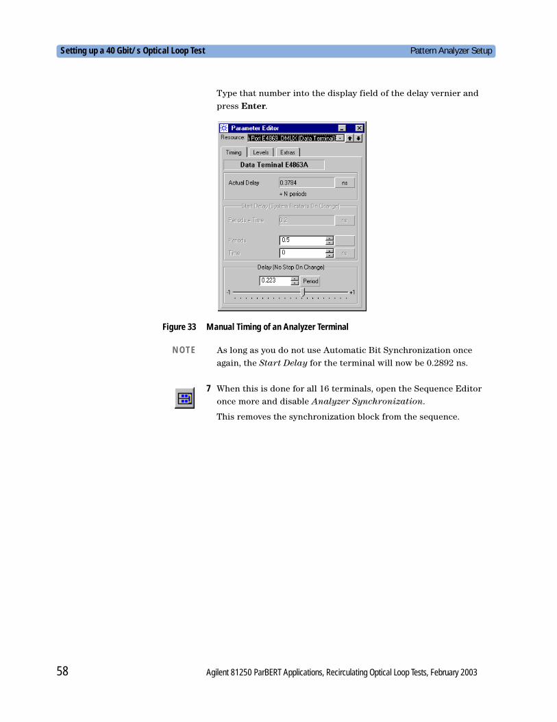
Type that number into the display field of the delay vernier and press Enter.
Figure 33 Manual Timing of an Analyzer Terminal
NO TE As long as you do not use Automatic Bit Synchronization once again, the Start Delay for the terminal will now be 0.2892 ns.
7 When this is done for all 16 terminals, open the Sequence Editor once more and disable Analyzer Synchronization.
This removes the synchronization block from the sequence.
58 Agilent 81250 ParBERT Applications, Recirculating Optical Loop Tests, February 2003
Pattern Analyzer Setup Setting up a 40 Gbit/s Optical Loop Test
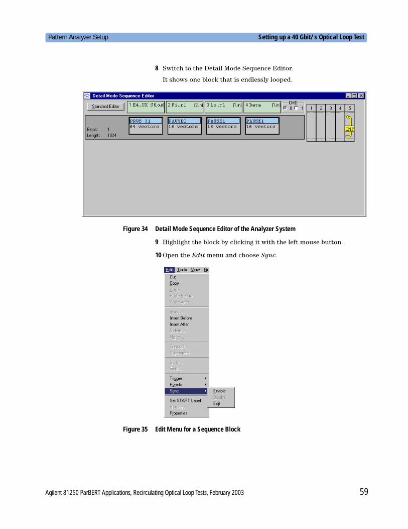
8 Switch to the Detail Mode Sequence Editor.
It shows one block that is endlessly looped.
Figure 34 Detail Mode Sequence Editor of the Analyzer System
9 Highlight the block by clicking it with the left mouse button.
10 Open the Edit menu and choose Sync.
Figure 35 Edit Menu for a Sequence Block
Agilent 81250 ParBERT Applications, Recirculating Optical Loop Tests, February 2003 59
Setting up a 40 Gbit/s Optical Loop Test Pattern Analyzer Setup
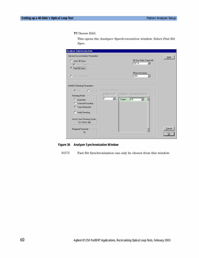
11 Choose Edit.
This opens the Analyzer Synchronization window. Select Fast Bit Sync.
Figure 36 Analyzer Synchronization Window
NO TE Fast Bit Synchronization can only be chosen from this window.
60 Agilent 81250 ParBERT Applications, Recirculating Optical Loop Tests, February 2003
Pattern Analyzer Setup Setting up a 40 Gbit/s Optical Loop Test
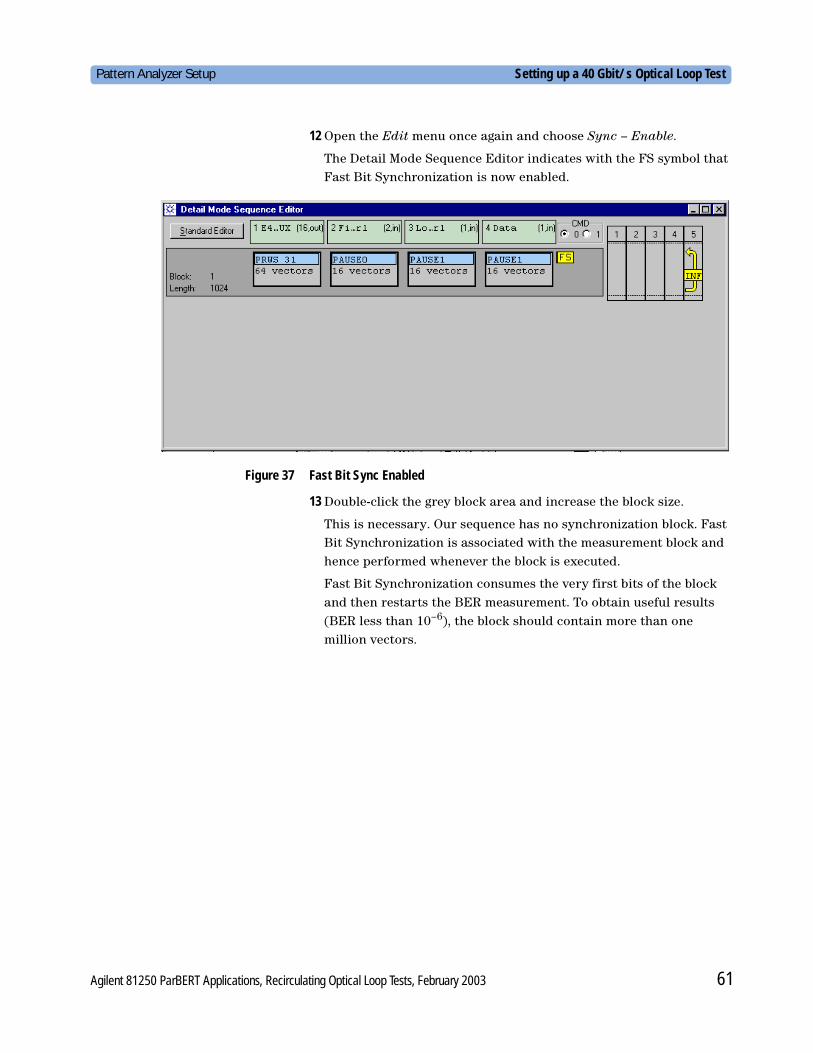
12 Open the Edit menu once again and choose Sync – Enable.
The Detail Mode Sequence Editor indicates with the FS symbol that Fast Bit Synchronization is now enabled.
Figure 37 Fast Bit Sync Enabled
13 Double-click the grey block area and increase the block size.
This is necessary. Our sequence has no synchronization block. Fast Bit Synchronization is associated with the measurement block and hence performed whenever the block is executed.
Fast Bit Synchronization consumes the very first bits of the block and then restarts the BER measurement. To obtain useful results (BER less than 10–6), the block should contain more than one million vectors.
Agilent 81250 ParBERT Applications, Recirculating Optical Loop Tests, February 2003 61
Setting up a 40 Gbit/s Optical Loop Test Pattern Analyzer Setup
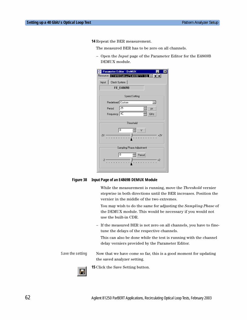
14 Repeat the BER measurement.
The measured BER has to be zero on all channels.
– Open the Input page of the Parameter Editor for the E4869B DEMUX module.
Figure 38 Input Page of an E4869B DEMUX Module
While the measurement is running, move the Threshold vernier stepwise in both directions until the BER increases. Position the vernier in the middle of the two extremes.
You may wish to do the same for adjusting the Sampling Phase of the DEMUX module. This would be necessary if you would not use the built-in CDR.
– If the measured BER is not zero on all channels, you have to fine-tune the delays of the respective channels.
This can also be done while the test is running with the channel delay verniers provided by the Parameter Editor.
Save the setting Now that we have come so far, this is a good moment for updating the saved analyzer setting.
15 Click the Save Setting button.
62 Agilent 81250 ParBERT Applications, Recirculating Optical Loop Tests, February 2003
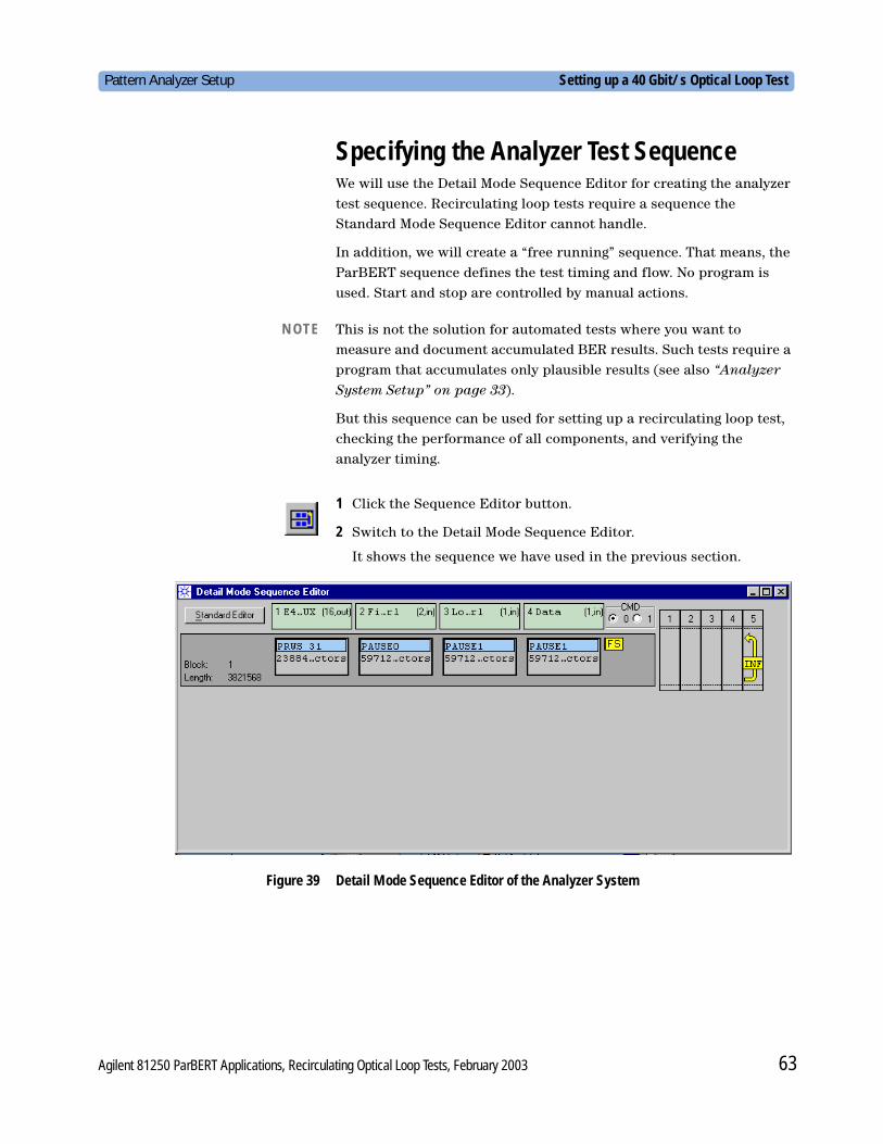
Pattern Analyzer Setup Setting up a 40 Gbit/s Optical Loop Test
Specifying the Analyzer Test SequenceWe will use the Detail Mode Sequence Editor for creating the analyzer test sequence. Recirculating loop tests require a sequence the Standard Mode Sequence Editor cannot handle.
In addition, we will create a “free running” sequence. That means, the ParBERT sequence defines the test timing and flow. No program is used. Start and stop are controlled by manual actions.
NOTE This is not the solution for automated tests where you want to measure and document accumulated BER results. Such tests require a program that accumulates only plausible results (see also “Analyzer System Setup” on page 33).
But this sequence can be used for setting up a recirculating loop test, checking the performance of all components, and verifying the analyzer timing.
1 Click the Sequence Editor button.
2 Switch to the Detail Mode Sequence Editor.
It shows the sequence we have used in the previous section.
Figure 39 Detail Mode Sequence Editor of the Analyzer System
Agilent 81250 ParBERT Applications, Recirculating Optical Loop Tests, February 2003 63
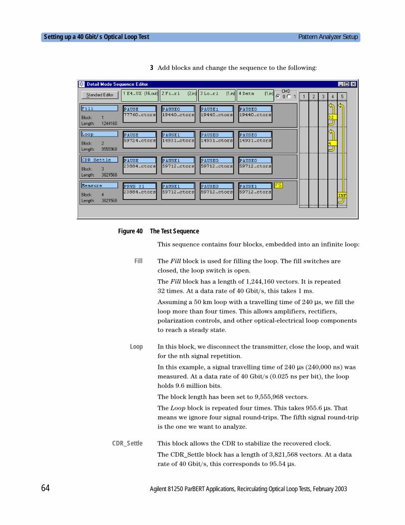
Setting up a 40 Gbit/s Optical Loop Test Pattern Analyzer Setup
3 Add blocks and change the sequence to the following:
Figure 40 The Test Sequence
This sequence contains four blocks, embedded into an infinite loop:
Fill The Fill block is used for filling the loop. The fill switches are closed, the loop switch is open.
The Fill block has a length of 1,244,160 vectors. It is repeated 32 times. At a data rate of 40 Gbit/s, this takes 1 ms.
Assuming a 50 km loop with a travelling time of 240 µs, we fill the loop more than four times. This allows amplifiers, rectifiers, polarization controls, and other optical-electrical loop components to reach a steady state.
Loop In this block, we disconnect the transmitter, close the loop, and wait for the nth signal repetition.
In this example, a signal travelling time of 240 µs (240,000 ns) was measured. At a data rate of 40 Gbit/s (0.025 ns per bit), the loop holds 9.6 million bits.
The block length has been set to 9,555,968 vectors.
The Loop block is repeated four times. This takes 955.6 µs. That means we ignore four signal round-trips. The fifth signal round-trip is the one we want to analyze.
CDR_Settle This block allows the CDR to stabilize the recovered clock.
The CDR_Settle block has a length of 3,821,568 vectors. At a data rate of 40 Gbit/s, this corresponds to 95.54 µs.
64 Agilent 81250 ParBERT Applications, Recirculating Optical Loop Tests, February 2003
Running the Test Setting up a 40 Gbit/s Optical Loop Test
Measure This block will be used for both Fast Bit Synchronization and the BER measurement. The expected data is the generated PRWS. Ensure that Fast Bit Synchronization is enabled.
The Measure block is executed once. Its length determines the duration of the analysis.
In the figure above, it has a length of 3,821,568 vectors. At a data rate of 40 Gbit/s, this corresponds to an analysis time of 95.54 µs. The remaining data of the signal round-trip (48.9 µs) is discarded.
TIP You can see how the timing requirements are translated into block lengths and vice versa.
When the first test was successful, you can optimize the timing—for example, by tuning the Loop time, decreasing the CDR_Settle time, and increasing the Measure time.
Running the Test
This is a standard ParBERT procedure:
1 Open the Bit Error Rate display.
2 Click the Run button.
3 Observe the BER counters.
Before running the test, you may wish to adjust the Bit Error Rate display to your needs.
Customizing the Bit Error Rate display In this example, we will not inspect the accumulated results. One single bit error during the Fast Bit Synchronization would make them obsolete.
We want to observe the instantaneous, updated results of every measurement. We do not want to be distracted by useless information.
You can easily adapt the Bit Error Rate display to your requirements:
1 Click the title of a column.
A red vertical bar appears.
2 Drag the column to the desired position.
Agilent 81250 ParBERT Applications, Recirculating Optical Loop Tests, February 2003 65
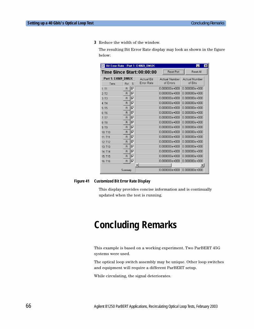
Setting up a 40 Gbit/s Optical Loop Test Concluding Remarks
3 Reduce the width of the window.
The resulting Bit Error Rate display may look as shown in the figure below:
Figure 41 Customized Bit Error Rate Display
This display provides concise information and is continually updated when the test is running.
Concluding Remarks
This example is based on a working experiment. Two ParBERT 45G systems were used.
The optical loop switch assembly may be unique. Other loop switches and equipment will require a different ParBERT setup.
While circulating, the signal deteriorates.
66 Agilent 81250 ParBERT Applications, Recirculating Optical Loop Tests, February 2003
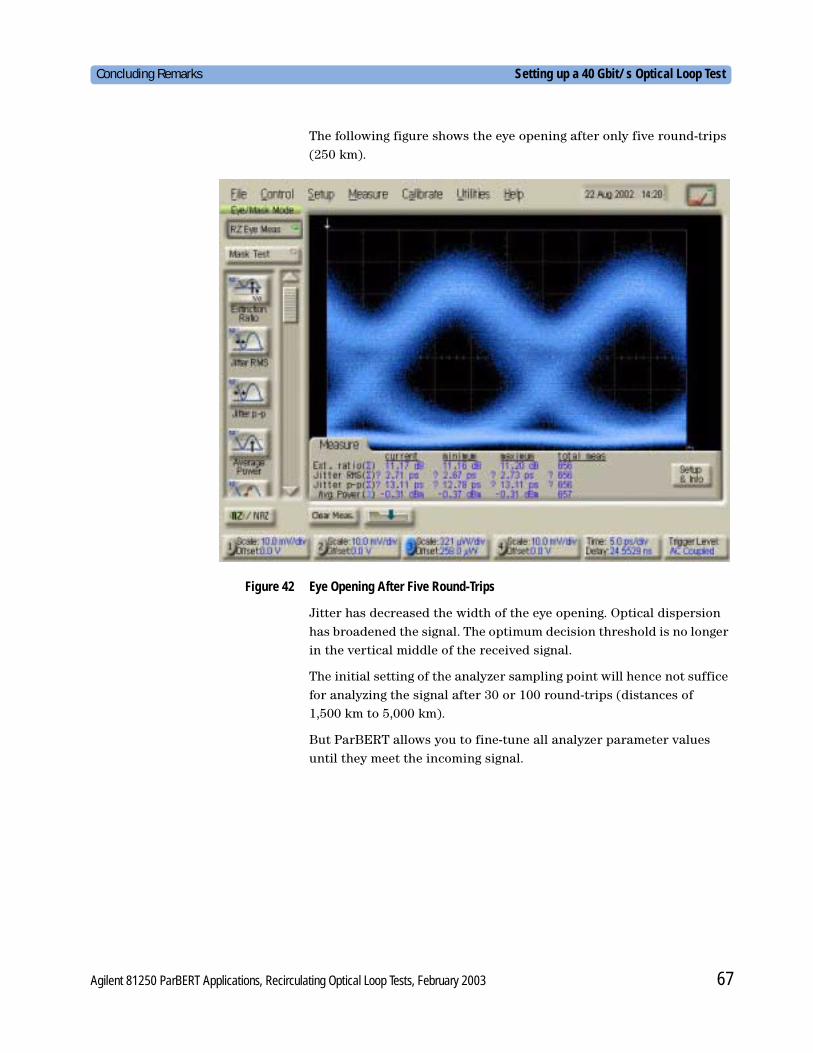
Concluding Remarks Setting up a 40 Gbit/s Optical Loop Test
The following figure shows the eye opening after only five round-trips (250 km).
Figure 42 Eye Opening After Five Round-Trips
Jitter has decreased the width of the eye opening. Optical dispersion has broadened the signal. The optimum decision threshold is no longer in the vertical middle of the received signal.
The initial setting of the analyzer sampling point will hence not suffice for analyzing the signal after 30 or 100 round-trips (distances of 1,500 km to 5,000 km).
But ParBERT allows you to fine-tune all analyzer parameter values until they meet the incoming signal.
Agilent 81250 ParBERT Applications, Recirculating Optical Loop Tests, February 2003 67

Setting up a 40 Gbit/s Optical Loop Test Concluding Remarks
68 Agilent 81250 ParBERT Applications, Recirculating Optical Loop Tests, February 2003
Index
Index
A
Acousto-optical modulator 10
Analyzer Sampling Delay Setup 54
analyzer setup 33
Analyzer synchronization 13
Analyzer System Clock Setup 52
Analyzer Test Sequence setup 63
AOM 10
Application Overview 5
B
BERT 12
Burst mode 8
Burst Mode Timing Calculation Example 16
C
cable delay compensation 51
CDR 7, 13
Clock data recovery 7
Continuous mode 11
Continuous Mode Timing Calculation Example 18
Customizing the Bit Error Rate display 65
D
delay compensation 51
E
EMI Loop Switch 10
EMI loop switch 5
Events 34
F
Fast Bit Synchronization 14
Frequency and Phase Synchronization 13
FS symbol 35, 39, 61
L
Loopoptical 6
Loop switch 7, 10
M
Measurementphases 6principle 6
Measurement modeburst mode 8continuous mode 11
O
Opticalloop switch 7
Optical loop 6
Optical receiver 7
Optical transmitter 7
P
Phase velocity of light 9
Phases of measurement 6
PLL 13
PRBS 7
Precision and Test Duration 9
Principle of measurement 6
Principle of Timing Calculations 15
R
Receiver 7
S
Sampling Point Adjustment 13
Select Fast Bit SynchronizationEnabling 60
Setup Procedures 30Analyzer setup 33transmitter setup 30
Speed of light 9
T
Test Environment 20
Test ExampleHardware Setup 43Pattern Analyzer Setup 50Pattern Generator Setup 45
Test exampleParBERT setup 44
Timing calculations 15
Transmitter 7
transmitter setup 30
Trigger pod 34
Agilent 81250 ParBERT Applications, Recirculating Optical Loop Tests, February 2003 69
S1
Copyright Agilent Technologies 2003Printed in Germany February 2003
5988-8675EN


![RECIRCULATING LOOP CHILLERS - | Filtrine Manufacturing [PCP-1000S].pdf · RECIRCULATING LOOP CHILLERS MODELS ... • POC - Open Loop Chillers - pump liquid from an open tank or sump,](https://img.pdfslide.net/doc/110x75/5ae70df17f8b9a08778dd23b/recirculating-loop-chillers-filtrine-manufacturing-pcp-1000spdfrecirculating.jpg)