Embed Size (px)
Citation preview
Recollections of Early Chip Development at Intel 1
Recollections of Early Chip Development at Intel
Andrew M. Volk, Desktop Platforms Group, Intel Corp. Peter A. Stoll, Technology & Manufacturing Group, Intel Corp.
Paul Metrovich, Desktop Platforms Group, Intel Corp.
Index words: history, products, naming, definition, validation, debug
ABSTRACT In the early days of Intel, between the late 1960s and the late 1970s, there was a regular product naming scheme by which a process, product type, or product family could be easily known. Few remain at Intel who remember this scheme, and its source is all but forgotten. The naming scheme and many stories of early products were uncovered through interviews and reminiscences by the authors, who among them have over 80 years of experience at Intel. This is their story.
INTRODUCTION The genesis for this paper came from a seemingly simple inquiry to the Intel® Technology Journal. A reader wanted to know why “80” was used in the name of all microprocessors until the Intel Pentium processor. This started a search for the origins of the naming system used in the early days at Intel. It also got a few of us thinking about the early products on which we worked. In this paper, we discuss some interesting and little known facts about products introduced in Intel’s first ten years, the way they were defined, developed, verified, and debugged, and how they contrast with the methods that we use today.
EARLY INTEL® PRODUCT NAMING SCHEME It surprised us that something as simple and mundane as the source of the early Intel® product naming scheme could be so hard to track down, but it was. In the end, we had to ask Dr. Andrew Grove, Chairman of the Board and one of the founders of Intel, for the answer. Dr. Grove said that he and Les Vadasz, then head of Engineering, worked it out one day in 1968. “I distinctly remember us concocting this scheme (minus 4XXX) sitting in his office in Mountain View, California. It worked well until
marketing decided to jazz it up with 4’s and 8’s” [1]. Dr. Gordon Moore also was “one of the cooks” that developed the naming system [2]. So that’s how it started.
Intel started with two processes: a PMOS polysilicon gate and a Schottky barrier diode bipolar process. One goal of the early products was to replace magnetic core memory in computers with silicon memories. To that end, the first products were a 64-bit bipolar memory and a 256-bit PMOS memory. The PMOS products were given numbers starting with 1xxx, and the bipolar products were given numbers starting with 3xxx. The second digit was a “1” for Random Access Memory (RAM), and the last two digits were the product sequence number. The sequence numbers of early products tended to start with “01” and went up from there. So, the first PMOS RAM was an 1101, and the first bipolar RAM was a 3101.
The 2xxx sequence started with an ambitious project to put a decoder and four 1101 RAM chips on a silicon substrate to make a 1-kilobit RAM module. The decoder was a bipolar product, the 2201, and the 2000 series was to be for hybrid products. However, the multichip module was not a success because of manufacturing difficulties and was therefore dropped. In 1971, the 2xxx sequence was given over to NMOS products.
Another form of memory was the Read-Only Memory (ROM). The first of these was a metal mask programmable 1-kilobit (256 x 4) bipolar part. The second digit “3” was assigned to ROMs. Therefore, the first bipolar ROM became the 3301, which incidentally proved to be a great source of revenue for Intel.
Intel also made shift register memory products. These were used mostly in video displays including Intel’s own Microcomputer Development Systems (MDS). Intel made several early shift registers up to 1-kilobit in size. These were all dynamic memories that required that the
Intel Technology Journal Q1, 2001
Recollections of Early Chip Development at Intel 2
clocks be kept running. The second digits “4” and “5” were assigned to shift registers, i.e., 1402 and 1405/1505.
Programmable ROMs (PROMs) were, and continue to be, key products for Intel. Again, both bipolar and PMOS versions were developed in the early days. The bipolar parts used polysilicon fuses that were blown by pulses of high current. The PMOS memories stored charge on a floating gate. PROMs that could only be programmed once were given “6” as the second digit. The PMOS PROMs could also be erased using ultraviolet light. These erasable PROMs (EPROMs) were assigned “7” as the second digit.
The very early products were sequentially numbered. However, memory chips were soon numbered in a manner to suggest their bit size, as can be seen in the sequence of EPROM names: 2704, 2708, 2716, on up to 27512. Wanting to keep the name to no more than 5 numbers long, the 1-megabit EPROM became the 27010.
The story of the 4004 microprocessor is well known [3, 4]. The name was a marketing decision to make the 4-bit architecture clear. It wasn’t an easy sell in 1971, and even in 1975 the Intel® Data Catalog introduced the Microcomputer section with two pages entitled “Why use a Microcomputer?” [5] All products associated with the 4004 were given numbers in the 4xxx sequence. Even existing products such as RAMs, ROMs, and PROMs were given 4004 family numbers, besides their normal family numbers.
In 1972, Intel acquired Microma Universal, Inc. and started in the watch business. The circuits required for these watches needed to be very low power. Consequently, a CMOS process was developed. CMOS products were assigned the “5xxx” designation. Chips that didn’t have oscillators were “52xx”, and chips that worked with a crystal were “58xx.” Later, this CMOS process was also used for the 5101 RAM.
Also in 1972, Intel built a PMOS 8-bit microprocessor for Computer Terminals Corporation (later Datapoint). Using the same naming scheme as the 4004, this chip was the 8008. Similarly, all support chips, RAM, ROM and EPROM, for the 8008 were included in the “8xxx” family. However, the 8008 was not particularly easy to use, and a more powerful NMOS microprocessor was introduced in 1974, the 8080. This name was a simple manipulation of the same numbers. The 8080 required +12, +5, and –5 volt supplies to run. Intel also produced the three support chips that drove the 12-volt clocks and decoded the bus control signals. In 1976, a 5-volt only version that integrated the support chips was introduced. Because it required only five volts, it was dubbed the 8085. This numbering scheme continued with the 8086, introduced in 1978. Les Vadasz recalled that the name sounded good to the marketing folks as it alluded to the 16-bit architecture [6]. The expense of having a 16-bit system was reduced by the introduction of the 8088 a year later. This was a quick spin of the 8086 to reduce the external data bus to 8 bits (hence the name). IBM’s choice of the 8086/88 architecture for its PC made the 8086 name extremely valuable. Subsequent processors
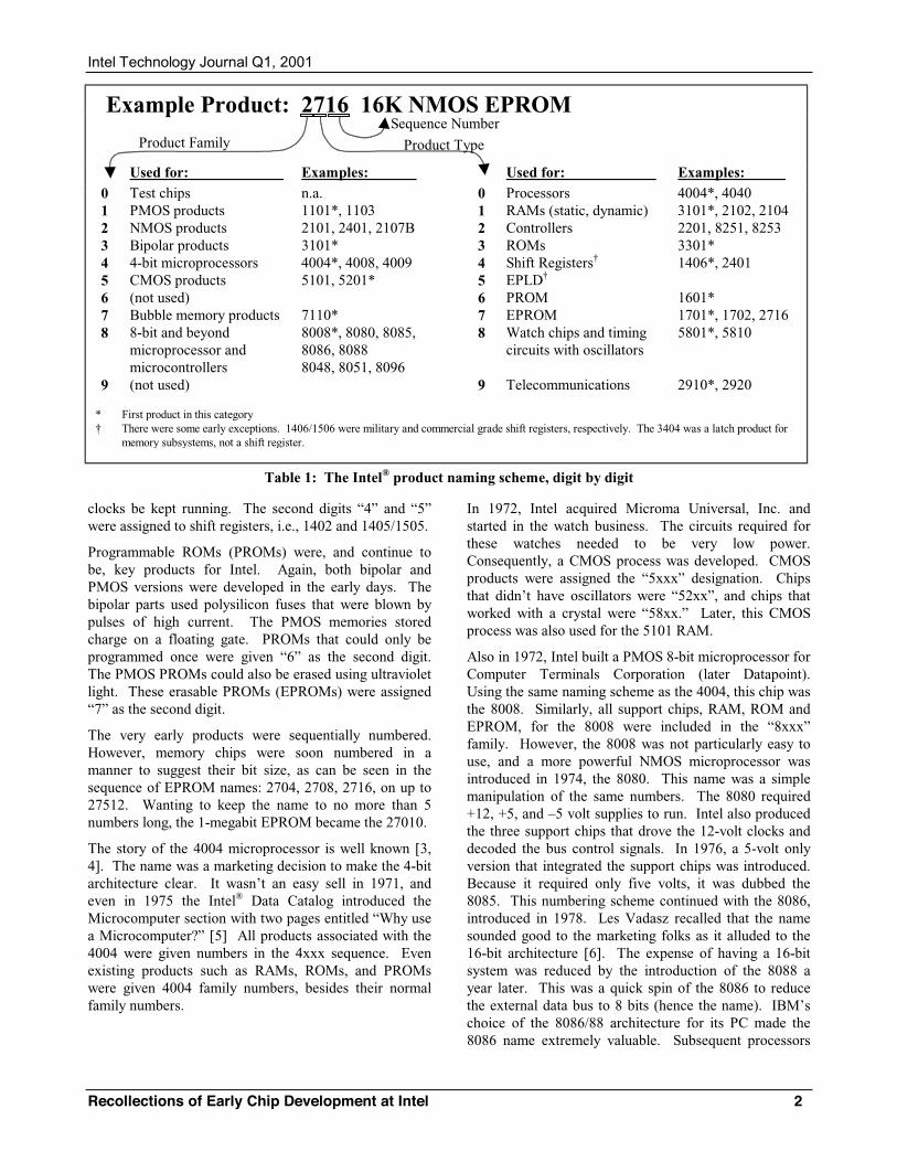
Table 1: The Intel® product naming scheme, digit by digit
Used for: Examples: Used for: Examples: 0 Test chips n.a. 0 Processors 4004*, 4040 1 PMOS products 1101*, 1103 1 RAMs (static, dynamic) 3101*, 2102, 2104 2 NMOS products 2101, 2401, 2107B 2 Controllers 2201, 8251, 8253 3 Bipolar products 3101* 3 ROMs 3301* 4 4-bit microprocessors 4004*, 4008, 4009 4 Shift Registers† 1406*, 2401 5 CMOS products 5101, 5201* 5 EPLD† 6 (not used) 6 PROM 1601* 7 Bubble memory products 7110* 7 EPROM 1701*, 1702, 2716 8 8-bit and beyond
microprocessor and microcontrollers
8008*, 8080, 8085, 8086, 8088 8048, 8051, 8096
8 Watch chips and timing circuits with oscillators
5801*, 5810
9 (not used) 9 Telecommunications 2910*, 2920 * First product in this category † There were some early exceptions. 1406/1506 were military and commercial grade shift registers, respectively. The 3404 was a latch product for
memory subsystems, not a shift register.
Product Family Product Type Sequence Number
Example Product: 2716 16K NMOS EPROM
Intel Technology Journal Q1, 2001
Recollections of Early Chip Development at Intel 3
went to 5-digit names to keep the 8086 name: 80286, 80386, and 80486. However, Intel could not get the “x86” sequence trademarked, and so the Intel Pentium processor name was born.
Because of the success of the microprocessor, the 8xxx product family has the most diverse set of products, including microcontrollers (8048, 8051, 8096) and peripheral controllers for all forms of microprocessor system functions and I/O. The first 8080 peripheral controllers were a serial I/O controller, a parallel I/O port, and a timer counter. The initial names for these chips also started out as 8201, 8202 etc., as did the early RAM chips. However, naming conflicts occurred when 3xxx family support products were renamed for use in the 8xxx family. These products were renamed 8251, 8255, and 8253 even before the designs were completed.
The last products to be assigned names were the telecommunications and analog products that used the second digit “9”. The 2910 was the first single chip CODEC and was introduced in 1977. Intel also entered the bubble memory business in 1977. The “7xxx” product family was reserved for bubble memory products, and the 7110 1-megabit bubble memory chip was introduced in 1979.
And there you have it; that’s how the early products were named and how the current naming scheme came about. But this is not the end of our story. Behind these product numbers are some little known histories, including some stories of products that were never in Intel’s Data Catalogs. Sit back as the authors reminisce and interview other early Intel employees.
THE AUTHORS’ PATHS TO INTEL Paul Metrovich joined Intel on a bet. He was working for Union Carbide Semiconductor when that company decided to relocate to San Diego. They had subleased the building with most of the fab equipment intact to Intel. The rumor mill had it that Intel had agreed with Union Carbide not to take applications from their employees until they were ready to move their operation to San Diego. Paul bet his fellow employees $5 that the agreement did not exist. He proceeded to apply for a job, and after several interviews with Intel, he secured a position. Paul started work on April 16, 1969. He never collected on his bet.
Peter Stoll studied Electrical Engineering at MIT between 1967 and 1974, where he took several courses on circuit design, integrated circuits, and semiconductor processing. He also did a seven-month internship at Bell Telephone Laboratories working in integrated circuit design. He was not very pleased with the experience, and swore off
semiconductor work when he returned to MIT for graduate school.
It did not help that the Electrical Engineering faculty at MIT in the early 1970s regarded design work with deep disdain. After a couple of years in biomedical instrumentation development, Peter realized that he didn’t have the heart to pursue a multiyear Ph.D. thesis. He decided to leave school, and Intel was the only company on the interview schedule between Thanksgiving and Christmas that had compatible needs. The Intel interviewers were much more interested in Peter's design background than MIT had been and they invited him to visit. The trip resulted in two job offers. He joined in 1974 as a one-man design team designing a watch chip for Microma: the 5810.
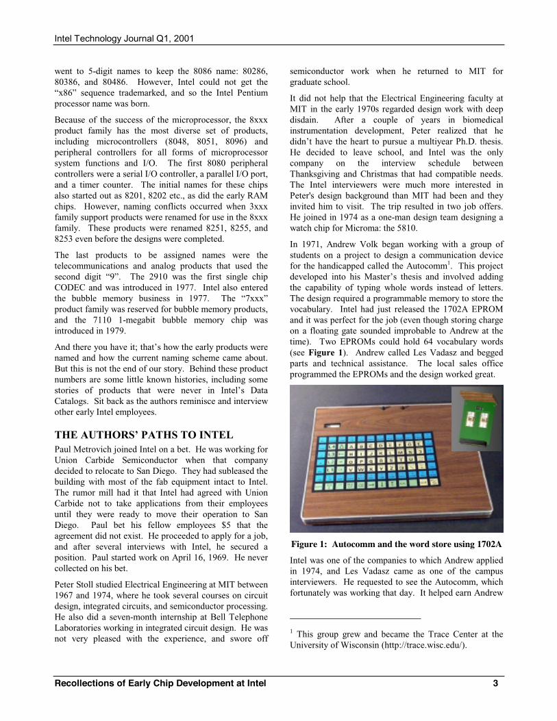
In 1971, Andrew Volk began working with a group of students on a project to design a communication device for the handicapped called the Autocomm1. This project developed into his Master’s thesis and involved adding the capability of typing whole words instead of letters. The design required a programmable memory to store the vocabulary. Intel had just released the 1702A EPROM and it was perfect for the job (even though storing charge on a floating gate sounded improbable to Andrew at the time). Two EPROMs could hold 64 vocabulary words (see Figure 1). Andrew called Les Vadasz and begged parts and technical assistance. The local sales office programmed the EPROMs and the design worked great.
Figure 1: Autocomm and the word store using 1702A
Intel was one of the companies to which Andrew applied in 1974, and Les Vadasz came as one of the campus interviewers. He requested to see the Autocomm, which fortunately was working that day. It helped earn Andrew
1 This group grew and became the Trace Center at the University of Wisconsin (http://trace.wisc.edu/).
Intel Technology Journal Q1, 2001
Recollections of Early Chip Development at Intel 4
a trip to California and a job offer. He started on July 1, 1974, working on the 8080A.
EARLY CUSTOM PRODUCTS It takes time to build a market and revenue, so Intel accepted several interesting custom products in the early days. The most famous of these was the offer by Busicomm to make a 12-chip calculator chipset. Of course this led to the 4004 and microprocessor history2. Even the 8008 was a custom job that turned into a standard product.
Custom products also got Intel started in the dynamic RAM business. Intel worked with Honeywell on a product called the 1102 (PMOS RAM number 2). Bill Regitz was with Honeywell at the time and was hired by Intel to work on an improved part, the 1103. Everybody, including Paul Metrovich, got in on the act of trying to make this beast work reliably. Intel had a ready-made market for those parts that didn’t quite meet the refresh rate specification: its Memory Systems Division. They just adjusted the refresh rate to whatever was necessary. In the end, the 1103 was a tremendous financial success.
There are plenty of lesser-known products. Tom Innes, Intel employee #38, recalls doing bipolar register and arithmetic unit chips for Burroughs Corp in 1970 (the 3405 and 3406, respectively) [7]. These were Complementary Transistor Logic (CTL) that used PNP inputs and emitter-follower outputs for high-speed and high-drive strength. Burroughs bought these chips for ten years. Ted Jenkins, Intel employee #22, started development on zinc-sulfide LEDs that emit blue light [8]. Gerry Parker, Intel employee #99, finished the work, and Intel sold it to Monsanto. We also developed a custom 7-segment decoder driver for a digital voltmeter they made. We only sold them 10,000 devices, a very small number in our business.
In 1972, Intel’s EPROM technology attracted the interest of Mars Money Systems (MMS) who wanted a chip for an electronic coin changer. MMS was a wholly owned subsidiary of Mars, Inc., the candy and food products company. Mars had gotten into the vending business quite early as a means to distribute their product. Accurate coin handling was critical to getting good revenue return as well as customer satisfaction. However, a good coin changer was a real Rube Goldberg3 contraption of delicately balanced levers and magnets.
2 See this history and others at the Intel Museum. Visit it on-line at http://www.intel.com/intel/intelis/museum/. 3 For those too young to know who Rube Goldberg is, see the web page at http://www.rube-goldberg.com/.
Fred Heiman, President of MMS at the time, invented an electronic means of differentiating coins using tuned coils. Using this scheme, Intel developed the 1205 and 1206 chips for MMS. We know the part number only because Paul Metrovich kept one as a souvenir in his toolbox. Paul worked on a prototype of discrete parts that proved the concept was feasible. Mr. Heiman recalls that it took less than one year to get it working and required about 3,000 transistors. He said that it worked wonderfully and had a product life of about five to six years. A coin reject solenoid was the only moving part in the coin mechanism [9].
Because the 1205/06 chip had an erasable PROM, it was self-calibrating. A replacement coin detector coil did not necessarily react the same as the previous one. The 1205/06 could be erased with ultraviolet light and a set of calibration coins fed through the coin changer to set the limits of detection. The results were programmed into the device while still in the vending machine. When new slugs were detected, their characteristics could be studied and new calibration coins developed to exclude them. MMS is now Mars Electronics, Inc. and still a large player in vending and coin, and in bill changing.
(Forest Mars, Sr., retiring head of Mars, Inc., visited Mr. Heiman about one year after the electronic coin mechanism went into production to understand it and its capabilities. He asked Mr. Heiman to arrange a meeting with the head of Intel and a meeting was set with Dr. Noyce a week later. He sat and listened to Bob talk about how Intel was growing and innovating on this “crest of technology.” That was enough for Mr. Mars to decide that he had no interest in buying Intel. He was used to developing long-term products with steadier sales than these new silicon devices that Intel was creating. Mr. Heiman noted, “Perhaps if the pace of silicon technology was a little slower, Intel might have become a division of Mars, Inc” [10]. No one at Intel was aware of this possibility, and as Les Vadasz noted “…we were not for sale, anyway” [11].)
One of Paul’s favorite custom parts was the 8244. It was a TV game chip that, when coupled with an 8048 microcontroller and a ROM, became the Magnavox “Odyssey 2.” It had a great nine holes of golf! Intel made good money on it. There was also an 8245 chip for European PAL television that differed from the 8244 only in the number of scan lines per frame and the timing of the TV sync outputs.
PRODUCT DEVELOPMENT IN THE DARK AGES If we compare the tools we had available to us 25-30 years ago to the tools we have today, we would definitely
Intel Technology Journal Q1, 2001
Recollections of Early Chip Development at Intel 5
call that period the dark ages of silicon development. The steps for developing a chip back then and now are much the same in a broad sense: definition, logic and circuit design, verification, layout and mask making, silicon wafer fabrication (processing), and debug and test. But that is where the similarity ends. In the early days, design, verification, and testing were done manually for the most part. Fortunately, the chip designs back then contained fewer than 30,000 transistors instead of today’s 42 million.
Today, chip definitions require specifications hundreds of pages long, logic design is largely a matter of writing software code, computers run millions of verification tests on logic and timing in a few days, and testing is done on multi-million dollar testers. This section describes some of our experiences with early chip development.
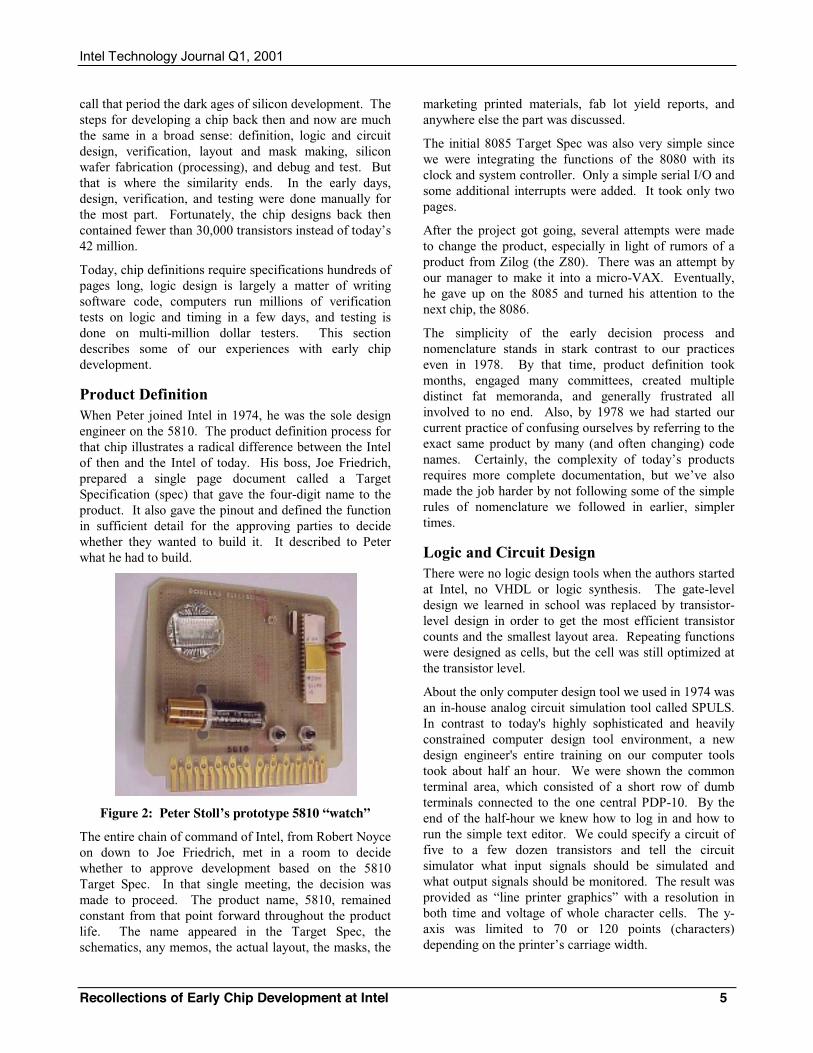
Product Definition When Peter joined Intel in 1974, he was the sole design engineer on the 5810. The product definition process for that chip illustrates a radical difference between the Intel of then and the Intel of today. His boss, Joe Friedrich, prepared a single page document called a Target Specification (spec) that gave the four-digit name to the product. It also gave the pinout and defined the function in sufficient detail for the approving parties to decide whether they wanted to build it. It described to Peter what he had to build.
Figure 2: Peter Stoll’s prototype 5810 “watch”
The entire chain of command of Intel, from Robert Noyce on down to Joe Friedrich, met in a room to decide whether to approve development based on the 5810 Target Spec. In that single meeting, the decision was made to proceed. The product name, 5810, remained constant from that point forward throughout the product life. The name appeared in the Target Spec, the schematics, any memos, the actual layout, the masks, the
marketing printed materials, fab lot yield reports, and anywhere else the part was discussed.
The initial 8085 Target Spec was also very simple since we were integrating the functions of the 8080 with its clock and system controller. Only a simple serial I/O and some additional interrupts were added. It took only two pages.
After the project got going, several attempts were made to change the product, especially in light of rumors of a product from Zilog (the Z80). There was an attempt by our manager to make it into a micro-VAX. Eventually, he gave up on the 8085 and turned his attention to the next chip, the 8086.
The simplicity of the early decision process and nomenclature stands in stark contrast to our practices even in 1978. By that time, product definition took months, engaged many committees, created multiple distinct fat memoranda, and generally frustrated all involved to no end. Also, by 1978 we had started our current practice of confusing ourselves by referring to the exact same product by many (and often changing) code names. Certainly, the complexity of today’s products requires more complete documentation, but we’ve also made the job harder by not following some of the simple rules of nomenclature we followed in earlier, simpler times.
Logic and Circuit Design There were no logic design tools when the authors started at Intel, no VHDL or logic synthesis. The gate-level design we learned in school was replaced by transistor-level design in order to get the most efficient transistor counts and the smallest layout area. Repeating functions were designed as cells, but the cell was still optimized at the transistor level.
About the only computer design tool we used in 1974 was an in-house analog circuit simulation tool called SPULS. In contrast to today's highly sophisticated and heavily constrained computer design tool environment, a new design engineer's entire training on our computer tools took about half an hour. We were shown the common terminal area, which consisted of a short row of dumb terminals connected to the one central PDP-10. By the end of the half-hour we knew how to log in and how to run the simple text editor. We could specify a circuit of five to a few dozen transistors and tell the circuit simulator what input signals should be simulated and what output signals should be monitored. The result was provided as “line printer graphics” with a resolution in both time and voltage of whole character cells. The y-axis was limited to 70 or 120 points (characters) depending on the printer’s carriage width.
Intel Technology Journal Q1, 2001
Recollections of Early Chip Development at Intel 6
In 1975-1977, when all of the original circuit design for the 8085 and 8086 microprocessors was carried out, the circuit size our central computer could handle was so small that we never simulated complete circuits or entire circuit paths. The circuit was decomposed into small pieces of about 5-20 transistors, simulated, and then added manually back together based on our understanding of the overall subsystem. The simulator was necessary for circuits such as RAM sense amplifiers, input buffers, and internal precharge-discharge buses.
The circuit size was limited by computing constraints such as memory. Another equally important size limit was the mean time to the computer crashing, which happened as often as every 15 minutes. If the computer went down, we lost the whole run. This also applied to file editing. There were no auto-backup files. We learned by brutal experience to save our work frequently.
There was, of course, no computer tool to extract parasitic capacitances from the actual layout, so accuracy in speed simulation was largely dependent on the design engineer's skill in guessing layout distances and routings.
Large portions of the logic circuitry of both the 8085 and 8086, as with other microprocessors and controller parts at that time, were composed of simple n-channel, depletion-load logic. On the 8085, Peter constructed a table estimating the delay for each size of depletion load transistor we used versus various circuit loads. This “paper computer” was used in place of circuit simulations for the overwhelming majority of the speed paths. The errors from these tables were quite small when the layout parasitic estimations were done reasonably well.
Breadboards and Prototypes Since simulation was limited, many other means were used to verify parts and new ideas. Paul remembers that the PMOS EPROMs were first prototyped by Dov Frohman, inventor of the EPROM, using a 4x4 array of discrete transistors in TO-5 packages on a special breadboard to enable programming and reading. A similar 16-bit array was put on to the first 1701, but since the full 256x8 array worked, the small array was never really tested [12].
Quite a few parts, ranging from the 1850-transistor 5810 watch chip, up to at least the 6144-transistor 8085 microprocessor, used no logic verification technique other than the engineer's brain. Andrew spent weeks in 1976 playing “computer” by running through all the 8085 instructions.
Several other development projects did construct a prototype breadboard, typically using commercial logic components such as 7400-series TTL to reproduce the
logic proposed for the chip. It was always difficult to get the breadboard done before the part was ready to tape out. Also, there were never commercial components available to reproduce all the functions we used on the chips. Breadboards were valuable to debug designs, and they provided a pre-silicon device to check the tester functionality. It was also valuable to check factors not easily seen on a simulation. We liked to use prototypes for human interface devices, like video displays or games.
Breadboarding was feasible until product device counts numbered in the tens of thousands of transistors. Eventually, the breadboard became too large and complicated to keep up with the speed of the real silicon product. The last custom breadboard Andrew and Paul constructed was a video terminal device, one of the first 5-digit (82730) part numbers in the early 1980s.
Ironically, a new form of breadboarding called emulation is being used now to verify chip designs with millions of transistors. The chips’ functions can be programmed by software into the emulator instead of having to solder or wirewrap discrete logic. Now we are able to essentially boot the PC without having to build any chips.
Logic Simulation Intel's first in-house logic simulator was LOLA/LOCIS, developed by a team headed by Mark Flomenhoft. It became ready for first use just in time to be used on the 8086 microprocessor project. Our use of this tool on the 8086 helped us find dozens of logic errors before the first stepping was taped out (although we did leave a few more to find in the actual silicon!). A parallel breadboard project consumed at least five times the staff, quite a bit more equipment, money, and lab space than the logic simulation effort, but the logic simulation effort found more problems sooner. (Jim McKevitt, lead designer on the 8086, found at least as many bugs using no tools other than his brain, the schematics, and a large supply of well-sharpened pencils.)
Layout and Mask Making Schematic and layout for the first ten years of Intel was done by hand. Engineers would produce draft schematics that a schematic designer would transfer onto D-sized vellum sheets. These would then be hand checked and signed off by the engineer. All edits to the schematic would be noted, checked, and signed off.
Layout planning was done between the engineers and the layout designer (mask designers). The layout of the 8085 was easier than most chips since it followed the base floorplan of the 8080. Peter guided most of the layout work, while Andrew did the layout of the control logic array. This was a ROM-like array based on a dual sum-
Intel Technology Journal Q1, 2001
Recollections of Early Chip Development at Intel 7
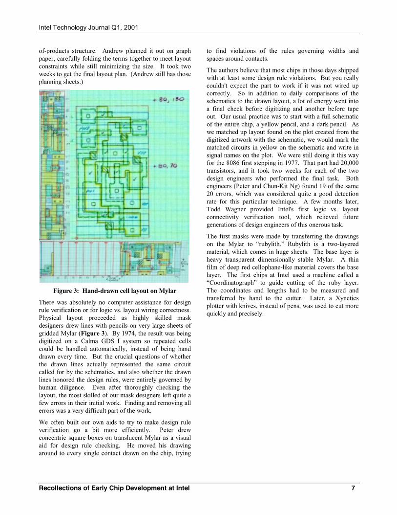
of-products structure. Andrew planned it out on graph paper, carefully folding the terms together to meet layout constraints while still minimizing the size. It took two weeks to get the final layout plan. (Andrew still has those planning sheets.)
Figure 3: Hand-drawn cell layout on Mylar
There was absolutely no computer assistance for design rule verification or for logic vs. layout wiring correctness. Physical layout proceeded as highly skilled mask designers drew lines with pencils on very large sheets of gridded Mylar (Figure 3). By 1974, the result was being digitized on a Calma GDS I system so repeated cells could be handled automatically, instead of being hand drawn every time. But the crucial questions of whether the drawn lines actually represented the same circuit called for by the schematics, and also whether the drawn lines honored the design rules, were entirely governed by human diligence. Even after thoroughly checking the layout, the most skilled of our mask designers left quite a few errors in their initial work. Finding and removing all errors was a very difficult part of the work.
We often built our own aids to try to make design rule verification go a bit more efficiently. Peter drew concentric square boxes on translucent Mylar as a visual aid for design rule checking. He moved his drawing around to every single contact drawn on the chip, trying
to find violations of the rules governing widths and spaces around contacts.
The authors believe that most chips in those days shipped with at least some design rule violations. But you really couldn't expect the part to work if it was not wired up correctly. So in addition to daily comparisons of the schematics to the drawn layout, a lot of energy went into a final check before digitizing and another before tape out. Our usual practice was to start with a full schematic of the entire chip, a yellow pencil, and a dark pencil. As we matched up layout found on the plot created from the digitized artwork with the schematic, we would mark the matched circuits in yellow on the schematic and write in signal names on the plot. We were still doing it this way for the 8086 first stepping in 1977. That part had 20,000 transistors, and it took two weeks for each of the two design engineers who performed the final task. Both engineers (Peter and Chun-Kit Ng) found 19 of the same 20 errors, which was considered quite a good detection rate for this particular technique. A few months later, Todd Wagner provided Intel's first logic vs. layout connectivity verification tool, which relieved future generations of design engineers of this onerous task.
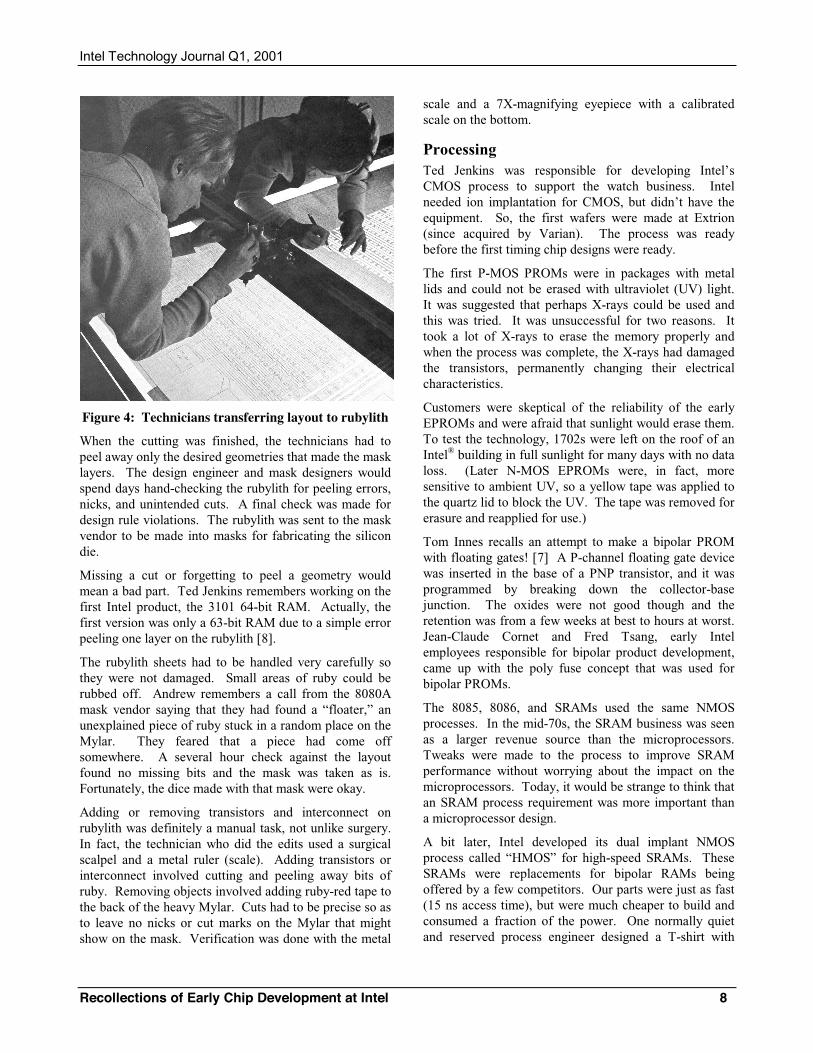
The first masks were made by transferring the drawings on the Mylar to “rubylith.” Rubylith is a two-layered material, which comes in huge sheets. The base layer is heavy transparent dimensionally stable Mylar. A thin film of deep red cellophane-like material covers the base layer. The first chips at Intel used a machine called a “Coordinatograph” to guide cutting of the ruby layer. The coordinates and lengths had to be measured and transferred by hand to the cutter. Later, a Xynetics plotter with knives, instead of pens, was used to cut more quickly and precisely.
Intel Technology Journal Q1, 2001
Recollections of Early Chip Development at Intel 8
Figure 4: Technicians transferring layout to rubylith
When the cutting was finished, the technicians had to peel away only the desired geometries that made the mask layers. The design engineer and mask designers would spend days hand-checking the rubylith for peeling errors, nicks, and unintended cuts. A final check was made for design rule violations. The rubylith was sent to the mask vendor to be made into masks for fabricating the silicon die.
Missing a cut or forgetting to peel a geometry would mean a bad part. Ted Jenkins remembers working on the first Intel product, the 3101 64-bit RAM. Actually, the first version was only a 63-bit RAM due to a simple error peeling one layer on the rubylith [8].
The rubylith sheets had to be handled very carefully so they were not damaged. Small areas of ruby could be rubbed off. Andrew remembers a call from the 8080A mask vendor saying that they had found a “floater,” an unexplained piece of ruby stuck in a random place on the Mylar. They feared that a piece had come off somewhere. A several hour check against the layout found no missing bits and the mask was taken as is. Fortunately, the dice made with that mask were okay.
Adding or removing transistors and interconnect on rubylith was definitely a manual task, not unlike surgery. In fact, the technician who did the edits used a surgical scalpel and a metal ruler (scale). Adding transistors or interconnect involved cutting and peeling away bits of ruby. Removing objects involved adding ruby-red tape to the back of the heavy Mylar. Cuts had to be precise so as to leave no nicks or cut marks on the Mylar that might show on the mask. Verification was done with the metal
scale and a 7X-magnifying eyepiece with a calibrated scale on the bottom.
Processing Ted Jenkins was responsible for developing Intel’s CMOS process to support the watch business. Intel needed ion implantation for CMOS, but didn’t have the equipment. So, the first wafers were made at Extrion (since acquired by Varian). The process was ready before the first timing chip designs were ready.
The first P-MOS PROMs were in packages with metal lids and could not be erased with ultraviolet (UV) light. It was suggested that perhaps X-rays could be used and this was tried. It was unsuccessful for two reasons. It took a lot of X-rays to erase the memory properly and when the process was complete, the X-rays had damaged the transistors, permanently changing their electrical characteristics.
Customers were skeptical of the reliability of the early EPROMs and were afraid that sunlight would erase them. To test the technology, 1702s were left on the roof of an Intel® building in full sunlight for many days with no data loss. (Later N-MOS EPROMs were, in fact, more sensitive to ambient UV, so a yellow tape was applied to the quartz lid to block the UV. The tape was removed for erasure and reapplied for use.)
Tom Innes recalls an attempt to make a bipolar PROM with floating gates! [7] A P-channel floating gate device was inserted in the base of a PNP transistor, and it was programmed by breaking down the collector-base junction. The oxides were not good though and the retention was from a few weeks at best to hours at worst. Jean-Claude Cornet and Fred Tsang, early Intel employees responsible for bipolar product development, came up with the poly fuse concept that was used for bipolar PROMs.
The 8085, 8086, and SRAMs used the same NMOS processes. In the mid-70s, the SRAM business was seen as a larger revenue source than the microprocessors. Tweaks were made to the process to improve SRAM performance without worrying about the impact on the microprocessors. Today, it would be strange to think that an SRAM process requirement was more important than a microprocessor design.
A bit later, Intel developed its dual implant NMOS process called “HMOS” for high-speed SRAMs. These SRAMs were replacements for bipolar RAMs being offered by a few competitors. Our parts were just as fast (15 ns access time), but were much cheaper to build and consumed a fraction of the power. One normally quiet and reserved process engineer designed a T-shirt with
Intel Technology Journal Q1, 2001
Recollections of Early Chip Development at Intel 9
appropriate graphics and the slogan: “Cure your blazing Bipolar itch with Preparation HMOS!”
HMOS was a very robust process. The first SRAMs made with HMOS were packaged in a white ceramic package. The parts were tested for reliability with a “life test” of 1000 hours in a burn-in oven at 125°C. For one batch of parts, the oven temperature control failed and got to over twice that temperature before being shut down. When the burn-in boards were removed, the sockets holding the parts had melted down the boards like wax. The parts themselves were the color of toasted brown marshmallows. Incredibly, the vast majority of parts survived quite well with little impact on their performance.
Test and Debug In the process of developing DRAMs, it became apparent that there was a need for specialized test equipment. Initially, engineers used simple switch boxes and fixtures with signal generators and viewed results on an oscilloscope. The wafer prober was operated by hand and bad dice were marked with a felt-tip pen. However, this arrangement soon proved too tedious, and commercial LSI test systems were purchased. These were rudimentary machines that came with a high price tag.
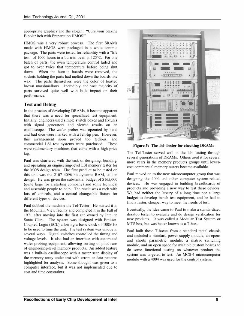
Paul was chartered with the task of designing, building, and operating an engineering-level LSI memory tester for the MOS design team. The first product to be tested on this unit was the 2107 4096 bit dynamic RAM, still in design. He was given the substantial budget of $165,000 (quite large for a starting company) and some technical and assembly people to help. The result was a rack with lots of controls, and a central changeable fixture for different types of devices.
Paul dubbed the machine the Tel-Tester. He started it in the Mountain View facility and completed it in the Fall of 1971 after moving into the first site owned by Intel in Santa Clara. The system was designed with Emitter-Coupled Logic (ECL) allowing a basic clock of 100MHz to be used to time the unit. The test system was unique in several ways. Digital switches controlled the timing and voltage levels. It also had an interface with automated wafer-probing equipment, allowing sorting of pilot runs of engineering-level memory products. An added feature was a built-in oscilloscope with a raster scan display of the memory array under test with errors or data patterns highlighted for analysis. Some thought was given to a computer interface, but it was not implemented due to cost and time constraints.
Figure 5: The Tel-Tester for checking DRAMs
The Tel-Tester served well in the lab, lasting through several generations of DRAMs. Others used it for several more years in the memory products groups until lower-cost commercial memory testers became available.
Paul moved on to the new microcomputer group that was designing the 4004 and other computer system-related devices. He was engaged in building breadboards of products and providing a new way to test these devices. We had neither the luxury of a long time nor a large budget to develop bench test equipment, and he had to find a faster, cheaper way to meet the needs of test.
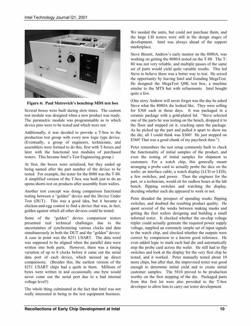
Eventually, the idea came to Paul to make a standardized desktop tester to evaluate and do design verification for new products. It was called a Modular Test System or MTS box, but was better known as a T-box.
Paul built these T-boxes from a standard metal chassis and included a standard power supply module, an opens and shorts parametric module, a matrix switching module, and an open space for multiple custom boards to do some functional testing on whatever product the system was targeted to test. An MCS-4 microcomputer module with a 4004 was used for the control system.
Intel Technology Journal Q1, 2001
Recollections of Early Chip Development at Intel 10
Figure 6: Paul Metrovich’s benchtop MDS test box
Several boxes were built during slow times. The custom test module was designed when a new product was ready. The parametric module was programmable as to which device pins were to be tested and which were not.
Additionally, it was decided to provide a T-box to the production test group with every new logic type device. (Eventually, a group of engineers, technicians, and assemblers were formed to do this, first with T-boxes and later with the functional test modules of purchased testers. This became Intel’s Test Engineering group.)
At first, the boxes were serialized, but they ended up being named after the part number of the device to be tested. For example, the tester for the 8080 was the T-80. A simplified version of the T-box was built just to do an opens/shorts test on products after assembly from wafers.
Another test concept was doing comparison functional testing between a “golden” device and the Device Under Test (DUT). This was a good idea, but it became a chicken-and-egg contest to find a device that was, in fact, golden against which all other devices could be tested.
Some of the “golden” device comparison testers presented real technical challenges due to the uncertainties of synchronizing various clocks and data simultaneously in both the DUT and the “golden” device. A case in point was the 8251 USART. The data word was supposed to be aligned when the parallel data were written into both parts. However, there was a timing variation of up to 8 clocks before it came out the serial data port of each device, which messed up direct comparisons. (Besides this, the earliest version of the 8251 USART chips had a quirk in them. Millions of bytes were written in and occasionally one byte would never come out the serial port due to a bad internal voltage level!)
The whole thing culminated in the fact that Intel was not really interested in being in the test equipment business.
We needed the units, but could not purchase them, and the large LSI testers were still in the design stages of development. Intel was always ahead of the support marketplace.
Steve Bissett, Andrew’s early mentor on the 8080A, was working on getting the 8080A tested on the T-80. The T-80 was not very reliable, and multiple passes of the same set of parts would yield quite variable results. This led Steve to believe there was a better way to test. He seized the opportunity by leaving Intel and founding MegaTest. He designed the MegaTest Q8K test box, a machine similar to the MTS but with refinements. Intel bought quite a few.
(One story Andrew will never forget was the day he asked Steve what the 8080A die looked like. They were selling for $360 each in those days. It was packaged in a ceramic package with a gold-plated lid. “Steve selected one of the parts he was testing on the bench, dropped it to the floor and stepped on it, cracking open the package. As he picked up the part and pulled it apart to show me the die, all I could think was $360! He just stepped on $360! That was a good chunk of my paycheck then.”)
Peter remembers the test setup commonly built to check the functionality of initial samples of the product, and even the testing of initial samples for shipment to customers. For a watch chip, this generally meant arranging a probe card to actually probe the dice on the wafer, an interface cable, a watch display (LCD or LED), a few switches, and power. Then the engineer for the part, or a technician, would sit for endless hours at the lab bench, flipping switches and watching the display, deciding whether each die appeared to work or not.
Peter dreaded the prospect of spending weeks flipping switches, and doubted the resulting product quality. He spent several of the weeks between making masks and getting the first wafers designing and building a small informal tester. It checked whether the on-chip voltage tripler could actually generate the required power supply voltage, supplied an extremely simple set of input signals to the watch chip, and checked whether the outputs were correct by comparison to a known good reference. He even added logic to mark each bad die and automatically step the probe card across the wafer. He still had to flip switches and look at the display for the very first chip he tested, and it worked. Peter manually tested about 10 more chips, but after that, the improvised tester was good enough to determine initial yield and to create initial customer samples. The 5810 proved to be production worthy on the first stepping of the die. Packaged parts from this first lot were also provided to the T-box developer to allow him to carry out tester development.
Intel Technology Journal Q1, 2001
Recollections of Early Chip Development at Intel 11
Peter got a bit of help in assembling his informal tester from one of the lab technicians, but he did nearly the entire chip checkout, evaluation, and sample generation himself. In those days, a product design engineer could expect to be heavily involved in nearly all phases of product development. For many of us, this relationship created a deep satisfaction and an intense sense of ownership.
Peter and Andrew also designed a test setup for the 8085 chip that was, in essence, a small computer system where the 8085 under test actually executed its own test program. This was a dangerous strategy since the part needed some functionality to even get the test started. Both the part and tester worked well enough to allow us to debug the chip from the start (after making an allowance for an inversion on the chip’s address bus tri-state control).
The dedication we all felt to the products can be demonstrated by a final story. The stepping of the 8085 that was expected to allow volume production of the part came out of the fab over a week earlier than expected, on October 21, 1976 to be precise. Andrew remembers that date well. It was the day before his wedding. But he still stayed until midnight checking out the new stepping. He left a short report on his boss’ chair saying that all the bugs found in the previous stepping were checked and working, and that he would do a more thorough evaluation—in a week!
CONCLUSION It is hard to end this story. Each time a name or event is mentioned, it triggers yet another episode buried somewhere in our memories. It has allowed us to briefly revisit a time when we were heavily involved mentally, physically, and emotionally in our work. It was a time when we felt we were entirely responsible for a project. Writing this has stirred feelings that have lain dormant for a long time, yet come flooding back upon hearing the stories, seeing the pictures, and talking with past colleagues.
There are many more articles and histories floating around in the minds of the good employees, present and past, who contributed to building and sustaining the corporation called Intel. Each individual has a story to tell, a joke to make you laugh, an incident to relate that evokes a touch of anger, and a personal anecdote that makes a career a life experience. To discover and recount all of these would take another lifetime and result in a large book rather than a journal article. For now, we just want to record some of our early experiences in a young corporation by highlighting how products were named and developed in the first years. We hope we
have done this in a way that brings across the fun we had, the effort we put in, and the results we achieved.
ACKNOWLEDGEMENTS It was a real challenge to find people who were around during the first years of Intel Corporation to check the information in this article. To those who contributed to this paper, thank you for sharing your life work and memories. Of particular assistance were Dr. Gordon Moore, Tom Innes, Ted Jenkins, and Les Vadasz who provided additional information and reviewed our article. We also got a final verification of the naming system from Dr. Andrew Grove (who was definitely here from the beginning). Dov Frohman provided insight on EPROM development and Mr. Fred Heiman gave us the inside story on the 1205 Mars Money Systems chip. Thanks also go to Tracey Mazur of the Intel® Museum for help with reference material. Peggy Thompson and Norman Strand get honors for still having examples of hand-drawn layout, the most having been long since scrapped. We also thank the Trace Center for providing photos of an early Autocomm.
REFERENCES [1] Grove, Andrew, “Question on history of product
numbering,” E-mail to Andrew Volk, Dec. 8, 2000.
[2] Moore, Gordon, telephone interview, Jan. 16, 2001.
[3] Noyce, R. and Hoff, T., “A History of Microprocessor Development at Intel,” IEEE Micro, Vol.1, No. 1, Feb. 1981, pp. 8-11, and 13-21.
[4] Freiberger, P. and Swaine, P., Fire in the Valley – The Making of the Personal Computer, Second Edition, McGraw-Hill, New York, NY, 2000, pp. 15-23.
[5] Intel Corporation, 1975 Data Catalog, Sect. 6, pp. 3-4.
[6] Vadasz, Les, telephone interview, Dec. 4, 2000.
[7] Innes, Tom, telephone interview, Dec. 8, 2000.
[8] Jenkins, Ted, telephone interview, Dec. 7, 2000.
[9] Heiman, Fred, telephone interview, Dec. 5, 2000.
[10] Heiman, Fred, “Interview notes on Mars chip,” E-mail to Andrew Volk, Dec. 7, 2000.
[11] Vadasz, Les, review comments on this paper for the Q1 Intel Technology Journal, quoted in an e-mail to Andrew Volk, Dec. 19, 2000.
[12] Frohman, Dov, “Search for old information,” e-mail to Paul Metrovich, Dec. 8, 2000.
Intel Technology Journal Q1, 2001
Recollections of Early Chip Development at Intel 12
AUTHORS’ BIOGRAPHIES Andrew Volk is a 26-year veteran of Intel. He started his design work on the 8080A. He was responsible for the logic design on the 8085 and has been lead designer and project manager for several I/O products for embedded control, bubble memories, and personal computers. Currently, he is a Principal Engineer responsible for developing special circuits especially as they apply to new technologies. He specializes in circuit design and physical interface definition for various buses. He was responsible for the electrical bus definition for the Universal Serial Bus (USB), Accelerated Graphics Port (AGP), and the link interface for the Intel Hub Architecture chipsets. Andrew is the holder of 19 patents with 23 pending, has written several technical articles and a chapter in a computer technology book, and has been a speaker at industry conferences. He joined Intel after receiving his Master's degree in Electrical and Computer Engineering from the University of Wisconsin. He enjoys reading, walking, fishing, and travel. His e-mail is [email protected].
Peter A. Stoll first joined Intel in 1974. He also joined Intel in 1978 and 1987! Peter's design engineering work included a watch chip, the circuit design of the 8085 microprocessor, and circuit design, logic simulation, and speedup stepping work on the 8086 microprocessor; and, a few days devising and implementing an emergency fix to the 80386 32-bit multiply problem. Peter also worked at Hewlett-Packard in high-speed GaAs logic circuit design. At Daisy Systems he was the primary developer of a hardware/software product allowing use of logic parts as their own models in logic simulations. Since 1988, Peter has worked in the Intel® Albuquerque wafer fabs in reliability, yield, and product engineering roles. He has worked most frequently on the large-scale use of available technical data from wafer and unit production to help resolve yield and reliability problems. Peter holds SB, SM, and EE degrees from the Massachusetts Institute of Technology, where he was admitted as a Presidential Scholar, and he was admitted to Eta Kappa Nu, Sigma Xi, and Tau Beta Pi honoraries. His e-mail is [email protected].
Paul Metrovich joined Intel on April 16, 1969, working in the Design Engineering department in the original Intel® site in Mountain View, California. He worked on the first dynamic shift registers and the 1103 DRAM. He also designed and built internal engineering test equipment (MTS) for DRAMs and early microprocessors, emulation breadboards of microprocessor support devices, and custom chips. Paul assisted with product design validation on such products as the 8251 and other system products based on the 8080/8085, along with
magnetic bubble memory support products and video games. He moved to Folsom, California in 1985 with the Peripherals group, assisting with debug and validation on floppy disk controllers and the PC chipset devices. Paul currently is the lab manager, designing and building specialty labs for the Chipset Engineering and Validation group. He received his electronics education in the U.S. Navy, and he has had prior employment at Varian Associates and Union Carbide Corp. His e-mail is [email protected].
Copyright © Intel Corporation 2001. This publication was downloaded from http://developer.intel.com/.
Legal notices at http://developer.intel.com/sites/developer/tradmarx.htm