Embed Size (px)
Citation preview
RECONFIGURABLE RADIO
FREQUENCY CIRCUITS
By
DEEPAK DOMALAPALLY,
Bachelor of Technology,Jawaharlal Nehru Technological University
Hyderabad, India2002
Submitted to the faculty of the Graduate College of the
Oklahoma State University in partial fulfillment of the requirements for
the degree of MASTER OF SCIENCE
May, 2005
i
RECONFIGURABLE RADIO
FREQUENCY CIRCUITS
Thesis Approved:

ii
ACKNOWLEDGEMENTS
I am greatly indebted to my thesis advisor Dr.Yumin Zhang for his intelligent
supervision, patience and constructive guidance. I would like to express my sincere
gratitude to Dr.Louis Johnson, Dr.Ramakumar for reviewing my thesis and serving as my
committee members.
I would also like to express my sincere gratitude to those who provided invaluable
suggestions and assistance for this study. I would like to thank all my WISS group
members for their support.
Finally I would like to thank my parents for supporting me all through my studies.
iii
TABLE OF CONTENTS
Chapter Page
1. INTRODUCTION………………………………………………………………….1
1.1 Introduction…………………………………………………………………...2 1.2 Organization of thesis…………………………………………………….......2
2. RECONFIGURABLE LOW NOISE AMPLIFIER………………………………..3
2.1 Low noise amplifier…………………………………………………………...3
2.1.1 Topology Selection…………………………………………………..4
2.2 Inductive source de-generated Low noise amplifier…………………………..6
2.2.1 Input impedance match……………………………………………....62.2.2 Load circuit…………………………………………………………..72.2.3 Voltage gain………………………………………………………….82.2.4 Noise Figure………………………………………………………….8 2.2.5 Noise Figure of Inductively source degenerated LNA……………..12 2.2.6 Linearity…………………………………………………………….13
2.3 Multi Band LNA……………………………………………………………..16
2.3.1 Load in multi mode LNAs………………………………………… 19
3. RECONFIGURABLE NEGATIVE RESISTANCE LC OSCILLATOR………...20
2.4 Choosing an Oscillator Architecture…………………………………………20
2.4.1 Oscillators as feedback systems…………………………………….202.4.2 LC oscillators……………………………………………………….22
iv
2.4.3 One port view of the oscillators…………………………………….232.4.4 NMOS only cross coupled LC oscillator…………………………...242.4.5 NMOS-PMOS cross coupled LC oscillator………………………...252.4.6 Analysis of NMOS-PMOS LC VCO………………………………28
2.5 Phase noise in oscillators…………………………………………………….32 2.6 Switching matrix network……………………………………………………34
4. RECONFIGURABLE CLASS E POWER AMPLIFIER………………………...38
2.7 Ideal Class E power amplifier………………………………………………..382.8 Principles for high efficiency…………………………………………….......39 2.9 Reconfigurable power amplifier……………………………………………..42
5. RECONFIGURABLE FILTER ………………………………………………......44
6. RESULTS AND CONCLUSIONS……………………………………………….46
2.10 Results of reconfigurable LNA………………………………………… 472.11 Results of reconfigurable oscillator……………………………………... 482.12 Results of reconfigurable filter………………………………………… 49 2.13 Results of reconfigurable power amplifier………………………………49
REFERENCES…………………………………………………………………….52

v
LIST OF FIGURES
Figure Page
2.1. Common gate amplifier……………………………………………………………..4
2.2. Common source amplifier with shunt input resistor………………………………...4
2.3. Shunt series amplifier……………………………………………………………….5
2.4. Narrow band LNA with inductive source degeneration………………………….. ..6
2.5. LC tank circuit………………………………………………………………………7
2.6. Thermal noise small signal circuit model of MOSFET……………………………..9
2.7. Induced gate noise model………………………………………………………......10
2.8. Small signal equivalent of LNA including the noise sources……………………...12
2.9. Illustration of LNA linearity parameters…………………………………………...14
2.10. A multi band low noise amplifier………………………………………………….15
2.11. Switched capacitor for LNA…………………………………………………….....16
2.12. A dual band low noise amplifier…………………………………………………...17
2.13. Load circuit in dual band LNA…………………………………………………….18
2.14. Schematic of reconfigurable LNA…………………………………………………20
2.15. S11 for frequency of 2.4 GHz……………………………………………………...22
2.16. S11 for frequency of 1.9GHz……………………………………………………....22
2.17. Noise figure for frequency of 2.4GHz……………………………………………..22
2.18. Noise figure for frequency of 1.9GHz……………………………………………..22

vi
2.19. S21 for frequency of 2.4 GHz……………………………………………………...23
2.20. S21 for frequency of 1.9 GHz……………………………………………………...23
2.21. IIP3 for frequency of 2.4 GHz…………………………………………………......23
2.22. IIP3 for frequency of 1.9 GHz…………………………………………………......23
3.1. Feedback system…………………………………………………………………...24
3.2 a) Ideal LC tuned circuit…………………………………………………………....26
3.2 b) Non ideal LC tuned circuit……………………………………………………....26
3.3. One port view of oscillator………………………………………………………...28
3.4. NMOS only cross coupled LC oscillator…………………………………………..30
3.5. NMOS-PMOS cross coupled LC oscillator………………………………………..33
3.6. Equivalent circuit of NMOS-PMOS cross coupled oscillator… ……………......35
3.7. LC oscillator showing the direction of currents…………………………………....37
3.8. Parallel bank of capacitors………………………………………………………....38
3.9. Switching matrix capacitor circuit………………………………………………....39
vii
3.10. Complete oscillator circuit………………………………………………………....41
3.11. Transient response of oscillator for the worst case
when all the switches are ON………………………………………………………42
3.12. Phase noise of the oscillator for the worst case condition…………………………43
4.1. Ideal Class E amplifier……………………………………………………………..46
4.2. Ideal switching characteristics of Class E power amplifier………………………..47
4.3. Proposed Reconfigurable power amplifier………………………………………...49
4.4. Tunable matching network at the output of power amplifier……………………...50
4.5. Complete proposed reconfigurable power amplifier………………………………51
4.6. Switching characteristics of Class E power amplifier when fo=2GHz………….....52
4.7. Switching characteristics of Class E power amplifier when fo=2GHz………….....53
4.8. PAE of proposed Class E power amplifier when fo=1GHz………………………..53
4.9. PAE of proposed Class E power amplifier when fo=0.5GHz……………………...53
4.10. Output response of the power amplifier when f0=2GHz ……………………….....54
4.11. Output response of the power amplifier when f0=2GHz ……………………….....54
5.1. Reconfigurable Filter………………………………………………………………55
5.2. Low pass frequency response of the filter…………………………………………56
5.3. Band pass frequency response of the filter…...........................................................56
5.4. High pass frequency response of the filter…………………………………………57
5.5. Band stop frequency response of the filter…………………………………….......58
viii
LIST OF TABLES
Table page
2.1 Table showing the performance metrics for the reconfigurable LNA………………………………………………………………..21
2.1 Digital control inputs for reconfiguring filter……………………………………...55
ix
NOMENCLATURE
SDR software defined radio
RF radio frequency
LNA low noise amplifier
NF noise figure
gm transconductance of mosfet
IIP3 third order interception point
1
CHAPTER-1
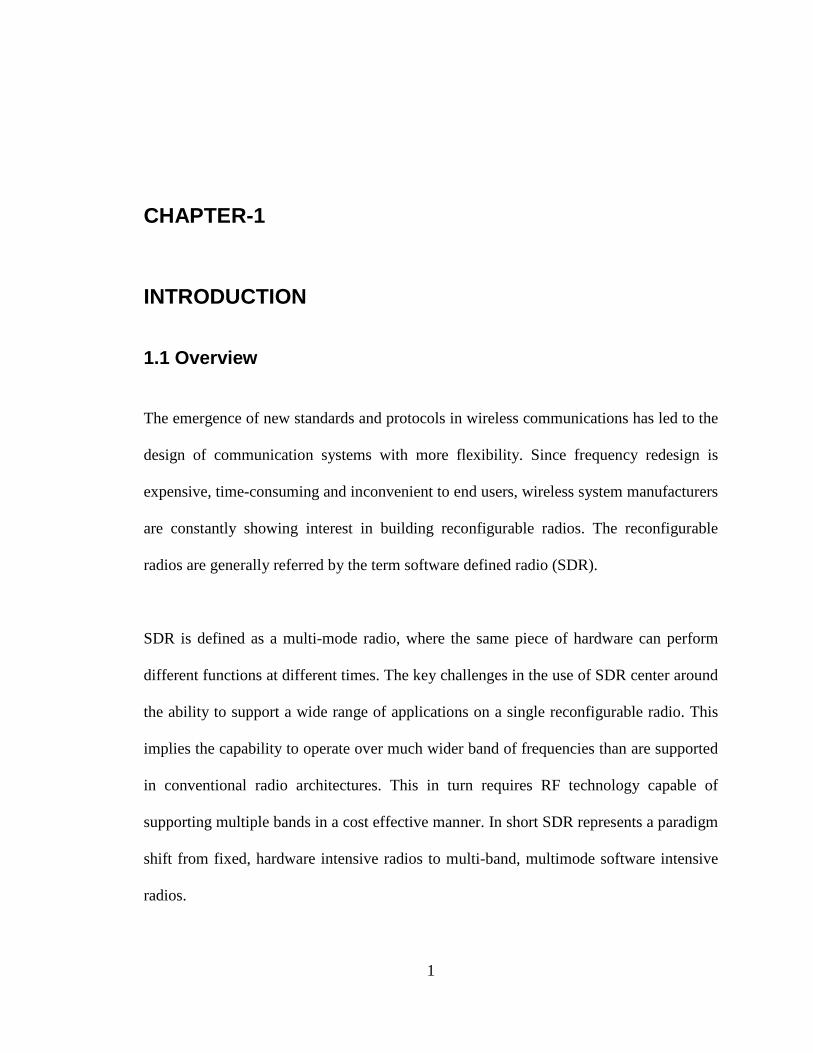
INTRODUCTION
1.1 Overview
The emergence of new standards and protocols in wireless communications has led to the
design of communication systems with more flexibility. Since frequency redesign is
expensive, time-consuming and inconvenient to end users, wireless system manufacturers
are constantly showing interest in building reconfigurable radios. The reconfigurable
radios are generally referred by the term software defined radio (SDR).
SDR is defined as a multi-mode radio, where the same piece of hardware can perform
different functions at different times. The key challenges in the use of SDR center around
the ability to support a wide range of applications on a single reconfigurable radio. This
implies the capability to operate over much wider band of frequencies than are supported
in conventional radio architectures. This in turn requires RF technology capable of
supporting multiple bands in a cost effective manner. In short SDR represents a paradigm
shift from fixed, hardware intensive radios to multi-band, multimode software intensive
radios.

2
The RF front end in the SDR should incorporate simultaneous flexibility in selection of
various constraints, such as centre frequency, power gain, bandwidth etc. There will be
tradeoff in achieving the flexibility and satisfying the constraints. However using a
software radio design, it is possible to compensate for some of the inadequacies of the RF
components in digital domain.
The goal of this thesis is to build a generic reconfigurable RF receiver where each part of
the receiver is dynamically reconfigured through the software. In this respect, the design
of reconfigurable filter, Low noise amplifier, Oscillator and a Power amplifier is
discussed. Although the main aim is to reconfigure the circuits as much as possible, care
is taken such that the performance metrics of the circuits is not traded off too much.
1.2 Organization of Thesis
The thesis is organized into five chapters. Chapter 2 deals with the design procedure of
reconfigurable low noise amplifier, Chapter 3 focuses on the design of reconfigurable
switching matrix oscillator. Chapter 4 deals with design of reconfigurable power
amplifier and chapter 5 introduces the concept of reconfigurable filter. The simulation
results are discussed at the end of each chapter. The conclusions and future work are
discussed in chapter 6. Simulations of the circuits are conducted by using Cadence
spectreRF in CMOS 0.5um peregrine process.
3
CHAPTER 2-
RECONFIGURABLE LOW NOISE AMPLIFIER
The diverse range of modern wireless applications necessitates communication systems
with more bandwidth and flexibility. In order to increase flexibility on the market and the
functionality of RF transceivers, RF designers are pursuing solutions for cost effective
multi standard transceivers. The feasibility of a multi standard transceiver is greatly
influenced by the feasibility of a multi band LNA. Therefore in this chapter, the design of
a non-concurrent dual band low noise amplifier is presented that is capable of operating
at two different frequencies without significantly changing the performance metrics.
2.1 Low Noise Amplifier
The low noise amplifier is typically the first stage of a receiver, whose main function is to
provide enough gain to overcome the noise of subsequent stages. The LNA should
accommodate large signals without distortion and frequently must also present specific
impedance, such as 50Ω , to the input source.
The difficulty in the design of a multi band LNA comes from the fact that it has to
provide functions as input matching at different frequencies, adaptivity in order to satisfy
different set of specifications like low noise figure(NF), high gain and good linearity.
4
These specifications depend on the set design parameters in a way that improvement of
one will deteriorate the others.
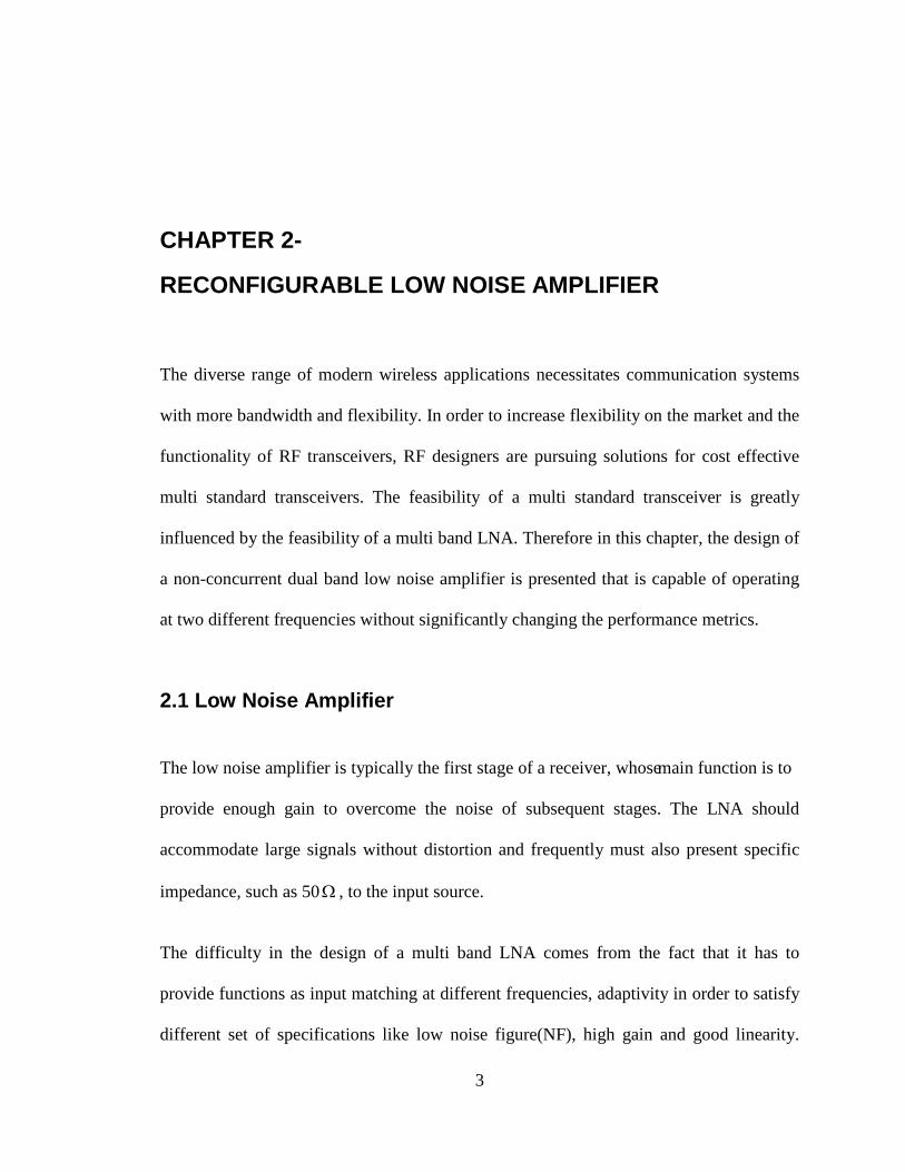
2.1.1 Topology Selection:
The first step in the design of a low noise amplifier is the topology selection. One
possibility is to use the common gate stage (Fig. 2.1) in order to realize the wide band
LNA. The advantage of this approach is that the input impedance is equal to 1/gm, where
gm is the transconductance of the MOS transistor, but the disadvantage is rather high
minimum NF of 2.2 dB [1].
Fig 2.1 Common Gate Amplifier Fig 2.2 Common source amplifier with shunt input resistor.
Another straightforward approach is to provide a reasonably broadband 50-Ωtermination by simply keeping a 50-Ω resistor across the input terminals of a common
source amplifier (Fig. 2.2). Unfortunately, the resistor adds the thermal noise of its own
and the signal will be attenuated by a factor of 2 ahead of the transistor.
5
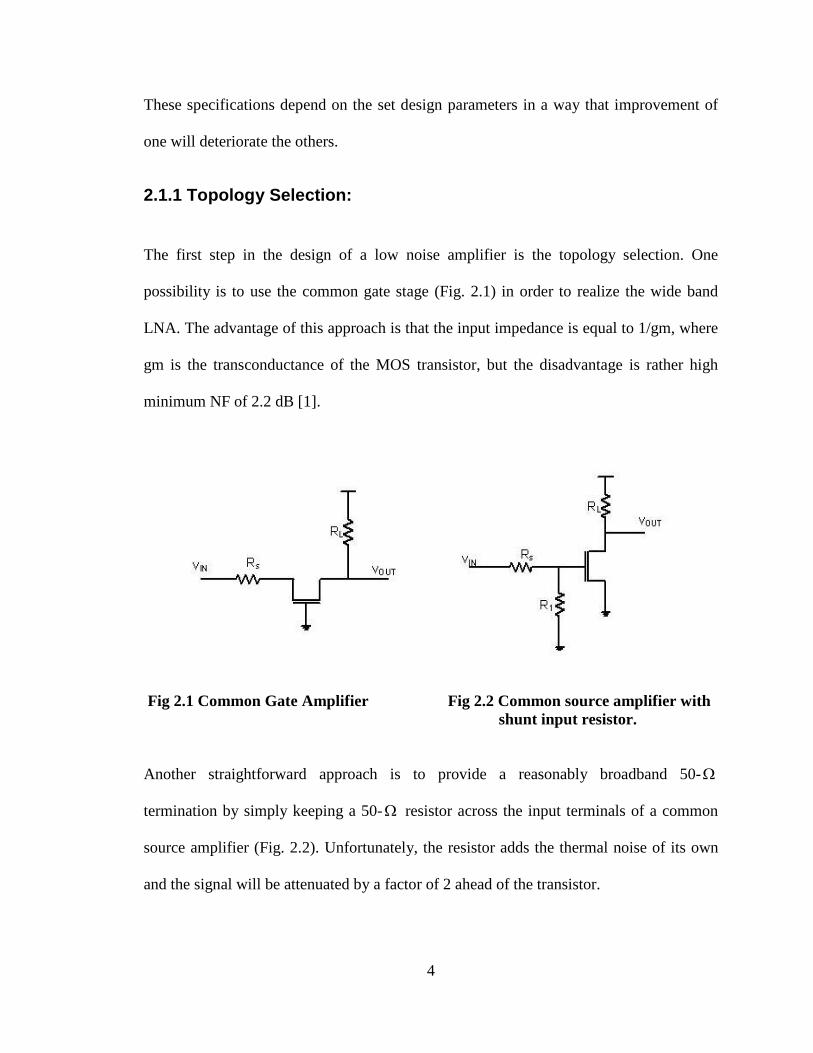
Fig 2.3 Shunt-series amplifier
The shunt-series amplifier (Fig. 2.3) is another circuit that provides broadband real input
impedance. The noise figure of this circuit is better than the circuit described above as its
does not reduce the signal with a noisy attenuator, yet the feedback circuit network
continues to generate thermal noise of its own and also fails to present to transistor an
optimal impedance at all frequencies.
Another method is to employ inductive source degeneration (Fig. 2.4). The important
advantage of this method is that one can control the real part of the input impedance
through proper choice of inductance.
6
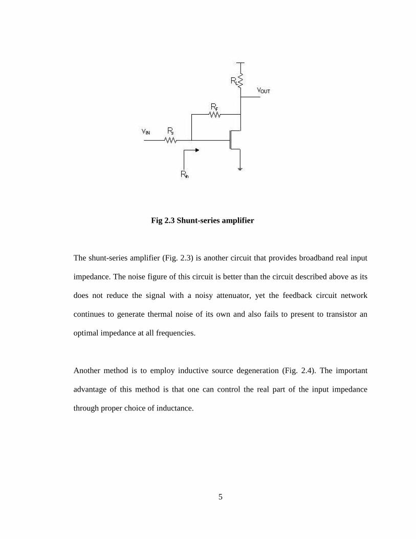
2.2 Inductive source de-generated low noise amplifier:
2.2.1 Input Impedance Match
The input impedance matching is very important in LNA design. Impedance matching
using inductive source degeneration is a very popular approach because matching to the
source does not introduce additional noise (as opposed to the case of using a shunt input
resistor), and does not restrict the value of gm as in the case of the common gate
configuration.
Fig 2.4 Narrow band LNA with inductive source degeneration.
The input impedance of the above circuit is given by
1( ) ( ) m
in s g sgs gs
gZ s s L L L
sC C= + + + …………… (2.1)
7
For power match at the input, the input impedance should be real which is equal
to ms
gs
gL
C. Hence the resonant frequency is
1
( )o
g s gsL L Cω =
+ …………… (2.2)
2.2.2 Load Circuit:
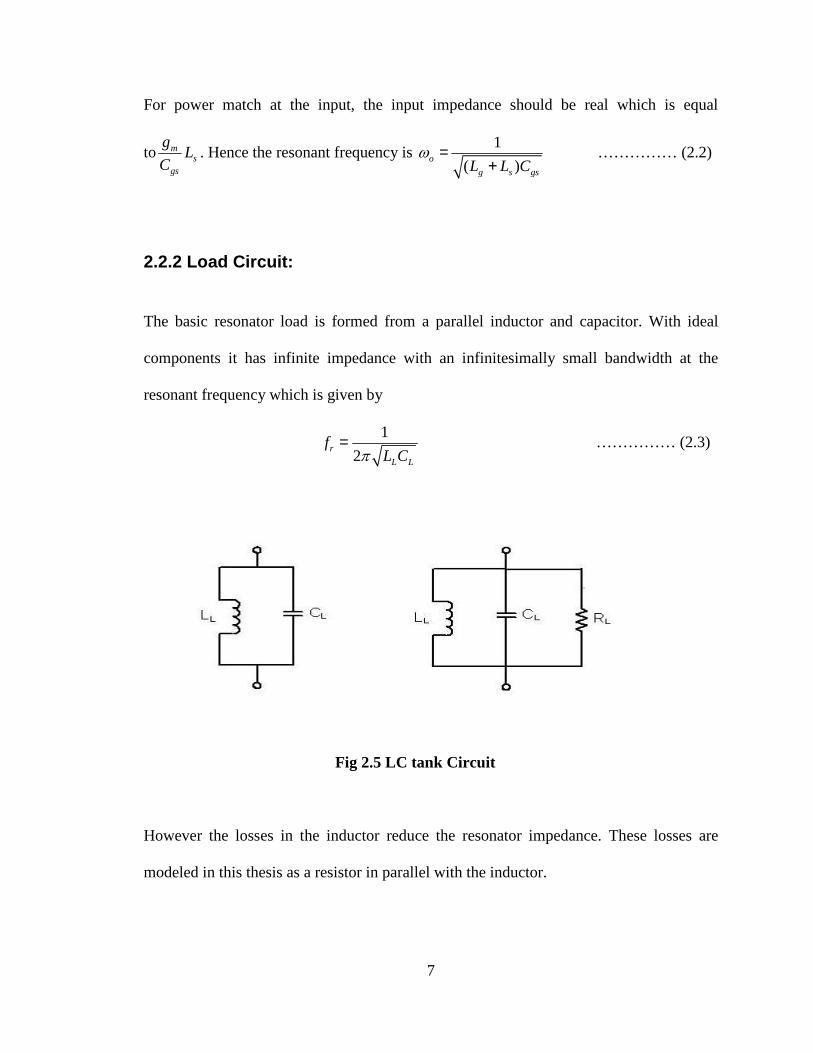
The basic resonator load is formed from a parallel inductor and capacitor. With ideal
components it has infinite impedance with an infinitesimally small bandwidth at the
resonant frequency which is given by
1
2r
L L
fL Cπ= …………… (2.3)
Fig 2.5 LC tank Circuit
However the losses in the inductor reduce the resonator impedance. These losses are
modeled in this thesis as a resistor in parallel with the inductor.

8
2.2.3 Voltage Gain
The voltage gain of the inductively degenerated amplifier is given by
| | ( )mGain g Z j Qω= …………… (2.4)
where gm is the transconductance of the input transistor, ( )Z jω is the load impedance of
the LNA and Q is the quality factor of the input matching network.
At resonance the load impedance becomes a real quantity ( LR ) and is used to set the
desired gain. The higher the value of LR , the higher will be the quality factor of the load
circuit. Generally the value of LR is set according to overall receiver noise and IIP3
requirements.
2.2.4 Noise Figure
The noise figure determines how much the LNA (or any device) degrades the signal to
noise ratio. Before beginning an analysis of how to reduce the noise figure, the origins of
noise must be identified and understood. This section gives insight into the important
noise sources in CMOS transistors.
Thermal noise: Thermal noise is due to the random thermal motion of the carriers in the
channel. The thermally agitated carriers in the channel cause a randomly varying current
and the current is given by
_2 4 do
ndi kT g fγ= ∆ …………… (2.5)
9
whereγ is called excess noise factor and is typically 2/3 in long channel and 2 or 3 in
short channel devices. dog is defined as channel conductance with 0dsV = .
( )ddo n ox gs T
ds
dI Wg C V V
dV Lµ⇒ = = − …………… (2.6)
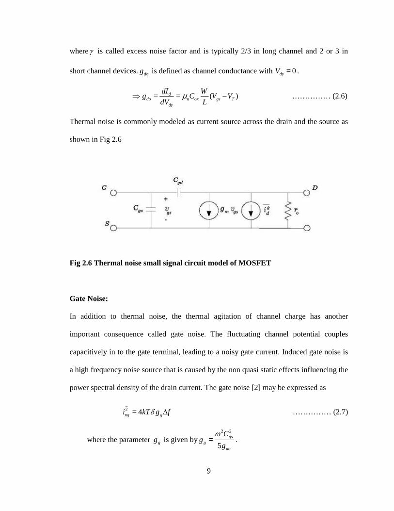
Thermal noise is commonly modeled as current source across the drain and the source as
shown in Fig 2.6
Fig 2.6 Thermal noise small signal circuit model of MOSFET
Gate Noise:
In addition to thermal noise, the thermal agitation of channel charge has another
important consequence called gate noise. The fluctuating channel potential couples
capacitively in to the gate terminal, leading to a noisy gate current. Induced gate noise is
a high frequency noise source that is caused by the non quasi static effects influencing the
power spectral density of the drain current. The gate noise [2] may be expressed as
_2 4ng gi kT g fδ= ∆ …………… (2.7)
where the parameter gg is given by2 2
5gs
gdo
Cg
g
ω= .
10
The value of the parameter is equal to 4/3 in long channel devices [1]. Since thermal
channel noise and induced gate noise stem from the same physical phenomenon, [2]
assumes that the relation 2δ γ= continues to hold for short channel devices.
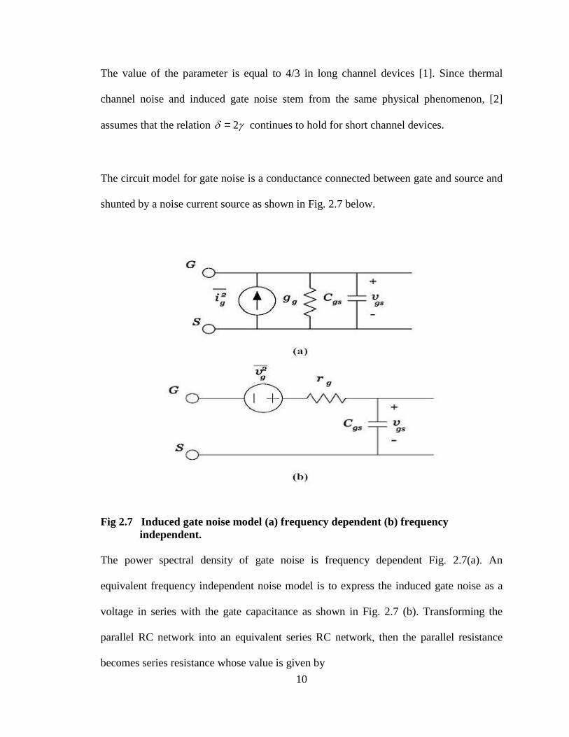
The circuit model for gate noise is a conductance connected between gate and source and
shunted by a noise current source as shown in Fig. 2.7 below.
Fig 2.7 Induced gate noise model (a) frequency dependent (b) frequencyindependent.
The power spectral density of gate noise is frequency dependent Fig. 2.7(a). An
equivalent frequency independent noise model is to express the induced gate noise as a
voltage in series with the gate capacitance as shown in Fig. 2.7 (b). Transforming the
parallel RC network into an equivalent series RC network, then the parallel resistance
becomes series resistance whose value is given by
11
2
1 1 1.
1 5gg do
rg Q g
= ≈+
, which is independent of frequency.
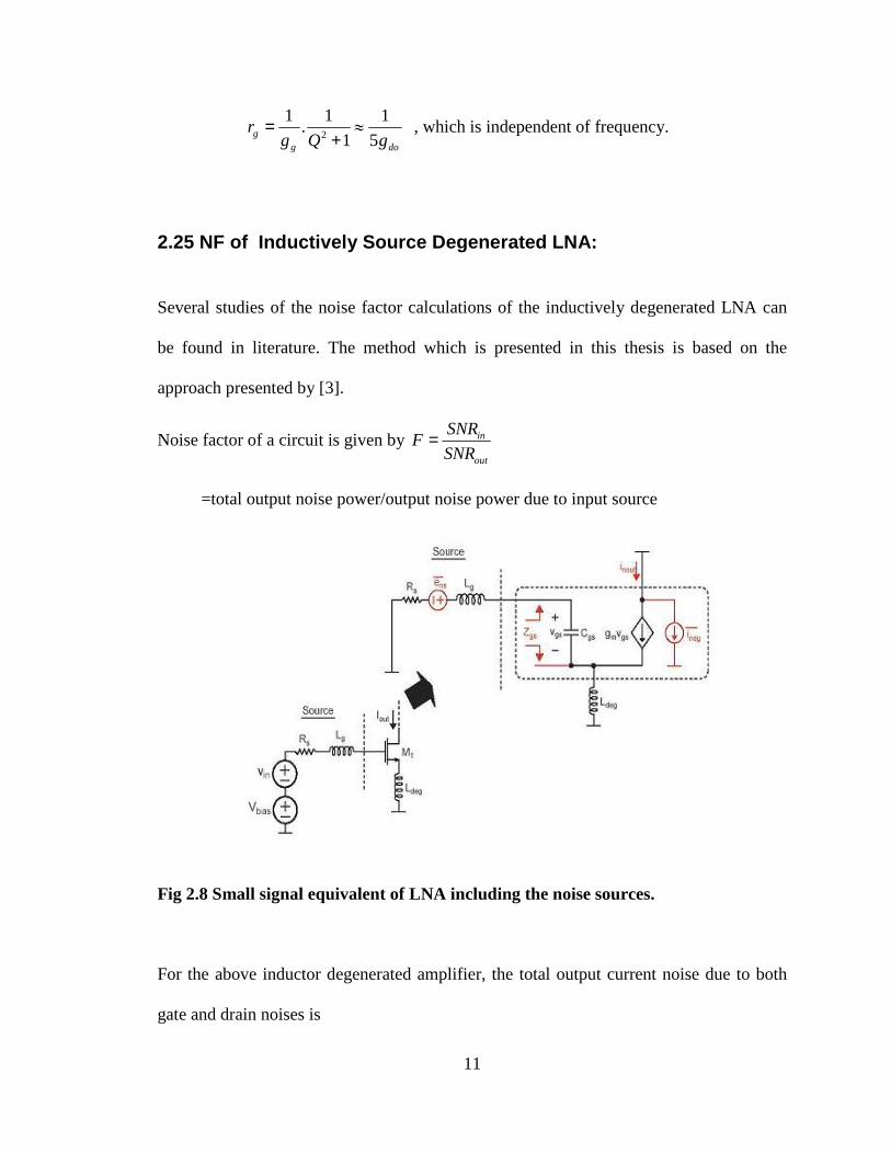
2.25 NF of Inductively Source Degenerated LNA:
Several studies of the noise factor calculations of the inductively degenerated LNA can
be found in literature. The method which is presented in this thesis is based on the
approach presented by [3].
Noise factor of a circuit is given by in
out
SNRF
SNR=
=total output noise power/output noise power due to input source
Fig 2.8 Small signal equivalent of LNA including the noise sources.
For the above inductor degenerated amplifier, the total output current noise due to both
gate and drain noises is
12
_ _2 2
2 2(1 2 ( 1))ndg ndgd d
i ic Q
f fχ χ= − + +∆ ∆ …………… (2.8)
where c is the correlation factor between gate and drain noise, 5
md
do
g
g
δχ γ= and Q is
the quality factor of the input resonant circuit.
Output noise due to source resistance_
2 2( ) 4nout m si g Q kTR f= ∆
Finally substituting the values for the noise sources, the noise factor is given by
( )2 20 11 1 2 (4 1)
2do
d dt m
gc Q
g Q
ω γ χ χω
= + − + + …………… (2.9)
2.2.6 Linearity
A low noise amplifier is often included in a receiver circuit to provide sufficient gain to
overcome the noise in subsequent stages. Apart form providing enough gain, the LNA
must also provide good linearity and a wide usable dynamic range. The LNA must
maintain linear operation in the presence of strong interfering one.
Due to inherent non linearity present in the input MOS device of LNA, the interference
effects involving one or more undesired output signals results in distortion or non
linearity of the output signal.
13
There are various ways to describe the linearity of a system. The linearity of LNA is
generally determined by a common measure called input third order Interception point or
input IIP3.
The output of the LNA can be described by a power series of the form
2 30 1 2 3( ) ( ) ( ) ( ) ..........y t c c x t c x t c x t= + + + +
where ( )x t is the input to the system.
Assume that the input to the system is a sum of two sinusoidal signals with frequency
components of 1ω and 2ω , having amplitude of A. The fundamental component is given
by [ ]31 3 1 2
3cos( ) cos( )
4c A c A t tω ω + + [ ]3
1 3 1 2
3cos( ) cos( )
4c A c A t tω ω + + while the third
order intermodulation term gives the
sum [ ]33 1 1 1 1 1 2 1 2
3cos( 2 ) cos( 2 ) cos(2 ) cos(2 )
4c A t t t tω ω ω ω ω ω ω ω+ + − + + + − . The sum of
frequency terms can be neglected in the above term. The IIP3 of the amplifier can be
determined by equating the fundamental amplitude and the third order product amplitude.

14
Fig 2.9 Illustration of LNA linearity parameters.
15
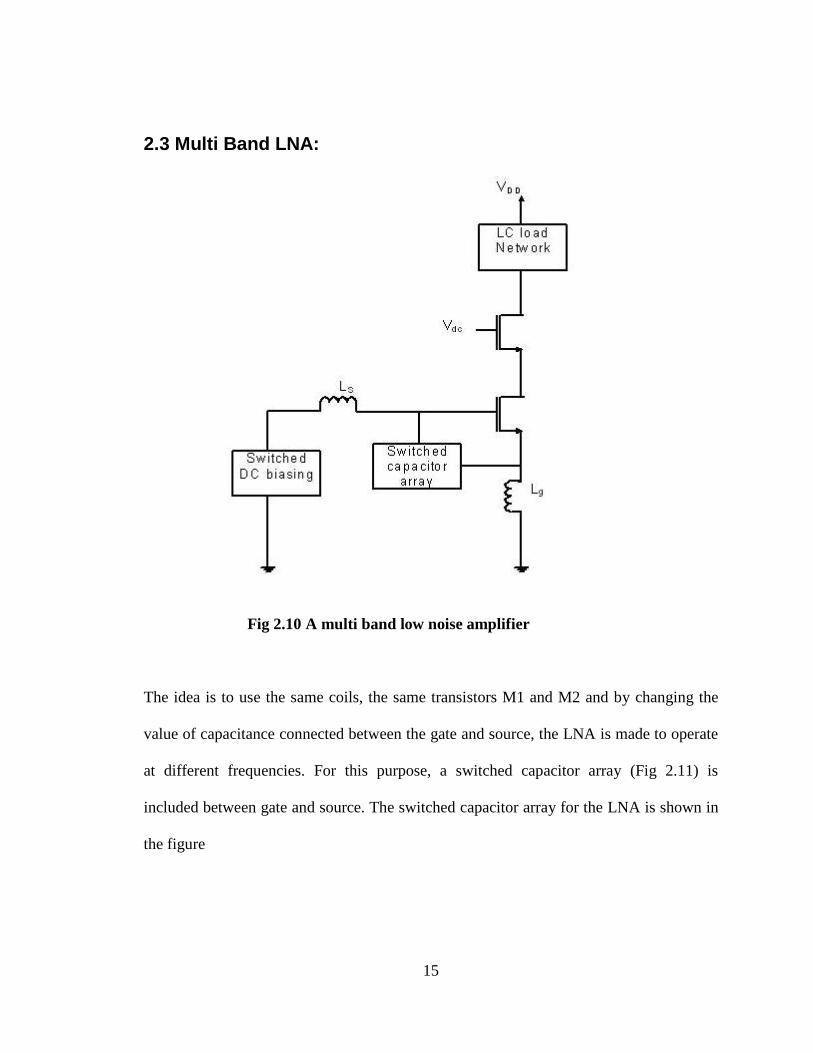
2.3 Multi Band LNA:
Fig 2.10 A multi band low noise amplifier
The idea is to use the same coils, the same transistors M1 and M2 and by changing the
value of capacitance connected between the gate and source, the LNA is made to operate
at different frequencies. For this purpose, a switched capacitor array (Fig 2.11) is
included between gate and source. The switched capacitor array for the LNA is shown in
the figure

16
Fig 2.11 Switched capacitor array for LNA
As an example, consider the dual band low noise amplifier as shown in the Fig. 2.12
Fig 2.12 A dual band low noise amplifier
17
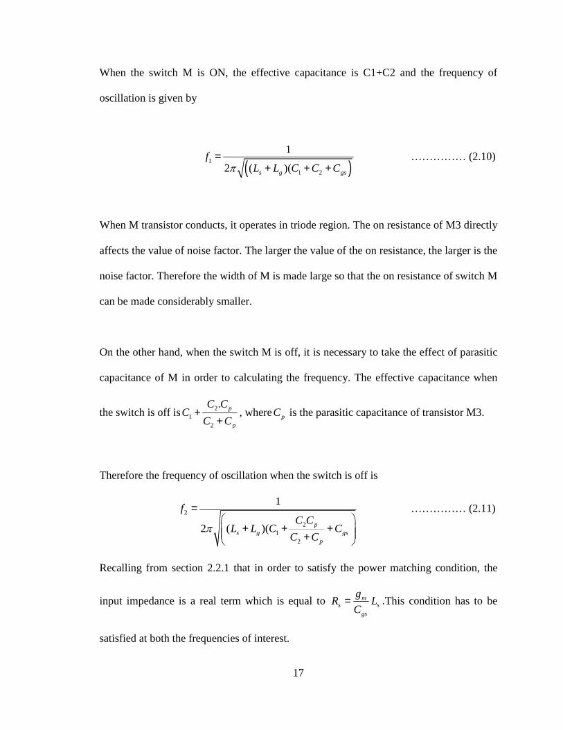
When the switch M is ON, the effective capacitance is C1+C2 and the frequency of
oscillation is given by
( )1
1 2
1
2 ( )(s g gs
fL L C C Cπ=
+ + + …………… (2.10)
When M transistor conducts, it operates in triode region. The on resistance of M3 directly
affects the value of noise factor. The larger the value of the on resistance, the larger is the
noise factor. Therefore the width of M is made large so that the on resistance of switch M
can be made considerably smaller.
On the other hand, when the switch M is off, it is necessary to take the effect of parasitic
capacitance of M in order to calculating the frequency. The effective capacitance when
the switch is off is 21
2
. p
p
C CC
C C+
+, where pC is the parasitic capacitance of transistor M3.
Therefore the frequency of oscillation when the switch is off is
2
21
2
1
2 ( )( ps g gs
p
fC C
L L C CC C
π=
+ + + +
…………… (2.11)
Recalling from section 2.2.1 that in order to satisfy the power matching condition, the
input impedance is a real term which is equal to ms s
gs
gR L
C= .This condition has to be
satisfied at both the frequencies of interest.
18
1 2
1 2
m m
gs gs
g g
C C=
2
1 2
2 1
m
m
g f
g f
⇒ = …………… (2.12)
The transconductance of the Mosfet can be changed by dynamically adjusting its bias
voltage using a switch as shown in Fig. 2.12
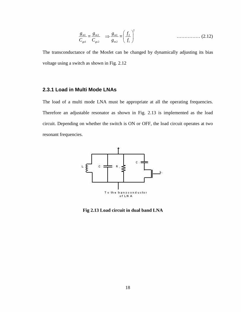
2.3.1 Load in Multi Mode LNAs
The load of a multi mode LNA must be appropriate at all the operating frequencies.
Therefore an adjustable resonator as shown in Fig. 2.13 is implemented as the load
circuit. Depending on whether the switch is ON or OFF, the load circuit operates at two
resonant frequencies.
Fig 2.13 Load circuit in dual band LNA

19
2.4 Results of Reconfigurable LNA
Fig 2.14: Schematic of Reconfigurable LNA.
The above shown LNA can be reconfigured to one of the dual bands by switching the
digital input to the gate of MOSFET M7. In order to be compatible to DECT and GSM
standards, the LNA has been designed to operate at frequencies of 1.9 GHz and 2.4 GHz.
The noise figure degraded from 2.1 to 3.6 when the LNA is reconfigured. This is due to
noise contributed by the mosfet M7 when it is turned on. Also the gain decreases which
can be adjusted by using a switched tuned circuit at the load.
20
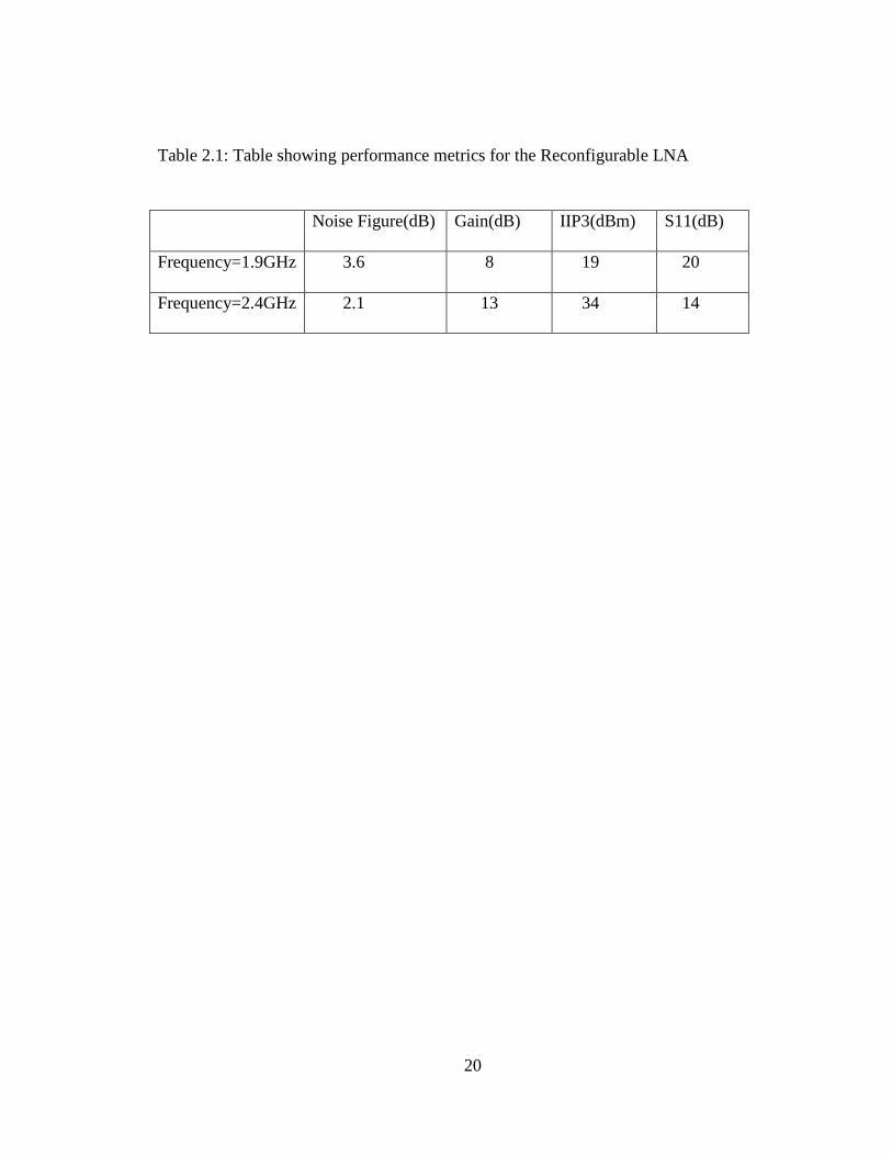
Table 2.1: Table showing performance metrics for the Reconfigurable LNA
Noise Figure(dB) Gain(dB) IIP3(dBm) S11(dB)
Frequency=1.9GHz 3.6 8 19 20
Frequency=2.4GHz 2.1 13 34 14
21
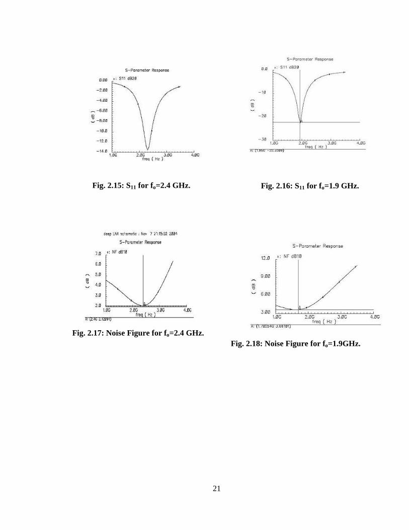
Fig. 2.15: S11 for fo=2.4 GHz.
Fig. 2.17: Noise Figure for fo=2.4 GHz.
Fig. 2.16: S11 for fo=1.9 GHz.
Fig. 2.18: Noise Figure for fo=1.9GHz.

22
Fig. 2.19: S21 for fo=1.9 GHz.
Fig. 2.21: IIP3 for fo=2.4 GHz.
Fig. 2.20: S21 for fo=2.4 GHz.
Fig. 2.22: IIP3 for fo=1.9 GHz.
23
CHAPTER 3-
Reconfigurable Negative Resistance LC Oscillator
In this chapter, a new way for obtaining different oscillation frequencies using a negative
resistance oscillator is discussed. Also the concepts which are vital in understanding how
the negative resistance LC tuned oscillator works are discussed.
3.1 Choosing an Oscillator Architecture
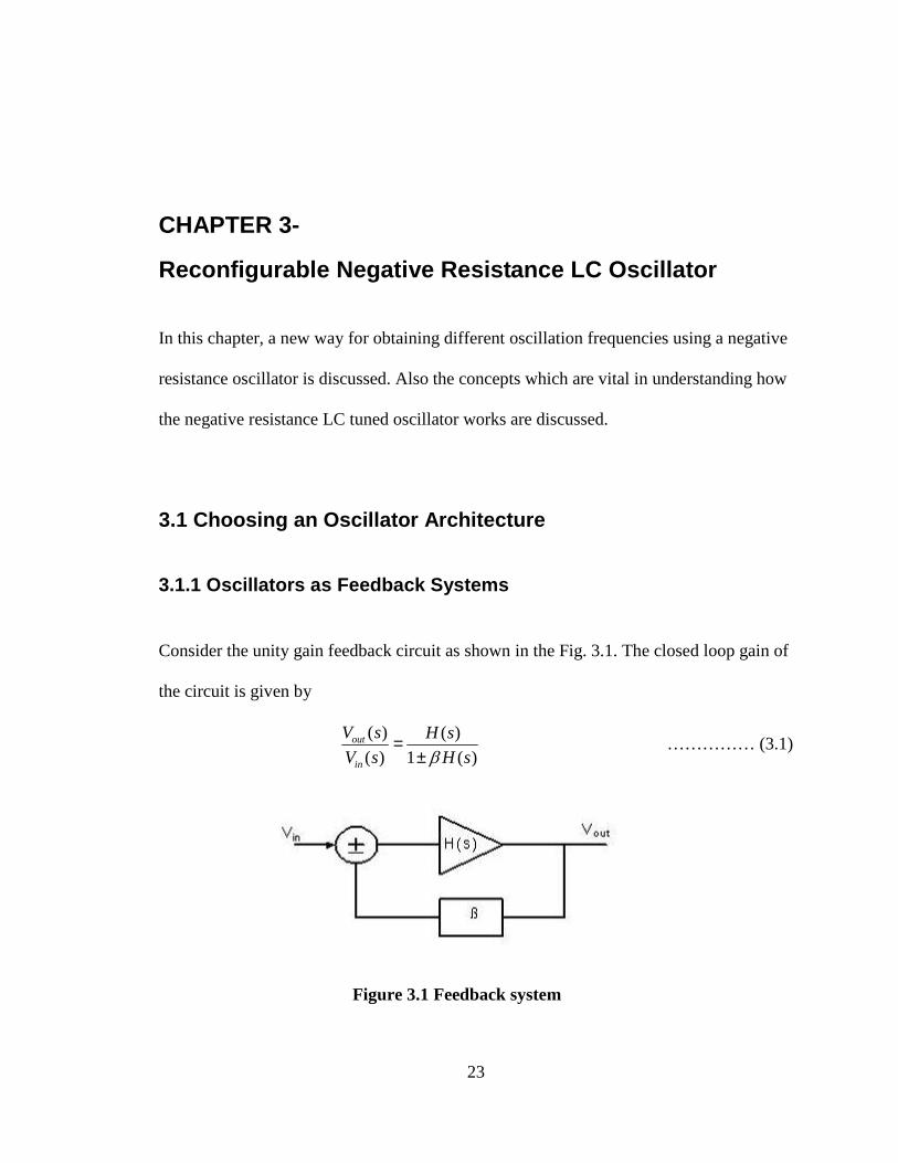
3.1.1 Oscillators as Feedback Systems
Consider the unity gain feedback circuit as shown in the Fig. 3.1. The closed loop gain of
the circuit is given by
( ) ( )
( ) 1 ( )out
in
V s H s
V s H sβ=±
…………… (3.1)
Figure 3.1 Feedback system
24
If the loop gain ( ) 1oH jβ ω = − , then the closed loop gain goes to infinity at oω . Under
this condition the circuit amplifies its own noise components at oω indefinitely. In theory,
the oscillation amplitude grows to infinity at this frequency. However in practice, due to
inherent non linearity present in the system, larger amplitude lowers the loop gain, which
eventually establishes a stable condition with constant oscillation amplitude. The
condition ( ( ) 1H sβ = − ) is known as Barkhausen’s criteria.
In summary, if a negative feedback has a loop gain that satisfies two conditions at oω ω=
( ) 1H sβ = …………… (3.2)
( ) 180oH sβ∠ =
then the circuit may oscillate at oω .
There are different ways in realizing the negative feedback systems that satisfy the
Barkhausen’s criteria. For fully integrated CMOS oscillators, two common approaches
are ring oscillators and LC oscillators. In this report we will focus on LC oscillators as it
forms the core of the structure to be presented later.
25
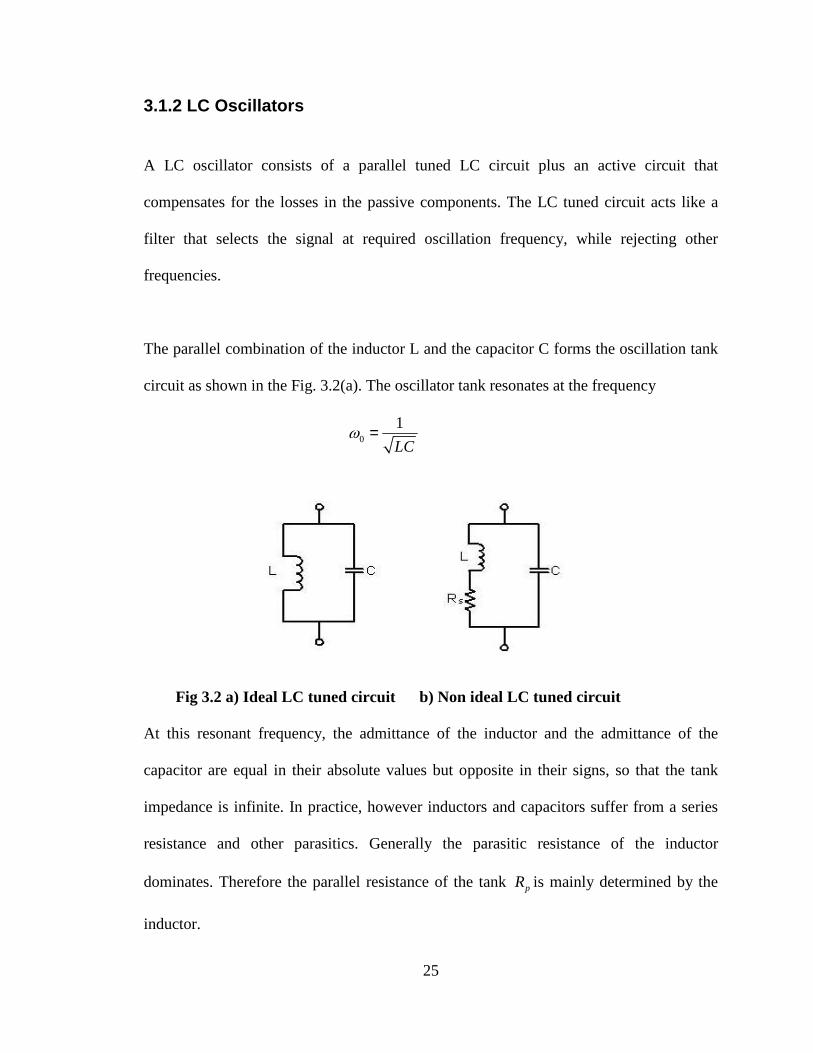
3.1.2 LC Oscillators
A LC oscillator consists of a parallel tuned LC circuit plus an active circuit that
compensates for the losses in the passive components. The LC tuned circuit acts like a
filter that selects the signal at required oscillation frequency, while rejecting other
frequencies.
The parallel combination of the inductor L and the capacitor C forms the oscillation tank
circuit as shown in the Fig. 3.2(a). The oscillator tank resonates at the frequency
0
1
LCω =
Fig 3.2 a) Ideal LC tuned circuit b) Non ideal LC tuned circuit
At this resonant frequency, the admittance of the inductor and the admittance of the
capacitor are equal in their absolute values but opposite in their signs, so that the tank
impedance is infinite. In practice, however inductors and capacitors suffer from a series
resistance and other parasitics. Generally the parasitic resistance of the inductor
dominates. Therefore the parallel resistance of the tank pR is mainly determined by the
inductor.
26
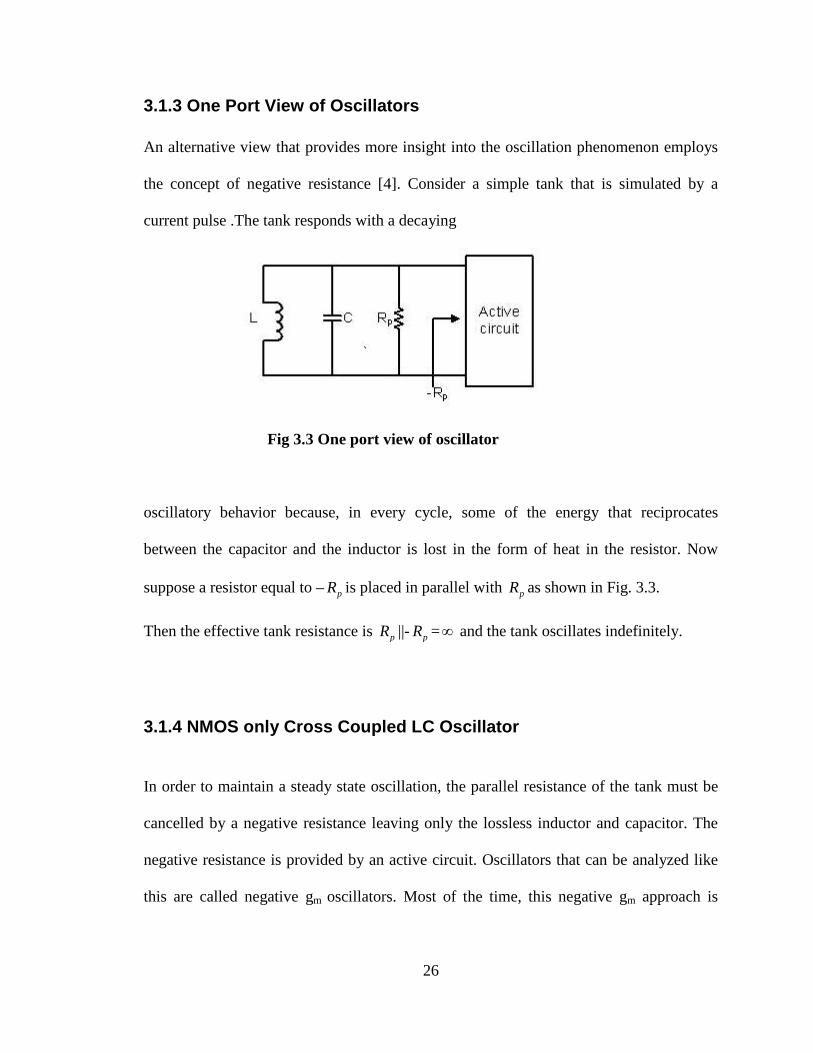
3.1.3 One Port View of Oscillators
An alternative view that provides more insight into the oscillation phenomenon employs
the concept of negative resistance [4]. Consider a simple tank that is simulated by a
current pulse .The tank responds with a decaying
Fig 3.3 One port view of oscillator
oscillatory behavior because, in every cycle, some of the energy that reciprocates
between the capacitor and the inductor is lost in the form of heat in the resistor. Now
suppose a resistor equal to – pR is placed in parallel with pR as shown in Fig. 3.3.
Then the effective tank resistance is pR ||- pR =∞ and the tank oscillates indefinitely.
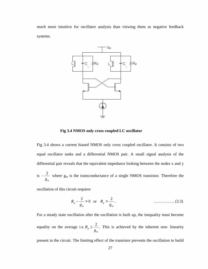
3.1.4 NMOS only Cross Coupled LC Oscillator
In order to maintain a steady state oscillation, the parallel resistance of the tank must be
cancelled by a negative resistance leaving only the lossless inductor and capacitor. The
negative resistance is provided by an active circuit. Oscillators that can be analyzed like
this are called negative gm oscillators. Most of the time, this negative gm approach is
27
much more intuitive for oscillator analysis than viewing them as negative feedback
systems.
Fig 3.4 NMOS only cross coupled LC oscillator
Fig 3.4 shows a current biased NMOS only cross coupled oscillator. It consists of two
equal oscillator tanks and a differential NMOS pair. A small signal analysis of the
differential pair reveals that the equivalent impedance looking between the nodes x and y
is 2
mg− where gm is the transconductance of a single NMOS transistor. Therefore the
oscillation of this circuit requires
20p
m
Rg
− > or2
pm
Rg
> . …………… (3.3)
For a steady state oscillation after the oscillation is built up, the inequality must become
equality on the average i.e.2
pm
Rg
≥ . This is achieved by the inherent non- linearity
present in the circuit. The limiting effect of the transistor prevents the oscillation to build
28
up continuously. Asserting oscillation start up is the most crucial part in oscillator design,
because pR is generally not accurately known. Generally the transconductances of the
transistors will be three or four times larger than the required by the design criteria.
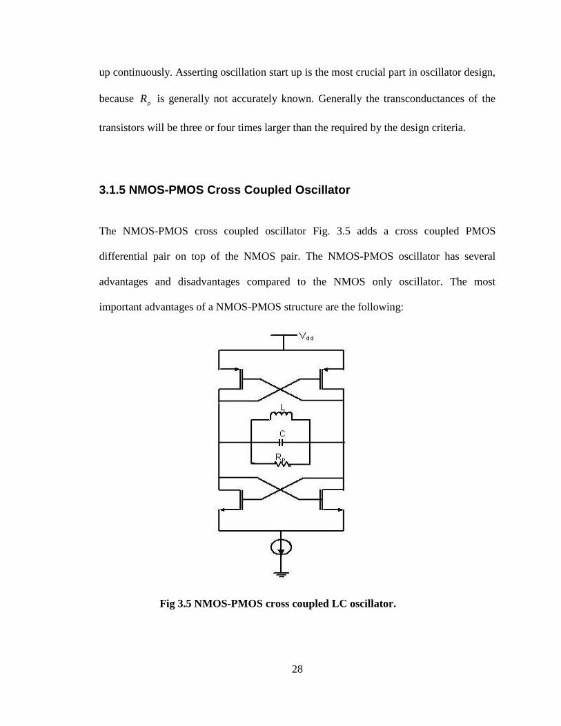
3.1.5 NMOS-PMOS Cross Coupled Oscillator
The NMOS-PMOS cross coupled oscillator Fig. 3.5 adds a cross coupled PMOS
differential pair on top of the NMOS pair. The NMOS-PMOS oscillator has several
advantages and disadvantages compared to the NMOS only oscillator. The most
important advantages of a NMOS-PMOS structure are the following:
Fig 3.5 NMOS-PMOS cross coupled LC oscillator.
29
Less power consumption For a given bias current, the NMOS-PMOS structure attains
a negative admittance of ( ) / 2mn mpg g− + where mng is the transconductance of NMOS
transistor and mpg is that of PMOS transistor. For the same bias current, the NMOS only
structure attains a negative admittance of2mg− . With the addition of PMOS transistors, it
becomes possible to compensate for the loss in the LC tank with a lower bias current than
in a NMOS-only structure.
Smaller 1/∆f3 noise corner If the transconductances of PMOS and NMOS transistors
are made equal, then it is possible to obtain a symmetric oscillation waveform at the
outputs compared to the NMOS only structure. This better rise and fall symmetry reduces
the up conversion of transistor 1/∆f flicker noise [6]. Therefore NMOS-PMOS structures
attain a smaller 1/∆f3 noise corner in the phase noise characteristic than NMOS only
structure.
The NMOS-PMOS structure also has drawbacks over the NMOS only structure. The
most important ones are
Increased parasitic capacitance The addition of PMOS transistors contributes a
significant amount of parasitic capacitance. The parasitic capacitance contributed by the
PMOS pair can be two to three times greater than the NMOS pair. The larger the parasitic
or constant capacitance, lower the tuning range. However, by adding the PMOS
30
transistors the width of the NMOS transistors can be decreased to achieve the same gain
compared to the NMOS only structure, thereby mitigating the problem to some extent.
Reduced output swing In the NMOS-PMOS structure, the steady state voltage at the
output settle somewhere between 0V and Vdd. The maximum differential output voltage
will be larger for the NMOS only structure than the NMOS-PMOS structure. However
the fact that the oscillation in the NMOS only structure takes place around the supply
voltage Vdd may raise the question whether or not this is desirable due to the breakdown
effects at the oscillation peaks. Despite these concerns NMOS only structure is a good
option at low supply voltages.
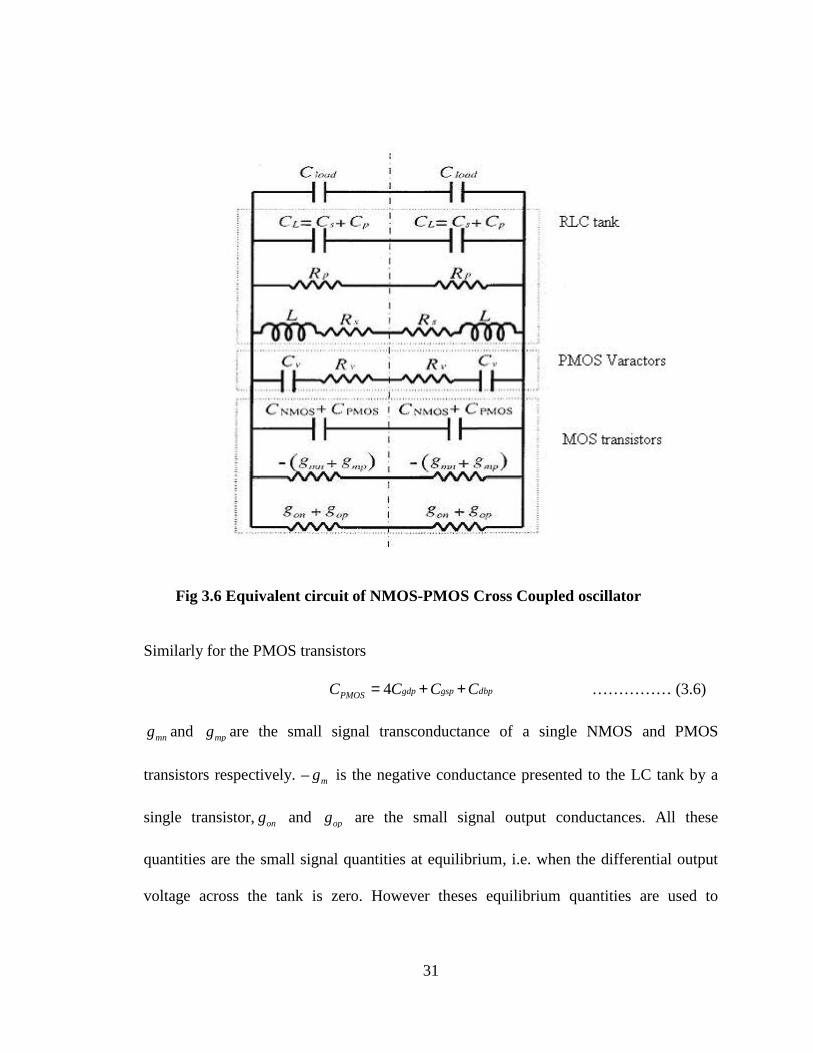
3.1.6 Analysis of NMOS-PMOS LC VCO
As the NMOS-PMOS cross coupled structure forms the core of the oscillator presented in
this report, let us analyze its small signal equivalent circuit and its parameters. Assume an
ideal inductor is used in the circuit. The resulting small signal equivalent circuit of the
VCO core is depicted in Fig. 3.6. CNMOS and CPMOS model the parasitic capacitances of a
single NMOS and PMOS transistor respectively. The parasitic capacitance of a NMOS
pair is shown in the circuit. The equivalent capacitance of a NMOS pair between the two
nodes is thus:
1 12
2 2NMOS Pair gdn gsn dbnC C C C− = + + …………… (3.4)
NMOS PairC − is the series combination of two CNMOS and thus
4NMOS gdn gsn dbnC C C C= + + …………… (3.5)
31
Fig 3.6 Equivalent circuit of NMOS-PMOS Cross Coupled oscillator
Similarly for the PMOS transistors
4 gdp gsp dbpPMOSC C C C= + + …………… (3.6)
mng and mpg are the small signal transconductance of a single NMOS and PMOS
transistors respectively. – mg is the negative conductance presented to the LC tank by a
single transistor, ong and opg are the small signal output conductances. All these
quantities are the small signal quantities at equilibrium, i.e. when the differential output
voltage across the tank is zero. However theses equilibrium quantities are used to
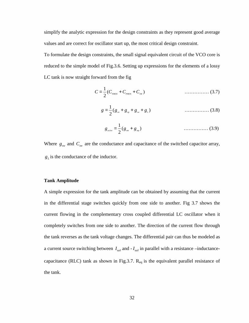
32
simplify the analytic expression for the design constraints as they represent good average
values and are correct for oscillator start up, the most critical design constraint.
To formulate the design constraints, the small signal equivalent circuit of the VCO core is
reduced to the simple model of Fig.3.6. Setting up expressions for the elements of a lossy
LC tank is now straight forward from the fig
1( )
2 NMOS PMOS SWC C C C= + + …………… (3.7)
1( )
2 on op sw Lg g g g g= + + + …………… (3.8)
1( )
2active mn mpg g g= + …………… (3.9)
Where swg and swC are the conductance and capacitance of the switched capacitor array,
Lg is the conductance of the inductor.
Tank Amplitude
A simple expression for the tank amplitude can be obtained by assuming that the current
in the differential stage switches quickly from one side to another. Fig 3.7 shows the
current flowing in the complementary cross coupled differential LC oscillator when it
completely switches from one side to another. The direction of the current flow through
the tank reverses as the tank voltage changes. The differential pair can thus be modeled as
a current source switching between tailI and - tailI in parallel with a resistance –inductance-
capacitance (RLC) tank as shown in Fig.3.7. Req is the equivalent parallel resistance of
the tank.
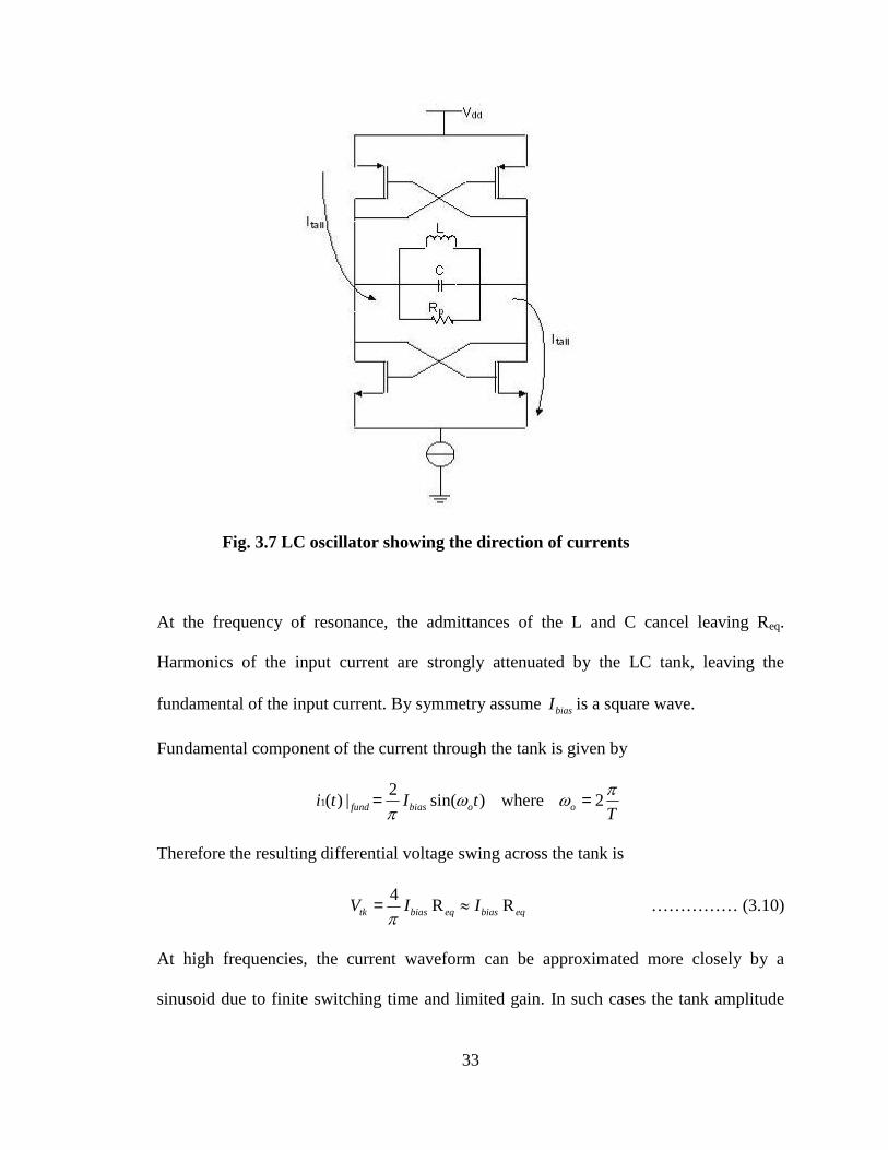
33
Fig. 3.7 LC oscillator showing the direction of currents
At the frequency of resonance, the admittances of the L and C cancel leaving Req.
Harmonics of the input current are strongly attenuated by the LC tank, leaving the
fundamental of the input current. By symmetry assume biasI is a square wave.
Fundamental component of the current through the tank is given by
12
( ) | sin( )fund bias oi t I tωπ= where 2o T
πω =
Therefore the resulting differential voltage swing across the tank is
4R Rtk bias eq bias eqV I Iπ= ≈ …………… (3.10)
At high frequencies, the current waveform can be approximated more closely by a
sinusoid due to finite switching time and limited gain. In such cases the tank amplitude
34
can be better approximated as Rtk bias eqV I= . This mode of operation is referred to as
current limited region [6] of operation, since in this regime the tank amplitude is solely
determined by the tail current source and the tank equivalent resistance.
The equation Rtk bias eqV I= loses its validity as the amplitude approaches half of the
supply voltage because both the NMOS and PMOS pairs will enter the triode region at
the peaks of the voltage. Also the tail transistor may spend most (or even all) of its time
in linear region. The tank voltage will be clipped at Vdd by the PMOS transistors and at
ground by the NMOS transistors. Therefore for the complementary cross coupled
oscillator, the tank amplitude does not exceed Vdd. Note that since the tail transistor
operates in the triode region for some time, the tail current does not stay constant. Thus
the drain source voltage of the differential NMOS transistors can drop significantly,
resulting in a large drop in their drain current. This region of operation is known as
voltage limited regime.
3.2 Phase Noise in Oscillators
Phase noise is a measure of uncertainty in the output of the oscillator which defines the
frequency domain uncertainty of an oscillator. The output of an oscillator is generally
given by ( ) cos[ ( )]o ov t V t tω φ= + where ( )tφ gives a measure of phase noise. For small
noise sources, a narrowband modulation approximation can be used to express the
oscillator output as
[ ]( ) cos[ ( )] cos( )cos ( ) sin( )sin ( )o o o o ov t V t t V t t t tω φ ω φ ω φ= + = −

35
[ ]cos( )cos ( ) sin( )sin ( )o o oV t t t tω φ ω φ= −
Therefore the phase noise will be mixed with the carrier to produce the sidebands around
the carrier, giving a direct connection between the phase noise and spectral output of the
oscillator.
Fig. 3.8 Phase noise in LC oscillator
The noise spectral power density of an oscillator is given by
[ ]10 10
( ,1 )( ) 10log 10log ( )sideband o
totalCarrier
P HzL S f
P
ω ωω Φ +∆∆ = =
and the units are
defined as decibels below the carrier per Hertz(dBc/Hz).
The Leeson-Cutler phase noise model predicts the following behavior for the ( )totalL ω∆
3
2
1/2 10log 1 . 1
2fo
s L
FkTL
P Q
ωωω ω ω ∆ ∆ = + + ∆ ∆
…………… (3.11)
36
3.3 Switching Matrix Network
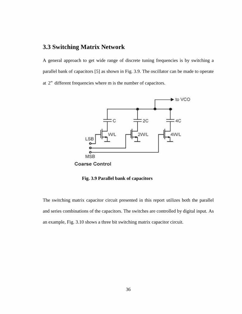
A general approach to get wide range of discrete tuning frequencies is by switching a
parallel bank of capacitors [5] as shown in Fig. 3.9. The oscillator can be made to operate
at 2m different frequencies where m is the number of capacitors.
Fig. 3.9 Parallel bank of capacitors
The switching matrix capacitor circuit presented in this report utilizes both the parallel
and series combinations of the capacitors. The switches are controlled by digital input. As
an example, Fig. 3.10 shows a three bit switching matrix capacitor circuit.
37
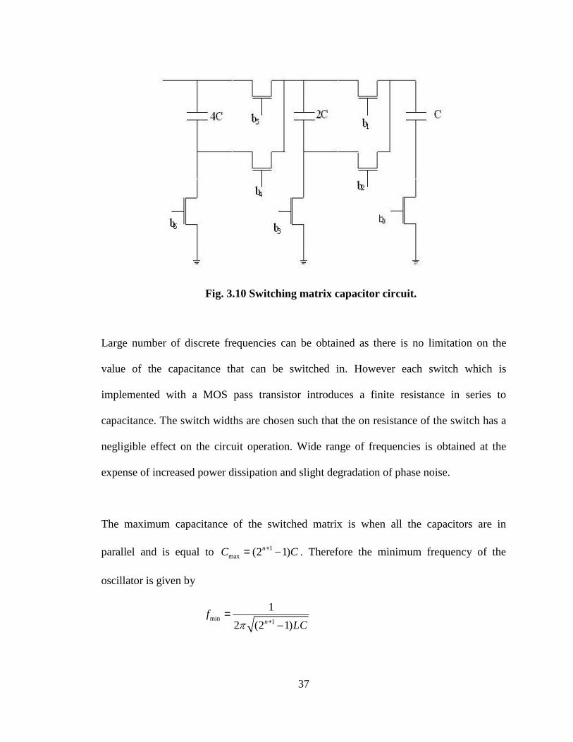
Fig. 3.10 Switching matrix capacitor circuit.
Large number of discrete frequencies can be obtained as there is no limitation on the
value of the capacitance that can be switched in. However each switch which is
implemented with a MOS pass transistor introduces a finite resistance in series to
capacitance. The switch widths are chosen such that the on resistance of the switch has a
negligible effect on the circuit operation. Wide range of frequencies is obtained at the
expense of increased power dissipation and slight degradation of phase noise.
The maximum capacitance of the switched matrix is when all the capacitors are in
parallel and is equal to 1max (2 1)nC C+= − . Therefore the minimum frequency of the
oscillator is given by
min 1
1
2 (2 1)nf
LCπ += −
38
On the other hand, the minimum capacitance is obtained when all the capacitors are
connected in series and is equal to 1
min
2
2 1
n
nC C
−= − and the maximum frequency is given
by max 1
1
22
2 1
n
n
f
LCπ−=
−.

39
40
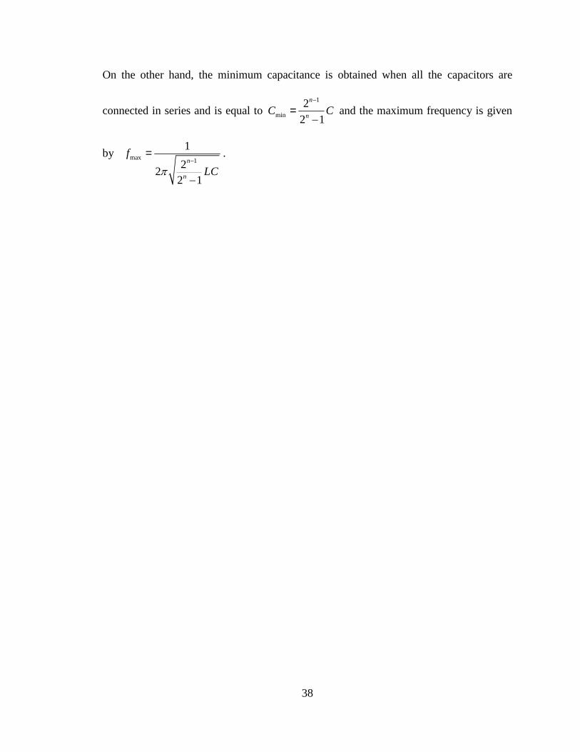
3.4. Results of Reconfigurable Oscillator
For the oscillator circuit a wide tuning range of 25% around the centre frequency is
obtained. Using a switching matrix capacitor circuit consisting of four capacitors, when
all the capacitors are connected in parallel the frequency is observed to be 1.44GHz. On
the other hand, when all the capacitors are connected in series the VCO oscillates at
1.8GHz. The phase noise at 600 KHz offset is observed to be 106dBc/Hz. For different
combinations of capacitors, the phase noise remains basically the same.
Fig. 3.11 Transient Response of Oscillator for the worst case conditionwhen all the switches are ON.
Fig. 3.12 Phase noise of the oscillator circuit for the worst case condition.
41
CHAPTER-4
RECONFIGURABLE CLASS E POWER AMPLIFIER
The power amplifier is a challenging block in the design of a wireless communication
transceiver due to the tradeoffs between supply voltage, output power, power efficiency
and distortion. Instead of limiting efficiency to 50% by maximizing power transfer to the
output, one generally designs a PA to deliver a specified amount of power into the load
with the highest possible efficiency consistent with acceptable power gain and linearity.
4.1 Ideal Class E power Amplifier
An ideal class E power amplifier is shown in Fig. 4.1, which consists of a single power
supply DDV , an RF choke inductor dcL , a switch with a parallel capacitor pC , a resonant
circuit o oL C− and a load LR . The switch is implemented as a MOSFET, which is turned
ON and OFF periodically. The resonant circuit resonates at the input frequency and
passes a sinusoidal current to the load RL, C1 ensures that at the time the switch is turned
off the voltage across the switch still stays relatively low until

42
after the drain current is reduced to zero. The transistor is designed with a large gate
width to reduce the on-resistance so that the switch acts as an ideal switch.
Fig. 4.1 Ideal Class E power amplifier Circuit
4.2 Principles for High Efficiency:
Efficiency is maximized by minimizing the power dissipation, while providing a desired
output power. Maximum power can be obtained if the duty cycle ratio of the input
frequency is made approximately 50 percent [9]. The power dissipation occurs mostly in
the RF power transistor and is given by the product of transistor voltage and current at
each point in time during the RF period, integrated and averaged over RF period. The
product of transistor voltage and current can be made smaller by arranging the circuit
such that the high voltage and high current of the transistor do not exist at the same time.
43
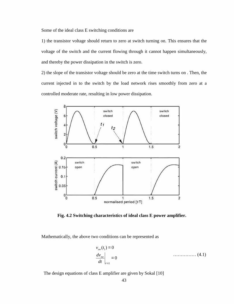
Some of the ideal class E switching conditions are
1) the transistor voltage should return to zero at switch turning on. This ensures that the
voltage of the switch and the current flowing through it cannot happen simultaneously,
and thereby the power dissipation in the switch is zero.
2) the slope of the transistor voltage should be zero at the time switch turns on . Then, the
current injected in to the switch by the load network rises smoothly from zero at a
controlled moderate rate, resulting in low power dissipation.
Fig. 4.2 Switching characteristics of ideal class E power amplifier.
Mathematically, the above two conditions can be represented as
1
1
( ) 0
0
sw
sw
t t
v t
dv
dt =
=
= …………… (4.1)
The design equations of class E amplifier are given by Sokal [10]
44
QRL ω= …………… (4.2)
1
1
5.447C
Rω≈ …………… (4.3)
2 1
5.447 1.421
2.08C C
Q Q
= + −
…………… (4.4)
The maximum power delivered to the load is
2
2
2
1 / 4DD
o
VP
Rπ=+
…………… (4.5)
while the peak drain current is roughly1.7 DDV
R.
Generally the optimum load for the power amplifier is not equal to RF standard load [11].
Therefore it is a common approach that matching networks are employed in RF power
amplifiers.
45
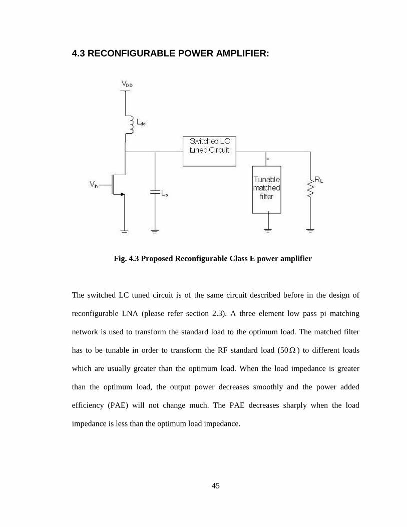
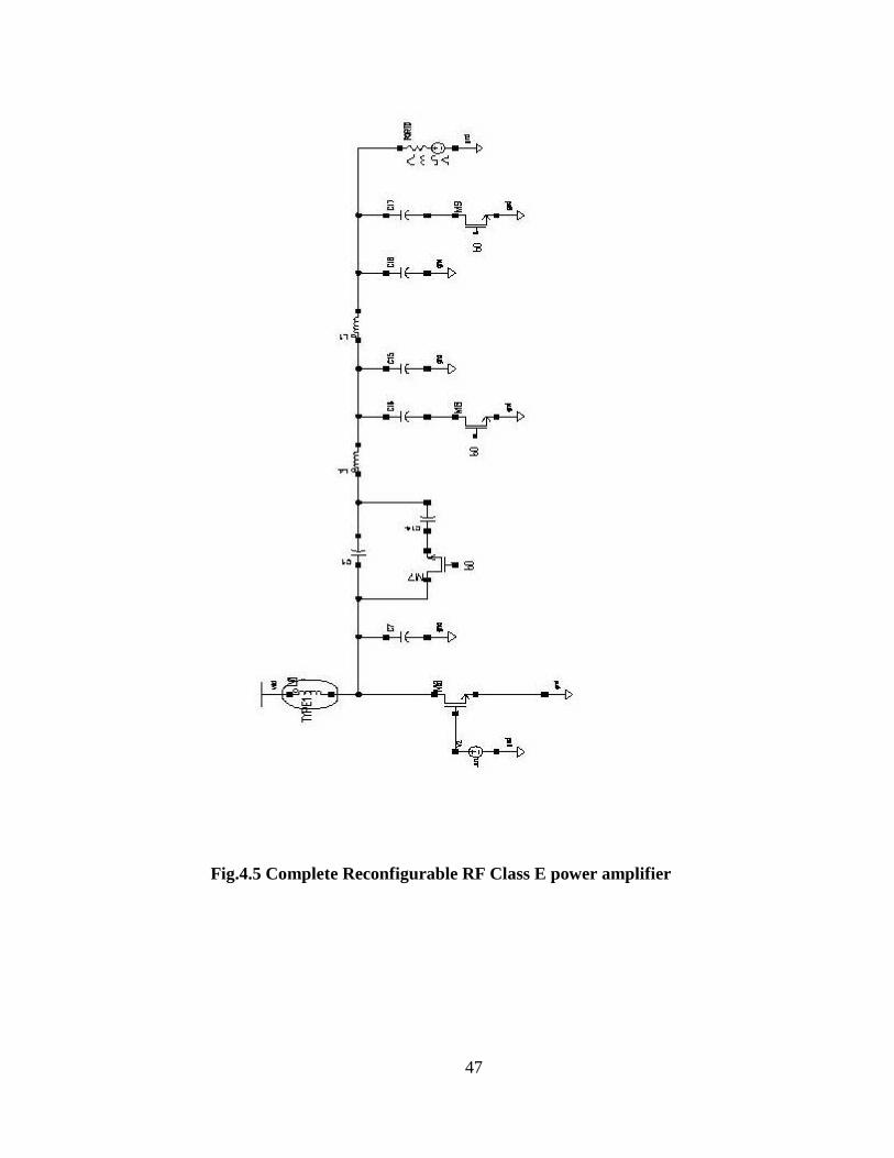
4.3 RECONFIGURABLE POWER AMPLIFIER:
Fig. 4.3 Proposed Reconfigurable Class E power amplifier
The switched LC tuned circuit is of the same circuit described before in the design of
reconfigurable LNA (please refer section 2.3). A three element low pass pi matching
network is used to transform the standard load to the optimum load. The matched filter
has to be tunable in order to transform the RF standard load (50Ω ) to different loads
which are usually greater than the optimum load. When the load impedance is greater
than the optimum load, the output power decreases smoothly and the power added
efficiency (PAE) will not change much. The PAE decreases sharply when the load
impedance is less than the optimum load impedance.
46
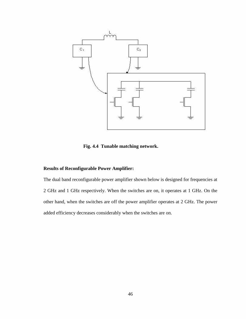
Fig. 4.4 Tunable matching network.
Results of Reconfigurable Power Amplifier:
The dual band reconfigurable power amplifier shown below is designed for frequencies at
2 GHz and 1 GHz respectively. When the switches are on, it operates at 1 GHz. On the
other hand, when the switches are off the power amplifier operates at 2 GHz. The power
added efficiency decreases considerably when the switches are on.
47
Fig.4.5 Complete Reconfigurable RF Class E power amplifier
48
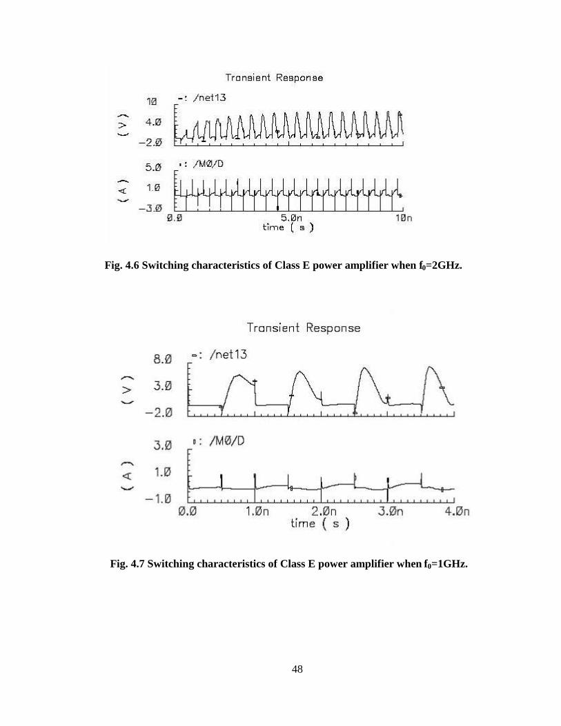
Fig. 4.6 Switching characteristics of Class E power amplifier when f0=2GHz.
Fig. 4.7 Switching characteristics of Class E power amplifier when f0=1GHz.
49
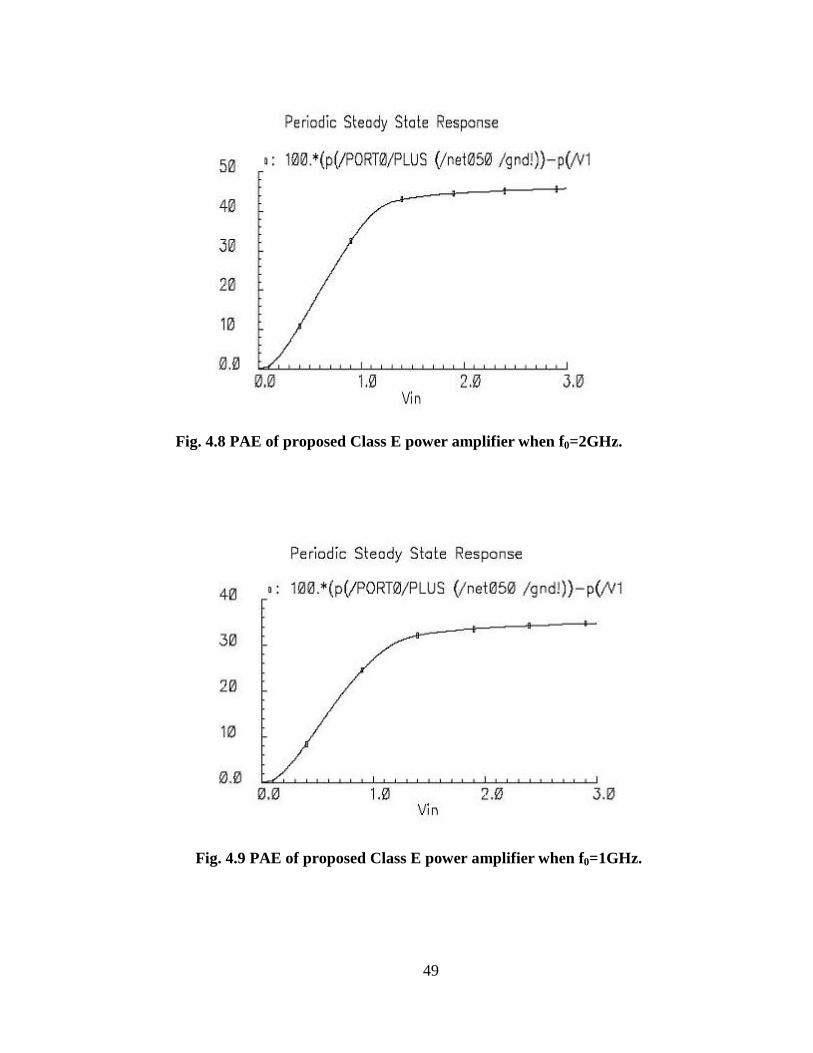
Fig. 4.8 PAE of proposed Class E power amplifier when f0=2GHz.
Fig. 4.9 PAE of proposed Class E power amplifier when f0=1GHz.
50
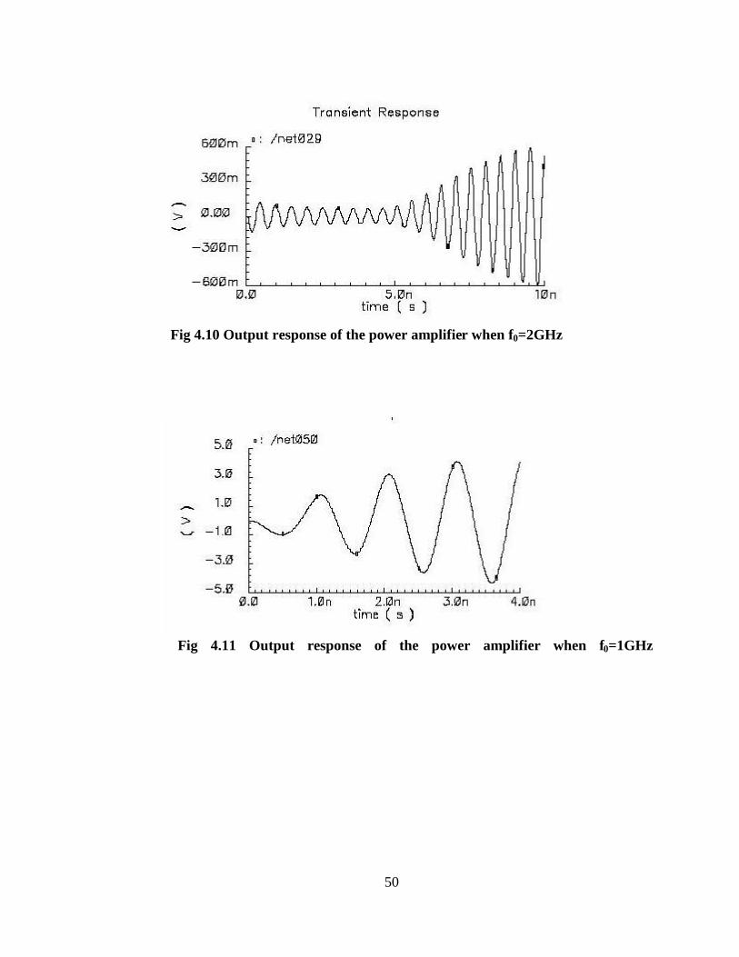
Fig 4.10 Output response of the power amplifier when f0=2GHz
Fig 4.11 Output response of the power amplifier when f0=1GHz
51
CHAPTER- 5
RECONFIGURABLE FILTER
The reconfigurable filter presented in this report consists of a bank of inductors and
capacitors. The reconfiguration here is again done by a switching network. Depending on
the digital control inputs to the switching network, the filter can be reconfigured to one of
the four types of filters namely low-pass, high-pass, band-pass and band-stop filters. Fig
3.1 shows the circuit diagram of the filter.
Because each MOS switch contributes to the attenuation of the input signal due to its
finite on resistance, the switch width must be chosen accordingly to reduce the penalty.
On the other hand, the transistors cannot be made arbitrarily wide either, as the parasitic
capacitances can change the operation of the circuit.

52
Fig. 5.1 Reconfigurable Filter
Table 5.1 Table showing the digital control inputs to the filter.
Type of filter Digital word b3b2b1b0
Low pass 0100 High pass 0001 Band pass 0010 Band stop 1011
53
5.1 Results of Reconfigurable Filter
In the case of Reconfigurable filter, the low-pass filter implemented by setting the control
input to 0100, while the high pass filter implemented by setting the control input to 0001
has the 3dB cutoff frequencies between 0.5GHz and 2.5GHz. The band pass and band
stop filters obtained by setting the respective digital control words as 0010 and 1011
respectively.
Fig. 5.2 Low pass frequency response of the filter
Fig 5.3 band pass frequency response of the filter
54
Fig. 5.4 High pass frequency response of the filter
Fig. 5.5 Band stop frequency response of the filter

55
CHAPTER-6
CONCLUSIONS AND SCOPE FOR FUTURE WORK
6.1 Conclusion
The main objective of this thesis is to design RF circuits which can be
reconfigurable. The advantage of doing this is that the same hardware can be used for
different frequencies. The reconfiguration of the Radio frequency circuits for different
frequencies comes at the expense of a slight degradation of performance metrics of the
circuits. This slight degradation can be tolerated when compared to the advantage of
reusing the same hardware platform. The higher the order of reconfigurability, the higher
the resulting noise figure of the low noise amplifier. Also, the switched matrix circuit
used for tuning the oscillator greatly enhances the flexibility of the oscillator without
much degradation of the phase noise. The power added efficiency decreases from 46% to
35% when the power amplifier is reconfigured.
6.2 Future work
The performance metrics for the different RF circuits described in this thesis can be
optimized. For example, the noise figure of the low noise amplifier can be made to
degrade less by considering the parasitic capacitances of the switched capacitor array.
56
Similarly, phase noise of the oscillator can be optimized by properly sizing the NMOS
and PMOS transistors of the cross coupled LC oscillators. The power added efficiency of
the power amplifier can be increased further by properly designing the output matching
network. The order of the filter can be increased by including more number of resonant
circuits.

57
REFERENCES
[1] Thomas H. Lee, The Design of CMOS Radio-Frequency Integrated Circuits,
Cambridge University press, 1998.
[2] A. Van der Ziel, “Noise in solid state devices and lasers,” Proc. IEEE, vol 58,
pp. 1178-1206, August 1970.
[3] Michael Perrott, EECS 6.976 Course notes, MIT, 2003.
[4] Behzad Razavi, Design of Analog CMOS Integrated circuits, Tata McGraw-Hill, New
York, 2003.
[5] Nathan Sneed, “A 2-GHz CMOS LC tuned VCO using switched-capacitors to
compensate for bond wire Inductance variation”, MS thesis, University of California,
Berkeley.
[6] Ali Hajimiri and Thomas Lee, “Design issues in CMOS differential LC oscillators”,
IEEE J. Solid State Circuits, vol. 34, pp. 717-724, May 1999.
[7] Behzad Razavi, “A study of phase noise in CMOS oscillators”, IEEE J .Solid State
Circuits, Vol. 31, pp. 331-343, March 1996.
[8] Thomas Lee and Ali Hajimiri, “Oscillator phase noise-a tutorial”, IEEE J. Solid State
Circuits, Vol. 35, pp. 326-336, March 2000.
[9] F. H. Raab, “Idealized operation of the class E tuned power amplifier,” IEEE trans.
Circuits and Systems, Vol. 24, pp. 725-735, December 1977.

58
[10] N. O. Sokal and A. D. Sokal, “Class E, a new class of high efficiency tuned single
ended power amplifiers,” IEEE J. Solid State Circuits, vol.10, pp. 168-176, June 1975.
[11] T.Sowlati, “Low Voltage, High efficiency GaAs Class E power amplifier for
wireless Transmitters,” IEEE J. Solid State Circuits, vol. 30, pp. 1074-80,
VITA
Deepak Domalapally
Candidate for the degree of
Master of Science
Thesis: Reconfigurable Radio Frequency Circuits.
Major Field: Electrical and Computer Engineering.
Biographical:
Personal Data: Born in Hyderabad, Andhra Pradesh, India, on Nov19 1979.
Education: Graduated from Little Flower Junior College, Hyderabad, India. Received Bachelor of Technology degree in Electronics and Communications Engineering from Jawaharlal Nehru Technology University, Hyderabad, India in June 1998.Completed the requirements for the Master of Science degree with a major in Electrical and Computer Engineering at Oklahoma State University, Stillwater, Oklahoma in May 2005.
Experience: Employed by Oklahoma State University, Department of Electrical and Computer Engineering as a graduate teaching assistant from August 2004 to present.
Professional Memberships: Student Member of IEEE.
Name: Deepak Domalapally Date of Degree: May 2005
Institution: Oklahoma State University Location: Stillwater, Oklahoma
Title of Study: RECONFIGURABLE RADIO FREQUENCY CIRCUITS
Pages in Study: 58 Candidate for the Degree of Master of Science
Major Field: Electrical and Computer Engineering.
Scope and Method of Study: The diverse range of wireless applications necessitates communication systems with more bandwidth and flexibility. It is necessary to design a flexible radio frequency front end for handling a wide range of carrier frequencies. Therefore, an effort has been made in this thesis to increase the flexibility of RF front end circuits like LNA, Oscillator, Power amplifier and filter.
Findings and Conclusions: The advantage in reconfiguring the RF circuits is that the same hardware platform can be used for different frequencies. The reconfigurable filter greatly reduces the size of the circuit by suing the same set of inductors and capacitors. Also, the switched matrix circuit used for tuning the oscillator enhances the flexibility of the oscillator without much degradation of phase noise. The higher the order of reconfigurability, the higher the noise figure of the low noise amplifier. For the power amplifier, the power added efficiency decreases slightly when it is reconfigured.
ADVISER’S APPROVAL: Dr.Yumin Zhang