Embed Size (px)
Citation preview

Reconfigurable Logic
for Low-Power Space Systems
by
Jeffrey D. Poznanovic
A thesis submitted to the
Faculty of the
University of Colorado in partial fulfillment
of the requirements for the degree of
Bachelor of Science
Department of Computer Science
2004
This thesis entitled:Reconfigurable Logic
for Low-Power Space Systemswritten by Jeffrey D. Poznanovic
has been approved for the Department of Computer Science
Dirk Grunwald
Prof. Dan Connors
Prof. Rick Han
Date
The final copy of this thesis has been examined by the signatories, and we findthat both the content and the form meet acceptable presentation standards of
scholarly work in the above mentioned discipline.
iii
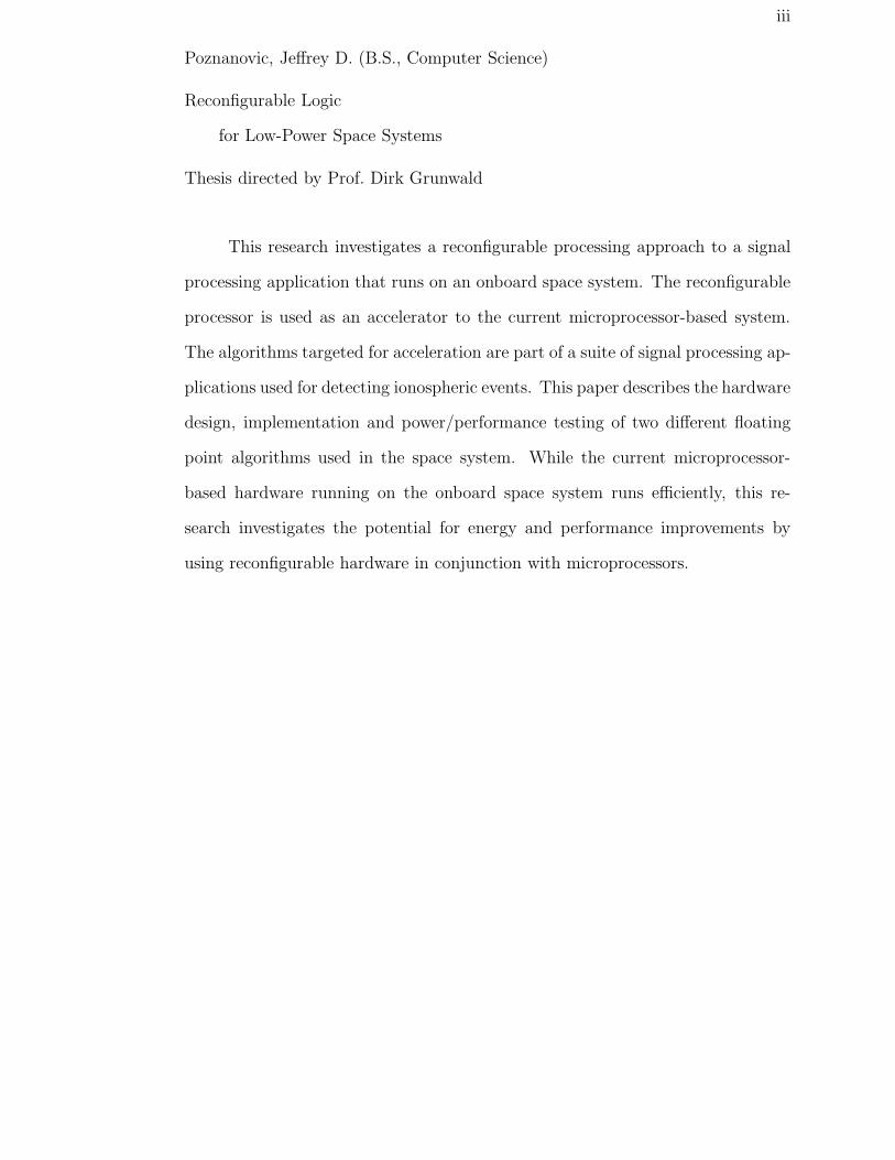
Poznanovic, Jeffrey D. (B.S., Computer Science)
Reconfigurable Logic
for Low-Power Space Systems
Thesis directed by Prof. Dirk Grunwald
This research investigates a reconfigurable processing approach to a signal
processing application that runs on an onboard space system. The reconfigurable
processor is used as an accelerator to the current microprocessor-based system.
The algorithms targeted for acceleration are part of a suite of signal processing ap-
plications used for detecting ionospheric events. This paper describes the hardware
design, implementation and power/performance testing of two different floating
point algorithms used in the space system. While the current microprocessor-
based hardware running on the onboard space system runs efficiently, this re-
search investigates the potential for energy and performance improvements by
using reconfigurable hardware in conjunction with microprocessors.

Dedication
This work is dedicated to my parents, Linda and Dan, whose support and
kindness was deeply appreciated.

v
Acknowledgements
Thanks to my mentors, Jan Frigo, Maya Gokhale and Patrick Shriver, at
the Los Alamos National Laboratory for their guidance and to Nathan Rollins for
his assistance with XPower.
vi
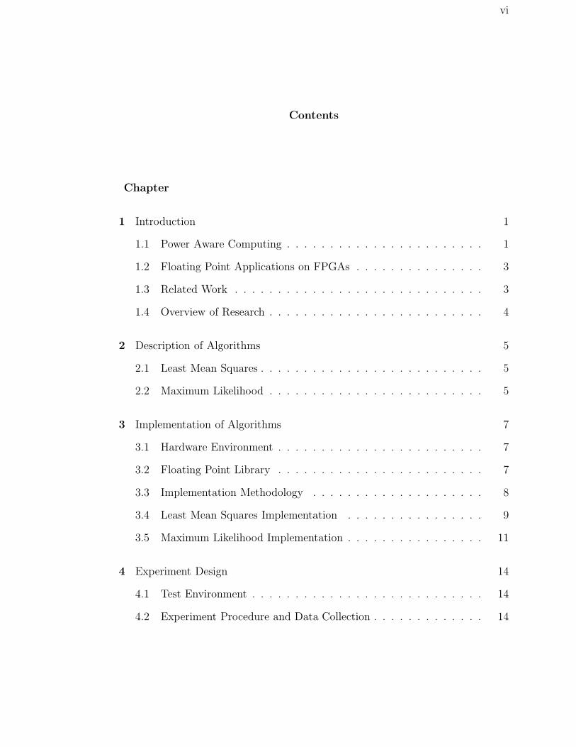
Contents
Chapter
1 Introduction 1
1.1 Power Aware Computing . . . . . . . . . . . . . . . . . . . . . . . 1
1.2 Floating Point Applications on FPGAs . . . . . . . . . . . . . . . 3
1.3 Related Work . . . . . . . . . . . . . . . . . . . . . . . . . . . . . 3
1.4 Overview of Research . . . . . . . . . . . . . . . . . . . . . . . . . 4
2 Description of Algorithms 5
2.1 Least Mean Squares . . . . . . . . . . . . . . . . . . . . . . . . . . 5
2.2 Maximum Likelihood . . . . . . . . . . . . . . . . . . . . . . . . . 5
3 Implementation of Algorithms 7
3.1 Hardware Environment . . . . . . . . . . . . . . . . . . . . . . . . 7
3.2 Floating Point Library . . . . . . . . . . . . . . . . . . . . . . . . 7
3.3 Implementation Methodology . . . . . . . . . . . . . . . . . . . . 8
3.4 Least Mean Squares Implementation . . . . . . . . . . . . . . . . 9
3.5 Maximum Likelihood Implementation . . . . . . . . . . . . . . . . 11
4 Experiment Design 14
4.1 Test Environment . . . . . . . . . . . . . . . . . . . . . . . . . . . 14
4.2 Experiment Procedure and Data Collection . . . . . . . . . . . . . 14

vii
5 Experiment Results 16
5.1 Method of Analysis . . . . . . . . . . . . . . . . . . . . . . . . . . 16
5.2 Analysis of Results . . . . . . . . . . . . . . . . . . . . . . . . . . 19
5.2.1 Least Mean Squares Analysis . . . . . . . . . . . . . . . . 19
5.2.2 Maximum Likelihood Analysis . . . . . . . . . . . . . . . . 23
6 Conclusions 28
Bibliography 30
viii
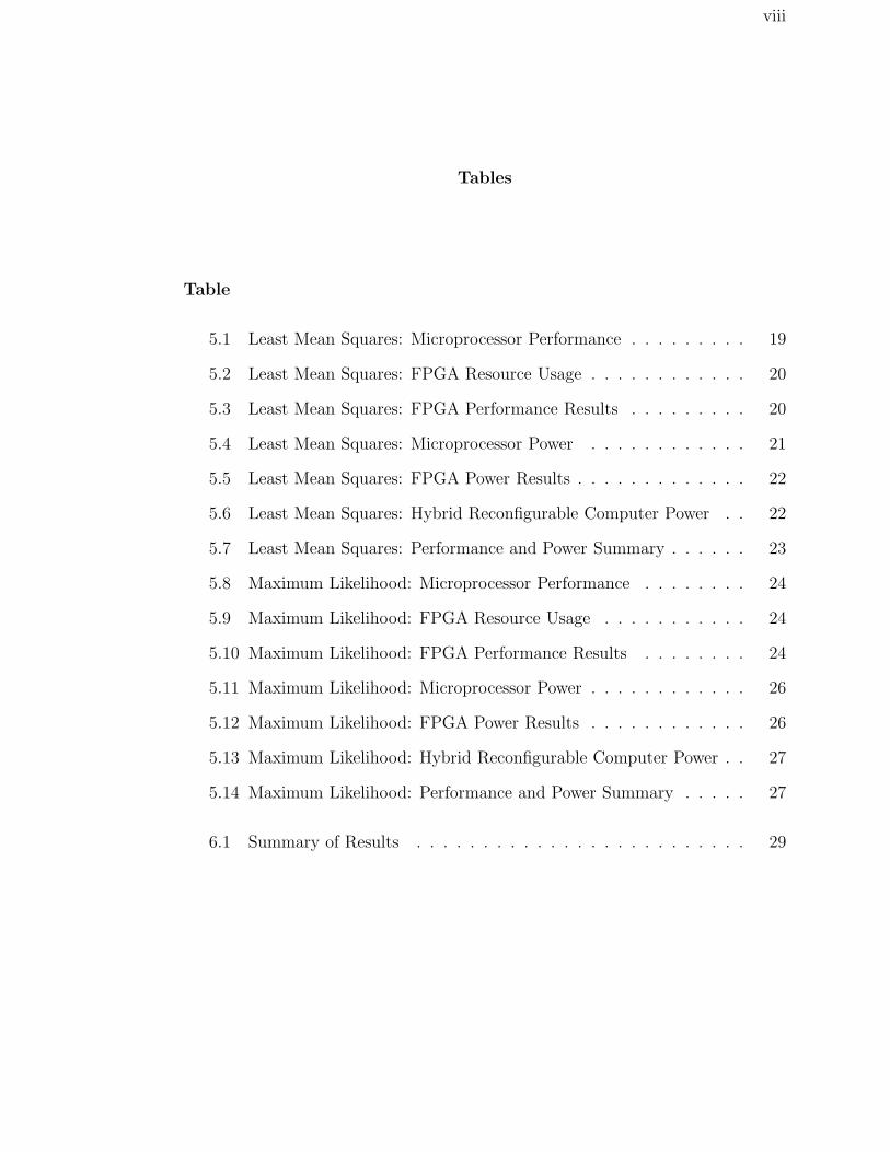
Tables
Table
5.1 Least Mean Squares: Microprocessor Performance . . . . . . . . . 19
5.2 Least Mean Squares: FPGA Resource Usage . . . . . . . . . . . . 20
5.3 Least Mean Squares: FPGA Performance Results . . . . . . . . . 20
5.4 Least Mean Squares: Microprocessor Power . . . . . . . . . . . . 21
5.5 Least Mean Squares: FPGA Power Results . . . . . . . . . . . . . 22
5.6 Least Mean Squares: Hybrid Reconfigurable Computer Power . . 22
5.7 Least Mean Squares: Performance and Power Summary . . . . . . 23
5.8 Maximum Likelihood: Microprocessor Performance . . . . . . . . 24
5.9 Maximum Likelihood: FPGA Resource Usage . . . . . . . . . . . 24
5.10 Maximum Likelihood: FPGA Performance Results . . . . . . . . 24
5.11 Maximum Likelihood: Microprocessor Power . . . . . . . . . . . . 26
5.12 Maximum Likelihood: FPGA Power Results . . . . . . . . . . . . 26
5.13 Maximum Likelihood: Hybrid Reconfigurable Computer Power . . 27
5.14 Maximum Likelihood: Performance and Power Summary . . . . . 27
6.1 Summary of Results . . . . . . . . . . . . . . . . . . . . . . . . . 29

ix
Figures
Figure
3.1 Eight-input pipelined adder tree . . . . . . . . . . . . . . . . . . . 10
3.2 Least mean squares pipelined hardware design . . . . . . . . . . . 10
3.3 Eight-input pipelined median solver . . . . . . . . . . . . . . . . . 13
3.4 Maximum likelihood pipelined hardware design . . . . . . . . . . 13
Chapter 1
Introduction
1.1 Power Aware Computing
Power-Aware Computing (PAC) technology was developed at the Los Alamos
National Laboratory (LANL) to aid in the detection of transient radio frequency
events (e.g., lightning) as observed from the FORTE satellite. There’s been a
shift towards onboard processing of data as opposed to ground-based processing.
The main reasons for this shift towards onboard processing are as follows: mod-
ern instrument technology requires increased power for transmissions, onboard
processing can reduce bandwidth requirements via data reduction, data latency
increases the duration before processed data reaches the end user, and onboard
analysis can improve the detection capability of the system.
The PAC system utilizes four different signal processing algorithms for the
detection of ionospheric events. These floating-point algorithms include a Least-
Mean-Squares (LMS), Maximum Likelihood (ML), Software Trigger (ST), and a
bank of Matched Filters (MF). Each algorithm varies based on accuracy, execution
time, and power expenditure. The power consumption 1 differences between the
four algorithms is a 106 order of magnitude [15]. In this case, the more accurate
an algorithm is at detecting ionospheric events, the more energy it consumes. The
1 In our terminology for this paper, ”power consumption” implies a time duration over which
the power is consumed, not an instantaneous measure, e.g. Watts. Power consumed over time
is expressed as energy, e.g. Joules.

2
PAC system determines which algorithm to use based on the currently available
energy of the onboard computer.
The current PAC system targets the Power Aware Multiprocessor Architec-
ture (PAMA) hardware to demonstrate and evaluate the Algorithm Power Modu-
lation (APM) technology. PAMA is a 4-node, multiprocessor board under devel-
opment by the Information Sciences Institute. Each Hitachi SH-4 processor, with
32-bit integer and floating point hardware, on the PAMA-2 board is connected by
a programmable interconnect. The system software includes the Linux operating
system, MPI-like communications between processes, and a power-aware software
library that allows applications to query power levels and set processor mode,
clock frequency, and voltage [16].
The application is partitioned between the four processors in the following
way. One node is designated as the application controller, and the three remaining
are designated as worker nodes. The controller node sends control vectors to the
worker nodes telling them which filter to apply to which incoming data set. In a
low-power, high-event-rate situation, the workers each perform least means square
fit or the maximum likelihood fit on separate, unique data streams. This allows for
quick event detection. In a high-power, low-event-rate scenario, each worker gets
the same data but different filters. In this scenario, when another event occurs,
the controller takes the most accurate result computed and resets the workers to
a new event [16].
While the current hardware of the PAC system runs efficiently, this research
investigates the potential for energy and performance improvements by using re-
configurable hardware in conjunction with microprocessors. This research focuses
on two of the four signal processing algorithms (least mean squares and maxi-
mum likelihood) due to the range of complexities associated with mapping each
algorithm to hardware.
3
1.2 Floating Point Applications on FPGAs
Over the past decade, FPGAs have been consistently seen as a very capa-
ble alternative to microprocessors—as long as the computation involves no float-
ing point arithmetic. Recently, the large increase in logic density and the addi-
tion of embedded arithmetic units has enabled efficient, high-performance floating
point computation on FPGAs. Research into application-specific floating point
pipelines have shown to produce order of magnitude performance increases over
microprocessor implementations [5]. The future of FPGA performance appears
quite promising. While CPUs follow the well known corollary of Moore’s Law
(doubling in performance every 18 months), FPGA performance increases by four
times every two years [17].
Both the least mean squares and maximum likelihood algorithms are based
on floating point computations.
1.3 Related Work
Over the past few years there has been much research into implementing
floating point algorithms on FPGAs. Early work [11] found that FPGAs were
not fast enough to compete with microprocessor-based floating point computation.
More recently, with improved FPGA technology, research has shown more promis-
ing results for FPGA-based floating point computation. Sahin et. al. found that
highly-pipelined floating point accumulators ran 9 to 14 times faster than soft-
ware implementations [14]. Belanovic and Leeser [1] presented a parameterized
floating-point library and its use in a K-means clustering application. Wang [18]
extended Belanovic and Leeser’s library to include floating point division and
square root operators, which allowed for a faster implementation of the K-means
clustering application.
4
There has also been a lot of work on the power/energy consumption of
FPGA-based computing systems. When computing matrix multiply operations,
Prasanna and others found that FPGA based floating point architectures can
achieve 6× improvements in terms of performance per unit power over that of mi-
croprocessors [7]. The University of Massachusetts has been researching power-
aware video applications for FPGAs [2]. Energy-efficient FFT and matrix mul-
tiplication designs have been implemented on FPGAs and shown to outperform
DSPs in energy consumption [3].
1.4 Overview of Research
As stated previously, reconfigurable computing has recently demonstrated
huge power and performance gains on data- and compute-intensive applications
involving floating point computation. This paper describes the hardware design,
implementation and power/performance testing of two different floating point al-
gorithms. The algorithms are part of a suite of signal processing applications
used for detecting ionospheric events. This research investigates the potential for
energy and performance improvements by using reconfigurable hardware in con-
junction with microprocessors. The power and performance results are compared
to the current microprocessor-based implementation.
Chapter 2
Description of Algorithms
2.1 Least Mean Squares
The least mean squares algorithm solves the problem of fitting a set of N
data points (xi, yi) to a straight-line model
y(x) = y(x; a, b) = a + bx
This problem is often called linear regression. An assumption must be made that
the uncertainty σi associated with each yi is known and that the xi’s are known
exactly.
The LMS algorithm [12]:
ti = 1
σi(xi −
Sx
S), i = 1, 2, ..., N
Stt =N∑
i=1
t2i
b = 1
Stt
N∑
i=1
tiyi
σi
a = Sy−Sxb
S
2.2 Maximum Likelihood
The Maximum Likelihood algorithm is a robust statistical method. Robust
methods are desirable when statistical fluctuations due to outliers prevent accu-
rate fitting of a straight line to a two-dimensional distribution. So in a sense, it
performs the same function as the least mean squares, although it is resistant to

6
outliers which skew the fit of the line.
The algorithm initially performs a least mean squares fit on the points to
gain an estimate of the fit of the straight line. Based on the estimate, it then finds
a root via the bisection method. To set up the initial brackets for the bisection
method, a function is used to find the median of the distribution. This function is
also used in the bisection method to determine which half of the current interval
to use as the next interval.
Here is the part of the ML algorithm that helps set up for the bisection root
finding method [12]:
a = median{yi − bxi}
0 =N∑
i=1
xi sgn(yi − a − bxi)
Chapter 3
Implementation of Algorithms
3.1 Hardware Environment
For the mapping of the suite of signal processing algorithms to hardware,
the Xilinx Virtex II and Virtex II Pro were targeted. These devices have small
embedded memories called block RAMs in addition to 18-bit multipliers, which
enable efficient floating point performance.
3.2 Floating Point Library
Various commercial [9, 10] and open source [1, 13] floating point libraries
are available. For the implementation of least mean squares and maximum likeli-
hood, we chose the FPLibrary, a VHDL library of hardware operators for floating-
point computation, developed by the Arenaire project [4]. Three requirements de-
termined our decision. First, the library was developed using VHDL in a platform
independent manner, which allows for easy porting to multiple FPGA architec-
tures. Second, the library implements addition, multiply, and divide floating point
operations, which were all required for these applications. Third, the modules and
floating point types have parameterizable bitwidths, which allows flexibility in our
implementation.
8
3.3 Implementation Methodology
When considering which part of the algorithm to implement on the FPGA,
profiling the code seemed to be the most effective method to check where most
of the execution time was spent in the application. Optimally, profiling would
have been conducted on a RAD750 processor (the same processor as the one used
in the PAMA architecture), but without access to such a processor, a somewhat
more standard processor was used. A 1.5 GHz Intel Pentium M processor with
512 MB RAM was used instead of the radiation hardened processor.
A fully pipelined design was the goal of transformation from C source code
to a hardware implementation. Reconfigurable computing can often easily exploit
the spatial parallelism of an algorithm by duplicating functional units that were
sequentially computed in a von Neumann type implementation—but, this isn’t
where reconfigurable computing really gains its performance. Data pipelining is
another form of parallelism that can have immense effect on the performance
of a reconfigurable computing application—in many cases, this can be the most
influential in performance which allows reconfigurable computing to overcome its
relatively slower clock speeds. Data pipelining allows an input to be fed to the
hardware design once per clock cycle. For example, if the number of inputs to the
hardware design far outweighs the latency of the pipeline, the average number of
outputs per clock cycle is near one.
After the decision on what part of the algorithms to implement in hardware,
it was important to understand the pipeline involved in what we planned to im-
plement. In order to get an approximation of the pipelines, initial integer-based
VHDL designs for each algorithm were generated using Streams-C [6]. After the
pipelines were fully understood, VHDL designs were manually developed for each
algorithm using the floating point libraries specified in the preceding section.

9
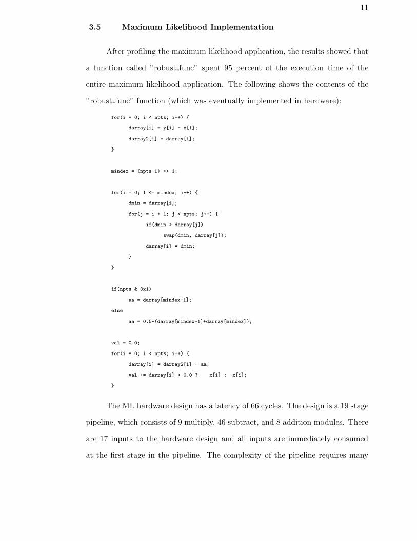
3.4 Least Mean Squares Implementation
Realization of the LMS hardware logic came from examining the C source
code that was developed for the microprocessor-based implementation. Profiling
of the LMS application showed that 83.3 percent of the execution time was spent
in a function called ”linregress.” This function is the section of the source code
that was chosen for hardware optimization:
S = (double) numdatapts;
for (I=0;I<numdatapts;I++)
{
Sx += *(indep_data + I);
Sy += *(dep_data + I);
}
Sx_ovr_S = Sx/S;
for (I=0;I<numdatapts;I++)
{
t=*(indep_data+I)-Sx_ovr_S;
Stt += t*t;
*slope += t * *(dep_data+I);
}
*slope /= Stt;
*y_int = (Sy - Sx*(*slope))/S;
The thirteen stage pipeline of the LMS design has a latency of 77 cycles. The
design consists of 28 addition, 2 subtraction, 3 division, and 3 multiply modules.
There are 20 inputs to the pipeline at each clock, which are consumed at various
points of the pipeline. The complexity of the pipeline requires many intermediate
registers for pipelining purposes—in total, 526 registers. These registers are used
to ”delay” data when the data is being used in a later section of the pipeline.
10
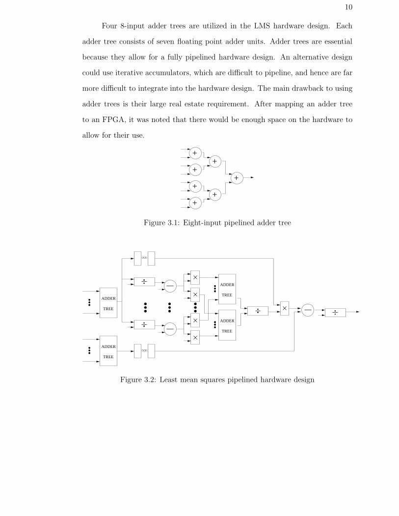
Four 8-input adder trees are utilized in the LMS hardware design. Each
adder tree consists of seven floating point adder units. Adder trees are essential
because they allow for a fully pipelined hardware design. An alternative design
could use iterative accumulators, which are difficult to pipeline, and hence are far
more difficult to integrate into the hardware design. The main drawback to using
adder trees is their large real estate requirement. After mapping an adder tree
to an FPGA, it was noted that there would be enough space on the hardware to
allow for their use.
+
+
+
+
+
+
+
Figure 3.1: Eight-input pipelined adder tree
TREE
ADDER
TREE
ADDER
TREE
ADDER
TREE
ADDER
Figure 3.2: Least mean squares pipelined hardware design
11
3.5 Maximum Likelihood Implementation
After profiling the maximum likelihood application, the results showed that
a function called ”robust func” spent 95 percent of the execution time of the
entire maximum likelihood application. The following shows the contents of the
”robust func” function (which was eventually implemented in hardware):
for(i = 0; i < npts; i++) {
darray[i] = y[i] - x[i];
darray2[i] = darray[i];
}
mindex = (npts+1) >> 1;
for(i = 0; I <= mindex; i++) {
dmin = darray[i];
for(j = i + 1; j < npts; j++) {
if(dmin > darray[j])
swap(dmin, darray[j]);
darray[i] = dmin;
}
}
if(npts & 0x1)
aa = darray[mindex-1];
else
aa = 0.5*(darray[mindex-1]+darray[mindex]);
val = 0.0;
for(i = 0; i < npts; i++) {
darray[i] = darray2[i] - aa;
val += darray[i] > 0.0 ? x[i] : -x[i];
}
The ML hardware design has a latency of 66 cycles. The design is a 19 stage
pipeline, which consists of 9 multiply, 46 subtract, and 8 addition modules. There
are 17 inputs to the hardware design and all inputs are immediately consumed
at the first stage in the pipeline. The complexity of the pipeline requires many
12
intermediate registers for pipelining purposes—in total, 210 registers. Again, these
registers are used to ”delay” data when the data is being used in a later section
of the pipeline.
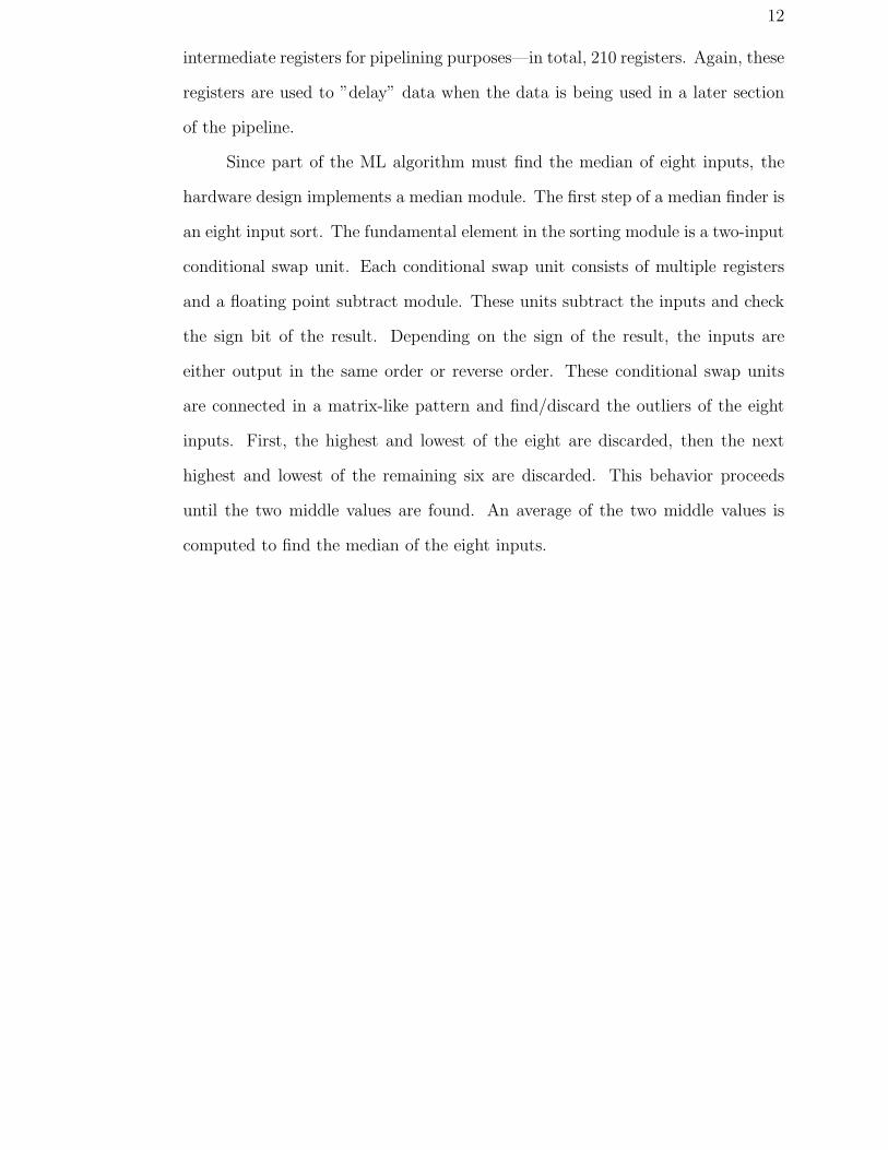
Since part of the ML algorithm must find the median of eight inputs, the
hardware design implements a median module. The first step of a median finder is
an eight input sort. The fundamental element in the sorting module is a two-input
conditional swap unit. Each conditional swap unit consists of multiple registers
and a floating point subtract module. These units subtract the inputs and check
the sign bit of the result. Depending on the sign of the result, the inputs are
either output in the same order or reverse order. These conditional swap units
are connected in a matrix-like pattern and find/discard the outliers of the eight
inputs. First, the highest and lowest of the eight are discarded, then the next
highest and lowest of the remaining six are discarded. This behavior proceeds
until the two middle values are found. An average of the two middle values is
computed to find the median of the eight inputs.
13
+
0.5
Figure 3.3: Eight-input pipelined median solver
fp_median8
sign manip.
sign manip.
sign manip.
sign manip.
sign manip.
sign manip.
sign manip.
sign manip.
fp_adder_tree
Figure 3.4: Maximum likelihood pipelined hardware design
Chapter 4
Experiment Design
4.1 Test Environment
Many programs were used in the process to create and test both of the
hardware designs. Xilinx ISE Foundation 6.3.02 was used for synthesis and place
and route for both of the hardware designs.
XPower was designed by Xilinx to estimate the power consumption of a
given placed FPGA design. Input into XPower can consist of the following types
of design files: *.par.ncd, *.ncd and *.pcf. In addition, XPower takes a VCD file
which is discussed later.
4.2 Experiment Procedure and Data Collection
There were many steps towards obtaining power and performance results
for the two hardware designs–although the steps are the same for both hardware
designs. The first step was to synthesize and place and route the hardware design.
The place and route results gave the percentage of slices, multipliers, I/O buffers
(IOBs), and most importantly, the maximum clock frequency of the design.
The next step was to create a VCD file which was used as an input into
the XPower program. In order for XPower to obtain accurate power consumption
results, each net in the design must have an activity rate assigned to it. If some
signals do not have activity rates assigned, XPower reports a confidence level
15
of ”reasonable,” and if many are not assigned, XPower reports an ”inaccurate”
confidence level [8]. The activity rates are found in the VCD file. The process to
generate the activity rates can be a confusing task. The first step was to generate
a back-annotated VHDL file via the Xilinx tools, which flattens all hierarchy in
the design. XPower supposedly has trouble interpreting design hierarchy. The
next step was to simulate using ModelSim by driving the design with a testbench.
Cryptic commands are input to ModelSim via a ”DO” file. The commands tell
ModelSim to record the activity rates of the signals for a specified amount of time.
After completion of the simulation, ModelSim created a VCD file.
After the design and VCD files were created, XPower was run. XPower
outputs a PWR file that contains the power results of the hardware design.
Chapter 5
Experiment Results
All of the steps in the Experiment Design Section (4.2) are completed and
presented in this chapter.
5.1 Method of Analysis
The analysis of the results focuses on comparing the power and performance
of the hybrid reconfigurable computing implementation to the microprocessor im-
plementation. The least means squares and maximum likelihood algorithms have
separate sections in which to discuss performance and power. First, a section on
the performance results is presented and discussed. This section contains analy-
sis of the microprocessor-based performance, place and route statistics on the
FPGAs, hardware design performance, and total application performance of the
reconfigurable computing system. A section on power analysis follows the perfor-
mance analysis. The power analysis section compares the power results between
the microprocessor and reconfigurable computing implementation.
The microprocessor-based performance results did not include any runs on
larger datasets; the results were obtained from running the application on small
datasets. Therefore, an estimate of the performance had to be made for larger
datasets. The GNU gprof profiler was used to find how much of the application
was spent in the loop overhead and the percentage spent in the section of the code
17
that was implemented in hardware.
The peak performance of an application running on an FPGA occurs when
the hardware design is fully pipelined and the pipeline gets completely filled with
a continuous stream of data. Since the designs are pipelined, the peak number of
FLOPS can be calculated by counting the floating point operations in the design
and dividing by the clock period.
The performance of the application running on the hybrid reconfigurable
computing system is very dependent not only on the hardware designs, but also
on the way the software interacts with the hardware design. To get these designs
to run efficiently on the proposed hybrid reconfigurable system, a few considera-
tions on this hardware-software interaction are extremely important. Since this
computer system isn’t currently available, some scenarios will be discussed in or-
der to estimate the performance of the application. Each scenario will have a
different result in respect to performance and power consumption. The task is
to determine how to setup a correct data pipeline from the side of the software
process.
Complexity arises when loop-carried dependencies exist in the algorithm.
These loop-carried dependencies affect the pipelining of the hardware design be-
cause, in certain circumstances, input to the FPGA is not ready until later iter-
ations of the loop. Therefore, the hardware pipeline would have to stall until the
input is ready. Repeated stalling could significantly affect the performance of the
application.
The worst-case performance scenario occurs when the pipeline cannot be
kept full. In this situation, after inputting to the design, one must wait the
entire latency of the design to be able to input again. Here, spatial parallelism
could still allow for some performance acceleration, but it would be extremely
inefficient compared to an implementation that fully utilizes the pipeline. This
18
situation occurs when the microprocessor loop stalls with each invocation of the
hardware routine. Stalling of the software loop could occur due to loop-carried
dependencies.
The best-case scenario is of course when the hardware design is fully pipelined
and the software loop keeps the pipeline full. Here, the data must be readily avail-
able in each iteration of the loop. During every FPGA cycle, a set of inputs must
be supplied by the software process. All loop-carried dependencies have to be
handled or removed from the loop in order to provide an input every cycle. To
analyze this scenario, the performance of the hardware design has to be integrated
with the performance of the software loop that drives the design. The previous
profiler results are used to find the percentage of time spent outside of the code
that was implemented in hardware.
A streaming producer-consumer model of computation can be utilized in an
attempt to keep the pipeline full. One such compiler with a streaming model is
the Streams-C compiler [6].
Finally, there are a few assumptions I will make about the target recon-
figurable computing system. First, the computing system must have a closely-
coupled CPU and FPGA. Since I’ve made this assumption, there would be neg-
ligible overhead involved with the data transfer between CPU and FPGA in the
reconfigurable computing implementation. An example of a closely-coupled CPU
and FPGA system is the Xilinx Virtex II Pro FPGA, which has integrated Power
PC cores in the FPGA fabric. Also, a long continuous stream of input (which is
common for signal processing applications) should be assumed so that the effect
of pipeline latency diminishes. Many of the results will use 1,000,000 inputs due
to this assumption.
19% of Application Time/Input(sec) Million Input Time(mSec)
Loop Overhead 16.7 2.6 × 10⁻⁸ 27.1Function 83.3 1.349 × 10⁻⁷ 134.9
Table 5.1: Least Mean Squares: Microprocessor Performance
5.2 Analysis of Results
5.2.1 Least Mean Squares Analysis
5.2.1.1 Performance
Microprocessor Performance
The microprocessor-based performance results did not include any runs on
larger datasets; the results were obtained from running the application on 21
data points. Therefore, an estimate of the performance had to be made. From
earlier gprof profiling of the LMS application, 83.3% of the time spent in the
application was in the portion of code that was implemented in hardware and
16.7% was in the loop overhead. The execution time of the LMS algorithm plus
the overhead for controlling the loop for 21 data points was 3.4 × 10⁻⁶ seconds.
After reducing the execution time by 16.7% to account for the loop overhead, it
takes 2.832×10⁻⁶ seconds to run 21 inputs. Then divide by 21 to get the average
execution time per data point — 1.349 × 10⁻⁷ seconds. For 10,000 inputs, the
execution time would take 1.3 milliseconds. For 100,000 inputs, it would take 13.4
milliseconds. Since there’s a linear relation here, just shift the decimal point again
to get 134.9 milliseconds for 1,000,000 inputs. For both the LMS algorithm and
the loop overhead, performance would be 1.62 milliseconds for 10,000 inputs, 16.2
milliseconds for 100,000 inputs, and 162 milliseconds for 1,000,000 inputs.
FPGA LMS Resource Usage The statistics for the FPGA resource
usage are shown in Table 5.2. The results for the xc2v6000 were omitted because
20V2-6000 V2P-70 V2P-100
% Slices * 59 44% Multipliers * 62 45
% External IOBs * 61 58
Table 5.2: Least Mean Squares: FPGA Resource Usage
an error consistently occurred during the place and route stage.
FPGA LMS Performance
For the FPGA design, 77 cycles of latency (minus one) are added to the
number of inputs to the pipeline to get the total number of cycles needed for com-
putation. So 10,000 inputs would give a cycle count of 10,076. One-hundred thou-
sand inputs would give 100,076 cycles, and 1,000,000 inputs would give 1,000,076
cycles. Therefore, to compute 1,000,000 inputs at a rate of 57.1 MHz (on the
xc2vp100 FPGA), it would take 17.5 milliseconds. This is an improvement of
7.7 times between the FPGA and microprocessor implementations (excluding the
loop overhead). Thirty-six floating point units are included in the LMS hardware
design. Therefore, with a clock speed of 57.1 MHz (on the xc2vp100 FPGA), the
LMS design is capable of delivering 2.06 GFLOPS.
V2-6000 V2P-70 V2P-100
Freq. (MHz) * 45.87 57.14Latency (cycles) * 77 77
GFLOPS * 1.7 2.06Time/input(ns) * 21.8 17.5
Million Input Time(mSec) * 21.8 17.5
Table 5.3: Least Mean Squares: FPGA Performance Results
Hybrid Reconfigurable Computer LMS Performance
When finding the total application performance on the reconfigurable com-
puter, it’s important to consider the software that drives the hardware design.
The loop driving the inputs to the LMS hardware design is very straightforward.
21% of Application Energy/Input(J) Million Input Energy(mJ)
Loop Overhead 16.7 1.48 × 10⁻⁷ 148.71Function 83.3 7.41 × 10⁻⁷ 741.76
Table 5.4: Least Mean Squares: Microprocessor Power
No loop-carried dependencies exist, which allows for a completely filled pipeline.
Therefore, to find the total application performance for the reconfigurable com-
puter, add the loop overhead of the microprocessor to the FPGA performance.
The result is 44.6 milliseconds to compute 1,000,000 inputs.
Calculations for the Hybrid Performance --
Microprocessor loop overhead: X = 27.1 milliseconds (16.7\% of 162 milliseconds)
Hardware design latency: L = 77 cycles
xc2vp100 FPGA clk period: p = 17.5 ns
Time to compute 1,000,000 inputs: T = X + p * (1000000 + L - 1) = 44.6 milliseconds
5.2.1.2 Power
Microprocessor LMS Power
Once again, due to the lack of RAD750 power testing on the LMS appli-
cation’s large datasets, an estimation had to be made. The microprocessor took
18.7×10⁻⁶ Joules to run the 21 input testbench. To account for the loop overhead,
the energy was reduced by 16.7%. Divide by 21 to get the average energy usage
per unit input — 7.41 × 10⁻⁷ Joules. So, for 10,000 inputs, it would take 7.41
mJ. For 100,000 inputs, the energy consumed would be 74.17 mJ. For 1,000,000
inputs, the microprocessor would take 741.76 mJ. For both the LMS algorithm
and the loop overhead, it would take 890 mJ to compute 1,000,000 inputs.
FPGA LMS Power
The FPGA power results came from the XPower power estimation appli-
cation as discussed in the previous chapter. With a rate of 6.074 × 10⁻⁸ Joules
per cycle for the xc2vp100, one-million and seventy-six cycles (from 1,000,000 in-

22
puts) would consume 60.74 mJ. The FPGA implementation of the inner loop has
a 12.21× energy improvement over the microprocessor-based implementation of
the inner loop for 1,000,000 inputs.
V2-6000 V2P-70 V2P-100
Freq. (MHz) * 45.87 57.14Energy/input(Joules) * 6.202 × 10⁻⁸ 6.074 × 10⁻⁸
Million Input Energy(mJ) * 62.02 60.74
Table 5.5: Least Mean Squares: FPGA Power Results
Hybrid Reconfigurable Computer LMS Power
By adding the energy involved with the loop overhead of the microprocessor
to the FPGA’s energy consumption, we get the total application energy for the
reconfigurable computer. For 1,000,000 inputs, the energy is 209.4 mJ using the
xc2vp100 as the FPGA (a 4.25× improvement).
5.2.1.3 Summary
Table 5.7 shows a power and performance summary between the micro-
processor implementation and hybrid reconfigurable implementation (using the
xc2vp100 FPGA) of LMS.
Energy/Input(J) Million Input Energy(mJ)
Loop Overhead 1.48 × 10⁻⁷ 148.71FPGA Function (using xc2vp100) 6.074 × 10⁻⁸ 60.74
Table 5.6: Least Mean Squares: Hybrid Reconfigurable Computer Power
23
5.2.2 Maximum Likelihood Analysis
5.2.2.1 Performance
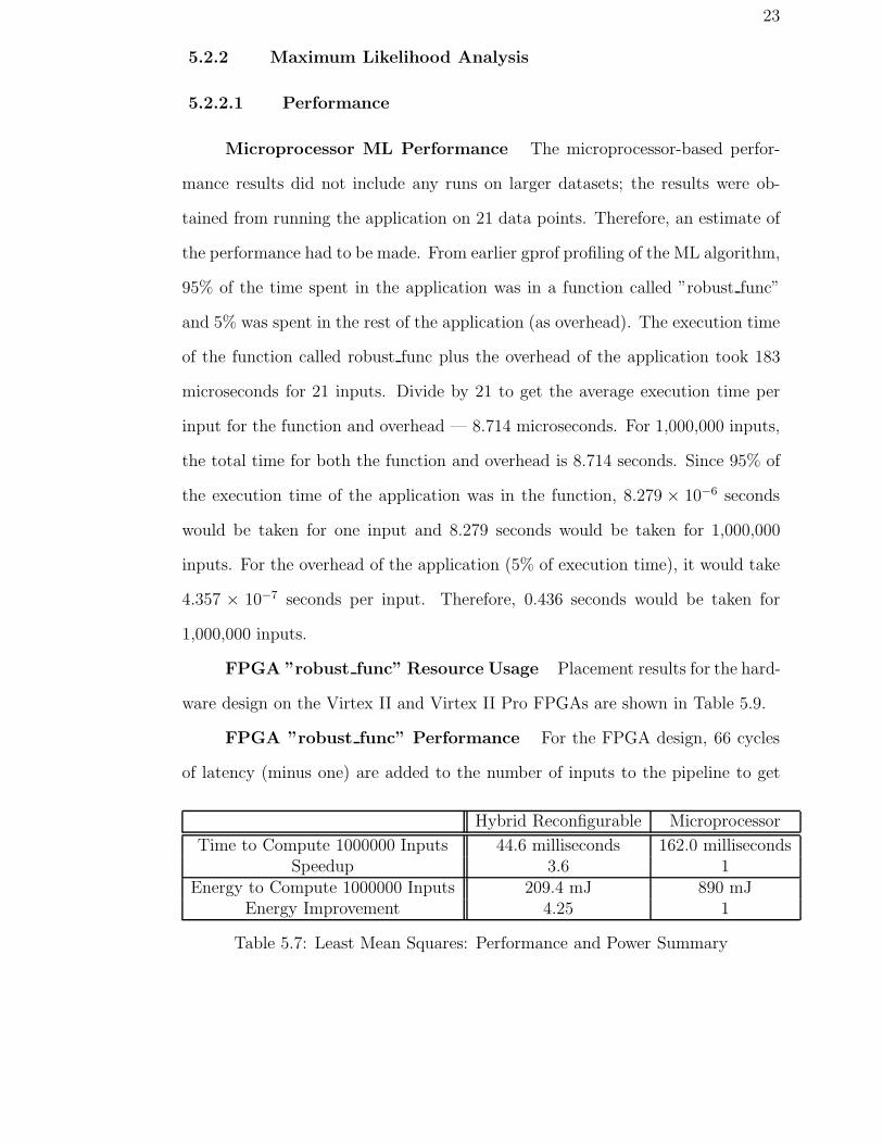
Microprocessor ML Performance The microprocessor-based perfor-
mance results did not include any runs on larger datasets; the results were ob-
tained from running the application on 21 data points. Therefore, an estimate of
the performance had to be made. From earlier gprof profiling of the ML algorithm,
95% of the time spent in the application was in a function called ”robust func”
and 5% was spent in the rest of the application (as overhead). The execution time
of the function called robust func plus the overhead of the application took 183
microseconds for 21 inputs. Divide by 21 to get the average execution time per
input for the function and overhead — 8.714 microseconds. For 1,000,000 inputs,
the total time for both the function and overhead is 8.714 seconds. Since 95% of
the execution time of the application was in the function, 8.279 × 10⁻⁶ seconds
would be taken for one input and 8.279 seconds would be taken for 1,000,000
inputs. For the overhead of the application (5% of execution time), it would take
4.357 × 10⁻⁷ seconds per input. Therefore, 0.436 seconds would be taken for
1,000,000 inputs.
FPGA ”robust func” Resource Usage Placement results for the hard-
ware design on the Virtex II and Virtex II Pro FPGAs are shown in Table 5.9.
FPGA ”robust func” Performance For the FPGA design, 66 cycles
of latency (minus one) are added to the number of inputs to the pipeline to get
Hybrid Reconfigurable Microprocessor
Time to Compute 1000000 Inputs 44.6 milliseconds 162.0 millisecondsSpeedup 3.6 1
Energy to Compute 1000000 Inputs 209.4 mJ 890 mJEnergy Improvement 4.25 1
Table 5.7: Least Mean Squares: Performance and Power Summary
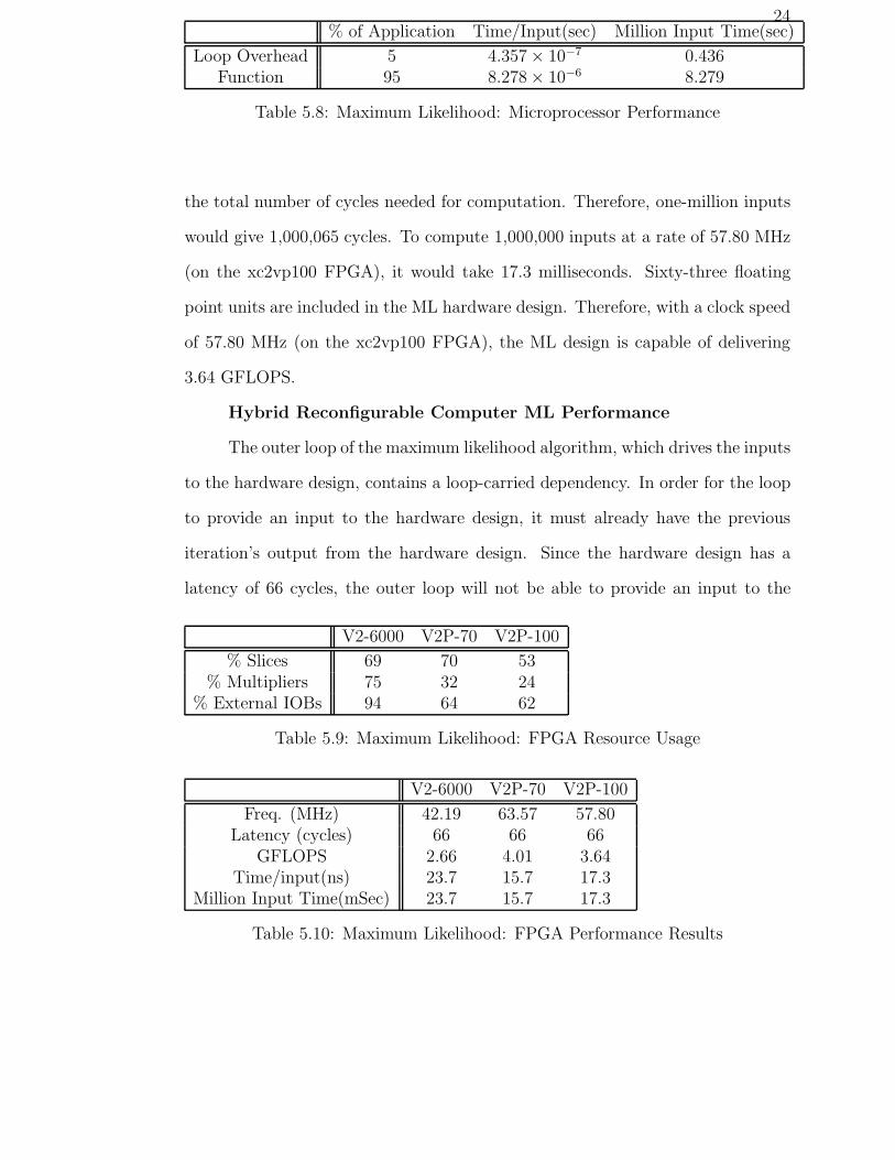
24% of Application Time/Input(sec) Million Input Time(sec)
Loop Overhead 5 4.357 × 10⁻⁷ 0.436Function 95 8.278 × 10⁻⁶ 8.279
Table 5.8: Maximum Likelihood: Microprocessor Performance
the total number of cycles needed for computation. Therefore, one-million inputs
would give 1,000,065 cycles. To compute 1,000,000 inputs at a rate of 57.80 MHz
(on the xc2vp100 FPGA), it would take 17.3 milliseconds. Sixty-three floating
point units are included in the ML hardware design. Therefore, with a clock speed
of 57.80 MHz (on the xc2vp100 FPGA), the ML design is capable of delivering
3.64 GFLOPS.
Hybrid Reconfigurable Computer ML Performance
The outer loop of the maximum likelihood algorithm, which drives the inputs
to the hardware design, contains a loop-carried dependency. In order for the loop
to provide an input to the hardware design, it must already have the previous
iteration’s output from the hardware design. Since the hardware design has a
latency of 66 cycles, the outer loop will not be able to provide an input to the
V2-6000 V2P-70 V2P-100
% Slices 69 70 53% Multipliers 75 32 24
% External IOBs 94 64 62
Table 5.9: Maximum Likelihood: FPGA Resource Usage
V2-6000 V2P-70 V2P-100
Freq. (MHz) 42.19 63.57 57.80Latency (cycles) 66 66 66
GFLOPS 2.66 4.01 3.64Time/input(ns) 23.7 15.7 17.3
Million Input Time(mSec) 23.7 15.7 17.3
Table 5.10: Maximum Likelihood: FPGA Performance Results
25
pipeline every cycle. Therefore, this application can’t utilize the pipeline.
To calculate the application performance of the hybrid reconfigurable sys-
tem, the loop overhead time of the microprocessor should be added to the amount
of time spent in the robust func hardware. We already have the loop overhead
time, which was computed in the microprocessor performance section. To cal-
culate the time spent in the robust func hardware, we notice that robust func is
called 22 times per iteration of the outside loop. Therefore, for each iteration of
the outside loop, the robust func hardware takes 2.512 × 10⁻⁵ seconds (22 calls
× 66 cycles/call × 17.3 ns/cycle (assuming the xc2vp100 FPGA)). The outside
loop iterates over each input, so 1,000,000 inputs give 25.12 seconds for the total
time of the robust func hardware. As stated before, the total time for the whole
application is equal to the loop overhead time plus the robust func hardware time,
for a total of 25.56 seconds for 1,000,000 inputs (assuming the xc2vp100 FPGA
is used).
5.2.2.2 Power
Microprocessor ML Power Again, due to the lack of RAD750 power
testing on large datasets, a power estimation had to be made. The microprocessor
took 1.02× 10⁻³ Joules to run the 21 input testbench; this number included both
the loop overhead and the function called ”robust func.” Divide the number by
21 to get the average energy consumed per input for the both the function and
overhead — 4.857×10⁻⁵ Joules. For 1,000,000 inputs, the total energy consumed
for both the function and overhead is 48.57 Joules. Since 95% of the application
was spent in the function, 4.614 × 10⁻⁵ Joules would be spent per input and
46.14 Joules would be spent for 1,000,000 inputs. The overhead of the application
(5%), 2.429 × 10⁻⁶ Joules would be spent per input. Therefore, it would take
2.429 Joules for 1,000,000 inputs.
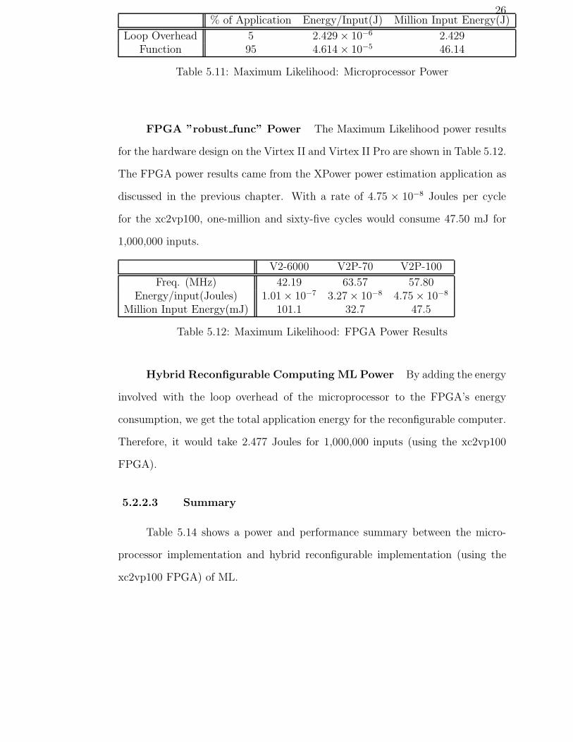
26% of Application Energy/Input(J) Million Input Energy(J)
Loop Overhead 5 2.429 × 10⁻⁶ 2.429Function 95 4.614 × 10⁻⁵ 46.14
Table 5.11: Maximum Likelihood: Microprocessor Power
FPGA ”robust func” Power The Maximum Likelihood power results
for the hardware design on the Virtex II and Virtex II Pro are shown in Table 5.12.
The FPGA power results came from the XPower power estimation application as
discussed in the previous chapter. With a rate of 4.75 × 10⁻⁸ Joules per cycle
for the xc2vp100, one-million and sixty-five cycles would consume 47.50 mJ for
1,000,000 inputs.
V2-6000 V2P-70 V2P-100
Freq. (MHz) 42.19 63.57 57.80Energy/input(Joules) 1.01 × 10⁻⁷ 3.27 × 10⁻⁸ 4.75 × 10⁻⁸
Million Input Energy(mJ) 101.1 32.7 47.5
Table 5.12: Maximum Likelihood: FPGA Power Results
Hybrid Reconfigurable Computing ML Power By adding the energy
involved with the loop overhead of the microprocessor to the FPGA’s energy
consumption, we get the total application energy for the reconfigurable computer.
Therefore, it would take 2.477 Joules for 1,000,000 inputs (using the xc2vp100
FPGA).
5.2.2.3 Summary
Table 5.14 shows a power and performance summary between the micro-
processor implementation and hybrid reconfigurable implementation (using the
xc2vp100 FPGA) of ML.
27
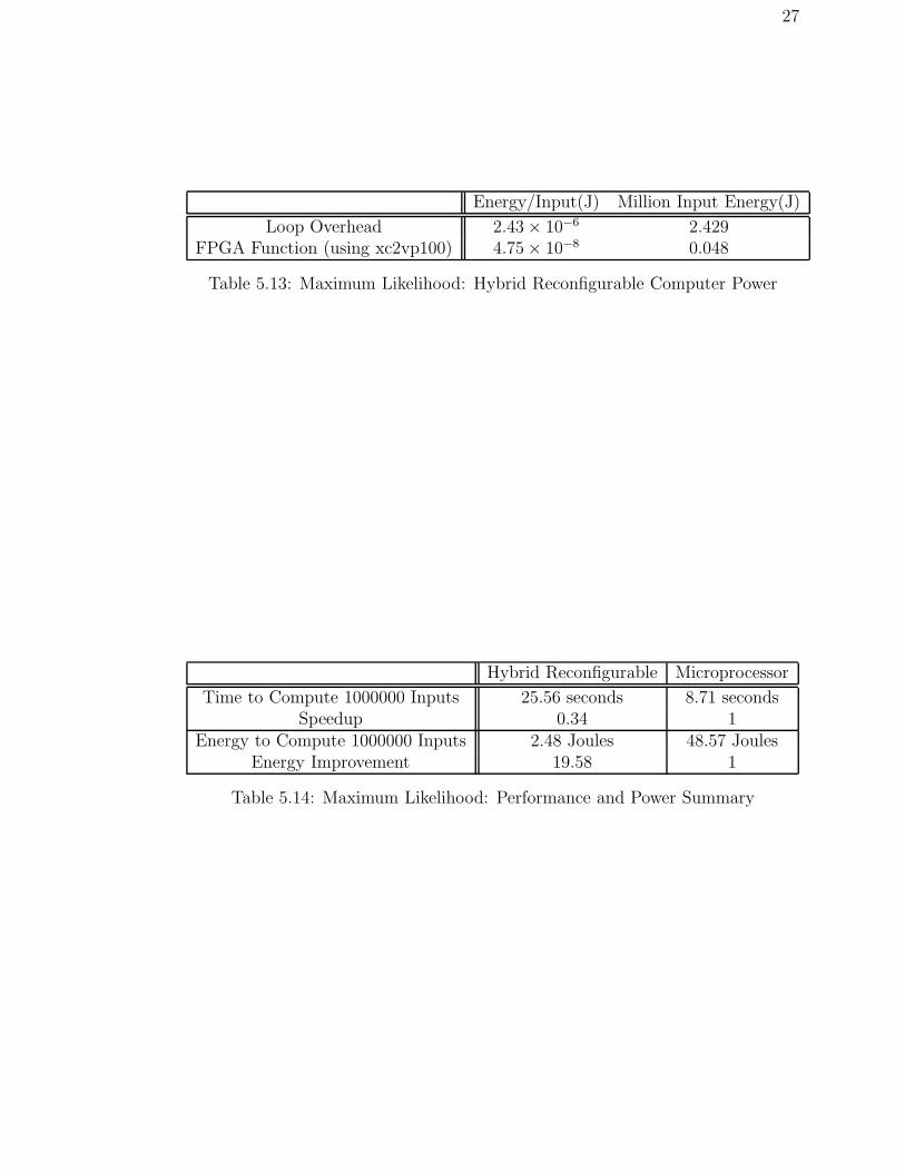
Energy/Input(J) Million Input Energy(J)
Loop Overhead 2.43 × 10⁻⁶ 2.429FPGA Function (using xc2vp100) 4.75 × 10⁻⁸ 0.048
Table 5.13: Maximum Likelihood: Hybrid Reconfigurable Computer Power
Hybrid Reconfigurable Microprocessor
Time to Compute 1000000 Inputs 25.56 seconds 8.71 secondsSpeedup 0.34 1
Energy to Compute 1000000 Inputs 2.48 Joules 48.57 JoulesEnergy Improvement 19.58 1
Table 5.14: Maximum Likelihood: Performance and Power Summary
Chapter 6
Conclusions
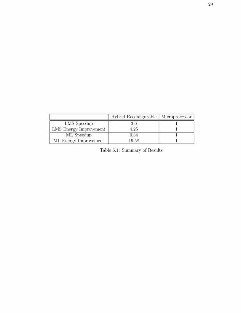
Table 6.1 shows a summary of power and performance results between the
hybrid reconfigurable computing implementation (using the xc2vp100 FPGA) and
the microprocessor implementation. This summary is based on an input stream
of 1,000,000 inputs, which would be likely for these signal processing applications.
Notice that the hybrid reconfigurable computing version of the LMS application
has both improved performance and energy consumption as compared to the mi-
croprocessor implementation. The reconfigurable computing version of the ML
application has improved energy consumption, but declined performance. The
main difference between these two reconfigurable applications is that the least
mean squares application was able to take full advantage of the hardware pipeline
while the maximum likelihood application was not.
These results suggest that it would be beneficial to use a reconfigurable
processing approach for the least mean squares computation. On the other hand,
the decision for the maximum likelihood application depends on whether power
or performance is more important for the space system. Also, one must take
into account the possibility of the hybrid reconfigurable computation of the ML
algorithm taking too long and interfering with the timely detection of ionospheric
events. If this occurred, the large power benefits associated with the reconfigurable
computing implementation of the ML application may not be important.
29
Hybrid Reconfigurable Microprocessor
LMS Speedup 3.6 1LMS Energy Improvement 4.25 1
ML Speedup 0.34 1ML Energy Improvement 19.58 1
Table 6.1: Summary of Results
Bibliography
[1] P. Belanovic and M. Leeser. A library of parameterized floating-point mod-ules and their use. In Proceedings of 12th International Conference onField-Programmable Logic and Applications. Springer-Verlag, 2002.
[2] W. Burleson, P. Jain, and S. Venkatraman. Dynamically parameterized ar-chitectures for power-aware video coding: Motion estimation and dct. InProceedings of Second International Workshop on Digital and ComputationalVideo (DCV’01). IEEE, 2001.
[3] S. Choi, R. Scrofano, V. Prasanna, and J. Jang. Energy-efficient sig-nal processing using fpgas. In FPGA’03, February 23-25, 2003, Monterey,California, USA. Association for Computing Machinery (ACM), 2003.
[4] J. Detrey and F. de Dinechin. Fplibrary, a vhdl library of parametrisablefloating-point and lns operators for fpga. 2004.
[5] M. Gokhale, J. Frigo, C. Ahrens, J. Tripp, and R. Minnich. Monte carloradiative heat transfer simulation on a reconfigurable computer. In FPL 2004:International Conference on Field-Programmable Logic and its Applications.Springer-Verlag, 2004.
[6] M. Gokhale, J. Stone, J. Arnold, and M. Kalinowski. Stream-oriented fpgacomputing in the streams-c high level language. In Proceedings of the IEEESymposium on Field-Programmable Custom Computing Machines (Napa,CA), 2000.
[7] G. Govindu, L. Zhuo, S. Choi, and V. Prasanna. Analysis of high-performancefloating-point arithmetic on fpgas. In Proceedings of the 18th InternationalParallel and Distributed Processing Symposium (IPDPS’04). IEEE Com-puter Society, 2004.
[8] BYU FPGA Reliability Group. Xpower studies.
[9] QinetiQ Holdings Ltd. Real time systems lab. 2002.
[10] Nallatech. Floating point ip cores for virtex-ii. 2003.
31
[11] K. Nichols, M. Moussa, and S. Areibi. Feasibility of floating-point arithmeticin fpga based artificial neural networks. CAINE02, 2002.
[12] W. Press, B. Flannery, S. Teukolsky, and W. Vetterling. Numerical Recipesin C: The Art of Scientific Computing. Cambridge University Press, secondedition edition, 1992.
[13] E. Roesler and B. Nelson. Novel optimizations for hardware floating-point units. In FPL 2002: The 12th International Conference onField-Programmable Logic and Applicatioins, pages 637–646. Springer-Verlag, 2002.
[14] I. Sahin, C. Gloster, and C. Doss. Feasibility of floating-point arithmetic inreconfigurable computing systems. In Military and Aerospace Applicationsof Programmable Devices and Technology Conference, 2000.
[15] P. Shriver, S. Briles, J. Harikumar, and M. Gokhale. A power-aware approachto processing payload design. In Proceedings of the Government MicrocircuitApplications and Critical Technology Conference (GOMACTech), 2003.
[16] P. Shriver, M. Gokhale, S. Briles, D. Kang, M. Cai, K. McCabe, S. Crago,and J. Suh. A power-aware, satellite-based parallel signal processing scheme.In Power Aware Computing. Kluwer Acedemic Press, 2002.
[17] K. Underwood. Fpgas vs. cpus: Trends in peak floating point performance.In FPGA’04, February 22-24, 2004, Monterey, California, USA. Associationfor Computing Machinery (ACM), 2004.
[18] X. Wang, M. Leeser, and H. Yu. A parameterized floating-point libraryapplied to multispectral image clustering. In 2004 MAPLD InternationalConference, September 8-10, 2004, Washington, D.C., 2004.