Embed Size (px)
Citation preview

ACM Transactions on Embedded Computing Systems, Vol. xx, No. x, Article x, Pub. date: xxx.
Reducing Leakage Power in Cache Peripheral Circuits of Embedded Processors HOUMAN HOMAYOUN COMPUTER SCIENCE AND ENGINEERING DEPARTMENT UNIVERSITY OF CALIFORNIA SAN DIEGO
ALEX VEIDENBAUM COMPUTER SCIENCE DEPARTMENT
UNIVERSITY OF CALIFORNIA IRVINE
AVESTA SASAN
BROADCOM CORPORATION, OFFIC OF CTO
DEAN TULLSEN COMPUTER SCIENCE AND ENGINEERING DEPARTMENT UNIVERSITY OF CALIFORNIA SAN DIEGO
________________________________________________________________________
Recent studies have shown that peripheral circuits, including decoders, wordline drivers, input and output
drivers, contribute a large fraction of the overall cache leakage. In addition, as technology migrates to smaller
geometries, leakage contribution to total power consumption increases faster than dynamic power, indicating that leakage will be a major contributor to overall power consumption. This paper proposes a combination of
circuit and architectural techniques to maximize leakage power reduction in embedded processors on-chip
caches by targeting leakage in cache peripheral circuits. At the circuit level, we propose a novel design with multiple sleep modes for cache peripherals. Each mode represents a trade-off between leakage reduction and
wakeup delay. Architectural control is proposed to decide when and how to use these different low-leakage
modes by utilizing cache miss information to guide its action. The control is based on simple state machines that do not impact area or power consumption and can thus be used even in resource-constrained processors.
Experimental results indicate that the proposed techniques can keep the data cache peripherals in one of the
low-power modes for more than 85% of total execution time. The instruction cache is in one of the low power modes for an average of 50% of the time. This translates to an average leakage power reduction of 50% for DL1
and 30% for IL1 in 65nm technology. The energy-delay product is reduced, on average, by up to 21%. The
overall processor power is reduced by up to 18% and by an average of 11% to 14%.
Categories and Subject Descriptors B.3.2 [MEMORY STRUCTURES], Design Styles: Cache memories; C.1.1 [PROCESSOR ARCHITECTURES], Single Data Stream Architectures: Pipeline processors Systems
General Terms: Design, Performance
Additional Key Words and Phrases: Cache, Leakage Power, Peripheral Circuits, Multiple Sleep Mode,
Embedded Processor
________________________________________________________________________
1. INTRODUCTION
Static or leakage energy consumption has been growing in both embedded and high-
performance processors as transistor geometries shrink. Cache and TLB RAM structures
account for a large fraction of processor power consumption [Rusu et al. 2007],
[Montanaro et al. 1996], and especially for leakage power. A number of process and
circuit techniques have been proposed to significantly reduce leakage of the memory cell
array making SRAM peripheral circuits the main sources of leakage. Recent results have
shown a large amount of leakage in the peripheral SRAM circuits, such as decoders,
word-line and output drivers [Homayoun et al. 2008], [Nakagome et al. 2003] [Takeyama
et al. 2006], [Gerosa et al. 2008], [Nii et al. 2004] [Mamidipaka et al. 2004]. For
instance, a wordline driver drives its signal to a large number of memory cells. To drive a

● H. Homayoun, A. Veidenbaum, A. Sasan and Dean M. Tullsen
ACM Transactions on Embedded Computing Systems, Vol. xx, No. x, Article x, Pub. date: xxx.
2
high capacitive load, a chain of tapered inverter buffers is used, typically with three to
five levels. We compare the leakage power consumption of a 65nm SRAM6T memory
cell1 with inverters of different size. The results are shown in Figure 1(a). It
Figure 1. (a) Leakage power dissipation of one SRAM6T memory cell compared with different size
inverter buffers (INVX is the smallest inverter buffer with drive strength of 1) (b) Leakage power
components for different cache size
shows that the leakage power of a standard memory cell is significantly lower than the
inverter buffer leakage and that the inverter leakage grows exponentially with its size.
Let us assume that a driver has to drive 256 one-bit memory cells. This will require three
stages of inverter buffers, with buffer size increasing by a factor of e in each additional
stage. The combined leakage power of these three drivers is 12 times larger than the
leakage of the 256 memory cells. In addition to the wordline driver, one has to consider
leakage in data input and output drivers, which are also high.
Two main reasons explain this difference in leakage:
Memory cells are designed with minimum-sized transistors mainly for area
considerations. Unlike memory cells, peripheral circuits use larger, faster and
accordingly, more leaky transistors so as to satisfy timing requirements [Nakagome
et al. 2003], [Mamidipaka et al. 2004].
Memory cells use high threshold voltage transistors, which have a significantly
lower leakage reduction compared with typical threshold voltage transistors used in
peripheral circuits [Takeyama et al. 2006], [Mamidipaka et al. 2004].
In summary, SRAM memory cells are optimized for low leakage current and area
without a significant impact on the cell performance [Nakagome et al. 2003], [Takeyama
et al. 2006], [Grossara et al. 2006], [Nii et al, 2004]. In addition, circuit techniques such
as gated-Vdd and drowsy cache can be applied to further reduce the memory cell leakage
and further widen the gap between the cell array and peripheral circuit leakage power
dissipation.
A similar result was obtained using CACTI 5.1 [Thoziyoor et al. 2008]. CACTI uses
characteristics of transistors modeled by the ITRS [Semiconductor Industries
Association, 2005]. It includes data for two device types that the ITRS defines - High
Performance (HP) and Low Standby Power (LSTP). The HP transistors are fast
transistors with short gate lengths, thin gate oxides, low Vth, and low Vdd. The LSTP
transistors, on the other hand, have longer gate lengths, thicker gate oxides, higher Vth,
and higher Vdd. As explained in [Nakagome et al. 2003], HP transistors are used in the
peripheral circuitry while LSTP transistors are used in the memory cell array. While it is
1 similar results were obtained for TSMC, TOSHIBA, IBM, UMC and CHARTERED foundries
using their libraries and evaluating leakage with SPICE.
0%
20%
40%
60%
80%
100%
2KB 4KB 8KB 16KB
data output driver
row pre/decoder and driver
data input driver
address input driver
others (sense amp, memory cell and etc)

Reducing Leakage in Data Cache Peripheral Circuits of Embedded Processors
ACM Transactions on Embedded Computing Systems, Vol. xx, No. x, Article x, Pub. date: xxx.
3
possible to use LSTP transistors in peripheral circuits for reducing leakage, the impact on
memory access time would be significant; for instance, it would result in an increase
from 1.3ns to 5.7ns in access time of a 16KB L1 cache. Figure 1(b) shows leakage
components for different size SRAMs in 65nm technology (based on CACTI 5.1
[Thoziyoor et al. 2008]), with peripheral circuits – data drivers, address driver, decoder
and wordline drivers – accounting for over 80% of overall SRAM leakage. Thus,
approaches that concentrate on cell leakage power alone are insufficient and it is very
important to address leakage in the peripheral circuits.
Since peripheral circuits use very large transistors to drive high loads to meet the
memory timing constraints, applying traditional leakage reduction techniques such as
“fine grained” sleep transistor insertion [Calhoun et al. 2003], [Khandelwal et al. 2004] in
these circuits could introduce significant area and delay overhead. This is mainly due to
the impact of leakage reduction techniques on peripheral circuits’ rise time, fall time,
propagation delay and area overhead [Homayoun et al. 2008]. These delays not only can
significantly increase the cache access time, but also require significant redesign and
verification efforts to avoid impacting memory functionality [Homayoun et al. 2008]. In
addition, peripheral circuits drive specific voltage levels and cannot be simply power-
gated. For instance, a word-line driver has to drive a Vlow voltage for all wordlines not
being accessed.
Therefore, the focus of this paper is on reduction of leakage-related power dissipation
in the on-chip SRAMs, targeting their peripheral circuits. The paper explores an
integrated circuit and architectural approach to reduce leakage in the cache peripherals. It
extends the work presented in [Homayoun et al. 2008], highlighting the importance of
leakage power reduction in cache peripherals, since they have the highest leakage energy
in the processors. There are a large variety of embedded processors, from single-issue, in-
order processors with one level of cache to multiple-issue, out-of-order processors with
two levels of cache. For this work we define the former as low-end embedded
processors, while a single-issue, in-order processor with two cache levels is defined as
high-end. The two types of embedded processors also differ in their clock speed. Our
goal is to explore leakage reduction in different levels of cache hierarchy. The same
techniques are applicable to out-of-order embedded processors that also offer other
opportunities for cache leakage reduction, but this type of processor is beyond the scope
of this paper.
At the circuit level, we utilize the recently proposed zig-zag share circuit [Homayoun
et al. 2008] to reduce the sub-threshold leakage in peripheral circuits of L1 caches (IL1
and DL1). The zig-zag horizontal and vertical share technique was shown to be vey
effective in reducing leakage of SRAM peripherals. The results in [Homayoun et al.
2008] showed leakage reduction by up to 100X in deeply pipelined SRAM peripheral
circuits, with only a minimal area overhead and small additional delay.
The wakeup latency of zig-zag share could be large, especially in large SRAMs, as
shown in [Homayoun et al. 2008]. To deal with this problem, this paper shows that by
increasing the gate bias voltage of the NMOS footer sleep transistor in the zig-zag share
circuit (and decreasing it for the PMOS header transistor) one can trade leakage reduction
for wakeup delay. Thus we propose to use several low-leakage modes with different
wakeup times to better control the cache leakage. For instance, one can have a low-
leakage mode for a DL1 cache with a one-cycle wakeup but it would reduce leakage by
only 40%. Alternatively, one can define a mode with a 4-cycle wakeup that saves 90% of
leakage. These modes differ only in how they bias sleep transistors and thus can be

● H. Homayoun, A. Veidenbaum, A. Sasan and Dean M. Tullsen
ACM Transactions on Embedded Computing Systems, Vol. xx, No. x, Article x, Pub. date: xxx.
4
dynamically switched during execution with almost no delay. We also propose a low-
power design for the bias generator circuit required for the multiple sleep modes
operation, shown to be fairly robust against six-sigma process, voltage and temperature
variations. In addition, we explore the design space of sleep transistor insertion in SRAM
peripheral circuitry and show the effect of sleep transistor size, its gate bias and the
number of horizontal and vertical levels of sharing on the leakage power savings,
instability, dynamic power, propagation delay, wakeup delay, rise time and fall time of
the SRAM peripheral circuits.
The next question is when and how to use these different low-leakage modes for L1
caches. Note that this approach can also be applied to L2 caches, but this is beyond the
scope of this paper. We propose architectural control of low-leakage modes in L1 caches.
The policy uses cache miss information to determine the mode. The action depends in
part on the cache organization and in part on the ability to hide the wakeup delay. In all
cases, control is based on simple state machines that do not impact area or power
consumption and can thus be used even in low-end processors. Hiding one to four cycles
of wakeup latency in a short pipeline typical of embedded processors is difficult to
accomplish in a uniform way, therefore we propose different methods for each delay and
low-leakage mode. For instance, one cycle of delay in DL1 access can be completely
hidden by starting cache wakeup as soon as instruction type is known in decode. Thus we
can actually keep the L1 cache peripherals in a basic low power mode with a one-cycle
wakeup as default. The most efficient low-energy mode with a four cycle wakeup delay
can be used during cache miss service. Other low-power modes can be used when an L2
cache is present.
The energy savings and performance of various cache configurations for embedded
processors are evaluated in this paper using the proposed circuit and architectural
techniques.
It is shown that our techniques can keep the data cache peripherals in one of the low-
power modes for more than 85% of total execution time, on average. The instruction
cache is in one of the low power modes for an average of 50% of the time. This translates
to an average leakage power reduction of 50% for DL1 and 30% for IL1 in 65nm
technology. The energy-delay product is reduced, on average, by up to 21%. The overall
processor power is reduced by up to 18.6% and by an average of 11% to 14%.
2. RELATED WORK
A number of techniques have been proposed for reducing leakage power at technology,
circuit, architecture and compiler/OS levels.
2.1 Circuit-Level Leakage Control
Several circuit techniques have been proposed to reduce the leakage power in SRAM
memories. These techniques mainly target the SRAM memory cell leakage.
The primary technique is voltage scaling which, due to short-channel effects in deep
submicron processes reduces the leakage current significantly [Flautner et al. 2002].
Another technique is Gated-Vdd which turns off the supply voltage of memory cells by
using a sleep transistor and eliminating the leakage almost completely [Powell et al.
2000]. However, it doesn't retain the state of the memory cells. The third technique,
ABB-MTCMOS, increases the threshold voltage of an SRAM cell dynamically through
controlling its body voltage [Nii et al. 1998]. The performance and area overhead of

Reducing Leakage in Data Cache Peripheral Circuits of Embedded Processors
ACM Transactions on Embedded Computing Systems, Vol. xx, No. x, Article x, Pub. date: xxx.
5
applying this technique makes it inefficient. Device scaling leads to threshold voltage
fluctuation, which makes the cell bias control difficult to achieve. In response,
[Takeyama et al. 2006] propose a Replica Cell Biasing scheme in which the cell bias is
not affected by Vdd and Vth of peripheral transistors.
[Agarwal et al. 2002] and [Kim et al. 2005] propose a forward body biasing scheme
(FBB) in which the leakage power is suppressed in the unselected memory cells of cache
by utilizing super Vt devices.
In addition to these four major techniques applied to SRAM memories, there are also
leakage reduction techniques in literature which concentrate on generic logic circuits.
Examples are sleepy stack [Park et al. 2006], sleepy keeper [Kim et al. 2006] and zig-zag
super cut-off CMOS (ZSCCMOS) techniques [Min et al. 2003], [Horiguchi et al. 1993].
ZSCCMOS reduces the wakeup overhead associated with the Gated-Vdd technique by
inserting the sleep transistors in a zig-zag fashion. Sleepy stack divides the existing
transistors into two half-size and then inserts sleep transistor to further reduce leakage.
This approach was shown to be area-inefficient as it comes with 50 to 120% area
overhead. Sleepy keeper is a variation of Gated-Vdd approach which can save logic state
during sleep mode. The drawback of this approach is significant additional dynamic
power overhead compare to the base circuit.
Optimal sizing of sleep transistors to minimize the impact of sleep transistor insertion
on the circuit delay has been researched extensively [Calhoun et al. 2003], [Mutoh et al.
1999], [Khandelwal et al. 2004], [Ramalingam et al. 2005]. [Mutoh et al. 1999] used the
average current consumption of logic gates to find the size of sleep transistor for
satisfying circuit speed. Their proposed technique is based on the assumption that the
circuit speed is weakly dependent on the circuit operating pattern for large enough sleep
transistor size.
2.2 Architectural Techniques
A number of architecturally driven cache leakage reduction techniques have been
proposed. Powell et al applied gated-Vdd approach to gate the power supply for cache
lines that are not likely to be accessed [Powell et al. 2000]. Kaxiras et al. propose a cache
decay technique which reduces cache leakage by turning off cache lines not likely to be
reused [Kaxiras et al. 2001]. Flautner et al. proposed a drowsy cache which reduces the
supply voltage of the L1 cache line instead of gating it off completely [Flautner et al.
2002]. The advantage of this technique is that it preserves the cache line information but
introduces a delay in accessing drowsy lines. Nicolaescu et al [Nicolaescu et al. 2006]
proposed a combination of way cache technique and fast speculative address generation
to apply the drowsy cache line technique to reduce both the L1 cache dynamic and
leakage power. [Zhang et al. 2002] proposed a compiler approach to turn off the cache
lines for a region of code that would not be accessed for a long period of time [Meng et
al. 2005]. Meng et al. presented a perfecting scheme which combines the drowsy caches
and the Gated-Vdd techniques to optimize cache leakage reduction [Meng et al. 2005]. Ku
et al. [Ku et al. 2006] exploit several power density minimization techniques to reduce
temperature and further leakage in highly-associative

● H. Homayoun, A. Veidenbaum, A. Sasan and Dean M. Tullsen
ACM Transactions on Embedded Computing Systems, Vol. xx, No. x, Article x, Pub. date: xxx.
6
slpN
vss
N
MV
vdd
gnV
gslpnV vss
LC
CV
(a)
vddvdd vdd vdd
z
BitlineBitlineP1 P2
N1 N2
vssvss
010
I leakage
I leakage
5.1L
W
3L
W
3L
W
6L
W
P3
N3
vss
6L
W
12L
W
vss
01
12L
W
24L
W
addr0
addr1
addr2
addr3
N4
P4
(b)
Figure 2. (a) Stacking sleep transistor to reduce leakage (b) Leakage in the wordline driver
on-chip caches in embedded processors. Due to the positive feedback relation of
temperature and leakage, they show on-chip cache leakage reduces significantly.
In a recent work, Chun et al. proposed a novel approach, which utilizes branch
prediction assist to selectively wake up only the needed instruction cache line for an
embedded processor [Chun et al. 2008].
All research mentioned above primarily targets the leakage in the SRAM cells of a
cache. Given the results in Figure 1 and in [Homayoun et al. 2008], [Gerosa et al. 2008],
[Takeyama et al. 2006], [Nii et al. 2004] and [Mamidipaka et al. 2004], peripheral
circuits are equally if not more important to address in a cache.
3. SLEEP TRANSISTOR STACKING
Stacking sleep transistors have been proposed to reduce sub-threshold (IDsub) or weak
inversion current [Kao et al. 1998]. IDsub is an inverse exponential function of threshold
voltage (TV ). Threshold voltage is a function of Source to Bulk Voltage. An effective
way to reduce the leakage of a transistor is by increasing its source voltage (for an NMOS
increasing VSB, the source to bulk voltage) [Kao et al. 1998], [Rabaey et al. 2003].
Stacking a sleep transistor (footer NMOS or header PMOS transistor) as shown in
Figure 2(a) could deliver this effect. In this figure by stacking transistor N with slpN
source to body voltage (VM ) of transistor N increases. When both transistors are off an
increase in VM increases the TV of the transistor N and therefore reduces sub-threshold
leakage current [Kao et al. 1998]. Size (W/L) and bias (Vgslpn) voltage of the stacked
sleep transistor determines the VM [Agarwal et al. 2006], [Kao et al. 1998]. Reducing the
sleep transistor bias reduces the leakage while increasing the circuit wakeup period which
is the time to pull the VM down to ground. Thus there is a trade-off between the amount
of leakage saved and the wakeup overhead [Agarwal et al. 2006].

Reducing Leakage in Data Cache Peripheral Circuits of Embedded Processors
ACM Transactions on Embedded Computing Systems, Vol. xx, No. x, Article x, Pub. date: xxx.
7
A wordline driver shown in Figure 2(b) increases the gate voltage of the access
transistors of all cells connected to the selected wordline. The number and size of
inverters in the chain are chosen to meet the timing requirements for charging or
discharging the wordline (usually the number of inverter stages varies from two to five.
For this particular example we assumed four stages. Based on our experimental results
the relative leakage power consumption does not change noticeably for our case,
compared to a design with fewer or more inverter stages). The size of inverters in the
chain decreases from decoder side to the wordline to increase the effective fan-out. The
inverter chain has to drive a logic value 0 to the pass transistors when a memory row is
not selected. Thus the driver cannot be simply shut down when idle. Transistors N1, N3
and P2, P4 are in the off state and thus they are leaking.
Stacking header and footer sleep transistors with all NMOS and PMOS transistors in
the chain reduces their leakage; however, aside from the area overhead, it increases the
propagation delay of the inverters in the driver chain followed by an increase in the
rise/fall time of the wordline. Rise and fall time of an inverter output is proportional to
Rpeq * CL and Rneq * CL, respectively, where Rpeq is the equivalent resistance of the
PMOS transistor, Rneq is the equivalent resistance of the NMOS transistor, and CL is the
equivalent wordline output capacitive load [Rabaey et al. 2003]. Inserting sleep
transistors increases Rneq, Rpeq and thus the rise time and fall time of the wordline driver
as well as its propagation delay [Homayoun et al. 2008], [Rabaey et al. 2003]. Increase in
rise and fall times and propagation delay is not desirable, as the memory functionality
and access time are negatively affected [Amrutur et al. 2000], [Mai et al. 1998], [Margala
et al. 1999]. Any increase in the fall time of wordline driver results in an increase in pass
transistor active period during a read operation. This results in the bit-line over-discharge
and the memory content over-charge during the read operation. Such over-discharge not
only increases the dynamic power dissipation of bit-lines, more importantly, it can cause
a memory cell content to enter a metastable state if the over-discharge period is large
[Amrutur et al. 2000], [Mai et al. 1998], [Margala et al. 1999]. In addition, such increase
in pass transistors active period requires re-timing of the sense amplifier active period.
Note that it is typical in low power SRAM memories to use a self-timed clocked sense
amplifier to limit sense power and track the bit-line delay to setup the sense amplifier in
the high gain region for sensing right before the pass transistors are turned off. Such a
self-timed clocked sense amplifier has to cope with any increase in the pass transistor M1
active period [Amrutur et al. 2000], [Mai et al. 1998]. In brief, to avoid impacting
memory functionality the sense amplifier timing circuit and the wordline pulse generator
circuit need to be redesigned. To avoid the redesign of these critical units and, moreover,
not to increase bitline dynamic power dissipation we use zig-zag share circuit technique
proposed in [Homayoun et al. 2008].
3.1 Zig-Zag Share Circuit
In this approach, sleep transistors are inserted in a zig-zag fashion [Min et al. 2003],
[Horiguchi et al. 1993] keeping the Rpeq of the first and third inverters and Rneq of the
second and fourth inverters constant. This technique keeps the fall time of the circuit the
same as in the baseline circuit with no leakage control. However, the rise time of the
circuit is affected by the zig-zag scheme. In addition, using one sleep transistor per
inverter logic increases the area for the zig-zag scheme.

● H. Homayoun, A. Veidenbaum, A. Sasan and Dean M. Tullsen
ACM Transactions on Embedded Computing Systems, Vol. xx, No. x, Article x, Pub. date: xxx.
8
To improve both leakage reduction and area-efficiency of the zig-zag scheme,
[Homayoun et al. 2008] proposed using one set of sleep transistors shared between
multiple stages of inverters which have similar logic behavior, such as stage 1 and 3 in a
vdd vdd vddvdd vdd
vss vss vss vss vss
slpN
slpPSleep signal
Sleep signal
P11 P12 P13 P14P21 P22 P23 P24
N11 N12 N13 N14N21 N22 N23 N24
Word-line
Driver line K
Word-line
Driver line K+1
MV
Figure 3.Zig-zag horizontal and vertical sharing circuit
studied chain of inverters. To further reduce leakage power, [Homayoun et al. 2008]
proposed to also share one set of sleep transistors (slpN and slpP) vertically with adjacent
rows of (wordline) drivers.
Figure 3 shows the zig-zag horizontal and vertical sharing circuit (in brief ZZ-HVS)
when two adjacent wordline drivers share one set of sleep transistors. Intuitively, in
vertical sharing (for instance for N11 and N21), the virtual ground voltage (VM in Figure 3)
increases in comparison to when there is no vertical sharing.
Results in [Homayoun et al. 2008] show that using ZZ-HVS reduces the leakage power
significantly, by 10 to 100X, when 1 to 10 wordlines share the same sleep transistors.
4. ZIGZAG-SHARE WITH MULTIPLE SLEEP MODES
As explained in Section 3, to maximize the benefit from the leakage savings of stacking
sleep transistors we need to keep the bias voltage of the NMOS footer sleep transistor as
low as possible (and for the PMOS header transistor as high as possible). The drawback
of such biasing is its impact on wakeup latency and wakeup power of the circuit
transitioning from sleep mode to active mode, which requires the voltage of virtual
ground to reach the true ground. Such wakeup delay and its wakeup power overhead
could significantly impact performance and diminish the power savings if incurred
frequently. Appropriately sizing a sleep transistor (both footer and header) [Agarwal et al.
2006] and controlling its bias voltage are two effective ways to minimize the impact on
wakeup delay and wakeup power overhead. For instance, increasing the gate voltage of
the footer sleep transistor (in Figure 2(a)) reduces the virtual ground voltage (VM), which
subsequently reduces the circuit wakeup delay and wakeup power overhead. The negative
impact of such biasing is a reduction in leakage power savings. To better explain this, let
us examine the wakeup delay and wakeup power overhead as a function of sleep
transistor size and its gate bias voltage.
The wakeup delay and power overhead are measured as the time and power required
for the virtual ground voltage (VM in Figure 2(a)) to be discharged through a sleep
transistor to reach the ground level [Amrutur et al. 2000]. This wakeup delay is expressed
as follows:

Reducing Leakage in Data Cache Peripheral Circuits of Embedded Processors
ACM Transactions on Embedded Computing Systems, Vol. xx, No. x, Article x, Pub. date: xxx.
9
2
2
1Mblockwakeup VCE Equation 1
vdd
vss
M2
vdd
vss
M1
M4M3
M6M5
M8M7
Vref
Figure 4. A robust gate bias generator circuit.
slp
blockMwakeup
I
CVT
Equation 2
where Cblock is the total capacitance of the circuit block and slpI is the current of the sleep
transistor after it is turned on to wake up the block. Such wakeup overhead is decided by
the equivalent load, as shown in EQ.1.
As shown in [Agarwal et al. 2006], the virtual ground voltage is linearly dependent on
the sleep transistor gate voltage; increasing the gate voltage of the NMOS sleep transistor
reduces VM. According to EQ.1 and EQ.2, such reduction reduces the wakeup delay and
wakeup power overhead.
Also as discussed in Section 3, increasing the gate voltage of the sleep transistor results
in higher leakage power dissipation. In fact, by controlling the gate voltage of the footer
and header transistors we can define different sleep modes where each mode has a
different wakeup delay overhead and a different amount of leakage power reduction. We
refer to this scheme as multiple sleep modes zig-zag horizontal and vertical sharing or in
brief MZZ-HVS.
4.1 The Bias Generator
As described in the previous section, the benefit of multiple sleep modes is obtained by
controlling the gate voltage of the sleep transistor. A stable and robust voltage reference
generator is needed to ensure the performance of multiple sleep mode operation over
process, voltage, and temperature variations.
A Conventional bandgap reference circuit consists of bipolar transistors and resistors
that might occupy a noticeable amount of area. A CMOS voltage reference in Figure 4
consisting of transistors in saturation, triode, and subthreshold regions can provide sub-1-
V reference required in our design. Transistors M1 – M4 in Figure 4 are always in
saturation and generate supply independent current. Transistors M5 and M6 operate in
the triode region as voltage controlled resistors and produce PTAT (Proportional to
Absolute Temperature) voltage. Transistors M7 and M8 operate in the subthreshold
region, behaving as bipolar transistors to produce CTAT (complementary to absolute
temperature) voltage.

● H. Homayoun, A. Veidenbaum, A. Sasan and Dean M. Tullsen
ACM Transactions on Embedded Computing Systems, Vol. xx, No. x, Article x, Pub. date: xxx.
10
Figure 5. Reference voltage versus temperature in C.
Figure 6. Wakeup delay and leakage power for different footer and header gate bias voltage pairs
The reference voltage is taken from the drain node of M6. Figure 5 shows the
simulation results of reference voltage versus temperature from -40C to 125C, where
only ±1.6% voltage variation around the nominal value is observed across this wide
temperature range.
5. CIRCUIT EVALUATION
The proposed multiple sleep mode zig-zag share approach was applied to SRAM
wordline drivers. A test experiment was set up in which the wordline inverter chain
drives 256 one-bit memory cells. The memory cells and wordline drivers were laid out
using Mentor Graphic IC-Station in a 65nm technology and simulated using Synopsis
Hspice at typical corner (25 º) with extracted netlist and the supply voltage of 1.08V.
Empirical results presented are for leakage power and wakeup delay for different pairs of
sleep transistors’ bias voltage.
Figure 6 shows normalized wakeup delay and normalized leakage power for different
footer and header gate bias voltage pairs when ZZ-HVS is shared by 10 rows of wordline
drivers. The figure shows a clear trade-off between the wakeup overhead and leakage
power. Increasing the bias voltage of the footer transistor reduces the leakage power
savings as well as the wakeup delay. 5.1 Impact of Sleep Transistor sizing on Leakage Power Reduction/Wakeup Delay and Propagation Delay
As discussed in Section 3, inserting sleep transistors in a zig-zag share fashion increases
the circuit propagation delay as well as its rise time. Appropriately sizing the sleep
transistor can minimize the impact on circuit propagation delay as well as on its rise time.
0.280
0.285
0.290
0.295
0.300
0.305
0.310
-40
-30
-20
-10 0 10 19 29 39 49 59 69 79 89 99 109
118
Temperature
Ref
eren
ce V
olt
age
1.0
1.5
2.0
2.5
3.0
3.5
4.0
4.5
5.0
(0,1
)
(0.0
5,.9
6)
(0.1
,0.9
3)
(0.1
5,0.
89)
(0.2
0,0.
85)
(0.2
5,0.
80)
(0.3
0,0.
75)
(Footer,Header) Gate Bias Voltage Pair
No
rmalized
Leakag
e P
ow
er
0.2
0.3
0.4
0.5
0.6
0.7
0.8
0.9
1
No
rmalized
Wake-U
p D
ela
yNormalized leakage Normalized wake-up delay

Reducing Leakage in Data Cache Peripheral Circuits of Embedded Processors
ACM Transactions on Embedded Computing Systems, Vol. xx, No. x, Article x, Pub. date: xxx.
11
Assume that a % increase in the wordline driver propagation delay is tolerable. Now
let’s find the appropriate size of sleep transistor so that the propagation delay does not
increase beyond %. Delay of a gate without sleep transistor is expressed as:
tlDD
DDLd
VV
VCT Equation 3
Delay of a gate with sleep transistor is expressed as,
tlxDD
DDLdsleep
VVV
VCT Equation 4
CL is the load capacitance at the gate’s output, Vtl is the threshold voltage of the inverter
chain.
With a % delay overhead allowed during active operation of the word line driver,
)100
1(
dsleep
d
T
T Equation 5
tlDDx VVV )1)100
1((
Equation 6
2
2x
xthDD
sleep
oxnsleep
VVVV
L
WCI Equation 7
For the word line driver, Vtl is the same as Vth of sleep transistor.
2
2
2
)1)100
1(
)1)100
1( thDD
sleep
sleep VVL
WoxCnI
Equation 8
Figure 7. Impact of sleep transistor sizing on propagation delay
0.90
0.95
1.00
1.05
1.10
1.15
1.20
W(1X) W(2X) W(3X) W(4X) W(5X) W(6X) W(7X) W(8X)
sleep transistor relative size
Re
lati
ve
Pro
pa
ga
tio
n D
ela
y
● H. Homayoun, A. Veidenbaum, A. Sasan and Dean M. Tullsen
ACM Transactions on Embedded Computing Systems, Vol. xx, No. x, Article x, Pub. date: xxx.
12
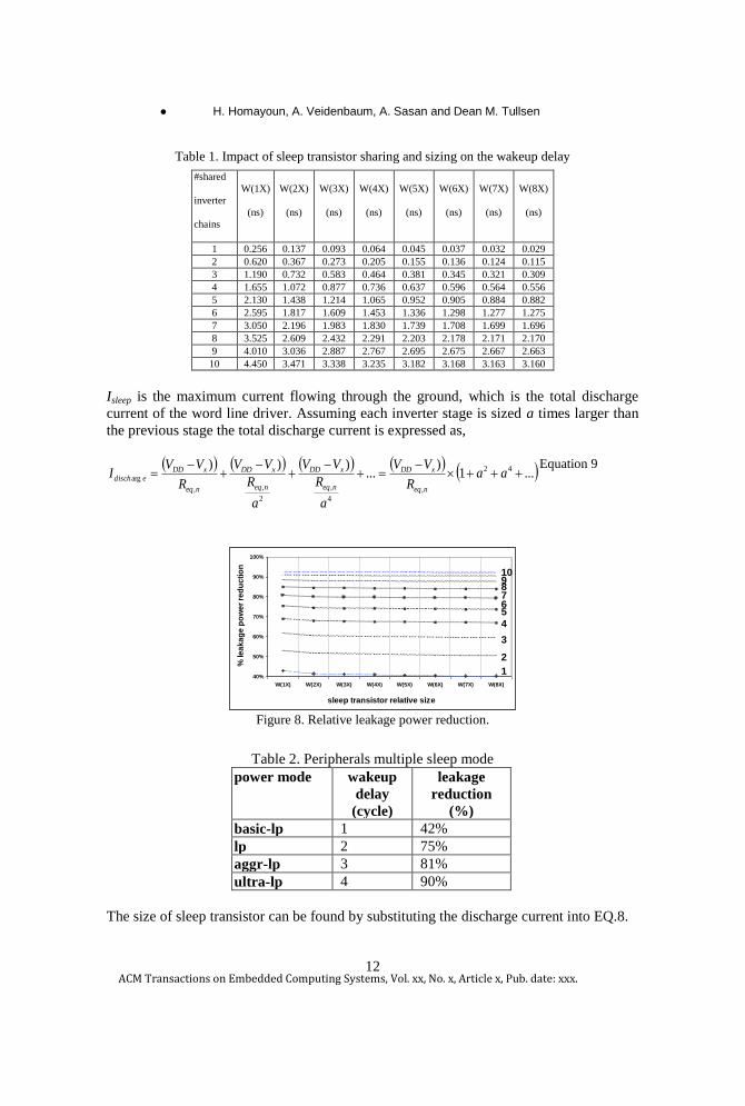
Table 1. Impact of sleep transistor sharing and sizing on the wakeup delay
#shared
inverter
chains
W(1X)
(ns)
W(2X)
(ns)
W(3X)
(ns)
W(4X)
(ns)
W(5X)
(ns)
W(6X)
(ns)
W(7X)
(ns)
W(8X)
(ns)
1 0.256 0.137 0.093 0.064 0.045 0.037 0.032 0.029
2 0.620 0.367 0.273 0.205 0.155 0.136 0.124 0.115
3 1.190 0.732 0.583 0.464 0.381 0.345 0.321 0.309
4 1.655 1.072 0.877 0.736 0.637 0.596 0.564 0.556
5 2.130 1.438 1.214 1.065 0.952 0.905 0.884 0.882
6 2.595 1.817 1.609 1.453 1.336 1.298 1.277 1.275
7 3.050 2.196 1.983 1.830 1.739 1.708 1.699 1.696
8 3.525 2.609 2.432 2.291 2.203 2.178 2.171 2.170
9 4.010 3.036 2.887 2.767 2.695 2.675 2.667 2.663
10 4.450 3.471 3.338 3.235 3.182 3.168 3.163 3.160
Isleep is the maximum current flowing through the ground, which is the total discharge
current of the word line driver. Assuming each inverter stage is sized a times larger than
the previous stage the total discharge current is expressed as,
...1
)...
))) 42
,
4
,
2
,,
arg
aaR
VV
a
R
VV
a
R
VV
R
VVI
neq
xDD
neq
xDD
neq
xDD
neq
xDDedisch
Equation 9
Figure 8. Relative leakage power reduction.
Table 2. Peripherals multiple sleep mode
power mode wakeup
delay
(cycle)
leakage
reduction
(%)
basic-lp 1 42%
lp 2 75%
aggr-lp 3 81%
ultra-lp 4 90%
The size of sleep transistor can be found by substituting the discharge current into EQ.8.
40%
50%
60%
70%
80%
90%
100%
W(1X) W(2X) W(3X) W(4X) W(5X) W(6X) W(7X) W(8X)
sleep transistor relative size
% le
ak
ag
e p
ow
er
red
uc
tio
n
1
2
3
5
4
678910

Reducing Leakage in Data Cache Peripheral Circuits of Embedded Processors
ACM Transactions on Embedded Computing Systems, Vol. xx, No. x, Article x, Pub. date: xxx.
13
2
2
arg
2
)1)100
1(
)1)100
1( thDDox
edisch
sleep
VVCn
I
L
W
Equation 10
The impact of sleep transistor sizing on propagation delay for ZZ-HVS circuit when 10
rows of wordline drivers share sleep transistor is shown in Figure 7. Increasing the size of
sleep transistor reduces the propagation delay overhead, for instance increasing the size
of sleep transistor by 8X reduces the impact on propagation delay from 10% down to
near 1%.
Table 1 reports the impact of sleep transistor sharing and sizing on wakeup delay when
each wordline drives 256 one-bit memory cells. Higher degree of sharing of the sleep
transistor results in larger wakeup delay. Increasing the size of the sleep transistor
reduces the wakeup delay. Increasing the number of shared wordlines reduces the benefit
of using a larger sleep transistor on wakeup delay reduction.
Figure 8 reports the relative leakage power reduction as a function of sleep transistor
size and the number of sharing inverter chains. These results show that the sleep
transistor size has a small impact on leakage power savings.
Finally, note that the power overhead of waking up peripheral circuits from any low
power mode is negligible, almost equivalent to the switching power of sleep transistors.
Sharing a set of sleep transistors horizontally and vertically for multiple stages of
(wordline) drivers makes the power overhead even smaller.
6. APPLYING ZZ-HVS TO L1 DATA AND INSTRUCTION CACHES
Some of the highest leakage units in the processor are the on-chip caches (such as L1 and
L2). Thus, it makes a lot of sense to apply the ZZ-HVS circuit technique to these units.
Note that we assume the small impact of ZZ-VHS on propagation delay (1%) can be
tolerated and hidden in deep pipeline memories such as L1 cache and thus it does not
degrade their operating frequency.
As explained above, there is a latency associated with waking up the SRAM peripheral
circuitry. The overall time delay for transition to/from the standby mode, STL, is the sum
of sleep transistors wakeup delay and a propagation delay of the sleep signal. Both of
these delays increase as the memory area increases, especially the latter delay, because
the sleep signal needs to be transmitted over a greater distance. Accordingly, depending
on the memory size and configuration, there is a different wakeup delay overhead for a
specific ZZ-HVS bias voltage. To find the STL delay for an SRAM array, SPICE and a
modified version of CACTI were used to measure the wakeup delay of a sleep transistor
and the propagation delay of the sleep signal, respectively. To estimate the propagation
delay we assumed that the sleep signal has to be transmitted across the SRAM
peripherals. Based on these experimental results different sleep modes were defined for
DL1 and IL1 caches. Table 2 shows wakeup delay and relative peripheral circuit leakage
reduction for these four different modes. The basic low power mode has the lowest
leakage reduction but shortest wakeup delay. Next is lp mode which has higher leakage

● H. Homayoun, A. Veidenbaum, A. Sasan and Dean M. Tullsen
ACM Transactions on Embedded Computing Systems, Vol. xx, No. x, Article x, Pub. date: xxx.
14
savings. Aggressive and ultra sleep modes have even higher leakage savings but also a
longer wakeup delay.
This section describes the architectural approach to control the ZZ-HVS sleep
transistors in DL1 and IL1 caches2 for two different types of embedded processors: a
low-end and a high-end. We start by briefly describing the processor architectures and the
experimental methodology used and then present results for different cache
organizations.
6.1 Experimental Methodology
The approach proposed in this paper was evaluated for several processor architectures
(shown in Table 3) which differ primarily in their memory hierarchy. A low-end
processor uses 2, 4, 8 or 16KB L1 instruction and data caches and no L2 cache. The high-
end processor has two levels of on-chip caches, with L1 cache size of up to 32KB. The
rest of the processor architecture is similar to the ARM11 family of processors [ARM11
MPCore Processor].
Figure 9 shows the processor pipeline of ARM11, a single issue, out of order
completion processor. It has two fetch stages and two stages for data cache access. The
fetch stages fill a four-entry instruction fetch buffer [ARM11 MPCore Processor].
fetch1 fetch2
Instruction cache
access and branch
prediction
DecodeIssue
Register
file
access
Load/
store
Data Cache Access
Write
buffer
external
Write
buffer
shift ALU SAT
MAC1 MAC2 MAC3
DC-1 DC-2
Figure 9. ARM11 processor pipeline
Table 3. Processor Architecure Configurations
Low-end configuration High-end
configuration L1 I-cache 2-4-8-16KB, 4 way, 2 cycles
4-8-16-32KB, 8 way, 2 cycles L1 D-cache 2-4-8-16KB, 4 way, 2
cycles
4-8-16-32KB, 8 way 2 cycles L2-cache none 64-128-256-512KB, 15 cycles Fetch, dispatch 1 wide 1 wide Issue in-order, non blocking in-order, non blocking Memory 30 cycles 80 cycles Instruction fetch queue 4 4 Load/store queue 4 entry 8 entry Arithmetic units 1 integer, 1 f.p. 1 integer, 1 f.p. Complex unit 1 integer, 1 f.p.
multiply/divide
1 integer, 1 f.p. multiply/divide Pipeline 8 stages 8 stages
2 While it is possible to apply ZZ-HVS to other SRAM units such as the register file, reorder
buffer, L2 cache, instruction cache, branch predictor, DTLB and ITLB, this paper studies the
application in DL1 and IL1 cache only.

Reducing Leakage in Data Cache Peripheral Circuits of Embedded Processors
ACM Transactions on Embedded Computing Systems, Vol. xx, No. x, Article x, Pub. date: xxx.
15
Clock speed 300 MHz 800 MHz
The processor supports non-blocking and hit-under-miss operations in which it
continues execution after a cache miss, as long as subsequent instructions are not
dependent on cache miss data. The processor pipeline stalls only after three successive
data cache misses.
An extensively modified MASE [SimpleScalar 4] simulator was used to model the
architecture. The MiBench suite [MiBench Version 1.0] was used to represent a (low-
end) embedded domain. SPEC2K benchmarks were used for the high-end processor. All
benchmarks were compiled with the -O4 flag using the Compaq compiler targeting the
Alpha 21264 processor. MiBench benchmarks executed for 500 Million instructions and
SPEC2K for 500 Million instructions after fast-forwarding for 500 Millions instructions.
6.2 Reducing Leakage in L1 Data Cache
One approach to maximize leakage reduction in DL1 cache peripherals is to always keep
them in ultra low power mode. However, this requires wakeup of DL1 peripheral circuits
before each cache access and adds 4 cycles to the DL1 latency, which significantly
reduces performance. One can put DL1 peripherals into the basic low power mode, which
requires only one cycle to wakeup, and possibly even hide this wakeup latency, thus not
degrading performance. However, this doesn’t reduce leakage power significantly (see
Table 2). To benefit from the large leakage reduction of ultra and aggressive low power
modes while attaining the low performance impact of the basic-lp mode one has to
dynamically change the peripheral circuit sleep modes. They should be kept in basic-lp
mode during periods of frequent access and transitioned to aggr-lp or ultra-lp modes
when accessed infrequently. The question is how to control such low-power mode
transitions.
In this architecture it is known whether an instruction is a load or a store at least one
cycle before cache access (during issue stage in Figure 9). As a result, DL1 peripheral
circuits can be woken up one cycle prior to access. Thus there is no impact on DL1
access latency when its peripherals are in basic-lp mode. Similarly, one cycle of the
wakeup delay can be hidden for all other low-power modes. Thus the effective wakeup
delay of the DL1 cache is one cycle less than the delays shown in Table 2.
In addition, the following behavior of DL1 cache access has been observed and will be
used to guide mode transitions. For low-end processors the DL1 is accessed infrequently,
if at all, when there is one or more pending DL1 cache misses. Thus it can be put into
ultra low power mode during miss service. For high-end processors the DL1 is accessed
very infrequently while an L2 cache miss is being serviced. It is also access infrequently
with no L2 cache misses but with multiple outstanding L1 misses and can be kept in
aggressive low power modes.
Based on the above, the DL1 is kept in the basic-lp mode by default. The following
state machines are proposed for controlling low-power mode transitions for different
cache configurations.
6.2.1 Low-end architecture For low-end architectures, the state machine shown in Figure 10(a) is proposed for
controlling the DL1 low-power mode. Once a DL1 cache miss occurs the peripheral
circuits transition from basic to lp mode. Given the miss service time of 30 cycles in this
architecture, it is likely that the processor stalls during the miss service period.
Occurrence of additional cache misses while one DL1 cache miss is already pending

● H. Homayoun, A. Veidenbaum, A. Sasan and Dean M. Tullsen
ACM Transactions on Embedded Computing Systems, Vol. xx, No. x, Article x, Pub. date: xxx.
16
further increases the chance of pipeline stall. Thus the DL1 peripherals are put into the
aggressive low-power mode with more leakage savings.
Finally, the cache peripherals are put into the deepest low power mode, ultra-lp, once
the processor stalls after DL1 misses occurs. A stall is detected in the issue stage and the
processor put into ultra-lp when the processor does not issue any instructions for five
consecutive cycles after a DL1 miss.
The processor returns to the basic-lp mode from any of the other low power states
when one of the two following conditions are met:
Stall condition removed; i.e instruction issue resumes
All pending DL1 misses are serviced
Figure 11(a) reports the fraction of total execution time a 2KB DL1 cache spends in
each of the power modes for the MiBench benchmarks. On average, 85% of the time
DL1
basic-lp lp ultra-lp
aggr-lp
DL1 miss
Processor stall
DL1 miss++
Pending DL1
miss
Pending DL1
miss/es
Processor stallall DL1 misses serviced
DL1 miss
serviced
Processor continue
(a)
basic-lp lp ultra-lpDL1 miss
L2 miss
Pending DL1
miss/esDL1 miss
serviced
L2 miss serviced
(b)
Figure 10. State machines to control DL1 cache peripherals in (a) low-end processor (b) high-end
processor.

Reducing Leakage in Data Cache Peripheral Circuits of Embedded Processors
ACM Transactions on Embedded Computing Systems, Vol. xx, No. x, Article x, Pub. date: xxx.
17
Figure 11. (a) Fraction of total execution time a 2KB DL1 cache spends in each of the power
modes (b) Performance degradation of putting DL1 into low power mode (low-end architecture)
Figure 12. Fraction of total execution time DL1 is in different low power modes for (a) low-end
and (b) high-end processors.
cache peripherals can be put into one of the low power modes. Most of the time is spent
in the basic-lp mode, 58% of total execution time. 12%, 4% and 11% of total execution
time is spent in lp aggr-lp and ultra-lp modes, respectively. In most benchmark ultra-lp
mode does not have a noticeable contribution. Exceptions are rijndael, dijkstra and
tiff2bw. In fact these are the benchmarks with the highest L1 miss rate (results not shown
here) and as a result potentially large processor stall.
Figure 11(b) shows performance degradation for different DL1 cache sizes. The
average performance degradation is less than 2% in all cases. Interestingly, the
benchmarks which spend a considerable amount of time in one of lp, aggr-lp or ultra-lp
modes have the most performance degradation, for instance dijkstra, lame and tiff2bw.
This is understandable as transition to these modes incurs larger time delay.
Figure 12(a) shows the fraction of total execution time a DL1 spends in different low
power modes for different cache sizes. Increasing the cache size reduces DL1 cache miss
(a)
0%
10%
20%
30%
40%
50%
60%
70%
80%
90%
100%
basic
mat
h bccr
c
dijkstr
a
djpeg fft gs
gsmla
me
mad
patric
iapgp
qsort
rijndae
l
sear
ch sha
susa
n_corn
ers
susa
n_edges
tiff2
bw
aver
age
hp basic-lp lp aggr-lp ultra-lp
(b)
0%
1%
2%
3%
4%
5%
6%
7%
8%
9%
10%
basic
mat
h bccr
c
dijkst
ra
djpeg ff
tgs
gsmla
me
mad
patrici
apgp
qsort
rijn
dael
sear
ch sha
susa
n_corn
ers
susa
n_edge
s
tiff2
bw
aver
age
2KB 4KB 8KB 16KB
(a)
0%
10%
20%
30%
40%
50%
60%
70%
80%
90%
100%
2KB 4KB 8KB 16KB
hp basic-lp lp aggr-lp ultra-lp
(b)
0%
10%
20%
30%
40%
50%
60%
70%
80%
90%
100%
4KB-64KB 8KB-128KB 16KB-256KB 32KB-512KB
hp basic-lp lp ultra-lp

● H. Homayoun, A. Veidenbaum, A. Sasan and Dean M. Tullsen
ACM Transactions on Embedded Computing Systems, Vol. xx, No. x, Article x, Pub. date: xxx.
18
rate and reduces opportunities to put the cache into more aggressive low power modes.
This also reduces performance degradation for larger DL1 cache as can be seen in Figure
11(b).
Figure 13. (a) Fraction of total execution time a 4KB DL1 cache spends in each of the power
modes (b) Performance degradation of putting DL1 into low power mode (high-end architecture)
6.2.2 High-end architecture For high-end architecture we propose a simpler state machine to control the peripheral
power mode (shown in Figure 10(b)). The major difference is that in this architecture the
DL1 cache aggressively transitions to the ultra-lp mode right after an L2 miss occurs.
Given a long L2 cache miss service time (80 cycles) the processor will stall waiting for
memory. The cache returns to the basic-lp mode once the L2 miss is serviced.
Figure 13(a) shows the fraction of total execution time a 4KB DL1 cache spends in
each power mode in the high-end processor. It shows that leakage power cannot be saved
during only 10% of execution time. For the rest, the basic-lp mode has the highest
contribution. Interestingly, in many benchmarks the ultra-lp mode has a considerable
contribution, e.g. for ammp, applu, art and swim. In fact, these benchmarks have high L2
miss rate (not shown here), which triggers transition to ultra low power mode.
Figure 13(b) shows performance degradation for different DL1 cache sizes. The
average performance degradation is less than 1.5%. Similar to the low-end architecture,
here the benchmarks which spend considerable amount of time in one of lp, aggr-lp or
ultra-lp mode have the highest performance degradation: ammp, applu, art and galgel.
Figure 12(b) shows the fraction of total execution time DL1 is put into different low
power modes for different pairs of L1 and L2 cache sizes (X axis presents the L1-L2
cache size in the figure) . Similar to the low-end architecture, increasing the cache size in
any of high-end architecture reduces the relative power savings period.
(a)
0%
10%
20%
30%
40%
50%
60%
70%
80%
90%
100%
amm
p
applu
apsi ar
t
bzip2
craf
tyeo
n
equak
e
face
rec
galgel
gap gccgzi
p
luca
sm
cf
mes
a
mgrid
parse
r
perlb
mk
swim
twolf
vortex vp
r
wupw
ise
aver
age
hp basic-lp lp ultra-lp
(b)
0.0%
0.5%
1.0%
1.5%
2.0%
2.5%
3.0%
3.5%
4.0%
4.5%
5.0%
amm
p
appl
uap
si art
bzip2
craf
tyeo
n
equa
ke
face
rec
galgel
gap gccgzi
p
luca
sm
cf
mes
a
mgri
d
parse
r
perlb
mk
swim
twolf
vortex vp
r
wupw
ise
aver
age
4KB-64KB 8KB-128KB 16KB-256KB 32KB-512KB

Reducing Leakage in Data Cache Peripheral Circuits of Embedded Processors
ACM Transactions on Embedded Computing Systems, Vol. xx, No. x, Article x, Pub. date: xxx.
19
6.3 Reducing Leakage in L1 Instruction Cache
The IL1 cache is accessed very frequently. The IL1 cache read port (data output drivers,
read address input drivers, decoder/predecoder drivers) is being accessed more frequently
than its write port (data input drivers, write address input driver and row
decoder/predecoder drivers). Not that we assume the instruction cache has a separate read
and write port (read port to read the instructions and write port to fill the instruction
cache). The IL1 read port is accessed on average almost every cycle, while the write port
is accessed very infrequently, once every 137 cycles in the Mibench benchmark (in low-
end architecture) and once every 87 cycles in the SPEC2K benchmark (in high-end
architecture).
Such different access pattern requires different control mechanism for reducing leakage.
Our evaluation showed that making a write port one cycle slower has almost no impact
on performance, but a one extra cycle of delay on every IL1 read (port) leads to
noticeable performance degradation in some of the benchmarks. Therefore, the IL1 write
port (data input drivers, write address input driver and row decoder/predecoder drivers) is
always kept in basic-lp mode and is awakened on only when it is accessed. Both IL1 read
and write ports (in both architectures) transition to the ultra-lp mode when the processor
stalls. Our results indicate that this approach doesn’t degrade performance.
Figure 14. (a) Fraction of total execution time a 2KB IL1 cache spends in each of the power modes
(low-end architecture) (b) Fraction of total execution time a 4KB IL1 cache spends in each of the
power modes (high-end architecture)
In Figure 14(a) we report the fraction of program execution time a 2KB IL1 cache spends
in each of the power modes for MiBench benchmarks (in the low-end architecture). On
average, 96% of the time the IL1 write port can be put into one of the low power modes.
Most of the time is spent in the basic-lp mode, 82% of total execution time. 15% of total
execution time is spent in ultra-lp mode. In most benchmark ultra-lp mode does not have
a noticeable contribution. Exceptions are rijndael, dijkstra and tiff2bw. In fact these are
0%
20%
40%
60%
80%
100%
write-port basic-lp write-port ultra-lp write-port hp read-port ultra-lp read-port hp
(a)
0%
20%
40%
60%
80%
100%
write-port basic-lp write-port ultra-lp write-port hp read-port ultra-lp read-port hp
(b)

● H. Homayoun, A. Veidenbaum, A. Sasan and Dean M. Tullsen
ACM Transactions on Embedded Computing Systems, Vol. xx, No. x, Article x, Pub. date: xxx.
20
the benchmarks with the highest L1 miss rate (results not shown here) and as a result
frequent processor stall. The IL1 write port transitions to high power mode (hp) for only
4% of execution time, on average. This is different than the read port where it spends
most of the time in high power mode. In many benchmarks the IL1 read port is being
accessed almost every cycle and as a result there is no opportunity to put its read
peripherals into low power mode. Examples are bc, gsm and pgp. On average, the IL1
read port can be put into leakage savings ultra -low power mode for only 15% of total
program execution time.
In Figure 14(b) we report the fraction of program execution time a 4KB IL1 cache spends
in each of the power modes for the SPEC2K benchmarks (in high-end architecture). A
similar trend is observed in this case where the write port can be put into a low power
mode for a considerable portion of total program execution time while the read port needs
to stays in high power mode most of the time. On average, the IL1 write port is in hp
mode for 7% of total program execution time. This is 85% for the read port.
0%
20%
40%
60%
80%
100%
2KB 4KB 8KB 16KB
(a)
write basic-lp write ultra-lp write hp read ultra-lp read hp
0%
20%
40%
60%
80%
100%
4KB-64KB 8KB-128KB 16KB-256KB 32KB-512KB
(b)
write basic-lp write ultra-lp write hp read ultra-lp read hp
Figure 15. Fraction of total execution time IL1 read and write ports are in different low power
modes for (a) low-end and (b) high-end processors.
Figure 15(a) shows the fraction of total execution time an IL1 cache spends in different
low power modes for different cache sizes in the low-end architecture. Increasing the
cache size reduces the IL1 cache miss rate and reduces opportunities to put the cache into
more aggressive low power modes. Figure 15(b) present the results for high end
architecture and for different pair of IL1 and L2 cache sizes (X axis present the IL1-L2
cache size in the figure). Similar to the low-end architecture, increasing the cache size in
the high-end architecture reduces the relative power savings period.
7. POWER AND ENERGY-DELAY RESULTS
This section presents results for power reduction and energy-delay product. First, let us
describe power and timing assumptions used. We used the relative leakage power
reduction of various power modes reported in Table 2. Total dynamic power was
computed as N*Eaccess/Texec, where N is the total number of accesses (obtained from
simulation), Eaccess is the single access energy (from CACTI-5.1) and Texec is the
program execution time. Leakage power computations are similar, but leakage energy
is dissipated on every cycle.
We also evaluate and included the power/area overhead of the controlling circuitry; a
simple 2-bit state machine, a two 2-bit saturating counter for keeping the number of
pending DL1 and IL1 misses and a 1-bit registers for keeping the L2 miss. Using
Synopsys dc_compiler [Design Compiler] we synthesized the state machine with TSMC-
65nm standard-cells which estimated the area overhead to be less than 200 gates
(NAND2-gate). Using the estimated energy consumption reported by the dc_compiler
and the activity of the state machine the overall power overhead estimated to be less than
0.6 mw (the power is almost 3nW/gate/MHz). Note that the exact area/energy

Reducing Leakage in Data Cache Peripheral Circuits of Embedded Processors
ACM Transactions on Embedded Computing Systems, Vol. xx, No. x, Article x, Pub. date: xxx.
21
measurements require the detailed floorplaning and post placement and routing
information.
Figure 16. (a) Leakage power reduction for the 2KB DL1 cache in the low-end architecture (b)
Leakage power reduction for the 4KB DL1 cache in the high-end architecture
Figure 16(a) reports the leakage power reduction of individual benchmarks for the low-
end architecture for the 2KB of DL1 cache. On average, DL1 leakage is reduced by 50%.
The fraction of leakage power reduction of each low power mode is also shown in the
figure. Comparison of results in Figure 11 and Figure 16 (a) shows that while ultra-lp
mode occurs much less frequently compared to the basic-lp mode, its leakage reduction is
comparable to the basic-lp mode. The reason is that in the ultra-lp mode the peripheral
leakage is reduced by 90%, almost twice that of the basic-lp mode.
Figure 16(b) shows the leakage reduction results for the 4KB DL1 cache in the high-
end architecture. The average leakage reduction is almost 50%, with nearly half of it
coming from the basic lp mode.
(a)
0%
10%
20%
30%
40%
50%
60%
70%
80%
basic
mat
h bccr
c
dijkstr
a
djpeg fft gs
gsmla
me
mad
patric
iapgp
qsort
rijndae
l
sear
ch sha
susa
n_corn
ers
susa
n_edges
tiff2
bw
aver
age
basic-lp lp aggr-lp ultra-lp
(b)
0%
10%
20%
30%
40%
50%
60%
70%
80%
90%
amm
p
applu
apsi ar
t
bzip2
craf
tyeo
n
equak
e
face
rec
galgel
gap gccgzi
p
luca
sm
cf
mes
a
mgrid
parse
r
perlb
mk
swim
twolf
vortex vp
r
wupw
ise
aver
age
basic-lp lp ultra-lp

● H. Homayoun, A. Veidenbaum, A. Sasan and Dean M. Tullsen
ACM Transactions on Embedded Computing Systems, Vol. xx, No. x, Article x, Pub. date: xxx.
22
Figure 17. (a) Leakage power reduction for the 2KB IL1 cache in the low-end architecture (b)
Leakage power reduction for the 4KB IL1 cache in the high-end architecture.
Figure 17 (a) reports the leakage power reduction of individual benchmarks for the
low-end architecture for 2KB of IL1 cache. On average, IL1 leakage is reduced by 30%.
The fraction of leakage power reduction of each low power mode is also shown in the
figure. Comparison of results in this figure and Figure 14(a) shows that while ultra-lp
mode occurs much less frequently compared to the basic-lp mode, its leakage reduction is
comparable to the basic-lp mode. The reason is that in the ultra-lp mode the peripheral
leakage is reduced by 90%, almost twice that of the basic-lp mode. Another interesting
observation from the figure is the small contribution of ultra low power mode in many
benchmarks including apsi, eon, equake, mcf and mesa. In fact, in these benchmarks
there is not much opportunity to put cache peripheral into ultra-low power mode as
reported in figure 14.
Figure 17 (b) shows the leakage reduction results for the 4KB of IL1 cache in the high-
end architecture. The average leakage reduction is almost 30%, with nearly tow third of it
coming from the basic lp mode.
Figure 18. (a) Leakage power reduction (b) Total energy-delay reduction for DL1 cache.
Figure 18 shows the leakage power and energy-delay reduction of different DL1 cache
sizes and processor configurations. On average, leakage is reduced by 42 to 52% for
different configurations, with the bulk of the savings coming from the basic-lp mode. In
both low-end and high-end architectures larger DL1 caches have lower leakage savings
as their miss rates decrease. Overall, the energy-delay product reduction, unlike leakage
power reduction, increases for larger cache sizes. The reason is that in smaller caches, the
fraction of dynamic-energy per access to static energy is noticeably higher. As a result,
for these small caches a large leakage reduction does not translate to large overall energy-
delay reduction. This is different for larger caches, as their static power dissipation is
(a)
0%
10%
20%
30%
40%
50%
60%
2KB4KB
8KB16KB
4KB-64KB
8KB-128KB
16KB-256KB
32KB-512KB
basic-lp lp aggr-lp ultra-lp
(Iow-end) (high-end)
(b)
0%
5%
10%
15%
20%
25%
2KB4KB
8KB16KB
4KB-64KB
8KB-128KB
16KB-256KB
32KB-512KB
(low-end) (high-end)
Reducing Leakage in Data Cache Peripheral Circuits of Embedded Processors
ACM Transactions on Embedded Computing Systems, Vol. xx, No. x, Article x, Pub. date: xxx.
23
proportional to the dynamic power dissipation. The average energy-delay reduction
varies from 9 to 21% for different architectures.
Figure 19. (a) Leakage power reduction (b) Total energy-delay reduction for IL1 cache.
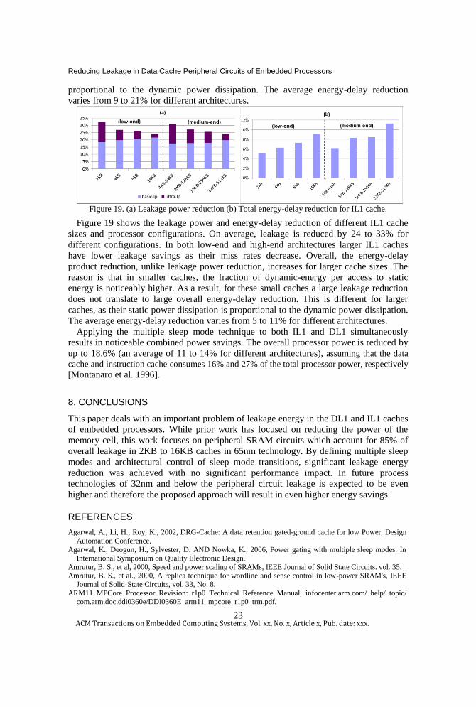
Figure 19 shows the leakage power and energy-delay reduction of different IL1 cache
sizes and processor configurations. On average, leakage is reduced by 24 to 33% for
different configurations. In both low-end and high-end architectures larger IL1 caches
have lower leakage savings as their miss rates decrease. Overall, the energy-delay
product reduction, unlike leakage power reduction, increases for larger cache sizes. The
reason is that in smaller caches, the fraction of dynamic-energy per access to static
energy is noticeably higher. As a result, for these small caches a large leakage reduction
does not translate to large overall energy-delay reduction. This is different for larger
caches, as their static power dissipation is proportional to the dynamic power dissipation.
The average energy-delay reduction varies from 5 to 11% for different architectures.
Applying the multiple sleep mode technique to both IL1 and DL1 simultaneously
results in noticeable combined power savings. The overall processor power is reduced by
up to 18.6% (an average of 11 to 14% for different architectures), assuming that the data
cache and instruction cache consumes 16% and 27% of the total processor power, respectively
[Montanaro et al. 1996].
8. CONCLUSIONS
This paper deals with an important problem of leakage energy in the DL1 and IL1 caches
of embedded processors. While prior work has focused on reducing the power of the
memory cell, this work focuses on peripheral SRAM circuits which account for 85% of
overall leakage in 2KB to 16KB caches in 65nm technology. By defining multiple sleep
modes and architectural control of sleep mode transitions, significant leakage energy
reduction was achieved with no significant performance impact. In future process
technologies of 32nm and below the peripheral circuit leakage is expected to be even
higher and therefore the proposed approach will result in even higher energy savings.
REFERENCES
Agarwal, A., Li, H., Roy, K., 2002, DRG-Cache: A data retention gated-ground cache for low Power, Design
Automation Conference. Agarwal, K., Deogun, H., Sylvester, D. AND Nowka, K., 2006, Power gating with multiple sleep modes. In
International Symposium on Quality Electronic Design.
Amrutur, B. S., et al, 2000, Speed and power scaling of SRAMs, IEEE Journal of Solid State Circuits. vol. 35. Amrutur, B. S., et al., 2000, A replica technique for wordline and sense control in low-power SRAM's, IEEE
Journal of Solid-State Circuits, vol. 33, No. 8.
ARM11 MPCore Processor Revision: r1p0 Technical Reference Manual, infocenter.arm.com/ help/ topic/ com.arm.doc.ddi0360e/DDI0360E_arm11_mpcore_r1p0_trm.pdf.
● H. Homayoun, A. Veidenbaum, A. Sasan and Dean M. Tullsen
ACM Transactions on Embedded Computing Systems, Vol. xx, No. x, Article x, Pub. date: xxx.
24
Calhoun, B. H. Honore, F A., AND Chandrakasan, A., 2003, Design methodology for fine-grained leakage
control in MTCMOS,” in Int. Symp. Low Power Electronics and Design, pp.104-109.
Chun, S., AND Skadron, K., 2008, On-Demand Solution to Minimize I-Cache Leakage Energy with Maintaining Performance”, IEEE Transactions on Computers.
Design Compiler, Synopsys Incorporation.
Flautner, K., et al, 2002, Drowsy caches: simple techniques for reducing leakage power. IEEE ISCA. Gerosa, G., Curtis, S.D., Addeo, M., Jiang B., Kuttanna, B., Merchant, F., Patel, B., Taufique, M. AND
Samarchi, H., 2008, A Sub-lW to 2W Low-Power IA Processor for Mobile Internet Devices and Ultra-
Mobile PCs in 45nm Hi-K Metal Gate CMOS, in International Solid State Circuits Conference. Grossara, E., et al., 2006, Statistically Aware SRAM Memory Array Design, in International Symposium on
Quality Electronic Design, ISQED.
Homayoun, H., Makhzan M., AND Veidenbaum, A., 2008, Multiple Sleep Mode Leakage Control for Cache Peripheral Circuits in Embedded Processors, In Proceedings of the 2008 International Conference on
Compilers, Architecture, and Synthesis for Embedded Systems, CASES, Atlanta, U.S.A.
Homayoun, H., Makhzan, M., and Veidenbaum, A., 2008, ZZ-HVS: Zig-zag horizontal and vertical sleep transistor sharing to reduce leakage power in on chip SRAM peripheral circuits, in Proc. IEEE International
Conference on Computer Design, pp.699–706.
Horiguchi, M., Sakata, T., AND Itoh, K., 1993, Switched-source-impedence CMOS circuit for low-standby subthreshold current giga-scale LSI’s, IEEE Journal of Solid-State Circuits.
Kao, J., Narendra, S., AND Chandrakasan, A., 1998, MTCMOS hierarchical sizing based on mutual exclusive
discharge patterns, Design Automation Conference. Kaxiras, S., et al, 2001, Cache decay: exploiting generational behavior to reduce cache leakage power. IEEE-
ISCA.
Khandelwal, V., AND Srivastava, A., 2004, Leakage control through fine-grained placement and sizing of sleep transistors, in Proc. ACM/IEEE Int. Conf. on Computer Aided Design, pp. 533-536.
Kim, C. H., et al,. 2005, A forward body-biased low-leakage SRAM cache: device, circuit and architecture considerations. IEEE Trans. on VLSI Systems, vol. 13.
Kim, S. H. , AND Mooney, V. J., 2006, Sleepy keeper: a new approach to low-leakage power VLSI design,
VLSI-SoC.
Ku, J. C. , Ozdemir, S., Memik, G., AND Ismail, Y., 2006, Power Density Minimization for Highly-
Associative Caches in Embedded Processors, GLSVLSI.
Mai, K. W., Mori, T., Amrutur, B. S., Ho, R., Wilburn, B., Horowitz, M. A. , Fukushi, I., Izawa, T., AND Mitarai, S., 1998, Low-Power SRAM Design Using Half-Swing Pulse-Mode Techniques, IEEE Journal of
Solid-State Circuits, vol. 33, no. 11, pp.1659-1671.
Mamidipaka, M., Khouri, K.S., Dutt, N., AND Abadir, M. S., 2004, Analytical models for leakage power estimation of memory array structures. CODES+ISSS.
Margala, M., 1999, Low power SRAM circuit design, In IEEE International Workshop on Memory
Technology, Design, and Testing, 115–122. Meng, Y., Sherwood, T., AND Kastner, R., 2005, On the limits of leakage power reduction in caches. In
International Symposium on High-Performance Computer Architecture.
MiBench Version 1.0. http://www.eecs.umich.edu/mibench/. Min, K.-S., Kawaguchi, H. AND Sakurai, T., 2003, Zigzag super cut-off CMOS (ZSCCMOS) block activation
with self-adaptive voltage level controller: an alternative to clock-gating scheme in leakage dominant era,
IEEE International Solid State Circuits Conference. Montanaro, J., Witek, R. T., Anne, K., Black, A. J., Cooper, E. M., Dobberpuhl, D. W., Donohue, P. M., Eno,
J., Hoeppner, W., Kruckemyer, D., Lee, T. H., Lin, P. C. M., Madden, L., Murray, D., Pearce, M. H.,
Santhanam, S., Snyder, K. J., Stephany, R., AND Thierauf, S.C., 1996, A 160-MHz, 32-b, 0.5-W CMOS RISC microprocessor, IEEE J. Solid-State Circuits, vol. 31, pp. 1703–1714.
Mutoh, S., Shigematsu, S., Gotoh, Y., AND Konaka, S., 1999, Design method of MTCMOS power switch for
lowvoltage high-speed LSIs,” in Proc. Asian and South Pacific Design Automation Conf, pp. 113-116. Nakagome Y., et al., 2003, Review and future prospects of low-voltage RAM circuits, IBM Journal of R&D.
Nicolaescu, D., Salamat, B., Veidenbaum, A. AND Valero, M., 2006, Fast Speculative Address Generation and
Way Caching for Reducing L1 Data Cache Energy. Proc. IEEE International Conference on Computer Design.
Nii, K et al. 2004, A 90-nm low-power 32-kB embedded SRAM with gate leakage suppression circuit for
mobile applications. IEEE Journal of Solid-state Circuits, Vol. 39, No. 4: 684-693. Nii, K., et al. 1998, A low power SRAM using auto-backgate-controlled MT-CMOS. In International
Symposium on Low-Power Electronics, pp. 293-298.
Park, J. C. AND Mooney III, V. J., 2006, Sleepy stack leakage reduction. IEEE Trans. VLSI Syst. 14(11): 1250-1263.

Reducing Leakage in Data Cache Peripheral Circuits of Embedded Processors
ACM Transactions on Embedded Computing Systems, Vol. xx, No. x, Article x, Pub. date: xxx.
25
Powell M., et al,. 2000 Gated-Vdd: A Circuit Technique to Reduce Leakage in Deep-Submicron Cache
Memories. IEEE-ISLPED.
Rabaey, J. M., Chandrakasan, A. P. AND Nikolić, B., 2003, Digital integrated circuits: a design perspective, Prentice Hall, Second. Edition.
Ramalingam, A., Zhang, B., Davgan, A., AND Pan, D., 2005, “Sleep Transistor Sizing Using Timing
Criticality and Temporal Currents,” Proc. ASP-DAC. Rusu, S., et al, 2007, A 65-nm Dual-Core Multithreaded Xeon® Processor With 16-MB L3 Cache, IEEE
Journal Of Solid-State Circuits, VOL. 42.
SimpleScalar4 tutorial, http://www.simplescalar.com/tutorial.html. Semiconductor Industries Association, 2005, International Technology Roadmap for Semiconductors,
http://www.itrs.net/.
Takeyama, Y. Otake, H., Hirabayashi, O., AND Kushida, K. N, 2006, A Low Leakage SRAM Macro with Replica Cell Biasing Scheme. IEEE Journ al Of Solid- State Circuits, Vol. 41, No. 4.
Thoziyoor, S., Muralimanohar, N., Ahn, J.H., AND Jouppi, N.P., 2008, CACTI 5.1 Technical Report, HP
Laboratories, Palo Alto. Zhang, W., AND Hu, J. S., 2002, Compiler-directed instruction cache leakage optimization. In Proc. In
International Symposium on Microarchitecture.


![TruSpy: Cache Side-Channel Information Leakage … › 2016 › 980.pdfrecent ARM processors support this security extension [25], [26]. The traditional operating domain is called](https://img.pdfslide.net/doc/110x75/5f0fbc1c7e708231d4459fe3/truspy-cache-side-channel-information-leakage-a-2016-a-980pdf-recent-arm-processors.jpg)
![CS4HS Jihong Kim 2012 Proceeding용 최종본 · 2018-08-17 · Leakage Management by Turning Off Replications [Kim2009] Replicating the shared block in each private L2 cache Th h](https://img.pdfslide.net/doc/110x75/5e6c401f56e66106584bda9e/cs4hs-jihong-kim-2012-proceeding-oee-2018-08-17-leakage-management-by.jpg)