Embed Size (px)
Citation preview
Reduction of Secondary Electron Yield for E-cloud Mitigation by
Laser Ablation Surface Engineering
R. Valizadeh1, O.B. Malyshev1, S. Wang1,2, T. Sian1,3, M. D. Cropper2 and N. Sykes4
1 ASTeC, STFC Daresbury Laboratory, Warrington WA4 4AD, UK
2 Department of Physics, Loughborough University, Loughborough LE11 3TU, UK 3 The Photon Science Institute, The University of Manchester, Manchester M13 9PL, UK
4 Micronanics Ltd., Didcot, Oxon OX11 0QX, UK
Abstract Developing a surface with low Secondary Electron Yield (SEY) is one of the main ways of mitigating
electron cloud and beam-induced electron multipacting in high-energy charged particle accelerators. In
our previous publications, a low SEY< 0.9 for as-received metal surfaces modified by a nanosecond
pulsed laser was reported. In this paper, the SEY of laser-treated blackened copper has been investigated
as a function of different laser irradiation parameters. We explore and study the influence of micro- and
nano-structures induced by laser surface treatment in air of copper samples as a function of various laser
irradiation parameters such as peak power, laser wavelength ( = 355 nm and 1064 nm), number of pulses
per point (scan speed and repetition rate) and fluence, on the SEY. The surface chemical composition was
determined by x-ray photoelectron spectroscopy (XPS) which revealed that heating resulted in diffusion
of oxygen into the bulk and induced the transformation of CuO to sub-stoichiometric oxide. The surface
topography was examined with high resolution scanning electron microscopy (HRSEM) which showed
that the laser-treated surfaces are dominated by microstructure grooves and nanostructure features.
1. INTRODUCTION
In high intensity particle accelerators with positively charged beams such as the LHC [1,2,3], KEKB [4],
DAFNE [5], RHIC [6], PEP=II [7], etc., the beam induced electron multipacting (BIEM) and electron cloud
(e-cloud) effects can significantly affect the quality of the beam and machine operation [8,9]. E-cloud was
first observed on the proton/antiproton collider VAPP in the Budker Institute of Nuclear Physics in 1965
[10,11]. After more than 50 years since the first observation, the e-cloud remains a potential problem for
many high intensity machines, thus the e-cloud has been studied for ILC [12] and is being investigated for
the HL-LHC [13] and the FCC [14]. The initial electrons may appear due to synchrotron radiation producing
photoelectrons or beam induced residual gas ionisation. These electrons can be accelerated up to several
hundreds of eV in the electric field of the passing bunch. On colliding with the chamber wall, they will in
turn produce further secondary electrons. This amplification leads to the build-up and dissipation of an
electron cloud (e-cloud) along the beam path. E-cloud can affect the operation and performance of high
energy charged particle accelerators in a variety of ways. It can induce increases in emittance, beam
instability, vacuum pressure, beam losses, reduction in the beam lifetime, or additional heat loads on a
(cryogenic) vacuum chamber. In RF wave guides, electron multipacting limits their lifetime and causes
power loss, whereas in detectors the secondary electrons define the signal background and reduce the
sensitivity.
It has been shown both theoretically and experimentally [3] that the e-cloud density build-up depends on
the SEY function (E) and to minimize the effects of e-cloud, the max value should be less than a certain
threshold value, but in most cases max < 1 would be a sufficient condition [3,15].
Since the secondary electron yield is influenced by the wall material, surface chemistry, topography and
electron energy, any deliberate mitigation mechanism is based on engineering the first three of these
parameters. There are a few ways of reducing the SEY:
(a) Choice of material with low SEY (for example, Cu has lower SEY than Al);
(b) Modifying surface geometry (e.g. making grooves) [3,16];
(c) Coating with low SEY materials (such as TiN [17], NEG [18] and amorphous carbon (a-C) [19]);
(d) Coating with low SEY microstructure (ex.: copper black, gold black; columnar NEG) [20,21,22];
(f) Various combinations of above.
Recently, a low SEY< 0.9 for as-received metal surfaces modified by a nanosecond pulsed laser was
reported for the first time by Valizadeh et.al. [23,24]. Further development of this surfaces led to even lower
value of SEY <0.6 [25]. In comparison with other technologies for currently used surface engineering the
laser treatment has a few advantages:
The equipment is simpler;
There is no need for vacuum or clean room facilities;
Hierarchical structures containing both micro- and nanostructures can be created in a single laser
treatment process; thus, the process is efficient;
Surface modification is performed through a beam of light and thus contactless.
This work was focused on studying the influence of micro- and nano-structures induced by laser surface
treatment in air of copper samples as function of various laser irradiation parameters such as peak power,
laser, number of pulses per point (scan speed and repetition rate) and fluence, on the SEY.
2. EXPERIMENTAL
2.1 Sample preparation
2.1.1. Laser treated samples
The samples were made of commercially available rolled, electro-polished oxygen-free copper (Cu) with
high purity of 99.999% and thickness of 1 mm, 50 and 100 μm. Prior to laser exposure the samples were
degreased. The samples were washed with acetone and then were irradiated by pulses of a Nd:YAG laser
with different pulse durations operated at basic IR and third harmonic UV wavelength (1064 and 355 nm)
and various repetition rates ranging from 2.5 to 100 kHz. In all cases the laser beam had a Gaussian intensity
profile and was focused on to the substrate surface using a flat-field scanning lens system. The diameter of
the focused laser spot on each substrate between the points where the intensity has fallen to 1/e2 of the
central value was set at 25 m for = 1064 nm and 15 m for = 355 nm. The laser beam spot was scanned
by galvanometric scanner across a 15 mm 15 mm sized area of the substrate. The pulse number reaching a
given spot area was determined by varying the scanning speed, pulse repetition and the beam diameter. The
laser fluence was varied between 2 and 154 J/cm2. All the samples were irradiated in air at atmospheric
pressure and at room temperature. Six sets of different laser parameters were used for this study shown in
Table 1. The samples used in this study are summarised in Table 2.
Table 1: Different laser treatment parameters used for surface treatment.
Laser
treatment
condition
(nm) Average
power
(W)
Spot
size
( m)
Pulse
duration
(ns)
Pulse
repetition
(kHz)
Pitch
width
( m)
Scan
speed
(mm/s)
Energy
per
pulse
( J)
Fluence
(J/cm2)
1 355 3 15 25 40 10 30,60,90,
120, 180
75 42
2 1064 1.9 25 70 2.5 20 125 760 154
3 1064 2.4 25 70 5.0 20 125 480 97
4 1064 3.6 25 70 10 20 30 360 73
5 1064 3 25 70 20 10 500 150 30
6 1064 1 25 70 100 10 500 10 2
Table 2. List of samples.
Sample no. Thickness Description Condition Parameters
1 1 mm Cu reference sample No treatment -
2 1 mm First laser system (λ
= 355 nm)
Condition 1, scan
speed varying
180 mm/s
3 1 mm 120 mm/s
4 1 mm 90 mm/s
5 1 mm 60 mm/s
6 1 mm 30 mm/s
7 100 μm Second laser system
(λ = 1064 nm)
Condition 2 2.5 kHz
8 100 μm Condition 3 5.0 kHz
9 100 μm Condition 4 10 kHz
2* 1 mm Second laser
treatments
Condition 5 and 6 500 mm/s
3* 1 mm Condition 5 and 6 500 mm/s
10 0.5 mm Cu powder No treatment
-
11 <10 μm -
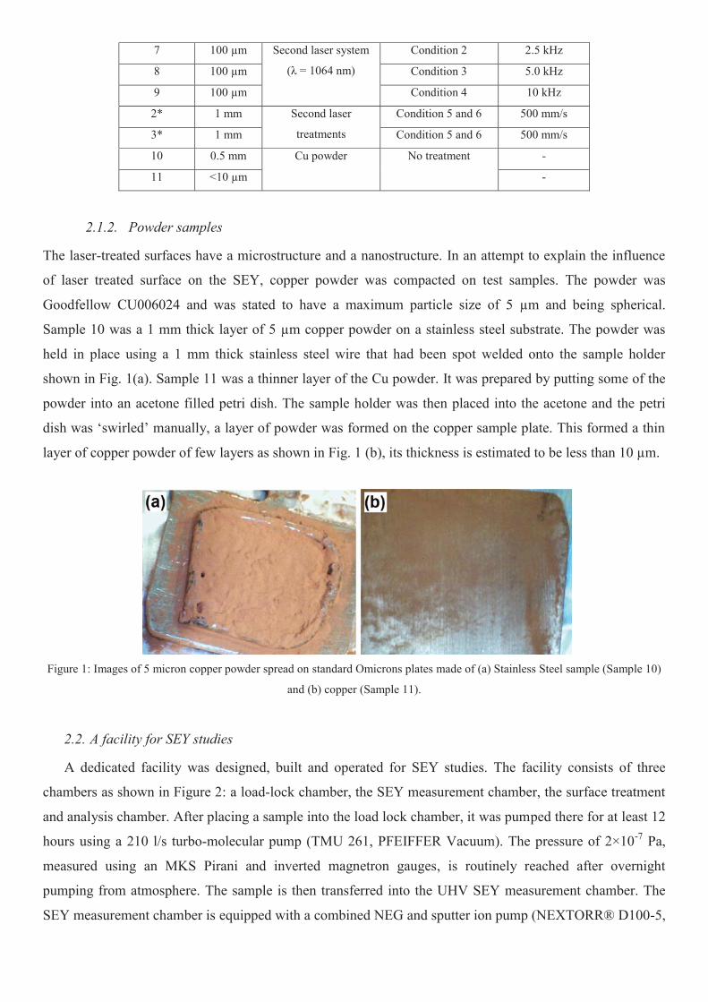
2.1.2. Powder samples
The laser-treated surfaces have a microstructure and a nanostructure. In an attempt to explain the influence
of laser treated surface on the SEY, copper powder was compacted on test samples. The powder was
Goodfellow CU006024 and was stated to have a maximum particle size of 5 μm and being spherical.
Sample 10 was a 1 mm thick layer of 5 μm copper powder on a stainless steel substrate. The powder was
held in place using a 1 mm thick stainless steel wire that had been spot welded onto the sample holder
shown in Fig. 1(a). Sample 11 was a thinner layer of the Cu powder. It was prepared by putting some of the
powder into an acetone filled petri dish. The sample holder was then placed into the acetone and the petri
dish was ‘swirled’ manually, a layer of powder was formed on the copper sample plate. This formed a thin
layer of copper powder of few layers as shown in Fig. 1 (b), its thickness is estimated to be less than 10 μm.
Figure 1: Images of 5 micron copper powder spread on standard Omicrons plates made of (a) Stainless Steel sample (Sample 10)
and (b) copper (Sample 11).
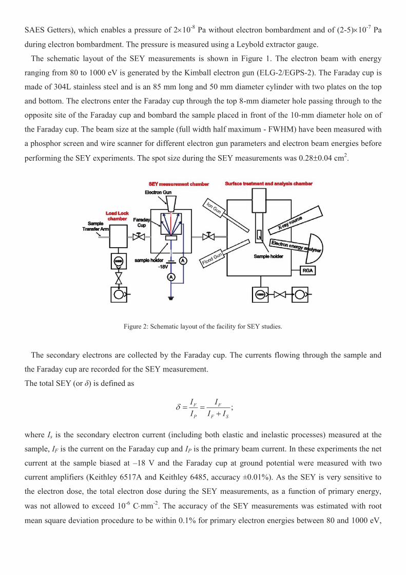
2.2. A facility for SEY studies
A dedicated facility was designed, built and operated for SEY studies. The facility consists of three
chambers as shown in Figure 2: a load-lock chamber, the SEY measurement chamber, the surface treatment
and analysis chamber. After placing a sample into the load lock chamber, it was pumped there for at least 12
hours using a 210 l/s turbo-molecular pump (TMU 261, PFEIFFER Vacuum). The pressure of 2×10⁻⁷ Pa,
measured using an MKS Pirani and inverted magnetron gauges, is routinely reached after overnight
pumping from atmosphere. The sample is then transferred into the UHV SEY measurement chamber. The
SEY measurement chamber is equipped with a combined NEG and sputter ion pump (NEXTORR® D100-5,
SAES Getters), which enables a pressure of 2 10-8 Pa without electron bombardment and of (2-5) 10-7 Pa
during electron bombardment. The pressure is measured using a Leybold extractor gauge.
The schematic layout of the SEY measurements is shown in Figure 1. The electron beam with energy
ranging from 80 to 1000 eV is generated by the Kimball electron gun (ELG-2/EGPS-2). The Faraday cup is
made of 304L stainless steel and is an 85 mm long and 50 mm diameter cylinder with two plates on the top
and bottom. The electrons enter the Faraday cup through the top 8-mm diameter hole passing through to the
opposite site of the Faraday cup and bombard the sample placed in front of the 10-mm diameter hole on of
the Faraday cup. The beam size at the sample (full width half maximum - FWHM) have been measured with
a phosphor screen and wire scanner for different electron gun parameters and electron beam energies before
performing the SEY experiments. The spot size during the SEY measurements was 0.28 0.04 cm2.
Figure 2: Schematic layout of the facility for SEY studies.
The secondary electrons are collected by the Faraday cup. The currents flowing through the sample and
the Faraday cup are recorded for the SEY measurement.
The total SEY (or δ) is defined as
;F F
P F S
I II I I
where Is is the secondary electron current (including both elastic and inelastic processes) measured at the
sample, IF is the current on the Faraday cup and IP is the primary beam current. In these experiments the net
current at the sample biased at –18 V and the Faraday cup at ground potential were measured with two
current amplifiers (Keithley 6517A and Keithley 6485, accuracy ±0.01%). As the SEY is very sensitive to
the electron dose, the total electron dose during the SEY measurements, as a function of primary energy,
was not allowed to exceed 10-6 C mm-2. The accuracy of the SEY measurements was estimated with root
mean square deviation procedure to be within 0.1% for primary electron energies between 80 and 1000 eV,
however the repeatability of SEY for the same sample over different area of the sample lies within ±2.5%
which could be explained by small non-uniformity of the surface topography of studied samples.
After SEY measurements the sample can be transferred to the surface treatment and analysis chamber
which is equipped with a flood gun (AG 31F, VG) used for electron conditioning (electron energy 485 eV
and the accuracy of the electron dose was within 10%), an argon ion gun (PSP, ISIS 3000) with energy of
1.5 keV for surface etching and a sample heater which allows sample heating up to 300 C. In addition the
sample surface composition and chemical bonding energies can be analysed using an X-ray source and an
electron energy analyser. XPS measurements are carried out using a hemispherical analyser fitted with a
five channeltron detector. Power supplies are for the spectrometer a PSP Resolve Control and, for the
detectors, a PSP #705. The spectrometer was operated at 20 eV pass energy at all times and the angle
between the X-ray source and electron analyser is 70 degree. Photo-electrons are excited by non-
monochromatic Al Kα X-ray source (hv = 1463 eV) using VG twin anode, the Al anode used at all times
operated at 10 keV, 20 mA.
The surface treatment and analysis chamber is equipped with a 340 l/s turbo-molecular pump (Leybold
340M) and 1000 l/s getter pump (CapaciTorr® D-1000 Pump, SAES Getters). The base pressure of about
10-7 Pa measured by a Leybold extractor gauge and the residual gas composition was monitored using a
residual gas analyser (RGA, VG Thermo, VGQ).
The typical experimental procedure may involve SEY measurement of the as-received sample followed
by XPS measurement, conditioning using the diffuse-beamed electrons from the flood gun, ion
bombardment or thermal treatment, followed by another XPS measurement and another SEY measurement,
etc.
3. RESULTS:
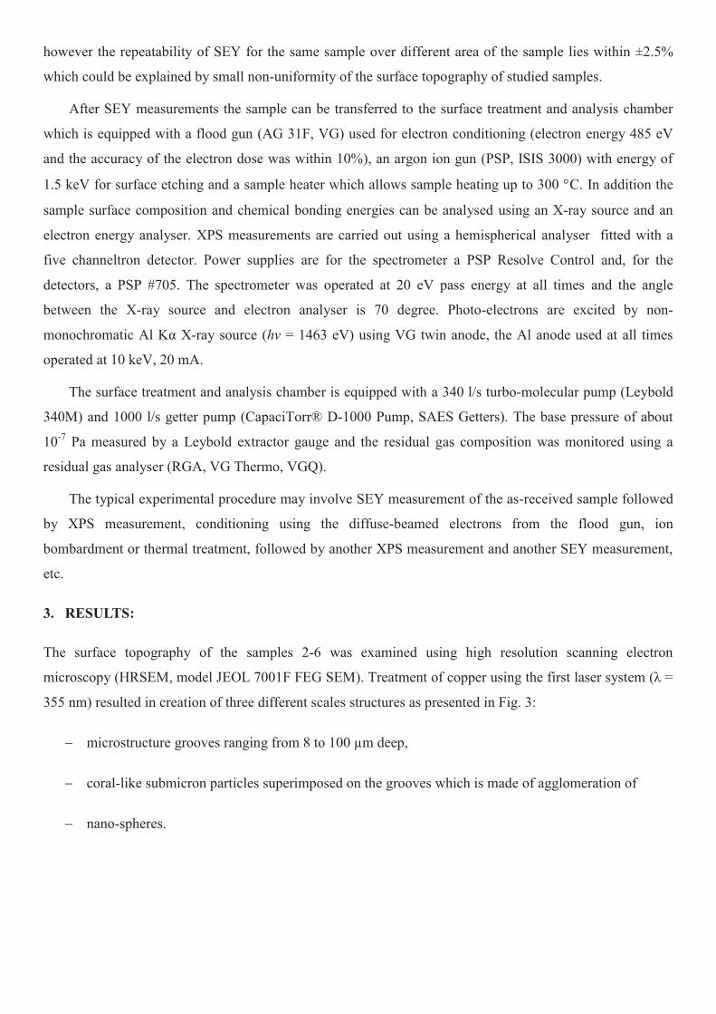
The surface topography of the samples 2-6 was examined using high resolution scanning electron
microscopy (HRSEM, model JEOL 7001F FEG SEM). Treatment of copper using the first laser system (λ =
355 nm) resulted in creation of three different scales structures as presented in Fig. 3:
microstructure grooves ranging from 8 to 100 μm deep,
coral-like submicron particles superimposed on the grooves which is made of agglomeration of
nano-spheres.
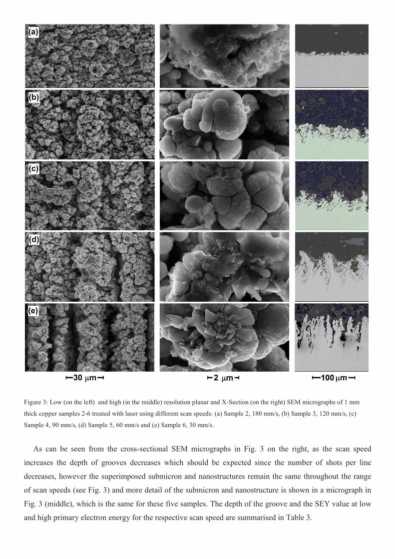
Figure 3: Low (on the left) and high (in the middle) resolution planar and X-Section (on the right) SEM micrographs of 1 mm
thick copper samples 2-6 treated with laser using different scan speeds: (a) Sample 2, 180 mm/s, (b) Sample 3, 120 mm/s, (c)
Sample 4, 90 mm/s, (d) Sample 5, 60 mm/s and (e) Sample 6, 30 mm/s.
As can be seen from the cross-sectional SEM micrographs in Fig. 3 on the right, as the scan speed
increases the depth of grooves decreases which should be expected since the number of shots per line
decreases, however the superimposed submicron and nanostructures remain the same throughout the range
of scan speeds (see Fig. 3) and more detail of the submicron and nanostructure is shown in a micrograph in
Fig. 3 (middle), which is the same for these five samples. The depth of the groove and the SEY value at low
and high primary electron energy for the respective scan speed are summarised in Table 3.
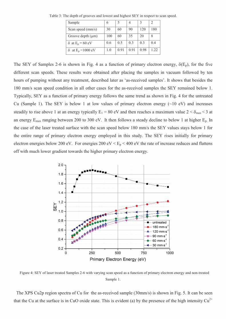
Table 3: The depth of grooves and lowest and highest SEY in respect to scan speed.
Sample 6 5 4 3 2
Scan speed (mm/s) 30 60 90 120 180
Groove depth (μm) 100 60 35 20 8
at Ep = 60 eV 0.6 0.5 0.3 0.3 0.4
at Ep =1000 eV 1.0 0.91 0.91 0.98 1.22
The SEY of Samples 2-6 is shown in Fig. 4 as a function of primary electron energy, (Ep), for the five
different scan speeds. These results were obtained after placing the samples in vacuum followed by ten
hours of pumping without any treatment, described later as ‘as-received samples’. It shows that besides the
180 mm/s scan speed condition in all other cases for the as-received samples the SEY remained below 1.
Typically, SEY as a function of primary energy follows the same trend as shown in Fig. 4 for the untreated
Cu (Sample 1). The SEY is below 1 at low values of primary electron energy (~10 eV) and increases
steadily to rise above 1 at an energy typically E1 = 80 eV and then reaches a maximum value 2 < max < 3 at
an energy Emax ranging between 200 to 300 eV. It then follows a steady decline to below 1 at higher Ep. In
the case of the laser treated surface with the scan speed below 180 mm/s the SEY values stays below 1 for
the entire range of primary electron energy employed in this study. The SEY rises initially for primary
electron energies below 200 eV. For energies 200 eV < Ep < 400 eV the rate of increase reduces and flattens
off with much lower gradient towards the higher primary electron energy.
Figure 4: SEY of laser treated Samples 2-6 with varying scan speed as a function of primary electron energy and non-treated
Sample 1.
The XPS Cu2p region spectra of Cu for the as-received sample (30mm/s) is shown in Fig. 5. It can be seen
that the Cu at the surface is in CuO oxide state. This is evident (a) by the presence of the high intensity Cu2+
broad peak shake up satellites at about 9 eV higher binding energy than the main 2p3/2 and 2p1/2 peaks at
binding energy of 943 and 963 eV and (b) from the distinctive x-ray exited Cu LMM Auger spectra at 917
eV kinetic energy shown as inset in Fig. 5. Also, in all cases no carbon peak was observed.
Figure 5: XPS spectra of Cu2p region for the scan speed of 30mm/s used with 355 nm laser. The inset is the X-ray exited Cu
LMM Auger.
Figures 6 and 7 represent the planar view of copper surfaces of Samples 7 and 8 being treated with laser
parameters 2 and 3 as stated in Table 1. Where Fig. 6 shows the low resolution image which is similar for
both conditions and Fig. 7 shows the difference between them at higher resolution. In both cases the surface
consists of a shallow microgrooves, sub-microstructures resembling volcanic sponges covered with nano-
size wire/filament/fibre like structure.
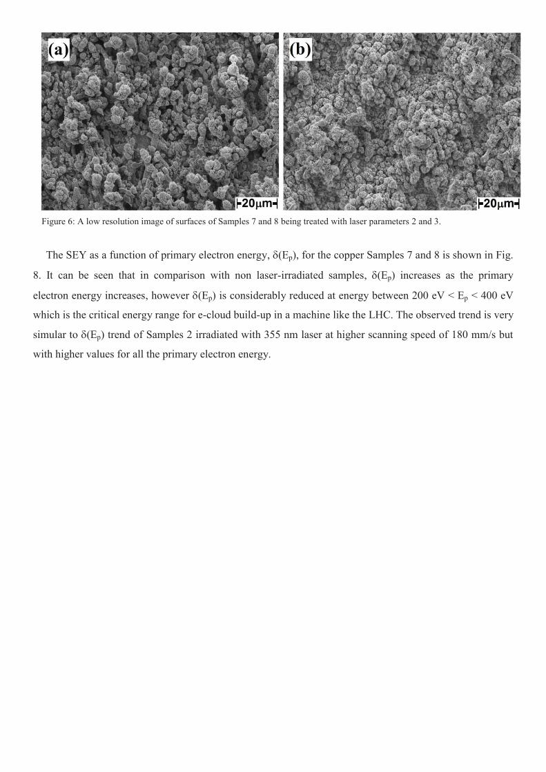
Figure 6: A low resolution image of surfaces of Samples 7 and 8 being treated with laser parameters 2 and 3.
The SEY as a function of primary electron energy, (Ep), for the copper Samples 7 and 8 is shown in Fig.
8. It can be seen that in comparison with non laser-irradiated samples, (Ep) increases as the primary
electron energy increases, however (Ep) is considerably reduced at energy between 200 eV < Ep < 400 eV
which is the critical energy range for e-cloud build-up in a machine like the LHC. The observed trend is very
simular to (Ep) trend of Samples 2 irradiated with 355 nm laser at higher scanning speed of 180 mm/s but
with higher values for all the primary electron energy.
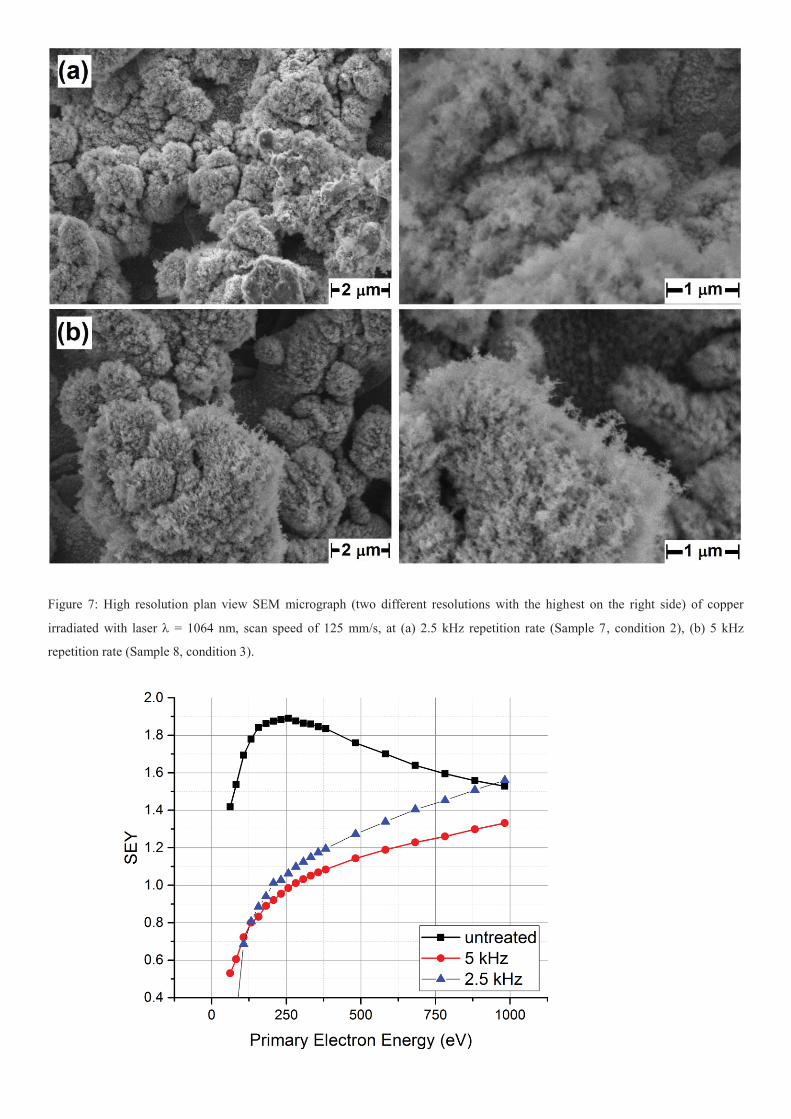
Figure 7: High resolution plan view SEM micrograph (two different resolutions with the highest on the right side) of copper
irradiated with laser = 1064 nm, scan speed of 125 mm/s, at (a) 2.5 kHz repetition rate (Sample 7, condition 2), (b) 5 kHz
repetition rate (Sample 8, condition 3).
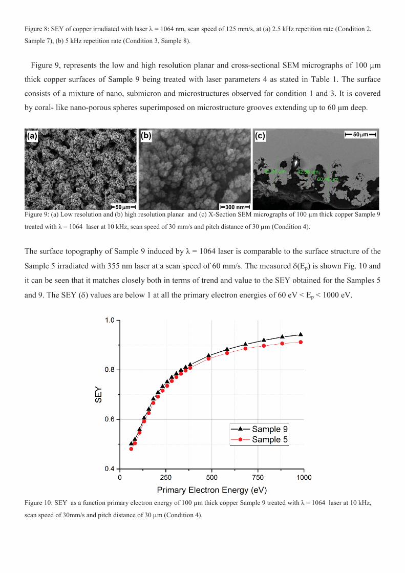
Figure 8: SEY of copper irradiated with laser = 1064 nm, scan speed of 125 mm/s, at (a) 2.5 kHz repetition rate (Condition 2,
Sample 7), (b) 5 kHz repetition rate (Condition 3, Sample 8).
Figure 9, represents the low and high resolution planar and cross-sectional SEM micrographs of 100 μm
thick copper surfaces of Sample 9 being treated with laser parameters 4 as stated in Table 1. The surface
consists of a mixture of nano, submicron and microstructures observed for condition 1 and 3. It is covered
by coral- like nano-porous spheres superimposed on microstructure grooves extending up to 60 μm deep.
Figure 9: (a) Low resolution and (b) high resolution planar and (c) X-Section SEM micrographs of 100 μm thick copper Sample 9
treated with λ = 1064 laser at 10 kHz, scan speed of 30 mm/s and pitch distance of 30 m (Condition 4).
The surface topography of Sample 9 induced by λ = 1064 laser is comparable to the surface structure of the
Sample 5 irradiated with 355 nm laser at a scan speed of 60 mm/s. The measured (Ep) is shown Fig. 10 and
it can be seen that it matches closely both in terms of trend and value to the SEY obtained for the Samples 5
and 9. The SEY ( ) values are below 1 at all the primary electron energies of 60 eV < Ep < 1000 eV.
Figure 10: SEY as a function primary electron energy of 100 μm thick copper Sample 9 treated with λ = 1064 laser at 10 kHz,
scan speed of 30mm/s and pitch distance of 30 m (Condition 4).
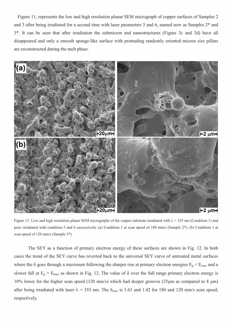
Figure 11, represents the low and high resolution planar SEM micrograph of copper surfaces of Samples 2
and 3 after being irradiated for a second time with laser parameters 5 and 6, named now as Samples 2* and
3*. It can be seen that after irradiation the submicron and nanostructures (Figure 3c and 3d) have all
disappeared and only a smooth sponge-like surface with protruding randomly oriented micron size pillars
are reconstructed during the melt phase.
Figure 11: Low and high resolution planar SEM micrographs of the copper substrate irradiated with = 355 nm (Condition 1) and
post- irradiated with condition 5 and 6 successively. (a) Condition 1 at scan speed of 180 mm/s (Sample 2*), (b) Condition 1 at
scan speed of 120 mm/s (Sample 3*).
The SEY as a function of primary electron energy of these surfaces are shown in Fig. 12. In both
cases the trend of the SEY curve has reverted back to the universal SEY curve of untreated metal surfaces
where the goes through a maximum following the sharper rise at primary electron energies Ep < Emax and a
slower fall at Ep > Emax as shown in Fig. 12. The value of over the full range primary electron energy is
10% lower for the higher scan speed (120 mm/s) which had deeper grooves (25μm as compared to 8 μm)
after being irradiated with laser = 355 nm. The max is 1.63 and 1.42 for 180 and 120 mm/s scan speed,
respectively.
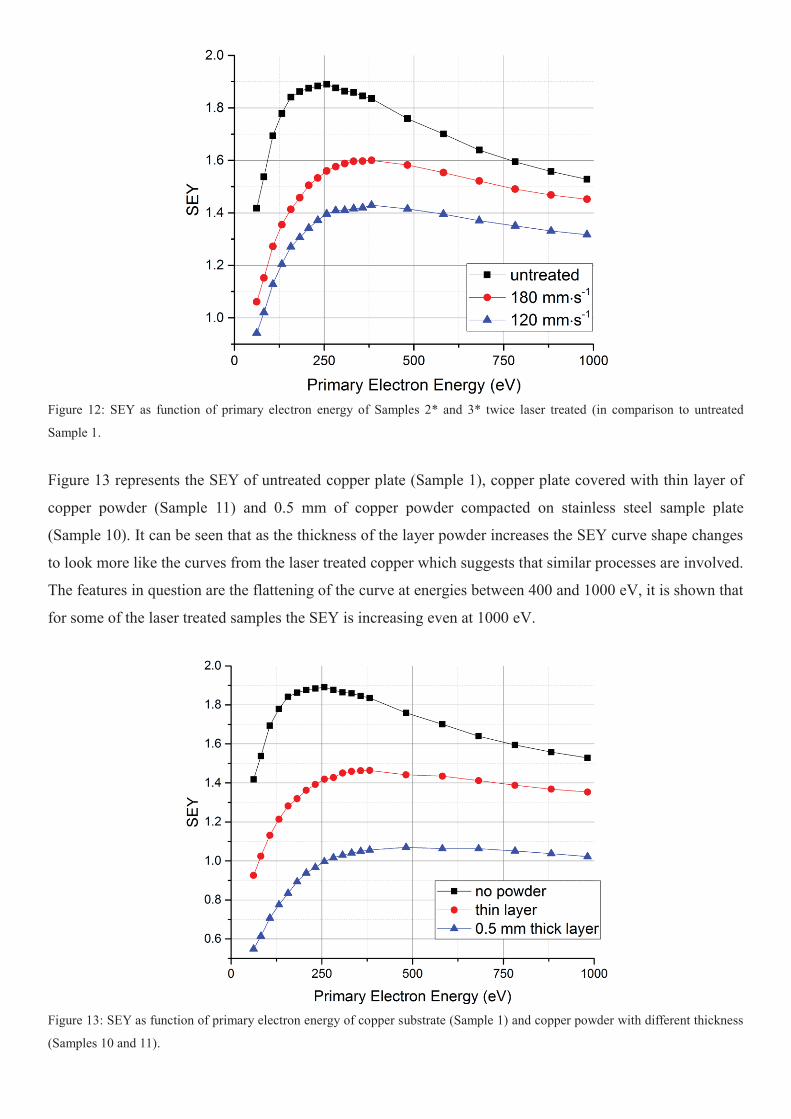
Figure 12: SEY as function of primary electron energy of Samples 2* and 3* twice laser treated (in comparison to untreated
Sample 1.
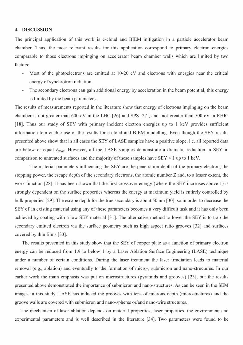
Figure 13 represents the SEY of untreated copper plate (Sample 1), copper plate covered with thin layer of
copper powder (Sample 11) and 0.5 mm of copper powder compacted on stainless steel sample plate
(Sample 10). It can be seen that as the thickness of the layer powder increases the SEY curve shape changes
to look more like the curves from the laser treated copper which suggests that similar processes are involved.
The features in question are the flattening of the curve at energies between 400 and 1000 eV, it is shown that
for some of the laser treated samples the SEY is increasing even at 1000 eV.
Figure 13: SEY as function of primary electron energy of copper substrate (Sample 1) and copper powder with different thickness
(Samples 10 and 11).
4. DISCUSSION
The principal application of this work is e-cloud and BIEM mitigation in a particle accelerator beam
chamber. Thus, the most relevant results for this application correspond to primary electron energies
comparable to those electrons impinging on accelerator beam chamber walls which are limited by two
factors:
- Most of the photoelectrons are emitted at 10-20 eV and electrons with energies near the critical
energy of synchrotron radiation.
- The secondary electrons can gain additional energy by acceleration in the beam potential, this energy
is limited by the beam parameters.
The results of measurements reported in the literature show that energy of electrons impinging on the beam
chamber is not greater than 600 eV in the LHC [26] and SPS [27], and not greater than 500 eV in RHIC
[18]. Thus our study of SEY with primary incident electron energies up to 1 keV provides sufficient
information tom enable use of the results for e-cloud and BIEM modelling. Even though the SEY results
presented above show that in all cases the SEY of LASE samples have a positive slope, i.e. all reported data
are below or equal Emax. However, all the LASE samples demonstrate a dramatic reduction in SEY in
comparison to untreated surfaces and the majority of these samples have SEY < 1 up to 1 keV.
The material parameters influencing the SEY are the penetration depth of the primary electron, the
stopping power, the escape depth of the secondary electrons, the atomic number Z and, to a lesser extent, the
work function [28]. It has been shown that the first crossover energy (where the SEY increases above 1) is
strongly dependent on the surface properties whereas the energy at maximum yield is entirely controlled by
bulk properties [29]. The escape depth for the true secondary is about 50 nm [30], so in order to decrease the
SEY of an existing material using any of these parameters becomes a very difficult task and it has only been
achieved by coating with a low SEY material [31]. The alternative method to lower the SEY is to trap the
secondary emitted electron via the surface geometry such as high aspect ratio grooves [32] and surfaces
covered by thin films [33].
The results presented in this study show that the SEY of copper plate as a function of primary electron
energy can be reduced from 1.9 to below 1 by a Laser Ablation Surface Engineering (LASE) technique
under a number of certain conditions. During the laser treatment the laser irradiation leads to material
removal (e.g., ablation) and eventually to the formation of micro-, submicron and nano-structures. In our
earlier work the main emphasis was put on microstructures (pyramids and grooves) [23], but the results
presented above demonstrated the importance of submicron and nano-structures. As can be seen in the SEM
images in this study, LASE has induced the grooves with tens of microns depth (microstuctures) and the
groove walls are covered with submicron and nano-spheres or/and nano-wire structures.
The mechanism of laser ablation depends on material properties, laser properties, the environment and
experimental parameters and is well described in the literature [34]. Two parameters were found to be
crucial in forming these structures, the threshold value for ablation and the surface reflectivity. These two
are closely linked as the threshold of ablation depends highly on the material reflectivity. Polished copper,
which is highly reflective has a high threshold of ablation, however, once the surface ablation commences
the pulse energy required is lowered as the losses through reflection are reduced because the structures in the
material are formed, largely trapping the light rather than reflecting it. In our study, knowledge of the
threshold fluence and the underlying ablation mechanism was found experimentally by producing a quick
matrix by changing scan speed and the repetition rate. These produced visually black or dark surfaces. From
laser parameters in Condition 1 it can be seen that, once the threshold fluence per pulse was fixed, the depth
of the grooves has been increased by decreasing the scan speed. The deepening of the grooves is the result of
successive irradiation of the same spot. During irradiation submicron and nano-size particulates are created
due to the ablation. Successive irradiation may reduce the size of these particulates or increase their size by
melting and recrystallization. The topography observed in Figs. 3 and 7 is the consequence of this
mechanism. The reduction of SEY is induced by submicron structures and nano-spheres superimposed on
grooves which have depth ranging from 5 to 100 μm. This reduction is more enhanced at primary electron
energy below 400 eV. The SEY results of samples being irradiated under Condition 1 shows that the
optimum groove depth ranges from 25 to 60 μm. As the groove depth decreases, the effectiveness of the
reduction in SEY slowly diminishes for primary electron energy above 500 eV, this is evident in the case of
sample being irradiated at a scan speed of 180 mm/s where the topography of the irradiated surface consists
of submicron structures and nano-spheres superimposed on 8 μm deep grooves. This may not be the ideal
SEY behaviour as a function of primary electron energy but it is quite acceptable where there is a need for
compromise between an acceptable value of SEY and the surface impedance which increases with the
groove depth [25].
Laser ablation under Condition 4 (Sample 9) also produced very similar results to ones obtained in
Condition 1 (Sample 5, scan speed of 60 mm/s) both in terms of LASE induce surface topography (see Fig.
7) and SEY trend as a function of primary electron energy (see Fig. 8). The importance of this result is that it
demonstrates that these surfaces can be achieved with different laser wavelengths; this can be very important
in scaling up of this technology.
Laser ablation under Conditions 2 and 3 resulted in submicron coral-like features covered with nanowires
superimposed on shallow grooves. The SEY of this type of topography has some similarity with the SEY
trend of LASE induced topography of 180 mm/s scan speed in Condition 1. The SEY is below 1 for primary
electron energy below 200 eV and then rises quite sharply above Ep = 200 eV, however the SEY is still lower
than for reference Sample 1.
Samples 2 and 3, which have surfaces covered by submicron structures and nano-spheres produced by
laser ablation under parameters set in Condition 1 and demonstrate SEY<1, were further irradiated using a
= 1064 nm laser at below ablation threshold. After this treatment the SEY has increased for both samples.
The main difference between Samples 2 and 3 (before the second laser treatment shown in Fig. 2 (a) and (b))
and Samples 2* and 3* (after the second laser treatment shown in Fig. 11 (a) and (b)) is the disappearance of
the submicron and nano-spheres, while the grooves are still present. Therefore, it has been shown that the
removal of submicron and nano-spheres structure leads to SEY increase.
The Samples 7 and 8 demonstrate another type of nanostructure: nano-size wire/filament/fibre like
structure. This type of nanostructure is less efficient for SEY reduction than the nano-spheres in Samples 2-
6. Thus the results from Samples 7, 8, 2* and 3* demonstrate the role of nano-spheres in the reduction of
SEY.
The importance of the nanospheres was further demonstrated when the surfaces of a copper and stainless
steel sample plates (Samples 10 and 11) were covered with different thickness of copper powder. The SEY
trend showed a very good resemblance to the results obtained for all samples irradiated with laser and
induced nano-sphere topography. Similar results were reported by other investigators [35] where they
covered the surface of metal sample with soot for different thicknesses.
Another important point that needs to be taken into consideration is that LASE was carried out in air
which led to creation of copper oxide. The surface chemistry of the post laser irradiation was examined
using XPS and showed the presence of the Cu2+ broad peak (shake up satellite) at binding energy of 943 eV.
Also, in all cases no carbon peak was observed. It is well known that the oxides of metals produce high SEY
due to the increase of the escape depth of the generated electron because of reduction in number electron–
electron interactions [36,37]. However, even in this condition with the surface in an oxide state the SEY
stays below 1 due the multiple trapping sites of the grooves and the possible reduced density of the
submicron structure and nano-spheres which can have sizes very similar to the escape depth (50 nm) and the
shadowing effect of adjacent submicron and nanostructures.
The results obtained in this study overwhelmingly demonstrate that LASE is a very versatile technology
for the reduction of the SEY of copper surfaces and it is foreseen to be very easily scalable. In application to
particle accelerators the technology for e-cloud mitigation should include not only the SEY reduction but
also should keep surface impedance as close as possible to the untreated surface. It was shown previously
[25] that the surface impedance increases significantly with depth of grooves, therefore in the LASE
optimisation for low SEY surfaces the depth of grooves should be reduced and reduction of SEY would be
obtained with submicron and nano-sphere structures.
Although LASE can reduce SEY quite effectively, it creates a lot of particles during ablation, the
majority of which are welded into the surface in the following cycle. Great care must be taken to either blow
or extract, by vacuum cleaner, the excess particulate during or after processing. Another possible way of
mitigating loose particles could be a post laser irradiation with pulse fluence below the ablation threshold to
weld any remaining particles.
In our first paper on the discovery of LASE surfaces for e-cloud mitigation we have shown the importance
of microstructure grooves and pyramids [23]. In this work we have demonstrated that submicron and nano-
structures also play an important and significant role in suppression of SEY and that various lasers can be
used to produce these submicron and nano-structures. However, this study opens the door to many question
such the SEY for primary electrons with energy below 60 eV [38], the energy distribution of secondary
electrons for all ranges of primary electron energies and the effect of surface composition. Therefore a lot of
work should be done to answer these questions.
It was shown above that lasers with various parameters can produce the desired surfaces with submicron-
and nano-structures. Only two nanosecond lasers were used in this study, however is know from the
literature that LASE can be also produced with fs lasers [39,40]. The SEY study of such surfaces remains a
subject of future publications.
5. CONCLUSION
Laser ablation surface engineering is a promising method of reducing SEY below 1 with the aim of
eradicating e-cloud and electron multipacting by the formation of organised surface micro- and nano-
structures. Laser processing parameters can be easily adjusted resulting in a great variety of possible
structures.
It has been demonstrated that not only microstructure (grooves) but the nano-structures as well are
playing a role in reducing SEY. It was found that the most efficient nano-structures for SEY reduction is
submicron and nano-sphere structures, which allows one to keep SEY<1 even at much reduced groove
depth.
It was also demonstrated that these surfaces can be produced using various lasers with different
wavelength, such as =355 nm and =1064 nm, with optimised laser parameters such as pulse length,
repetition rate, power, fluence, beam size, scan speed and distance between scanned lines.
ACKNOWLEGMENTS
This work was conducted under the aegis of the Science & Technology Facility Council (STFC). S. Wang
would like to acknowledge the support provided by ASTeC and Loughborough University, with a great
appreciation of time and support from Prof. E. Seddon. T. Sian would also like to acknowledge the support
provided by European Union’s EuroCirCol collaboration H2020 Framework Programme under grant
agreement no. 654305.
REFERENCES:
[1] G. Rumolo, G. Arduini, V. Baglin, H. Bartosik, N. Biancacci, et al. Electron cloud observations in LHC. Proc. of IPAC2011, San Sebastián, Spain (2011) p. 2862. [2] J. A. Crittenden, J. V. Conway, G. Dugan, M.A. Palmer, D.L. Rubin, K. Harkay, L. Boon, M.A. Furman, S. Guiducci, M.T.F. Pivi and L. Wang. Investigation into electron cloud effects in the ILC damping ring design. Proc. of IPAC-2012, New Orleans, Louisiana, USA, p. 1963 (2012). [3] F. Zimmermann. Review of single bunch instabilities driven by an electron cloud. Phys. Rev. ST Accel. Beams 7, 124801 (2004). [4] S. Kato, M. Nishiwaki. e-Cloud Activity of DLC and TiN Coated Chambers at KEKB Positron Ring. Proc. of Ecloud’10, Ithaca, New York, USA (2010), p. 37.
[5] D. Alesini, T. Demma, A. Drago, A. Gallo, S. Guiducci, C. Milardi, P. Raimondi, M. Zobov, S. De Santis, T. Demma, P. Raimondi. Experimental measurements of e-cloud mitigation using clearing electrodes in the DA NE collider. Proc. of IPAC-2012, New Orleans, Louisiana, USA, p.1107 (2012). [6] W. Fischer, U. Iriso. Bunch patterns and pressure rise in RHIC. Proc. of EPAC’04, Lucerne, Switzerland, July 2004, p. 914. [7] A. Kulikov, A. Fisher, S. Heifets, J. Seeman, M. Sullivan, U. Wienands, W. Kozanecki. The electron cloud instability at PEP-II. Proc. PAC’01, Chicago, Illinois, USA, p.1903 (2001). [8] Handbook of accelerator physics and engineering. Ed. M. Tigner, A. Chao, World Scientific,1998, p. 131. [9] R. Cimino and T. Demma. Electron Cloud in Accelerators. Int. J. Modern Phys. A 29 (2014), 1430023. [10] G. Budker, G. Dimov, V. Dudnikov. Experiments on production of intense proton beam by charge exchange injection method. In Proceedings of the International Symposium on Electron and Positron Storage Rings, Saclay, France, 1966, Article no. VIII-6-1 (1966). [11] G. Budker, G. Dimov, and V. Dudnikov. Experimental investigation of the intense proton beam accumulation in storage ring by charge-exchange injection method, Soviet Atomic Energy, 22, 384 (1967). [12] J.A. Crittenden, J.V. Conway, G. Dugan, M.A. Palmer, D.L. Rubin, K. Harkay, L. Boon, M.A. Furman, S. Guiducci, M.T.F. Pivi and L. Wang, Proc. of IPAC-2012, New Orleans, Louisianna, USA, p. 1963 [13] O. Brüning and F. Zimmermann. Parameter Space for the LHC Luminosity Upgrade, Proc. of IPAC’12 New Orleans, p. 127, (2012). [14] K. Ohmi, L. Mether, D. Schulte, F. Zimmermann. Study of electron cloud instabilities in FCC-hh. Proc. of IPAC-2015, Richmond, VA, USA, p. 2007 (2015). [15] H. Fukuma. Electron Cloud Observations and Predictions at KEKB, PEP-II and SuperB Factories. Proc. Of Ecloud’12, 5-9 Jun 2012, La Biodola, Isola d’Elba, Italy, p. 27 (2012). [16] G. Stupakov and M. Pivi. Suppression of the effective SEY for a grooved metal surface, Proc. of ECLOUD’04, Napa, California, 19-23 April 2004, p.139 (2004). [17] P. He, H.C. Hseuh, M. Mapes, R. Todd and D. Weiss. Development of titanium nitride coating for SNS ring vacuum chambers. Proc. PAC01, p.2159 (2001). [18] W W. Fischer, M. Blaskiewicz, J. M. Brennan, H. Huang, H.-C. Hseuh, V. Ptitsyn, T. Roser, P. Thieberger, D. Trbojevic, J. Wei, S. Y. Zhang, and U. Iriso. Electron cloud observations and cures in the Relativistic Heavy Ion Collider. Phys. Rev. ST Accel. Beams 11, 041002 (2008). [19] C. Yin Vallgren, G Arduini, J.Bauche, S. Calatroni, P. Chiggiato, K. Cornelis, P. Costa Pinto, E. Metral, G. Rumolo, E. Shaposhnikova, M. Taborelli, G. Vandoni. Amorphus carbon coatings for mitigation of electron cloud in the CERN SPS. Proc. IPAC’10, Kyoto, Japan, paper TUPD048, p. 2033 (2010). [20] S. Wang. PhD Thesis. Loughborough University, UK, July 2016. [21] I. Montero, L. Aguilera, M.E. Dávila, et al. Novel types of anti-ecloud surfaces. In proc. of E-CLOUD12 workshop, ELBA, Italy, 2012, p. 153. [22] M. Ye, Y.N. He, S. G. Hu, R. Wang, T.C. Hu, J. Yang and W.Z. Cui. Suppression of Secondary Electron Yield by Micro-Porous Array Structure. J. Appl. Phys. 113, 074904 (2013). [23] R. Valizadeh, O.B. Malyshev, S. Wang, et al. Low secondary electron yield engineered surface for electron cloud mitigation. App. Phys. Lett. 105, 231605 (2014). [24] R. Valizadeh, O. Malyshev. Apparatus and methods relating to reduced photoelectron yield and/or secondary electron yield. Patent publication number WO2015189645 A1. 17th Dec 2015. [25] R. Valizadeh, O.B. Malyshev, S. Wang, T. Sian, L. Gurran, P. Goudket, M.D. Cropper, N. Sykes. Low secondary electron yield of laser treated surfaces of copper, aluminium and stainless steel. In Proc. of IPAC’16, 8-13 May 2016, Busan, Korea (2016), p. 1089. [26] J.M. Jimenez, B. Henrist, J-M. Laurent, K. Weiss. Electron cloud heat load estimations for the LHC using strip and retarding field detectors. LHC Project Report 677. CERN, Geneva, 2003. [27] J-M. Laurent, H. Song. electron cloud energy and power measurements in SPS. Vacuum Technical Note 04-02. CERN, Geneva, 2004. [28] Y. Lin and D.C. Joy. A new examination of secondary electron yield data. Surface and Interface Anal. 37, 895 (2005). [29] G.F. Dionne. Origin of secondary electron emission yield curve parameters. J. Appl. Phys. 46, 3347 (1975).
[30] K. Kanaya and S. Okayama. Penetration and energy loss theory of electrons in solid targets. J. Phys.D: Appl. Phys. 5, p. 43 (1972). [31] C. Yin Vallgren, G. Arduini, J. Bauche, S. Calatroni, P. Chiggiato, K. Cornelis, P. Costa Pinto, B. Henrist, E. Metral, H. Neupert, G. Rumolo, E. Shaposhnikova, and M. Taborelli. Amorphous carbon coatings for the mitigation of electron cloud in the CERN Super Proton Synchrotron. Phys. Rev. ST Accel. Beams, 14, 071001 (2011). [32] Y. Suetsugu, H. Fukama, K.Shibata, M. Pivi, L. Wang. Experimental studies on grooved surfaces to suppress secondary electron emission. Proc. IPAC10, Kyoto, Japan, TUPD043, p. 2021 (2010). [33] S. Wang, O.B. Malyshev, R. Valizadeh, E.A. Seddon, M.D. Cropper. The secondary electron yield from transition metals. Proc. of IPAC2014, Dresden, Germany, 2014, p. 2403 (2014). [34] K.-H. Leitz, B. Redlingshöfer, Y. Reg, A. Otto, M. Schmidt. Metal ablation with short and ultrashort laser pulses. Physics Procedia 12B, pp. 230–238 (2011). [35] H. Bruining, Physic and Application of Secondary Electron Emission. Pergamon, London, 1964. [36] A. Shih, J. Yater, C. Hor, R. Abrous. Secondary electron emission studies. Appl. Surf. Sci. 111, p. 251 (1997). [37] A.J. Dakker. Solid State physics , Advantages in Research. and Applications, ed. by F. Seitz and Turnbull, Academic Press New York, p. 251 (1958). [38] R. Cimino, L.A. Gonzalez, R. Larciprete, A. Di Gaspare, G. Iadarola, G. Rumolo. Detailed investigation of the low energy secondary electron yield of technical Cu and its relevance for the LHC. Phys. Rev. Special Topics - Accel and Beams 18, p. 5 (2015). [39] K.M. Tanvir Ahmmed, C. Grambow and A.-M. Kietzig. Fabrication of Micro/Nano Structures on Metals by Femtosecond Laser Micromachining. Micromachines 5, pp. 1219-1253 (2014). [40] J. Byskov-Nielsen, J.-M. Savolainen, M. S. Christensen, P. Balling. Ultra-short pulse laser ablation of metals: threshold fluence, incubation coefficient and ablation rates. Appl. Phys. A 101, pp. 97-101(2010).