Embed Size (px)
Citation preview

Power Integrations
5245 Hellyer Avenue, San Jose, CA 95138 USA.
Tel: +1 408 414 9200 Fax: +1 408 414 9201 www.power.com
Title
Reference Design Report for a 6 W Isolated Flyback Power Supply with Lossless Generation of AC Zero Cross Signal Using LinkSwitchTM-TNZ LNK3306D
Specification 90 VAC – 305 VAC Input, 12 V, 0.5 A Output
Application Home Appliance and Industrial Power
Author Applications Engineering Department
Document Number
RDR-877
Date July 25, 2021
Revision 1.2
Summary and Features • Meets all existing and proposed energy efficiency standards including ErP • No-load consumption <30 mW across AC line • More than 350 mW available in stand-by while meeting 500 mW max input power
• Active mode efficiency meets DOE6 and EC CoC (v5) • Highly integrated solution with LNK3306D
• Low-component count with integrated 725 V power MOSFET, current sensing and protection • Wide-range AC input • Isolated Zero-crossing signal output synchronized to AC line • >80% full-load efficiency at nominal lines • Meets EN550022 and CISPR-22 Class B conducted EMI
PATENT INFORMATION The products and applications illustrated herein (including transformer construction and circuits external to the products) may be covered by one or more U.S. and foreign patents, or potentially by pending U.S. and foreign patent applications assigned to Power Integrations. A complete list of Power Integrations' patents may be found at www.power.com. Power Integrations grants its customers a license under certain patent rights as set forth at https://www.power.com/company/intellectual-property-licensing/.

RDR-877 12 V, 0.5 A, Universal Input Supply 25-Jul-21
Page 2 of 70
Power Integrations, Inc. Tel: +1 408 414 9200 Fax: +1 408 414 9201 www.power.com
Table of Contents Introduction ......................................................................................................... 5 1 Power Supply Specification ................................................................................... 6 2 Schematic ............................................................................................................ 7 3 Circuit Description ................................................................................................ 8 4
Input Rectifier and Filter ................................................................................ 8 4.1 LNK3306 Operation ........................................................................................ 8 4.2 Output Rectification and Filtering .................................................................... 8 4.3 Feedback and Output Voltage Regulation ........................................................ 9 4.4 Output Overvoltage Shutdown ........................................................................ 9 4.5 Zero Crossing Detection ................................................................................. 9 4.6 EMI Design Aspects ..................................................................................... 10 4.7 NPN Solution ............................................................................................... 10 4.8
PCB Layout ........................................................................................................ 11 5 Bill of Materials .................................................................................................. 12 6 Transformer Specification ................................................................................... 13 7
Electrical Diagram ........................................................................................ 13 7.1 Electrical Specifications ................................................................................ 13 7.2 Material List ................................................................................................ 13 7.3 Transformer Build Diagram .......................................................................... 14 7.4 Transformer Instructions .............................................................................. 14 7.5 Transformer Winding Illustrations ................................................................. 15 7.6
Transformer Design Spreadsheet ........................................................................ 18 9 Performance Data ........................................................................................... 21 10
Efficiency .................................................................................................... 21 10.1 Active Mode Measurement Data ............................................................. 21 10.1.1 Full Load Efficiency vs. Line ................................................................... 22 10.1.2 Efficiency vs. Load ................................................................................ 23 10.1.3
Available Standby Output Power ................................................................... 24 10.2 No-Load Input Power ................................................................................... 26 10.3 Line Regulation............................................................................................ 27 10.4 Load Regulation .......................................................................................... 28 10.5
Waveforms ..................................................................................................... 29 11 Zero Crossing Detection ............................................................................... 29 11.1
Zero Crossing Detection at Normal Operation ......................................... 29 11.1.1 100% Load .................................................................................... 29 11.1.1.1 0% Load ........................................................................................ 30 11.1.1.2
Zero Crossing Detection at Start-up ....................................................... 31 11.1.2 0° Start-up Phase ........................................................................... 31 11.1.2.1 90° Start-up Phase ......................................................................... 32 11.1.2.2
Zero Crossing Detection Delay ............................................................... 33 11.1.3 Zero Crossing Detection using NPN Solution .................................................. 34 11.2
Zero Crossing Detection at Normal Operation ......................................... 34 11.2.1 Zero Crossing Detection Delay ............................................................... 35 11.2.2

RDR-877 12 V, 0.5 A, Universal Input Supply 25-Jul-21
Page 3 of 70
Power Integrations, Inc. Tel: +1 408 414 9200 Fax: +1 408 414 9201 www.power.com
Load Transient Response ............................................................................. 36 11.3 0% - 100% Load Change ...................................................................... 36 11.3.1 50% - 100% Load Change .................................................................... 37 11.3.2
Output Voltage at Start-up ........................................................................... 38 11.4 CC Mode .............................................................................................. 38 11.4.1
100% Load .................................................................................... 38 11.4.1.1 0% Load ........................................................................................ 39 11.4.1.2
CR Mode .............................................................................................. 40 11.4.2 100% Load .................................................................................... 40 11.4.2.1 0% Load ........................................................................................ 41 11.4.2.2
Switching Waveforms ................................................................................... 42 11.5 Primary MOSFET Drain-Source Voltage and Current at Normal Operation . 42 11.5.1
100% Load .................................................................................... 42 11.5.1.1 0% Load ........................................................................................ 43 11.5.1.2
Primary MOSFET Drain-Source Voltage and Current at Start-up Operation 44 11.5.2 100% Load .................................................................................... 44 11.5.2.1 0% Load ........................................................................................ 45 11.5.2.2
Output Diode Voltage and Current at Normal Operation .......................... 46 11.5.3 100% Load .................................................................................... 46 11.5.3.1 0% Load ........................................................................................ 47 11.5.3.2
Output Diode Voltage and Current at Start-up Operation ......................... 48 11.5.4 100% Load .................................................................................... 48 11.5.4.1 0% Load ........................................................................................ 49 11.5.4.2
Brown-In and Brown-Out ............................................................................. 50 11.6 Brown-in .............................................................................................. 50 11.6.1 Brown-out ............................................................................................ 50 11.6.2
Fault Conditions ........................................................................................... 51 11.7 Output Overvoltage ............................................................................... 51 11.7.1
100% Load .................................................................................... 51 11.7.1.1 0% Load ........................................................................................ 52 11.7.1.2
Output Short-Circuit .............................................................................. 53 11.7.2 Output Voltage Ripple .................................................................................. 54 11.8
Ripple Measurement Technique ............................................................. 54 11.8.1 Measurement Results ............................................................................ 55 11.8.2
100% Load Condition ..................................................................... 55 11.8.2.1 75% Load Condition ....................................................................... 56 11.8.2.2 50% Load Condition ....................................................................... 57 11.8.2.3 25% Load Condition ....................................................................... 58 11.8.2.4 0% Load Condition ......................................................................... 59 11.8.2.5
Output Ripple Voltage Graph from 0% - 100% ....................................... 60 11.8.3 Thermal Performance ...................................................................................... 61 12
Test Set-Up ................................................................................................. 61 12.1 Thermal Performance at Room Temperature ................................................. 62 12.2
90 VAC at Room Temperature ............................................................... 62 12.2.1
RDR-877 12 V, 0.5 A, Universal Input Supply 25-Jul-21
Page 4 of 70
Power Integrations, Inc. Tel: +1 408 414 9200 Fax: +1 408 414 9201 www.power.com
115 VAC at Room Temperature .............................................................. 63 12.2.2 230 VAC at Room Temperature .............................................................. 64 12.2.3 300 VAC at Room Temperature .............................................................. 65 12.2.4
Conducted EMI ............................................................................................... 66 13 Test Set-up Equipment ................................................................................ 66 13.1
Equipment and Load Used ..................................................................... 66 13.1.1 Test Set-up ................................................................................................. 66 13.2 Test Results ................................................................................................ 67 13.3
Line Surge ...................................................................................................... 68 14 Surge .......................................................................................................... 68 14.1 Ring Wave .................................................................................................. 68 14.2
Revision History .............................................................................................. 69 15 Important Note: Although this board is designed to satisfy safety isolation requirements, the engineering prototype has not been agency approved. Therefore, all testing should be performed using an isolation
transformer to provide the AC input to the prototype board.

RDR-877 12 V, 0.5 A, Universal Input Supply 25-Jul-21
Page 5 of 70
Power Integrations, Inc. Tel: +1 408 414 9200 Fax: +1 408 414 9201 www.power.com
Introduction 1
This engineering report describes an isolated flyback converter designed to provide a nominal output voltage of 12 V at 0.5 A load from a wide input voltage range of 90 VAC to 305 VAC, as well as an isolated zero crossing detection (ZCD) signal. This power supply utilizes the LNK3306D from the LinkSwitch-TNZ family of ICs. This document contains the complete power supply specifications, bill of materials, transformer construction, circuit schematic and printed circuit board layout, along with performance data and electrical waveforms.
Figure 1 – Populated Circuit Board, Top View.
Figure 2 – Populated Circuit Board, Bottom View.

RDR-877 12 V, 0.5 A, Universal Input Supply 25-Jul-21
Page 6 of 70
Power Integrations, Inc. Tel: +1 408 414 9200 Fax: +1 408 414 9201 www.power.com
Power Supply Specification 2
The table below represents the minimum acceptable performance of the design. Actual performance is listed in the results section.
Description Symbol Min Typ Max Units Comment
Input
Voltage VIN 90 305 VAC 2 Wire – no P.E.
Frequency fLINE 47 50/60 64 Hz
No-load Input Power 25 mW 230 VAC.
Output
Output Voltage VOUT 10.8 12 13.2 V ±10%
Output Ripple Voltage VRIPPLE 100 mV 20 MHz Bandwidth.
Output Current IOUT 0.5 A
Total Output Power
Continuous Output Power POUT 6 W
Efficiency
Full Load ηηηη 80 % Measured at POUT 25 oC.
Environmental
Conducted EMI Meets CISPR22B / EN55022B
Safety Designed to meet IEC 60950,
UL 60950-1
Surge 1 kV 1.2/50 µs surge, IEC 1000-4-5,
Series Impedance: Surge: 2 Ω.
Ring Wave 2.5 kV Ring Wave: 12 Ω.

RDR-877 12 V, 0.5 A, Universal Input Supply 25-Jul-21
Page 7 of 70
Power Integrations, Inc. Tel: +1 408 414 9200 Fax: +1 408 414 9201 www.power.com
Schematic 3
Figure 3 – Schematic.

RDR-877 12 V, 0.5 A, Universal Input Supply 25-Jul-21
Page 8 of 70
Power Integrations, Inc. Tel: +1 408 414 9200 Fax: +1 408 414 9201 www.power.com
Circuit Description 4
This circuit is configured as a flyback topology power supply utilizing the LNK3306D. Secondary-side constant voltage (CV) regulation is accomplished through optocoupler feedback with a Zener reference.
Input Rectifier and Filter 4.1
Input fuse F1 provides safety protection from component failures. Varistor RV1 acts as a voltage clamp that limits the voltage spike across the DC bus during line transient surge events. The AC input voltage is rectified by input bridge BR1. The rectified DC is then filtered by the bulk storage capacitors C1 and C2. Inductor L1, C1 and C2 form an input pi filter, which attenuates differential mode conducted EMI.
LNK3306 Operation 4.2
The LNK3306D device U1 integrates the power switching device, oscillator, control, start-up, and protection functions. The rectified and filtered input voltage is applied to the primary winding of T1. One side of the power transformer (T1) primary winding is connected to the positive leg of C2, and the other side is connected to the DRAIN (D) pin of U1. At the start of a switching cycle, the controller turns the power MOSFET on and current ramps up in the primary winding, delivering energy from bulk capacitor to transformer. When that current reaches the limit threshold, the controller turns the power MOSFET off. Due to the phasing of the transformer windings and the orientation of the output diode, the stored energy is delivered to the output capacitor during off time. When the power MOSFET turns off, the leakage inductance of the transformer induces a voltage spike on the drain node. The amplitude of that spike is limited by an RCD clamp network that consists of D2, C3, R2 and R3. Resistor R2 and R3 not only damp the high frequency leakage ring that occurs when the power MOSFET turns off, but also limit the reverse current through D1 when the power MOSFET turns on. This allows a slow, low-
cost, glass passivated diode (with a recovery time of ≤2 µs.) to be used for D2. The slow diode also improves conducted EMI and efficiency. Using ON/OFF control, U1 skips switching cycles to regulate the output voltage, based on feedback to FB pin. The FB pin current is sampled, just prior to each switching cycle, to determine if that switching cycle should be enabled or disabled. If the FB pin current is
<49 µA, the next switching cycle begins, and is terminated when the current through the power MOSFET reaches the internal current limit threshold.
Output Rectification and Filtering 4.3
Output rectification is provided by D1. Low ESR capacitor C5 achieves minimum output voltage ripple and noise in a small can size for the rated ripple current specification. A

RDR-877 12 V, 0.5 A, Universal Input Supply 25-Jul-21
Page 9 of 70
Power Integrations, Inc. Tel: +1 408 414 9200 Fax: +1 408 414 9201 www.power.com
post filter (ferrite bead L2 and C6) attenuates noise and ripple further to meet the specification.
Feedback and Output Voltage Regulation 4.4
The supply’s output voltage regulation set point is set by the voltage that develops across Zener diode VR2, R5 and the LED in optocoupler U2. The value of R6 was calculated to bias VR2 to about 0.5 mA when it goes into reverse avalanche conduction. This ensures that it is operating close to its rated knee current. Resistor R5 limits the maximum current during load transients. The values of R5 and R6 can both be varied slightly to fine-tune the output regulation set point. When the output voltage rises above the set point, the LED in U2 becomes forward biased. On the primary-side, the photo-transistor of U2 turns on and injects current into the FB pin of U1. Just before the start of each switching cycle, the controller checks the FB pin current. If the current flowing out of the EN/UV pin is greater than 49 µA, that switching cycle will be disabled. As switching
cycles are enabled and disabled, the output voltage is kept very close to the regulation set point.
Output Overvoltage Shutdown 4.5
PI’s proprietary primary overvoltage detection eliminates the use additional optocoupler and enables to low voltage rated output. It is accomplished by sensing the switching bias winding voltage during power MOSFET off time. When the power MOSFET is off, the reflected voltage on the bias winding is proportional to the output voltage by a factor determined by the bias and output turns ratio. When this voltage exceeds the sum of VR5, forward voltage of D4, and the BYPASS (BP) pin voltage, an overvoltage condition occurs and current begins to flow into the BYPASS pin. When this current exceeds 6 mA the internal shutdown circuit in U1 is activated. Reset is accomplished by allowing the BYPASS pin voltage to drop below 2 V. Resistor R15 can be used to fine tune the overvoltage limit.
Zero Crossing Detection 4.6
During normal operation when AC input is present, the Z1 and Z2 pins draw 22 µA as its supply current. The AC Line node is directly sensed by resistor R8, and resistors R9 and R14 are returned to primary ground. The supply current then goes thru the input bridge BR1, before returning to the AC Neutral node. Due to the presence of BR1, Z1 and Z2 pins can only conduct and draw supply current during the positive half of the AC cycle. The diode in BR1 will be reverse biased during the negative half cycle. When Z1-Z2 conducts during the AC positive half-cycle, MOSFET Q1 is turned on by the voltage across R9. Zener diode VR3 protects Q1 gate-source from excessive high-voltage during transients. MOSFET Q1 then switches optocoupler U3 and current-limiting resistor R10. On the secondary-side, the ZCD output is pulled low by the transistor in U3. During the AC negative half-cycle, Z1-Z2 is prevented from conducting by bridge BR1, so both MOSFET Q1 and optocoupler U3 are also turned off. At the secondary-side, pull-up resistor R11 and Zener diode VR4 clamp the ZCD output to 5 V.

RDR-877 12 V, 0.5 A, Universal Input Supply 25-Jul-21
Page 10 of 70
Power Integrations, Inc. Tel: +1 408 414 9200 Fax: +1 408 414 9201 www.power.com
EMI Design Aspects 4.7
In addition to the simple input π filter (C1, L1 and C2) for differential mode EMI, this design makes use of shielding techniques in the transformer to reduce common mode EMI displacement currents. Resistor R3 and capacitor C3 are added to act as damping network to reduce high frequency transformer ringing. These techniques combined with the frequency jitter of LNK3306D gives excellent conducted EMI performance.
NPN Solution 4.8
An NPN BJT can be used as a low cost alternative solution to using a MOSFET for Q1. If an NPN BJT is used, Zener diode VR3 can be removed from the schematic, because the base-emitter junction will inherently limit the voltage across its terminals. The generation of a ZCD signal will work with the same principles as discussed in section 4.6. The difference, however, is that since the NPN can be thought of as a current-dependent switch, the current transfer ratio (β) will determine the optocoupler series resistor R10 and the base-emitter pulldown resistor R9. Recommended values for R9 and R10 will be shown under the waveforms section.

RDR-877 12 V, 0.5 A, Universal Input Supply 25-Jul-21
Page 11 of 70
Power Integrations, Inc. Tel: +1 408 414 9200 Fax: +1 408 414 9201 www.power.com
PCB Layout 5
PCB board thickness: 0.062” Material: FR4 Copper: 2oz
Figure 4 – Populated Circuit Board, Top View.
Figure 5 – Populated Circuit Board, Bottom View.

RDR-877 12 V, 0.5 A, Universal Input Supply 25-Jul-21
Page 12 of 70
Power Integrations, Inc. Tel: +1 408 414 9200 Fax: +1 408 414 9201 www.power.com
Bill of Materials 6Item Qty Ref Des Description Mfg Part Number Mfg
1 1 BR1 1000 V, 0.8 A, Bridge Rectifier, SMD, MBS-1, 4-SOIC B10S-G Comchip
2 1 C1 6.8 µF, ±20%, 450V Aluminum Electrolytic Radial, Can
10000 Hrs @ 105°C (10 x 17.5) EKXJ451ELL6R8MJ16S United Chemi-Con
3 1 C2 10 µF,20%, 450 V, Electrolytic, Gen. Purpose, (10 x 16),
10000Hr @105C 450BXW10MEFR10X16 Rubycon
4 1 C3 2.2 nF, 250 V, Ceramic, X7R, 0805 C2012X7R2E222K085AA TDK
5 1 C4 560 pF, ±5%, 100 V, General Purpose, Ceramic, C0G, NP0, 0805
CC0805JRNPO0BN561 Yageo
6 1 C5 680 µF, 16 V, Electrolytic, Very Low ESR, 38 mΩ, (10 x
16) EKZE160ELL681MJ16S Nippon Chemi-Con
7 1 C6 220 µF, 16 V, Electrolytic, Low ESR, 180 mΩ, (6.3 x 15) ELXZ160ELL221MF15D Nippon Chemi-Con
8 1 C7 10 µF, 25 V, Electrolytic, Gen. Purpose, (5 x 12) ECA-1EM100 Panasonic
9 1 C8 100 nF, 25 V, Ceramic, X7R, 0805 08053C104KAT2A AVX
10 1 C9 1000 pF, ±5%, 50V, Ceramic, C0G, NP0 0603 GRM1885C1H102JA01D Murata
11 1 D1 100 V, 2 A, Schottky, SMD, SMB SS2H10-E3/52T Vishay
12 1 D2 1000 V, 1 A, Rectifier, DO-41 1N4007-E3/54 Vishay
13 2 D3 D4 DIODE, GEN PURP, 100 V, 150 mA, SOD123, SOD-123F 1N4148W RHG Taiwan Semi
14 1 F1 1 A, 250 V, Slow, Long Time Lag, RST 1 RST 1 Belfuse
15 1 L1 1000 µH, 0.21 A, 5.5 x 10.5 mm SBC1-102-211 Tokin
16 1 L2 3.5 mm x 4.45 mm, 56 Ω at 100 MHz, #22 AWG hole,
Ferrite Bead 2761001112 Fair-Rite
17 1 Q1 60 V, 115 mA, SOT23-3 2N7002-7-F Diodes, Inc.
18 1 R2 RES, 120 Ω, 5%, 1/4 W, Thick Film, 1206 ERJ-8GEYJ121V Panasonic
19 1 R3 RES, 100 kΩ, 5%, 1/4 W, Thick Film, 1206 ERJ-8GEYJ104V Panasonic
20 1 R4 RES, 100 Ω, 5%, 1/4 W, Thick Film, 1206 ERJ-8GEYJ101V Panasonic
21 1 R5 RES, 392 Ω, 1%, 1/8 W, Thick Film, 0805 ERJ-6ENF3920V Panasonic
22 1 R6 RES, 2.00 kΩ, 1%, 1/8 W, Thick Film, 0805 ERJ-6ENF2001V Panasonic
23 2 R7 R10 RES, 24 kΩ, 5%, 1/10 W, Thick Film, 0603 ERJ-3GEYJ243V Panasonic
24 2 R8 R14 RES, 510 kΩ, 5%, 1/4 W, Carbon Film CFR-25JB-510K Yageo
25 1 R9 RES, 240 kΩ, 5%, 1/4 W, Thick Film, 1206 ERJ-8GEYJ244V Panasonic
26 1 R11 RES, 100 kΩ, 5%, 1/8 W, Thick Film, 0805 ERJ-6GEYJ104V Panasonic
27 1 R13 RES, 0 Ω, 5%, 1/8 W, Thick Film, 0805 ERJ-6GEY0R00V Panasonic
28 1 R15 RES, 2.4 Ω, 5%, 1/10 W, Thick Film, 0603 ERJ-3GEYJ2R4V Panasonic
29 1 RV1 300 VAC, 25 J, 7 mm, RADIAL V300LA4P Littlefuse
30 1 T1 Bobbin, EE13, Vertical, 10 pins Transformer
YW-538-02B PNK-33061
Yih-Hwa Premier Magnetics
31 1 U1 LinkSwitch-TNZ, SO8 LNK3306D Power Integrations
32 1 U2 Optocoupler, 80 V, CTR 80-160%, 4-DIP PS2501-1-H-A Renesas
33 1 U3 Optocoupler, 35 V, CTR 300-600%, 4-DIP LTV-817D Liteon
34 1 VR2 11 V, 500 mW, 2%, DO-35 BZX79-B11,133 NXP Semi
35 1 VR3 DIODE, ZENER, 7.5V, ±5%, 500 mW, SOD123, 150°C MMSZ4693T1G ON Semi
36 1 VR4 5.1 V, 5%, 500 mW, SOD-123, -55 C ~ +150 C MMSZ4689T1G ON Semi
37 1 VR5 DIODE ZENER 6.2 V 500 mW SOD123 MMSZ5234B-7-F Diodes, Inc.
Mechanical Parts Item Qty Ref Des Description Mfg Part Number Mfg
1 1 L Test Point, WHT, THRU-HOLE MOUNT 5012 Keystone
2 1 N Test Point, BLK, THRU-HOLE MOUNT 5011 Keystone
3 1 +12V Test Point, RED, Miniature THRU-HOLE MOUNT 5000 Keystone
4 1 ZCD Test Point, BLUE, Miniature THRU-HOLE MOUNT
5117 Keystone
5 2 RTN
RTN_ZCD Test Point, BLK, Miniature THRU-HOLE MOUNT 5001 Keystone

RDR-877 12 V, 0.5 A, Universal Input Supply 25-Jul-21
Page 13 of 70
Power Integrations, Inc. Tel: +1 408 414 9200 Fax: +1 408 414 9201 www.power.com
Transformer Specification 7
Electrical Diagram 7.1
Figure 6 – Transformer Electrical Diagram.
Electrical Specifications 7.2
Parameter Condition Spec.
Nominal Primary
Inductance
Measured at 1 VPK-PK, 100 kHz switching frequency, between pin 1
and pin 3 with all other windings open. 1132 µH
Tolerance Tolerance of Primary Inductance. ±5%
Leakage Inductance Measured across primary winding with all other windings shorted. <60 µH
Material List 7.3
Item Description
[1] Core: EE13 TP4A.
[2] Bobbin: EE13, Vertical, 10 Pins. PI#: 25-00872-00.
[3] Magnet Wire: #34 AWG.
[4] Magnet Wire: #33 AWG.
[5] Tripe Insulated Wire: #24 AWG.
[6] Polyester Tape: 8 mm.
[7] Polyester Tape: 5.5 mm.
[8] Varnish: Dolph BC 359 or Equivalent.

RDR-877 12 V, 0.5 A, Universal Input Supply 25-Jul-21
Page 14 of 70
Power Integrations, Inc. Tel: +1 408 414 9200 Fax: +1 408 414 9201 www.power.com
Transformer Build Diagram 7.4
Figure 7 – Transformer Build Diagram.
Transformer Instructions 7.5
Winding
Preparation
Place the bobbin Item [2] with the pins facing the winder. Winding direction is counter-
clockwise.
W1
Bias Start at pin 5. Wind 12T of 3 strands of wire Item [3] in one layer. Return to pin 4.
Insulation Place four layers of tape Item [6] for insulation.
W2
Primary Start at pin 3. Wind 105T of wire Item [4] in three layers. Return to pin 1.
Insulation Place 1 layer of tape Item [6].
W3 Shield
Start at pin 1. Wind 19T of 2 strands of wire Item [3] in one layer. Cut off the wire at the end with no connection.
Insulation Place 1 layer of tape Item [6].
W4
Secondary Start at pin 8. Wind 15T of 1 strand of wire Item [5] in two layers. Return to pin 10.
Insulation Place 3 layers of tape Item [6].
Assembly Grind core Item [1] halves for specified primary inductance. Wrap core halves with tape
Item [7]. Remove pins 2, 6, 7 and 9. Varnish with item Item [8].

RDR-877 12 V, 0.5 A, Universal Input Supply 25-Jul-21
Page 15 of 70
Power Integrations, Inc. Tel: +1 408 414 9200 Fax: +1 408 414 9201 www.power.com
Transformer Winding Illustrations 7.6
Winding Preparation
Place the bobbin Item [2] with the pins facing the winder. Winding direction is counter-clockwise.
W1
Bias
Start at pin 5. Wind 12T of 3 strands of wire Item
[3] in one layer.
Return to pin 4.
Insulation
Place four layers of tape Item [6] for insulation.
W2
Primary
Start at pin 3. Wind 105T of wire Item [4] in
three layers.

RDR-877 12 V, 0.5 A, Universal Input Supply 25-Jul-21
Page 16 of 70
Power Integrations, Inc. Tel: +1 408 414 9200 Fax: +1 408 414 9201 www.power.com
Return to pin 1.
Insulation
Place 1 layer of tape Item [6].
W3
Shield
Start at pin 1. Wind 19T of 2 strands of wire Item
[3] in one layer.
Cut off the wire at the right end with no
connection.
Insulation
Place 1 layer of tape Item [6].
W4 Secondary
Start at pin 8. Wind 15T of 1 strand of wire Item [5] in two layers.

RDR-877 12 V, 0.5 A, Universal Input Supply 25-Jul-21
Page 17 of 70
Power Integrations, Inc. Tel: +1 408 414 9200 Fax: +1 408 414 9201 www.power.com
Return to pin 10.
Insulation
Place 3 layers of tape Item [6].
Assembly
Grind core Item [1] halves for specified primary
inductance. Wrap core halves with tape Item [7].
Remove pins 2, 6, 7 and 9. Varnish with item Item [8].

RDR-877 12 V, 0.5 A, Universal Input Supply 25-Jul-21
Page 18 of 70
Power Integrations, Inc. Tel: +1 408 414 9200 Fax: +1 408 414 9201 www.power.com
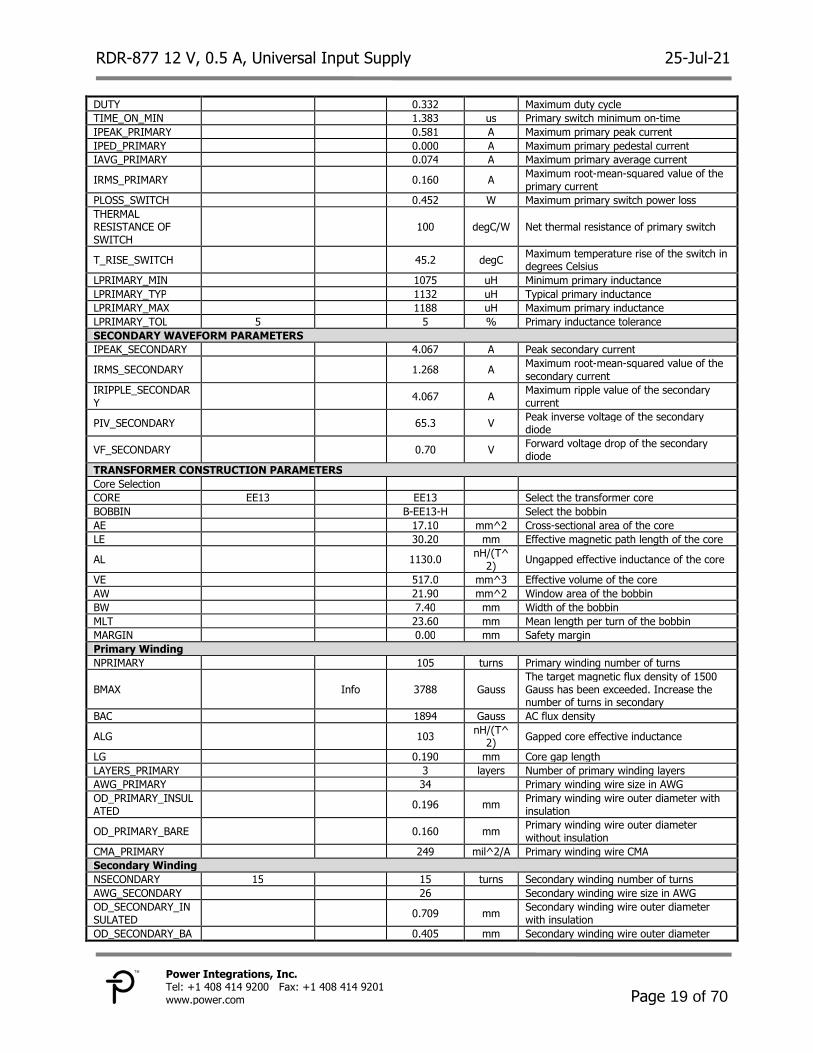
Transformer Design Spreadsheet 9ACDC_LinkSwitchTNZ_Flyback_081420; Rev.0.1; Copyright Power Integrations 2020
INPUT INFO OUTPUT UNIT ACDC LinkSwitch-TNZ Flyback Design Spreadsheet
ENTER APPLICATION VARIABLES
LINE VOLTAGE RANGE
UNIVERSAL
AC line voltage range
VACMIN 90.00
90.00 V Minimum AC line voltage
VACMAX 265.00
265.00 V Maximum AC line voltage
fL
60.00 Hz AC mains frequency
LINE RECTIFICATION TYPE
F
F
Line rectification type: select "F" if full wave rectification or "H" if half wave rectification
VOUT 12.00
12.00 V Output voltage
IOUT 0.500
0.500 A Average output current
EFFICIENCY (User Estimate)
0.80
Overall efficiency estimate. Adjust to match calculated or enter measured efficiency
LOSS ALLOCATION FACTOR
0.50
The ratio of power losses during the primary switch off-state to the total system losses
POUT
6.00 W Continuous output power
CIN 16.80
16.80 uF Input capacitor
VMIN
102.80 V Valley voltage of the rectified minimum AC line voltage
VMAX
374.77 V Peak voltage of the maximum AC line voltage
FEEDBACK BIAS
BIAS
Type of feedback required. Choose "BIAS" for bias winding feedback and "OPTO" for an optocoupler feedback
BIAS WINDING YES
YES
Select whether a bias winding is required or not
INPUT STAGE RESISTANCE
0.0
0.0 Ohms Input stage resistance (includes thermistor, filtering components, etc)
PLOSS_INPUTSTAGE
0.000 W Maximum input stage power loss
LINKSWITCH-TNZ VARIABLES
CURRENT LIMIT MODE
STD
STD
Choose "STD" for Standard current limit or "RED" for reduced current limit
PACKAGE
SO-8C
Device package
DEVICE SERIES LNK3306
LNK3306
Generic LinkSwitch-TNZ device
DEVICE CODE
LNK3306D
Required LinkSwitch-TNZ device
ILIMITMIN
0.450 A Minimum current limit of the device
ILIMITTYP
0.482 A Typical current limit of the device
ILIMITMAX
0.515 A Maximum current limit of the device
RDSON
12.9 Ohms Switch on-state drain-to-source resistance at 100 degC
FSMIN
62000 Hz Minimum switching frequency
FSTYP
66000 Hz Typical switching frequency
FSMAX
70000 Hz Maximum switching frequency
BVDSS
725 V Device breakdown voltage
PRIMARY WAVEFORM PARAMETERS
OPERATION MODE
DCM
Discontinuous mode of operation
VOR 88.5
88.5 V Voltage reflected across the primary winding when the primary switch is off
VDSON
2.00 V Primary switch on-time drain-to-source voltage
VDSOFF
533.3 V Primary switch off-time drain-to-source voltage stress
KRP/KDP
1.770
Degree on how much the operation tend to be continuous or discontinuous
KP_TRANSIENT
0.632
KP value under transient conditions
RDR-877 12 V, 0.5 A, Universal Input Supply 25-Jul-21
Page 19 of 70
Power Integrations, Inc. Tel: +1 408 414 9200 Fax: +1 408 414 9201 www.power.com
DUTY
0.332
Maximum duty cycle
TIME_ON_MIN
1.383 us Primary switch minimum on-time
IPEAK_PRIMARY
0.581 A Maximum primary peak current
IPED_PRIMARY
0.000 A Maximum primary pedestal current
IAVG_PRIMARY
0.074 A Maximum primary average current
IRMS_PRIMARY
0.160 A Maximum root-mean-squared value of the primary current
PLOSS_SWITCH
0.452 W Maximum primary switch power loss
THERMAL RESISTANCE OF SWITCH
100 degC/W Net thermal resistance of primary switch
T_RISE_SWITCH
45.2 degC Maximum temperature rise of the switch in degrees Celsius
LPRIMARY_MIN
1075 uH Minimum primary inductance
LPRIMARY_TYP
1132 uH Typical primary inductance
LPRIMARY_MAX
1188 uH Maximum primary inductance
LPRIMARY_TOL 5
5 % Primary inductance tolerance
SECONDARY WAVEFORM PARAMETERS
IPEAK_SECONDARY
4.067 A Peak secondary current
IRMS_SECONDARY
1.268 A Maximum root-mean-squared value of the secondary current
IRIPPLE_SECONDARY
4.067 A Maximum ripple value of the secondary current
PIV_SECONDARY
65.3 V Peak inverse voltage of the secondary diode
VF_SECONDARY
0.70 V Forward voltage drop of the secondary diode
TRANSFORMER CONSTRUCTION PARAMETERS
Core Selection
CORE EE13
EE13
Select the transformer core
BOBBIN
B-EE13-H
Select the bobbin
AE
17.10 mm^2 Cross-sectional area of the core
LE
30.20 mm Effective magnetic path length of the core
AL
1130.0 nH/(T^
2) Ungapped effective inductance of the core
VE
517.0 mm^3 Effective volume of the core
AW
21.90 mm^2 Window area of the bobbin
BW
7.40 mm Width of the bobbin
MLT
23.60 mm Mean length per turn of the bobbin
MARGIN
0.00 mm Safety margin
Primary Winding
NPRIMARY
105 turns Primary winding number of turns
BMAX
Info 3788 Gauss The target magnetic flux density of 1500 Gauss has been exceeded. Increase the number of turns in secondary
BAC
1894 Gauss AC flux density
ALG
103 nH/(T^
2) Gapped core effective inductance
LG
0.190 mm Core gap length
LAYERS_PRIMARY
3 layers Number of primary winding layers
AWG_PRIMARY
34
Primary winding wire size in AWG
OD_PRIMARY_INSULATED
0.196 mm Primary winding wire outer diameter with insulation
OD_PRIMARY_BARE
0.160 mm Primary winding wire outer diameter without insulation
CMA_PRIMARY
249 mil^2/A Primary winding wire CMA
Secondary Winding
NSECONDARY 15
15 turns Secondary winding number of turns
AWG_SECONDARY
26
Secondary winding wire size in AWG
OD_SECONDARY_INSULATED
0.709 mm Secondary winding wire outer diameter with insulation
OD_SECONDARY_BA
0.405 mm Secondary winding wire outer diameter

RDR-877 12 V, 0.5 A, Universal Input Supply 25-Jul-21
Page 20 of 70
Power Integrations, Inc. Tel: +1 408 414 9200 Fax: +1 408 414 9201 www.power.com
RE without insulation
CMA_SECONDARY
200 mil^2/A Secondary winding wire CMA
Bias Winding
NBIAS
15 turns Bias winding number of turns
VF_BIAS
0.70 V Forward voltage drop of bias diode
VBIAS
12.00 V Voltage across the bias winding
PIV_BIAS
65.25 V Peak inverse voltage on the bias diode
RBP
84500 Ohms BP pin resistor
CBP
0.1 uF BP pin capacitor
Primary Winding Losses
PLOSS_PRIMARYWINDING
0.054 W Maximum power loss dissipated in the primary winding
FEEDBACK PARAMETERS
DIODE_BIAS
1N4003-4007
Recommended bias diode is 1N400X
RUPPER
15000 Ohms Resistor divider component between bias winding and FB pin of LinkSwitch-TNZ
RLOWER
3000 Ohms Resistor divider component between FB pin of LinkSwitch-TNZ and primary RTN
OUTPUT PARAMETERS
VOUT1
12.00 V Output voltage 1
IOUT1
0.500 A Output current 1
POUT1
6.00 W Output power 1
VD1
0.70 V Forward voltage drop of secondary diode for output 1
NS1
15 turns Number of turns for output 1
ISPEAK1
4.07 A Instantaneous peak value of the secondary current for output 1
ISRMS1
1.268 A Root-mean-squared value of the secondary current for output 1
ISRIPPLE1
4.067 A Current ripple on the secondary current waveform for output 1
PIV1_CALCULATED
65.3 V Computed peak inverse voltage stress on the secondary diode for output 1
PIV1_RATING
100 V Peak inverse voltage rating on the secondary diode for output 1
TRR1
25 ns Reverse recovery time of the secondary diode for output 1
IFM1
1.30 A Maximum forward continuous current of the secondary diode for output 1
DIODE1_RECOMMENDED
BYV27-100
Recommended diode for output 1
PLOSS_DIODE1
0.273 W Maximum secondary diode power loss for output 1
VOUT1_RIPPLE
120 mV Output voltage ripple for output 1
ESR_COUT1
30 mOhms Equivalent series resistance of the output capacitor for output 1
IRMS_COUT1
1.165 A Root-mean-squared value of the output capacitor current for output 1
PLOSS_COUT1
0.041 W Maximum output capacitor power loss for output 1
CMS1
254 Cmils Bare conductor effective area in circular mils for output 1
AWGS1
26 AWG Wire size of winding for output 1
ODS1_INSULATED
0.709 mm Secondary winding wire outer diameter with insulation for output 1
ODS1_BARE
0.405 mm Secondary winding wire outer diameter without insulation for output 1
PLOSS_SECONDARYWINDING1
0.076 W Maximum power loss dissipated of secondary winding for output 1

RDR-877 12 V, 0.5 A, Universal Input Supply 25-Jul-21
Page 21 of 70
Power Integrations, Inc. Tel: +1 408 414 9200 Fax: +1 408 414 9201 www.power.com
Performance Data 10
Efficiency 10.1
Active Mode Measurement Data 10.1.1
Measured Performance Standards
VIN (VAC) DOE6 EC CoC (v5)
115 230 2014 2016
Tier 1 Tier 2
Efficiency (%)
Load
(%)
10 74.76 74.70 65.82 69.03
25 77.69 77.86
50 79.97 80.17
75 80.67 80.96
100 80.87 81.29
Ave 79.80 80.07 78.88 75.82 79.03
No-Load Input
Power (mW) 19.17 21.67 100 150 75
Compliant Y Y Y
RDR-877 12 V, 0.5 A, Universal Input Supply 25-Jul-21
Page 22 of 70
Power Integrations, Inc. Tel: +1 408 414 9200 Fax: +1 408 414 9201 www.power.com
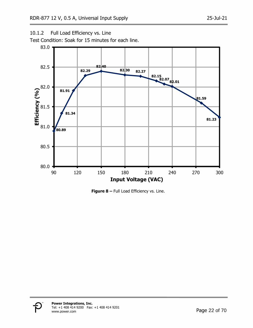
Full Load Efficiency vs. Line 10.1.2
Test Condition: Soak for 15 minutes for each line.
Figure 8 – Full Load Efficiency vs. Line.
80.89
81.34
81.91
82.29
82.4082.30 82.27
82.1582.07
82.01
81.59
81.23
80.0
80.5
81.0
81.5
82.0
82.5
83.0
90 120 150 180 210 240 270 300
Eff
icie
ncy (
%)
Input Voltage (VAC)

RDR-877 12 V, 0.5 A, Universal Input Supply 25-Jul-21
Page 23 of 70
Power Integrations, Inc. Tel: +1 408 414 9200 Fax: +1 408 414 9201 www.power.com
Efficiency vs. Load 10.1.3
Test Condition: Soak for 15 minutes each line, and 5 minutes for each load.
Figure 9 – Efficiency vs. Percentage Load.
50
55
60
65
70
75
80
85
0 10 20 30 40 50 60 70 80 90 100
Eff
icie
ncy (
%)
Load (%)
90 VAC
115 VAC
230 VAC
300 VAC

RDR-877 12 V, 0.5 A, Universal Input Supply 25-Jul-21
Page 24 of 70
Power Integrations, Inc. Tel: +1 408 414 9200 Fax: +1 408 414 9201 www.power.com
Available Standby Output Power 10.2
Figure 10 – Available Standby Output Power for 1 W, 2 W and 3 W Input Power.
0.0
0.5
1.0
1.5
2.0
2.5
3.0
90 120 150 180 210 240 270 300
Inp
ut
Po
wer
(W)
Input Voltage (VAC)
1 W Input
2 W Input
3 W Input

RDR-877 12 V, 0.5 A, Universal Input Supply 25-Jul-21
Page 25 of 70
Power Integrations, Inc. Tel: +1 408 414 9200 Fax: +1 408 414 9201 www.power.com
Figure 11 – Available Standby Output Power for 0.3 W and 0.5 W Input Power.
0.0
0.1
0.2
0.3
0.4
0.5
90 120 150 180 210 240 270 300
Inp
ut
Po
wer
(W)
Input Voltage (VAC)

RDR-877 12 V, 0.5 A, Universal Input Supply 25-Jul-21
Page 26 of 70
Power Integrations, Inc. Tel: +1 408 414 9200 Fax: +1 408 414 9201 www.power.com
No-Load Input Power 10.3
Test Condition: Soak for 15 minutes each line and 1 minute integration time.
Figure 12 – No-Load Input Power vs. Line at Room Temperature.
18.76
19.19 19.3719.66
20.1720.87
21.3321.97 22.22
22.60
23.86
25.27
10.0
12.5
15.0
17.5
20.0
22.5
25.0
27.5
30.0
90 120 150 180 210 240 270 300
Inp
ut
Po
wer
(mW
)
Input Voltage (VAC)

RDR-877 12 V, 0.5 A, Universal Input Supply 25-Jul-21
Page 27 of 70
Power Integrations, Inc. Tel: +1 408 414 9200 Fax: +1 408 414 9201 www.power.com
Line Regulation 10.4
Test Condition: Soak for 15 minutes for each line.
Figure 13 – Output Voltage vs. Line Voltage.
12.41
12.42
11.0
11.3
11.5
11.8
12.0
12.3
12.5
12.8
13.0
90 120 150 180 210 240 270 300
12
V O
utp
ut
(V)
Input Voltage (VAC)

RDR-877 12 V, 0.5 A, Universal Input Supply 25-Jul-21
Page 28 of 70
Power Integrations, Inc. Tel: +1 408 414 9200 Fax: +1 408 414 9201 www.power.com
Load Regulation 10.5
Test Condition: Soak for 15 minutes each line, and 5 minutes for each load.
Figure 14 – Output Voltage vs. Percent Load.
11.0
11.3
11.5
11.8
12.0
12.3
12.5
12.8
13.0
0 10 20 30 40 50 60 70 80 90 100
12
V O
utp
ut
(V)
Load (%)
90 VAC
115 VAC
230 VAC
300 VAC

RDR-877 12 V, 0.5 A, Universal Input Supply 25-Jul-21
Page 29 of 70
Power Integrations, Inc. Tel: +1 408 414 9200 Fax: +1 408 414 9201 www.power.com
Waveforms 11
Zero Crossing Detection 11.1
Zero Crossing Detection at Normal Operation 11.1.1
100% Load 11.1.1.1
Figure 15 – 90 VAC 60 Hz.
CH1: ZCD, 2 V / div., 4 ms / div. CH2: VIN, 100 V / div., 4 ms / div.
Figure 16 – 115 VAC 60 Hz.
CH1: ZCD, 2 V / div., 4 ms / div. CH2: VIN, 100 V / div., 4 ms / div.
Figure 17 – 230 VAC 50 Hz.
CH1: ZCD, 2 V / div., 4 ms / div.
CH2: VIN, 100 V / div., 4 ms / div.
Figure 18 – 300 VAC 50 Hz.
CH1: ZCD, 2 V / div., 4 ms / div.
CH2: VIN, 100 V / div., 4 ms / div.

RDR-877 12 V, 0.5 A, Universal Input Supply 25-Jul-21
Page 30 of 70
Power Integrations, Inc. Tel: +1 408 414 9200 Fax: +1 408 414 9201 www.power.com
0% Load 11.1.1.2
Figure 19 – 90 VAC 60 Hz.
CH1: ZCD, 2 V / div., 4 ms / div.
CH2: VIN, 100 V / div., 4 ms / div.
Figure 20 – 115 VAC 60 Hz.
CH1: ZCD, 2 V / div., 4 ms / div.
CH2: VIN, 100 V / div., 4 ms / div.
Figure 21 – 230 VAC 50 Hz.
CH1: ZCD, 2 V / div., 4 ms / div.
CH2: VIN, 100 V / div., 4 ms / div.
Figure 22 – 300 VAC 50 Hz.
CH1: ZCD, 2 V / div., 4 ms / div.
CH2: VIN, 100 V / div., 4 ms / div.

RDR-877 12 V, 0.5 A, Universal Input Supply 25-Jul-21
Page 31 of 70
Power Integrations, Inc. Tel: +1 408 414 9200 Fax: +1 408 414 9201 www.power.com
Zero Crossing Detection at Start-up 11.1.2
0° Start-up Phase 11.1.2.1
Figure 23 – 115 VAC 60 Hz, No Load
CH1: ZCD, 2 V / div., 4 ms / div.
CH2: VIN, 100 V / div., 4 ms / div.
Figure 24 – 115 VAC 60 Hz, Full Load
CH1: ZCD, 2 V / div., 4 ms / div.
CH2: VIN, 100 V / div., 4 ms / div.
Figure 25 – 230 VAC 50 Hz, No Load
CH1: ZCD, 2 V / div., 4 ms / div. CH2: VIN, 100 V / div., 4 ms / div.
Figure 26 – 230 VAC 50 Hz, Full Load
CH1: ZCD, 2 V / div., 4 ms / div. CH2: VIN, 100 V / div., 4 ms / div.

RDR-877 12 V, 0.5 A, Universal Input Supply 25-Jul-21
Page 32 of 70
Power Integrations, Inc. Tel: +1 408 414 9200 Fax: +1 408 414 9201 www.power.com
90° Start-up Phase 11.1.2.2
Figure 27 – 115 VAC 60 Hz, No Load
CH1: ZCD, 2 V / div., 4 ms / div.
CH2: VIN, 100 V / div., 4 ms / div.
Figure 28 – 115 VAC 60 Hz, Full Load
CH1: ZCD, 2 V / div., 4 ms / div.
CH2: VIN, 100 V / div., 4 ms / div.
Figure 29 – 230 VAC 50 Hz, No Load
CH1: ZCD, 2 V / div., 4 ms / div.
CH2: VIN, 100 V / div., 4 ms / div.
Figure 30 – 230 VAC 50 Hz, Full Load
CH1: ZCD, 2 V / div., 4 ms / div.
CH2: VIN, 100 V / div., 4 ms / div.
RDR-877 12 V, 0.5 A, Universal Input Supply 25-Jul-21
Page 33 of 70
Power Integrations, Inc. Tel: +1 408 414 9200 Fax: +1 408 414 9201 www.power.com
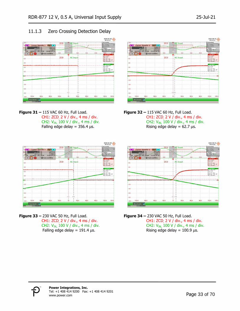
Zero Crossing Detection Delay 11.1.3
Figure 31 – 115 VAC 60 Hz, Full Load.
CH1: ZCD, 2 V / div., 4 ms / div.
CH2: VIN, 100 V / div., 4 ms / div.
Falling edge delay = 356.4 µs.
Figure 32 – 115 VAC 60 Hz, Full Load.
CH1: ZCD, 2 V / div., 4 ms / div.
CH2: VIN, 100 V / div., 4 ms / div.
Rising edge delay = 62.7 µs.
Figure 33 – 230 VAC 50 Hz, Full Load.
CH1: ZCD, 2 V / div., 4 ms / div.
CH2: VIN, 100 V / div., 4 ms / div.
Falling edge delay = 191.4 µs.
Figure 34 – 230 VAC 50 Hz, Full Load.
CH1: ZCD, 2 V / div., 4 ms / div.
CH2: VIN, 100 V / div., 4 ms / div.
Rising edge delay = 100.9 µs.

RDR-877 12 V, 0.5 A, Universal Input Supply 25-Jul-21
Page 34 of 70
Power Integrations, Inc. Tel: +1 408 414 9200 Fax: +1 408 414 9201 www.power.com
Zero Crossing Detection using NPN Solution 11.2
Test Condition: Q1=BC847, R9=10kΩ, R10=10kΩ, Remove VR3
Zero Crossing Detection at Normal Operation 11.2.1
Figure 35 – 115 VAC 60 Hz, No-Load.
CH1: VIN, 100 V / div., 5.2 ms / div. CH2: ZCD, 2 V / div., 5.2 ms / div.
Figure 36 – 115 VAC 60 Hz, Full Load.
CH1: VIN, 100 V / div., 5.2 ms / div. CH2: ZCD, 2 V / div., 5.2 ms / div.
Figure 37 – 230 VAC 50 Hz, No-Load.
CH1: VIN, 100 V / div., 5.2 ms / div.
CH2: ZCD, 2 V / div., 5.2 ms / div.
Figure 38 – 265 VAC 50 Hz, Full Load.
CH1: VIN, 100 V / div., 5.2 ms / div.
CH2: ZCD, 2 V / div., 5.2 ms / div.

RDR-877 12 V, 0.5 A, Universal Input Supply 25-Jul-21
Page 35 of 70
Power Integrations, Inc. Tel: +1 408 414 9200 Fax: +1 408 414 9201 www.power.com
Zero Crossing Detection Delay 11.2.2
Figure 39 – 115 VAC 60 Hz.
CH1: VIN, 100 V / div., 800 µs / div.
CH2: ZCD, 2 V / div., 800 µs / div.
Falling edge delay = 464 µs.
Figure 40 – 115 VAC 60 Hz.
CH1: VIN, 100 V / div., 800 µs / div.
CH2: ZCD, 2 V / div., 800 µs / div.
Rising edge delay = -256 µs.
Figure 41 – 230 VAC 50 Hz.
CH1: VIN, 100 V / div., 800 µs / div.
CH2: ZCD, 2 V / div., 800 µs / div.
Falling edge delay = 240 µs.
Figure 42 – 230 VAC 50 Hz.
CH1: VIN, 100 V / div., 800 µs / div.
CH2: ZCD, 2 V / div., 800 µs / div.
Falling edge delay =-104 µs.

RDR-877 12 V, 0.5 A, Universal Input Supply 25-Jul-21
Page 36 of 70
Power Integrations, Inc. Tel: +1 408 414 9200 Fax: +1 408 414 9201 www.power.com
Load Transient Response 11.3
Test Condition: Dynamic load frequency = 1 kHz, Duty cycle = 50 %
0% - 100% Load Change 11.3.1
Figure 43 – 90 VAC 60 Hz.
CH3: VOUT, 400 mV / div., 500 µs / div.
CH4: IOUT, 200 mA / div., 500 µs / div.
VMAX: 12.449 V, VMIN: 12.354 V.
Figure 44 – 115 VAC 60 Hz.
CH3: VOUT, 400 mV / div., 500 µs / div.
CH4: IOUT, 200 mA / div., 500 µs / div.
VMAX: 12.464 V, VMIN: 12.354 V.
Figure 45 – 230 VAC 50 Hz.
CH3: VOUT, 400 mV / div., 500 µs / div.
CH4: IOUT, 200 mA / div., 500 µs / div.
VMAX: 12.464 V, VMIN: 12.354 V.
Figure 46 – 300 VAC 50 Hz.
CH3: VOUT, 400 mV / div., 500 µs / div.
CH4: IOUT, 200 mA / div., 500 µs / div.
VMAX: 12.464 V, VMIN: 12.354 V.

RDR-877 12 V, 0.5 A, Universal Input Supply 25-Jul-21
Page 37 of 70
Power Integrations, Inc. Tel: +1 408 414 9200 Fax: +1 408 414 9201 www.power.com
50% - 100% Load Change 11.3.2
Figure 47 – 90 VAC 60 Hz.
CH3: VOUT, 400 mV / div., 500 µs / div.
CH4: IOUT, 200 mA / div., 500 µs / div.
VMAX: 12.449 V, VMIN: 12.338 V.
Figure 48 – 115 VAC 60 Hz.
CH3: VOUT, 400 mV / div., 500 µs / div.
CH4: IOUT, 200 mA / div., 500 µs / div.
VMAX: 12.449 V, VMIN: 12.354 V.
Figure 49 – 230 VAC 50 Hz.
CH3: VOUT, 400 mV / div., 500 µs / div.
CH4: IOUT, 200 mA / div., 500 µs / div.
VMAX: 12.449 V, VMIN: 12.354 V.
Figure 50 – 300 VAC 50 Hz.
CH3: VOUT, 400 mV / div., 500 µs / div.
CH4: IOUT, 200 mA / div., 500 µs / div.
VMAX: 12.449 V, VMIN: 12.354 V.

RDR-877 12 V, 0.5 A, Universal Input Supply 25-Jul-21
Page 38 of 70
Power Integrations, Inc. Tel: +1 408 414 9200 Fax: +1 408 414 9201 www.power.com
Output Voltage at Start-up 11.4
CC Mode 11.4.1
100% Load 11.4.1.1
Figure 51 – 90 VAC 60 Hz.
CH2: VIN, 500 V / div., 10 ms / div. CH3: VOUT, 5 V / div., 10 ms / div.
CH4: IOUT, 250 mA / div., 10 ms / div.
Rise Time = 14.654 ms.
Figure 52 – 115 VAC 60 Hz.
CH2: VIN, 500 V / div., 10 ms / div. CH3: VOUT, 5 V / div., 10 ms / div.
CH4: IOUT, 250 mA / div., 10 ms / div.
Rise Time = 13.751 ms.
Figure 53 – 230 VAC 50 Hz.
CH2: VIN, 500 V / div., 10 ms / div.
CH3: VOUT, 5 V / div., 10 ms / div.
CH4: IOUT, 250 mA / div., 10 ms / div. Rise Time = 11.01 ms.
Figure 54 – 300 VAC 50 Hz.
CH2: VIN, 500 V / div., 10 ms / div.
CH3: VOUT, 5 V / div., 10 ms / div.
CH4: IOUT, 250 mA / div., 10 ms / div. Rise Time = 9.6776 ms.

RDR-877 12 V, 0.5 A, Universal Input Supply 25-Jul-21
Page 39 of 70
Power Integrations, Inc. Tel: +1 408 414 9200 Fax: +1 408 414 9201 www.power.com
0% Load 11.4.1.2
Figure 55 – 90 VAC 60 Hz.
CH2: VIN, 500 V / div., 10 ms / div.
CH3: VOUT, 5 V / div., 10 ms / div.
CH4: IOUT, 250 mA / div., 10 ms / div. Rise Time = 7.7242 ms.
Figure 56 – 115 VAC 60 Hz.
CH2: VIN, 500 V / div., 10 ms / div.
CH3: VOUT, 5 V / div., 10 ms / div.
CH4: IOUT, 250 mA / div., 10 ms / div. Rise Time = 7.4095 ms.
Figure 57 – 230 VAC 50 Hz.
CH2: VIN, 500 V / div., 10 ms / div.
CH3: VOUT, 5 V / div., 10 ms / div. CH4: IOUT, 250 mA / div., 10 ms / div.
Rise Time = 6.6176 ms.
Figure 58 – 300 VAC 50 Hz.
CH2: VIN, 500 V / div., 10 ms / div.
CH3: VOUT, 5 V / div., 10 ms / div. CH4: IOUT, 250 mA / div., 10 ms / div.
Rise Time = 6.196 ms.

RDR-877 12 V, 0.5 A, Universal Input Supply 25-Jul-21
Page 40 of 70
Power Integrations, Inc. Tel: +1 408 414 9200 Fax: +1 408 414 9201 www.power.com
CR Mode 11.4.2
100% Load 11.4.2.1
Figure 59 – 90 VAC 60 Hz.
CH2: VIN, 500 V / div., 10 ms / div.
CH3: VOUT, 5 V / div., 10 ms / div. CH4: IOUT, 250 mA / div., 10 ms / div.
Rise Time = 11.934 ms.
Figure 60 – 115 VAC 60 Hz.
CH2: VIN, 500 V / div., 10 ms / div.
CH3: VOUT, 5 V / div., 10 ms / div. CH4: IOUT, 250 mA / div., 10 ms / div.
Rise Time = 10.87 ms.
Figure 61 – 230 VAC 50 Hz.
CH2: VIN, 500 V / div., 10 ms / div. CH3: VOUT, 5 V / div., 10 ms / div.
CH4: IOUT, 250 mA / div., 10 ms / div.
Rise Time = 9.4165 ms.
Figure 62 – 300 VAC 50 Hz.
CH2: VIN, 500 V / div., 10 ms / div. CH3: VOUT, 5 V / div., 10 ms / div.
CH4: IOUT, 250 mA / div., 10 ms / div.
Rise Time = 8.5447 ms.

RDR-877 12 V, 0.5 A, Universal Input Supply 25-Jul-21
Page 41 of 70
Power Integrations, Inc. Tel: +1 408 414 9200 Fax: +1 408 414 9201 www.power.com
0% Load 11.4.2.2
Figure 63 – 90 VAC 60 Hz.
CH2: VIN, 500 V / div., 10 ms / div.
CH3: VOUT, 5 V / div., 10 ms / div.
CH4: IOUT, 250 mA / div., 10 ms / div. Rise Time = 7.6843 ms.
Figure 64 – 115 VAC 60 Hz.
CH2: VIN, 500 V / div., 10 ms / div.
CH3: VOUT, 5 V / div., 10 ms / div.
CH4: IOUT, 250 mA / div., 10 ms / div. Rise Time = 7.4422 ms.
Figure 65 – 230 VAC 50 Hz.
CH2: VIN, 500 V / div., 10 ms / div.
CH3: VOUT, 5 V / div., 10 ms / div. CH4: IOUT, 250 mA / div., 10 ms / div.
Rise Time = 6.6378 ms.
Figure 66 – 265 VAC 50 Hz.
CH2: VIN, 500 V / div., 10 ms / div.
CH3: VOUT, 5 V / div., 10 ms / div. CH4: IOUT, 250 mA / div., 10 ms / div.
Rise Time = 6.2406 ms.

RDR-877 12 V, 0.5 A, Universal Input Supply 25-Jul-21
Page 42 of 70
Power Integrations, Inc. Tel: +1 408 414 9200 Fax: +1 408 414 9201 www.power.com
Switching Waveforms 11.5
Primary MOSFET Drain-Source Voltage and Current at Normal Operation 11.5.1
100% Load 11.5.1.1
Figure 67 – 90 VAC 60 Hz.
CH2: VDS, 200 V / div., 10 µs / div.
CH3: IDS, 200 mA / div., 10 µs / div.
VDS(MAX) = 292.49 V.
IDS(MAX) = 507.51 mA.
Figure 68 – 115 VAC 60 Hz.
CH2: VDS, 200 V / div., 10 µs / div.
CH3: IDS, 200 mA / div., 10 µs / div.
VDS(MAX) = 324.11 V.
IDS(MAX) = 515.42 mA.
Figure 69 – 230 VAC 50 Hz.
CH2: VDS, 200 V / div., 10 µs / div.
CH3: IDS, 200 mA / div., 10 µs / div.
VDS(MAX) = 490.12 V. IDS(MAX) = 547.04 mA.
Figure 70 – 300 VAC 50 Hz.
CH2: VDS, 200 V / div., 10 µs / div.
CH3: IDS, 200 mA / div., 10 µs / div.
VDS(MAX) = 600.79 V. IDS(MAX) = 570.75 mA.

RDR-877 12 V, 0.5 A, Universal Input Supply 25-Jul-21
Page 43 of 70
Power Integrations, Inc. Tel: +1 408 414 9200 Fax: +1 408 414 9201 www.power.com
0% Load 11.5.1.2
Figure 71 – 90 VAC 60 Hz.
CH2: VDS, 200 V / div., 10 µs / div.
CH3: IDS, 200 mA / div., 10 µs / div.
VDS(MAX) = 260.87 V. IDS(MAX) = 515.42 mA.
Figure 72 – 115 VAC 60 Hz.
CH2: VDS, 200 V / div., 10 µs / div.
CH3: IDS, 200 mA / div., 10 µs / div.
VDS(MAX) = 300.40 V. IDS(MAX) = 523.32 mA.
Figure 73 – 230 VAC 50 Hz.
CH2: VDS, 200 V / div., 10 µs / div.
CH3: IDS, 200 mA / div., 10 µs / div.
VDS(MAX) = 474.31 V.
IDS(MAX) = 547.04 mA.
Figure 74 – 300 VAC 50 Hz.
CH2: VDS, 200 V / div., 10 µs / div.
CH3: IDS, 200 mA / div., 10 µs / div.
VDS(MAX) = 569.17 V.
IDS(MAX) = 562.85 mA.
RDR-877 12 V, 0.5 A, Universal Input Supply 25-Jul-21
Page 44 of 70
Power Integrations, Inc. Tel: +1 408 414 9200 Fax: +1 408 414 9201 www.power.com
Primary MOSFET Drain-Source Voltage and Current at Start-up Operation 11.5.2
100% Load 11.5.2.1
Figure 75 – 90 VAC 60 Hz.
CH2: VDS, 200 V / div., 10 ms / div.
CH3: IDS, 200 mA / div., 10 ms / div. VDS(MAX) = 284.58 V.
IDS(MAX) = 515.42 mA.
Figure 76 – 115 VAC 60 Hz.
CH2: VDS, 200 V / div., 10 ms / div.
CH3: IDS, 200 mA / div., 10 ms / div. VDS(MAX) = 316.21 V.
IDS(MAX) = 515.42 mA.
Figure 77 – 230 VAC 50 Hz.
CH2: VDS, 200 V / div., 10 ms / div. CH3: IDS, 200 mA / div., 10 ms / div.
VDS(MAX) = 490.12 V.
IDS(MAX) = 547.04 mA.
Figure 78 – 300 VAC 50 Hz.
CH2: VDS, 200 V / div., 10 ms / div. CH3: IDS, 200 mA / div., 10 ms / div.
VDS(MAX) = 600.79 V.
IDS(MAX) = 562.85 mA.
RDR-877 12 V, 0.5 A, Universal Input Supply 25-Jul-21
Page 45 of 70
Power Integrations, Inc. Tel: +1 408 414 9200 Fax: +1 408 414 9201 www.power.com
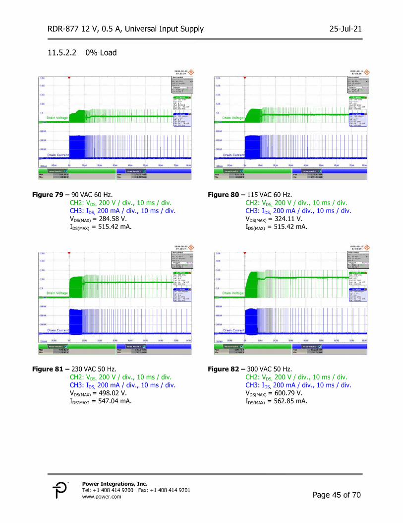
0% Load 11.5.2.2
Figure 79 – 90 VAC 60 Hz.
CH2: VDS, 200 V / div., 10 ms / div.
CH3: IDS, 200 mA / div., 10 ms / div.
VDS(MAX) = 284.58 V. IDS(MAX) = 515.42 mA.
Figure 80 – 115 VAC 60 Hz.
CH2: VDS, 200 V / div., 10 ms / div.
CH3: IDS, 200 mA / div., 10 ms / div.
VDS(MAX) = 324.11 V. IDS(MAX) = 515.42 mA.
Figure 81 – 230 VAC 50 Hz.
CH2: VDS, 200 V / div., 10 ms / div.
CH3: IDS, 200 mA / div., 10 ms / div. VDS(MAX) = 498.02 V.
IDS(MAX) = 547.04 mA.
Figure 82 – 300 VAC 50 Hz.
CH2: VDS, 200 V / div., 10 ms / div.
CH3: IDS, 200 mA / div., 10 ms / div. VDS(MAX) = 600.79 V.
IDS(MAX) = 562.85 mA.

RDR-877 12 V, 0.5 A, Universal Input Supply 25-Jul-21
Page 46 of 70
Power Integrations, Inc. Tel: +1 408 414 9200 Fax: +1 408 414 9201 www.power.com
Output Diode Voltage and Current at Normal Operation 11.5.3
100% Load 11.5.3.1
Figure 83 – 90 VAC 60 Hz.
CH2: VD, 20 V / div., 20 µs / div.
CH3: ID, 2 A / div., 20 µs / div.
PIV = 34.783 V.
ID(MAX) = 4.2846 A.
Figure 84 – 115 VAC 60 Hz.
CH2: VD, 20 V / div., 20 µs / div.
CH3: ID, 2 A / div., 20 µs / div.
PIV = 39.526 V.
ID(MAX) = 4.3636 A.
Figure 85 – 230 VAC 50 Hz.
CH2: VD, 20 V / div., 20 µs / div.
CH3: ID, 2 A / div., 20 µs / div.
PIV = 64.032 V.
ID(MAX) = 4.6798 A.
Figure 86 – 300 VAC 50 Hz.
CH2: VD, 20 V / div., 20 µs / div.
CH3: ID, 2 A / div., 20 µs / div.
PIV = 78.261 V.
ID(MAX) = 4.917 A.

RDR-877 12 V, 0.5 A, Universal Input Supply 25-Jul-21
Page 47 of 70
Power Integrations, Inc. Tel: +1 408 414 9200 Fax: +1 408 414 9201 www.power.com
0% Load 11.5.3.2
Figure 87 – 90 VAC 60 Hz.
CH2: VD, 20 V / div., 20 µs / div.
CH3: ID, 2 A / div., 20 µs / div.
PIV = 33.202 V. ID(MAX) = 2.3083 A.
Figure 88 – 115 VAC 60 Hz.
CH2: VD, 20 V / div., 20 µs / div.
CH3: ID, 2 A / div., 20 µs / div.
PIV = 39.526 V. ID(MAX) = 2.5455 A.
Figure 89 – 230 VAC 50 Hz.
CH2: VD, 20 V / div., 20 µs / div.
CH3: ID, 2 A / div., 20 µs / div.
PIV = 64.822 V.
ID(MAX) = 2.7036 A.
Figure 90 – 300 VAC 50 Hz.
CH2: VD, 20 V / div., 20 µs / div.
CH3: ID, 2 A / div., 20 µs / div.
PIV = 78.261 V.
ID(MAX) = 2.8617 A.

RDR-877 12 V, 0.5 A, Universal Input Supply 25-Jul-21
Page 48 of 70
Power Integrations, Inc. Tel: +1 408 414 9200 Fax: +1 408 414 9201 www.power.com
Output Diode Voltage and Current at Start-up Operation 11.5.4
100% Load 11.5.4.1
Figure 91 – 90 VAC 60 Hz.
CH2: VD, 20 V / div., 10 ms / div.
CH3: ID, 2 A / div., 10 ms / div. PIV = 34.783 V.
ID(MAX) = 4.6798 A.
Figure 92 – 115 VAC 60 Hz.
CH2: VD, 20 V / div., 10 ms / div.
CH3: ID, 2 A / div., 10 ms / div. PIV = 39.526 V.
ID(MAX) = 4.6798 A.
Figure 93 – 230 VAC 50 Hz.
CH2: VD, 20 V / div., 10 ms / div. CH3: ID, 2 A / div., 10 ms / div.
PIV = 64.822 V.
ID(MAX) = 4.917 A.
Figure 94 – 300 VAC 50 Hz.
CH2: VD, 20 V / div., 10 ms / div. CH3: ID, 2 A / div., 10 ms / div.
PIV = 79.842 V.
ID(MAX) = 5.0751 A.

RDR-877 12 V, 0.5 A, Universal Input Supply 25-Jul-21
Page 49 of 70
Power Integrations, Inc. Tel: +1 408 414 9200 Fax: +1 408 414 9201 www.power.com
0% Load 11.5.4.2
Figure 95 – 90 VAC 60 Hz.
CH2: VD, 20 V / div., 10 ms / div.
CH3: ID, 2 A / div., 10 ms / div.
PIV = 33.202 V. ID(MAX) = 4.5217 A.
Figure 96 – 115 VAC 60 Hz.
CH2: VD, 20 V / div., 10 ms / div.
CH3: ID, 2 A / div., 10 ms / div.
PIV = 37.945 V. ID(MAX) = 4.5217 A.
Figure 97 – 230 VAC 50 Hz.
CH2: VD, 20 V / div., 10 ms / div.
CH3: ID, 2 A / div., 10 ms / div. PIV = 64.032 V.
ID(MAX) = 4.7589 A.
Figure 98 – 300 VAC 50 Hz.
CH2: VD, 20 V / div., 10 ms / div.
CH3: ID, 2 A / div., 10 ms / div. PIV = 79.842 V.
ID(MAX) = 4.8379 A.

RDR-877 12 V, 0.5 A, Universal Input Supply 25-Jul-21
Page 50 of 70
Power Integrations, Inc. Tel: +1 408 414 9200 Fax: +1 408 414 9201 www.power.com
Brown-In and Brown-Out 11.6
Brown-in 11.6.1
Figure 99 – Brown-in, Full Load.
CH1: VOUT, 10 V / div., 100 s / div. CH2: VIN, 200 V / div., 100 s / div.
CH3: IOUT, 500 mA / div., 100 s / div. CH4: VDS, 200 V / div., 100 s / div.
Figure 100 – Brown-in, No Load.
CH1: VOUT, 10 V / div., 100 s / div. CH2: VIN, 200 V / div., 100 s / div.
CH3: IOUT, 500 mA / div., 100 s / div. CH4: VDS, 200 V / div., 100 s / div.
Brown-out 11.6.2
Figure 101 – Brown-out, Full Load. CH1: VOUT, 10 V / div., 100 s / div.
CH2: VIN, 200 V / div., 100 s / div.
CH3: IOUT, 500 mA / div., 100 s / div. CH4: VDS, 200 V / div., 100 s / div.
Figure 102 – Brown-out, No Load. CH1: VOUT, 10 V / div., 100 s / div.
CH2: VIN, 200 V / div., 100 s / div.
CH3: IOUT, 500 mA / div., 100 s / div. CH4: VDS, 200 V / div., 100 s / div.

RDR-877 12 V, 0.5 A, Universal Input Supply 25-Jul-21
Page 51 of 70
Power Integrations, Inc. Tel: +1 408 414 9200 Fax: +1 408 414 9201 www.power.com
Fault Conditions 11.7
Output Overvoltage 11.7.1
100% Load 11.7.1.1
Figure 103 – 90 VAC 60 Hz.
CH2: VDS, 400 V / div., 100 ms / div. CH3: IDS, 400 mA / div., 100 ms / div.
CH4: VOUT, 5 V / div., 100 ms / div.
VOUT(MAX) = 14.723 V.
Figure 104 – 115 VAC 60 Hz.
CH2: VDS, 400 V / div., 100 ms / div. CH3: IDS, 400 mA / div., 100 ms / div.
CH4: VOUT, 5 V / div., 100 ms / div.
VOUT(MAX) = 14.723 V.
Figure 105 – 230 VAC 50 Hz.
CH2: VDS, 400 V / div., 100 ms / div.
CH3: IDS, 400 mA / div., 100 ms / div.
CH4: VOUT, 5 V / div., 100 ms / div. VOUT(MAX) = 13.538 V.
Figure 106 – 300 VAC 50 Hz.
CH2: VDS, 400 V / div., 100 ms / div.
CH3: IDS, 400 mA / div., 100 ms / div.
CH4: VOUT, 5 V / div., 100 ms / div. VOUT(MAX) = 13.142 V.

RDR-877 12 V, 0.5 A, Universal Input Supply 25-Jul-21
Page 52 of 70
Power Integrations, Inc. Tel: +1 408 414 9200 Fax: +1 408 414 9201 www.power.com
0% Load 11.7.1.2
Figure 107 – 90 VAC 60 Hz.
CH2: VDS, 400 V / div., 100 ms / div.
CH3: IDS, 400 mA / div., 100 ms / div.
CH4: VOUT, 5 V / div., 100 ms / div. VOUT(MAX) = 15.711 V.
Figure 108 – 115 VAC 60 Hz.
CH2: VDS, 400 V / div., 100 ms / div.
CH3: IDS, 400 mA / div., 100 ms / div.
CH4: VOUT, 5 V / div., 100 ms / div. VOUT(MAX) = 15.514 V.
Figure 109 – 230 VAC 50 Hz.
CH2: VDS, 400 V / div., 100 ms / div.
CH3: IDS, 400 mA / div., 100 ms / div. CH4: VOUT, 5 V / div., 100 ms / div.
VOUT(MAX) = 14.921 V.
Figure 110 – 300 VAC 50 Hz.
CH2: VDS, 400 V / div., 100 ms / div.
CH3: IDS, 400 mA / div., 100 ms / div. CH4: VOUT, 5 V / div., 100 ms / div.
VOUT(MAX) = 14.723 V.

RDR-877 12 V, 0.5 A, Universal Input Supply 25-Jul-21
Page 53 of 70
Power Integrations, Inc. Tel: +1 408 414 9200 Fax: +1 408 414 9201 www.power.com
Output Short-Circuit 11.7.2
Test Condition: Short-circuit applied at normal operation
Figure 111 – 115 VAC 60 Hz.
CH2: VDS, 400 V / div., 100 ms / div.
CH3: IDS, 400 mA / div., 100 ms / div. CH4: VOUT, 5 V / div., 100 ms / div.
VDS(MAX) = 338.34 V.
IDS(MAX) = 0.542 A.
Figure 112 – 230 VAC 50 Hz.
CH2: VDS, 400 V / div., 100 ms / div.
CH3: IDS, 400 mA / div., 100 ms / div. CH4: VOUT, 5 V / div., 100 ms / div.
VDS(MAX) = 559.68 V.
IDS(MAX) = 1.3328 A.

RDR-877 12 V, 0.5 A, Universal Input Supply 25-Jul-21
Page 54 of 70
Power Integrations, Inc. Tel: +1 408 414 9200 Fax: +1 408 414 9201 www.power.com
Output Voltage Ripple 11.8
Ripple Measurement Technique 11.8.1
For DC output ripple measurements, a modified oscilloscope test probe must be utilized in order to reduce spurious signals due to pick-up. Details of the probe modification are provided in the Figures below. The 4987BA probe adapter is affixed with two capacitors tied in parallel across the probe
tip. The capacitors include one (1) 0.1 µF / 50 V ceramic type and one (1) 47 µF / 50 V aluminum electrolytic. The aluminum electrolytic type capacitor is polarized, so proper polarity across DC outputs must be maintained (see below).
Figure 113 – Oscilloscope Probe Prepared for Ripple Measurement. (End Cap and Ground Lead Removed.)
Figure 114 – Oscilloscope Probe with Probe Master (www.probemaster.com) 4987A BNC Adapter. (Modified with wires for ripple measurement, and two parallel decoupling capacitors added.)
Probe Ground
Probe Tip

RDR-877 12 V, 0.5 A, Universal Input Supply 25-Jul-21
Page 55 of 70
Power Integrations, Inc. Tel: +1 408 414 9200 Fax: +1 408 414 9201 www.power.com
Measurement Results 11.8.2
100% Load Condition 11.8.2.1
Figure 115 – 90 VAC 60 Hz.
CH4: VOUT, 40 mV / div., 4 ms / div.
Zoom: 20 µs / div.
Output Ripple = 61.66 mV.
Figure 116 – 115 VAC 60 Hz.
CH4: VOUT, 40 mV / div., 4 ms / div.
Zoom: 20 µs / div.
Output Ripple = 60.079 mV.
Figure 117 – 230 VAC 50 Hz.
CH4: VOUT, 40 mV / div., 4 ms / div.
Zoom: 20 µs / div.
Output Ripple = 63.241 mV.
Figure 118 – 300 VAC 50 Hz.
CH4: VOUT, 40 mV / div., 4 ms / div.
Zoom: 20 µs / div.
Output Ripple = 69.565 mV.

RDR-877 12 V, 0.5 A, Universal Input Supply 25-Jul-21
Page 56 of 70
Power Integrations, Inc. Tel: +1 408 414 9200 Fax: +1 408 414 9201 www.power.com
75% Load Condition 11.8.2.2
Figure 119 – 90 VAC 60 Hz.
CH4: VOUT, 40 mV / div., 4 ms / div.
Zoom: 20 µs / div.
Output Ripple = 61.66 mV.
Figure 120 – 115 VAC 60 Hz.
CH4: VOUT, 40 mV / div., 4 ms / div.
Zoom: 20 µs / div.
Output Ripple = 61.66 mV.
Figure 121 – 230 VAC 50 Hz.
CH4: VOUT, 40 mV / div., 4 ms / div.
Zoom: 20 µs / div.
Output Ripple = 63.241 mV.
Figure 122 – 265 VAC 50 Hz.
CH4: VOUT, 40 mV / div., 4 ms / div.
Zoom: 20 µs / div.
Output Ripple = 67.984 mV.
RDR-877 12 V, 0.5 A, Universal Input Supply 25-Jul-21
Page 57 of 70
Power Integrations, Inc. Tel: +1 408 414 9200 Fax: +1 408 414 9201 www.power.com
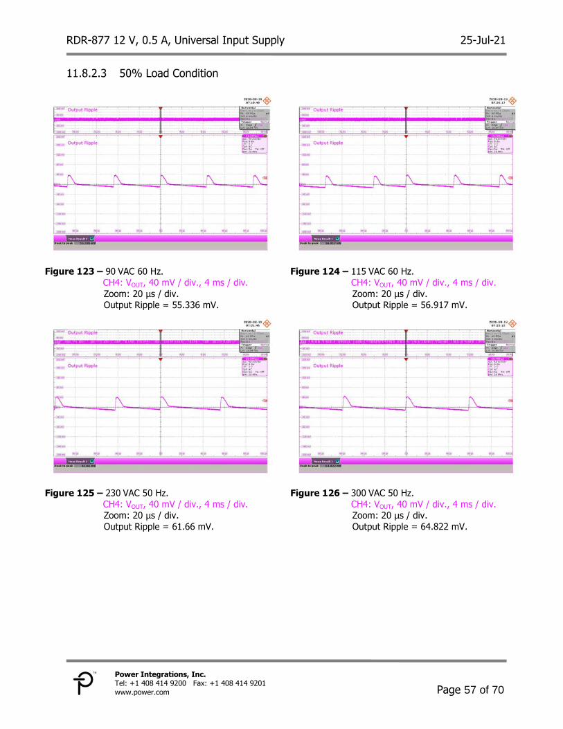
50% Load Condition 11.8.2.3
Figure 123 – 90 VAC 60 Hz.
CH4: VOUT, 40 mV / div., 4 ms / div.
Zoom: 20 µs / div.
Output Ripple = 55.336 mV.
Figure 124 – 115 VAC 60 Hz.
CH4: VOUT, 40 mV / div., 4 ms / div.
Zoom: 20 µs / div.
Output Ripple = 56.917 mV.
Figure 125 – 230 VAC 50 Hz.
CH4: VOUT, 40 mV / div., 4 ms / div.
Zoom: 20 µs / div.
Output Ripple = 61.66 mV.
Figure 126 – 300 VAC 50 Hz.
CH4: VOUT, 40 mV / div., 4 ms / div.
Zoom: 20 µs / div.
Output Ripple = 64.822 mV.

RDR-877 12 V, 0.5 A, Universal Input Supply 25-Jul-21
Page 58 of 70
Power Integrations, Inc. Tel: +1 408 414 9200 Fax: +1 408 414 9201 www.power.com
25% Load Condition 11.8.2.4
Figure 127 – 90 VAC 60 Hz.
CH4: VOUT, 40 mV / div., 4 ms / div.
Zoom: 20 µs / div.
Output Ripple = 53.755 mV.
Figure 128 – 115 VAC 60 Hz.
CH4: VOUT, 40 mV / div., 4 ms / div.
Zoom: 20 µs / div.
Output Ripple = 53.755 mV.
Figure 129 – 230 VAC 50 Hz.
CH4: VOUT, 40 mV / div., 4 ms / div.
Zoom: 20 µs / div.
Output Ripple = 60.079 mV.
Figure 130 – 300 VAC 50 Hz.
CH4: VOUT, 40 mV / div., 4 ms / div.
Zoom: 20 µs / div.
Output Ripple = 61.66 mV.

RDR-877 12 V, 0.5 A, Universal Input Supply 25-Jul-21
Page 59 of 70
Power Integrations, Inc. Tel: +1 408 414 9200 Fax: +1 408 414 9201 www.power.com
0% Load Condition 11.8.2.5
Figure 131 – 90 VAC 60 Hz.
CH4: VOUT, 40 mV / div., 4 ms / div.
Zoom: 20 µs / div.
Output Ripple = 41.107 mV.
Figure 132 – 115 VAC 60 Hz.
CH4: VOUT, 40 mV / div., 4 ms / div.
Zoom: 20 µs / div.
Output Ripple = 53.755 mV.
Figure 133 – 230 VAC 50 Hz.
CH4: VOUT, 40 mV / div., 4 ms / div.
Zoom: 20 µs / div.
Output Ripple = 56.917 mV.
Figure 134 – 300 VAC 50 Hz.
CH4: VOUT, 40 mV / div., 4 ms / div.
Zoom: 20 µs / div.
Output Ripple = 60.079 mV.

RDR-877 12 V, 0.5 A, Universal Input Supply 25-Jul-21
Page 60 of 70
Power Integrations, Inc. Tel: +1 408 414 9200 Fax: +1 408 414 9201 www.power.com
Output Ripple Voltage Graph from 0% - 100% 11.8.3
Figure 135 – Measured at the Board Output Terminals at Room Temperature.
50
55
60
65
70
0 10 20 30 40 50 60 70 80 90 100
Rip
ple
(m
V)
Load (%)
90 VAC
115 VAC
230 VAC
300 VAC

RDR-877 12 V, 0.5 A, Universal Input Supply 25-Jul-21
Page 61 of 70
Power Integrations, Inc. Tel: +1 408 414 9200 Fax: +1 408 414 9201 www.power.com
Thermal Performance 12
Test Set-Up 12.1
Thermal evaluation was performed room temperature with the circuit board enclosed inside an acrylic box.
Figure 136 – Thermal Performance Set-up Using an Acrylic Box.

RDR-877 12 V, 0.5 A, Universal Input Supply 25-Jul-21
Page 62 of 70
Power Integrations, Inc. Tel: +1 408 414 9200 Fax: +1 408 414 9201 www.power.com
Thermal Performance at Room Temperature 12.2
90 VAC at Room Temperature 12.2.1
Figure 137 – Thermal Performance at 90 VAC, Bottom Side.
Figure 138 – Thermal Performance at 90 VAC, Top Side
.
Component Temperature (°C)
LNK3306D (U1) 62.0
Snubber Resistor (R2) 60.3
Output Diode (D1) 66.5
Snubber Diode (D2) 63.5
Transformer (T1) 60.4
Output Capacitor (C5) 50.5
Ambient 25.0

RDR-877 12 V, 0.5 A, Universal Input Supply 25-Jul-21
Page 63 of 70
Power Integrations, Inc. Tel: +1 408 414 9200 Fax: +1 408 414 9201 www.power.com
115 VAC at Room Temperature 12.2.2
Figure 139 – Thermal Performance at 90 VAC, Bottom Side.
Figure 140 – Thermal Performance at 115 VAC, Top Side.
Component Temperature (°C)
LNK3306D (U1) 58.1
Snubber Resistor (R2) 57.4
Output Diode (D1) 68.1
Snubber Diode (D2) 61.0
Transformer (T1) 60.7
Output Capacitor (C5) 53.6
Ambient 25.0

RDR-877 12 V, 0.5 A, Universal Input Supply 25-Jul-21
Page 64 of 70
Power Integrations, Inc. Tel: +1 408 414 9200 Fax: +1 408 414 9201 www.power.com
230 VAC at Room Temperature 12.2.3
Figure 141 – Thermal Performance at 230 VAC, Bottom Side.
Figure 142 – Thermal Performance at 230 VAC, Top Side.
Component Temperature (°C)
LNK3306D (U1) 58.1
Snubber Resistor (R2) 57.4
Output Diode (D1) 68.1
Snubber Diode (D2) 61.0
Transformer (T1) 60.7
Output Capacitor (C5) 52.3
Ambient 25.0

RDR-877 12 V, 0.5 A, Universal Input Supply 25-Jul-21
Page 65 of 70
Power Integrations, Inc. Tel: +1 408 414 9200 Fax: +1 408 414 9201 www.power.com
300 VAC at Room Temperature 12.2.4
Figure 143 – Thermal Performance at 300 VAC, Bottom Side.
Figure 144 – Thermal Performance at 300 VAC, Top Side.
Component Temperature (°C)
LNK3306D (U1) 61.7
Snubber Resistor (R2) 58.5
Output Diode (D1) 69.5
Snubber Diode (D2) 62.2
Transformer (T1) 62.1
Output Capacitor (C5) 52.9
Ambient 25.0

RDR-877 12 V, 0.5 A, Universal Input Supply 25-Jul-21
Page 66 of 70
Power Integrations, Inc. Tel: +1 408 414 9200 Fax: +1 408 414 9201 www.power.com
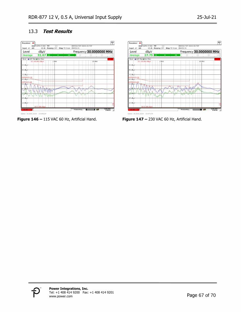
Conducted EMI 13
Conducted emissions tests were performed at 115 VAC and 230 VAC at full load (12 V, 1 A). Measurements were taken with an Artificial Hand connected and a floating DC output load resistor. A DC output cable was included.
Test Set-up Equipment 13.1
Equipment and Load Used 13.1.1
1. Rohde and Schwarz ENV216 two line V-network. 2. Rohde and Schwarz ESRP EMI test receiver. 3. Hioki 3322 power Hi-tester. 4. Chroma measurement test fixture. 5. Input voltage set at 115 VAC and 230 VAC.
Test Set-up 13.2
Figure 145 – EMI Test Set-up.
RDR-877 12 V, 0.5 A, Universal Input Supply 25-Jul-21
Page 67 of 70
Power Integrations, Inc. Tel: +1 408 414 9200 Fax: +1 408 414 9201 www.power.com
Test Results 13.3
Figure 146 – 115 VAC 60 Hz, Artificial Hand. Figure 147 – 230 VAC 60 Hz, Artificial Hand.
RDR-877 12 V, 0.5 A, Universal Input Supply 25-Jul-21
Page 68 of 70
Power Integrations, Inc. Tel: +1 408 414 9200 Fax: +1 408 414 9201 www.power.com
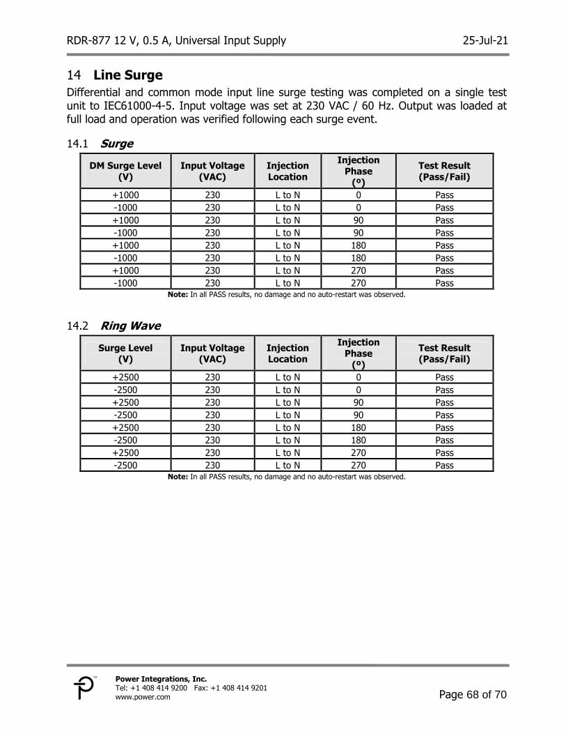
Line Surge 14
Differential and common mode input line surge testing was completed on a single test unit to IEC61000-4-5. Input voltage was set at 230 VAC / 60 Hz. Output was loaded at full load and operation was verified following each surge event.
Surge 14.1
DM Surge Level
(V)
Input Voltage
(VAC)
Injection
Location
Injection
Phase (º)
Test Result
(Pass/Fail)
+1000 230 L to N 0 Pass
-1000 230 L to N 0 Pass
+1000 230 L to N 90 Pass
-1000 230 L to N 90 Pass
+1000 230 L to N 180 Pass
-1000 230 L to N 180 Pass
+1000 230 L to N 270 Pass
-1000 230 L to N 270 Pass Note: In all PASS results, no damage and no auto-restart was observed.
Ring Wave 14.2
Surge Level (V)
Input Voltage (VAC)
Injection Location
Injection
Phase (º)
Test Result (Pass/Fail)
+2500 230 L to N 0 Pass
-2500 230 L to N 0 Pass
+2500 230 L to N 90 Pass
-2500 230 L to N 90 Pass
+2500 230 L to N 180 Pass
-2500 230 L to N 180 Pass
+2500 230 L to N 270 Pass
-2500 230 L to N 270 Pass Note: In all PASS results, no damage and no auto-restart was observed.

RDR-877 12 V, 0.5 A, Universal Input Supply 25-Jul-21
Page 69 of 70
Power Integrations, Inc. Tel: +1 408 414 9200 Fax: +1 408 414 9201 www.power.com
Revision History 15
Date Author Revision Description and Changes Reviewed
18-Feb-21 JPB/DS 1.0 Initial Release. Apps & Mktg
26-May-21 KM 1.1 Added Transformer Supplier for T1. Apps & Mktg
25-Jul-21 KM 1.2 Minor Formatting Change. MKtg

RDR-877 12 V, 0.5 A, Universal Input Supply 25-Jul-21
Page 70 of 70
Power Integrations, Inc. Tel: +1 408 414 9200 Fax: +1 408 414 9201 www.power.com
For the latest updates, visit our website: www.power.com
Reference Designs are technical proposals concerning how to use Power Integrations’ gate drivers in particular applications and/or with certain power modules. These proposals are “as is” and are not subject to any qualification process. The suitability, implementation and qualification are the sole responsibility of the end user. The statements, technical information and recommendations contained herein are believed to be accurate as of the date hereof. All parameters, numbers, values and other technical data included in the technical information were calculated and determined to our best knowledge in accordance with the relevant technical norms (if any). They may base on assumptions or operational conditions that do not necessarily apply in general. We exclude any representation or warranty, express or implied, in relation to the accuracy or completeness of the statements, technical information and recommendations contained herein. No responsibility is accepted for the accuracy or sufficiency of any of the statements, technical information, recommendations or opinions communicated and any liability for any direct, indirect or consequential loss or damage suffered by any person arising therefrom is expressly disclaimed.
Power Integrations reserves the right to make changes to its products at any time to improve reliability or manufacturability. Power Integrations does not assume any liability arising from the use of any device or circuit described herein. POWER INTEGRATIONS MAKES NO WARRANTY HEREIN AND SPECIFICALLY DISCLAIMS ALL WARRANTIES INCLUDING, WITHOUT LIMITATION, THE IMPLIED WARRANTIES OF MERCHANTABILITY, FITNESS FOR A PARTICULAR PURPOSE, AND NON-INFRINGEMENT OF THIRD PARTY RIGHTS.
Patent Information The products and applications illustrated herein (including transformer construction and circuits’ external to the products) may be covered by one or more U.S. and foreign patents, or potentially by pending U.S. and foreign patent applications assigned to Power Integrations. A complete list of Power Integrations’ patents may be found at www.power.com. Power Integrations grants its customers a license under certain patent rights as set forth at http://www.power.com/ip.htm.
Power Integrations, the Power Integrations logo, CAPZero, ChiPhy, CHY, DPA-Switch, EcoSmart, E-Shield, eSIP, eSOP, HiperPLC, HiperPFS, HiperTFS, InnoSwitch, Innovation in Power Conversion, InSOP, LinkSwitch, LinkZero, LYTSwitch, SENZero, TinySwitch, TOPSwitch, PI, PI Expert, SCALE, SCALE-1, SCALE-2, SCALE-3 and SCALE-iDriver, are trademarks of Power Integrations, Inc. Other trademarks are property of their respective companies. ©2019, Power Integrations, Inc.
Power Integrations Worldwide Sales Support Locations
WORLD HEADQUARTERS 5245 Hellyer Avenue San Jose, CA 95138, USA. Main: +1-408-414-9200
Customer Service:
Worldwide: +1-65-635-64480
Americas: +1-408-414-9621 e-mail: [email protected] CHINA (SHANGHAI)
Rm 2410, Charity Plaza, No. 88,
North Caoxi Road,
Shanghai, PRC 200030
Phone: +86-21-6354-6323 e-mail: [email protected] CHINA (SHENZHEN)
17/F, Hivac Building, No. 2, Keji
Nan 8th Road, Nanshan District,
Shenzhen, China, 518057
Phone: +86-755-8672-8689 e-mail: [email protected]
GERMANY (AC-DC/LED Sales)
Einsteinring 24
85609 Dornach/Aschheim
Germany
Tel: +49-89-5527-39100
e-mail: [email protected]
GERMANY (Gate Driver Sales) HellwegForum 1 59469 Ense Germany Tel: +49-2938-64-39990 e-mail: igbt-driver.sales@ power.com INDIA #1, 14th Main Road Vasanthanagar Bangalore-560052 India Phone: +91-80-4113-8020 e-mail: [email protected]
ITALY Via Milanese 20, 3rd. Fl. 20099 Sesto San Giovanni (MI) Italy Phone: +39-024-550-8701 e-mail: [email protected] JAPAN Yusen Shin-Yokohama 1-chome Bldg. 1-7-9, Shin-Yokohama, Kohoku-ku Yokohama-shi, Kanagawa 222-0033 Japan Phone: +81-45-471-1021 e-mail: [email protected] KOREA RM 602, 6FL Korea City Air Terminal B/D, 159-6 Samsung-Dong, Kangnam-Gu, Seoul, 135-728 Korea Phone: +82-2-2016-6610 e-mail: [email protected]
SINGAPORE 51 Newton Road, #19-01/05 Goldhill Plaza Singapore, 308900 Phone: +65-6358-2160 e-mail: [email protected]
TAIWAN 5F, No. 318, Nei Hu Rd., Sec. 1 Nei Hu District Taipei 11493, Taiwan R.O.C. Phone: +886-2-2659-4570 e-mail: [email protected] UK
Building 5, Suite 21
The Westbrook Centre
Milton Road
Cambridge
CB4 1YG
Phone: +44 (0) 7823-557484 e-mail: [email protected]