Embed Size (px)
Citation preview

GENESYS
Reference
© Copyright 1986-1999
Eagleware Corporation4772 Stone DriveTucker, GA 30084 USA
Phone: (770) 939-0156FAX: (770) 939-0157E-mail: [email protected]: http://www.eagleware.com
Printed 09/1999Printed in the USA

Table of Contents
Chapter 1: Circuit Elements ................................................. 9
=SuperStar= Elements .......................................................9ABCD parameters (ABC) ..................................................12Air core inductor (AIRIND1) ..............................................13Bipolar transistor model (BIP) ...........................................14Capacitor (CAP) ...............................................................16Current controlled current source (CCC) ...........................17Current controlled voltage source (CCV)...........................18Coaxial open end (CEN)...................................................19Coaxial center conductor gap (CGA).................................20Ideal three port circulator (CIR3) .......................................21Coaxial transmission line (CLI) .........................................22Four terminal coaxial line (CLI4) .......................................23Coupled lines (CPL)..........................................................24Multiple coupled transmission lines (CPNn) ......................25Coaxial conductor step (CST) ...........................................27Ideal delay block (DELAY) ................................................29Dipole antenna (DIPOLE) .................................................30FET transistor model (FET) ..............................................31Four-Port Data (FOU) .......................................................33Ideal gain block (GAIN).....................................................34Gyrator (GYR) ..................................................................35Inductor (IND)...................................................................36Ideal isolator (ISOLATOR) ................................................37Microstrip Bend (MBN) .....................................................38Multiple Coupled Microstrip Lines (MCN) ..........................39Two Coupled Microstrip Lines (MCP)................................41Microstrip Cross (MCR) ....................................................42Microstrip Curved Bend (MCURVE)..................................44Microstrip Open End (MEN)..............................................45Microstrip Gap (MGA).......................................................46Microstrip Interdigital Capacitor (MIDCAP)........................47Microstrip Line (MLI).........................................................48
Table of Contents
2
Monopole Antenna (MONOPOLE).................................... 49Microstrip Rectangular Inductor (MRIND) ......................... 50Microstrip Radial Stub (MRS) ........................................... 52Microstrip Spiral Inductor (MSPIND)................................. 54Microstrip Step (MST) ...................................................... 56Microstrip Linearly Tapered Line (MTAPER)..................... 58Microstrip Tee Junction (MTE).......................................... 59Two Mutually Coupled Inductors (MUI)............................. 60Microstrip Via Hole (MVH) ................................................ 61NET Block........................................................................ 62N-Port Data File (NPOn) .................................................. 631-Port Data File (ONE) ..................................................... 64Operational Amplifier (OPA) ............................................. 65Parallel L-C resonator (PFC) ............................................ 66Parallel L-C resonator (PFL)............................................. 67Ideal Phase Shift (PHASE)............................................... 68PIN Diode (PIN) ............................................................... 69PLC ................................................................................. 71PRC................................................................................. 72PRL ................................................................................. 73PRX................................................................................. 74Distributed RC transmission line (RCLIN) ......................... 75Multiple Coupled Rods (slabline) (RCN) ........................... 76Coupled Slabline (RCP) ................................................... 77Resistor (RES) ................................................................. 78Rectangular Wire (RIBBON)............................................. 79Slabline (RLI) ................................................................... 80Stripline Bend (SBN) ........................................................ 81Multiple Coupled Striplines (SCN) .................................... 82Coupled striplines (SCP) .................................................. 83Stripline Open End (SEN) ................................................ 84SFC ................................................................................. 85SFL.................................................................................. 86Stripline gap (SGA) .......................................................... 87Series inductor and capacitor network (SLC).................... 88Stripline (SLI) ................................................................... 89
Table of Contents
3
SMTLP and MMTLP .........................................................90S-parameters (SPA) .........................................................91Spiral Inductor (SPIND) ....................................................92SRC .................................................................................94SRL..................................................................................95SRX..................................................................................96Stripline Step in Width (SSP) ............................................97Stripline Tee Junction (STE) .............................................98Thin film capacitor (TFC) ..................................................99Thin Film Resistor (TFR).................................................1003-Port Data File (THR)....................................................101Transmission line (TLE)..................................................102Four Terminal Transmission Line (TLE4) ........................103Transmission Line (TLP).................................................104Four Terminal Transmission Line (TLP4) ........................105Distortionless TEM Transmission Line (TLRLDC)............106Uniform TEM Transmission Line (TLRLGC)....................107Exponential TEM Transmission Line (TLX) .....................108Toroidal Core Inductor (TORIND) ...................................109Ideal Transformer (TRF) .................................................110Tapped Transformer (TRFCT) ........................................111Ruthroff transformer (TRFRUTH)....................................1122-Port Data File (TWO)...................................................113Voltage Controlled Current Source (VCC).......................115Voltage Controlled Voltage Source (VCV).......................116Waveguide-to-TEM Adapter (WAD) ................................117Length of Conducting Wire (WIRE) .................................118Rectangular Waveguide Line (WLI).................................119Piezoelectric resonator (XTL)..........................................120
Chapter 2: Measurements ................................................ 121
Overview ........................................................................121Linear Measurements .....................................................121Operators .......................................................................123Sample Measurements...................................................124Using Non-Default Simulation/Data.................................124
Table of Contents
4
Using Equation Results (post-processing) ...................... 125
Chapter 3: Equations........................................................127
Statements..................................................................... 127Assignment .............................................................127REF.........................................................................128Comment ................................................................128LABEL.....................................................................128GOTO .....................................................................128IF ............................................................................129FUNCTION..............................................................129RETURN .................................................................130BASE ......................................................................130
Viewing Variable Values................................................. 131Operators....................................................................... 131Sample Expressions....................................................... 132Built-in Functions............................................................ 132Constants....................................................................... 135Strings ........................................................................... 135Arrays (Vectors and Matrices) ........................................ 136Post Processing ............................................................. 138Logical Operators........................................................... 141User Functions............................................................... 142Calling Your FORTRAN/C/C++ DLLs ............................. 143
Chapter 4: Units ................................................................145
Global Units ................................................................... 145
Chapter 5: Menus..............................................................147
File Menu....................................................................... 147Edit Menu ...................................................................... 149View Menu..................................................................... 150Workspace Menu ........................................................... 151Actions Menu ................................................................. 152Tools Menu.................................................................... 153Schematic Menu ............................................................ 154Layout Menu .................................................................. 155
Table of Contents
5
Synthesis Menu..............................................................156Window Menu.................................................................157
Chapter 6: Toolbars.......................................................... 159
Main GENESYS Toolbar.................................................159Main Graph Toolbar........................................................160Main Layout Toolbar.......................................................160Main =SCHEMAX= Toolbar ............................................161Lumped Toolbar .............................................................162Device Toolbar ...............................................................163T-Line Toolbar ................................................................164Coax Toolbar..................................................................165Microstrip Toolbar...........................................................165Slabline Toolbar .............................................................166Stripline Toolbar .............................................................166Waveguide Toolbar ........................................................167
Chapter 7: Dialog Boxes .................................................. 169
GENESYS Global Options..............................................169General Options...................................................... 169=SCHEMAX= Global Options.................................. 171
Export Dialogs ................................................................173DXF Setup .............................................................. 173Gerber .................................................................... 174
Gerber Setup ...........................................................174Editing an Aperture List ............................................175Custom Apertures -- When Should You Use Them? ..176
HPGL Setup............................................................ 178SPICE Preferences................................................. 179
Workspace Dialogs.........................................................180=LAYOUT= Dialogs ........................................................181
Print Setup.............................................................. 181Statistics ................................................................. 182Footprint Library Selector ........................................ 182
=LAYOUT= Objects........................................................184Overview................................................................. 184Arc Object ............................................................... 185
Table of Contents
6
Component Object...................................................186EMPort Object .........................................................187Group Object ...........................................................189Line Object ..............................................................190Pad Object ..............................................................191Polygon Object ........................................................193Port Object ..............................................................194Pour Object .............................................................195Rectangle Object .....................................................196Text Object..............................................................197Viahole Object .........................................................198
=LAYOUT= Properties ................................................... 200General ...................................................................200Associations ............................................................203General Layer..........................................................204=EMPOWER= Layer................................................206Fonts.......................................................................210
Schematic Properties ..................................................... 211Schematic Part Layout Options ...................................... 212Change Model................................................................ 213Model Properties............................................................ 214Graph Properties............................................................ 215Polar Chart Properties.................................................... 216Smith Chart Properties ................................................... 217Table Properties............................................................. 218Linear Simulation Properties........................................... 219=EMPOWER= Options................................................... 220Link to Data File Setup................................................... 224Parameter Sweep Properties.......................................... 225Edit substrate................................................................. 226Yield/Opt Settings .......................................................... 227Statistics Setup .............................................................. 228
Chapter 8: Error Messages ...............................................231
General.......................................................................... 231Touchstone Export ......................................................... 238
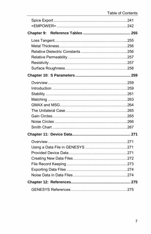
Table of Contents
7
Spice Export ...................................................................241=EMPOWER= ................................................................242
Chapter 9: Reference Tables ........................................... 255
Loss Tangent..................................................................255Metal Thickness..............................................................256Relative Dielectric Constants ..........................................256Relative Permeability ......................................................257Resistivity .......................................................................257Surface Roughness ........................................................258
Chapter 10: S Parameters .................................................. 259
Overview ........................................................................259Introduction ....................................................................259Stability ..........................................................................261Matching ........................................................................263GMAX and MSG.............................................................264The Unilateral Case........................................................265Gain Circles....................................................................265Noise Circles ..................................................................266Smith Chart ....................................................................267
Chapter 11: Device Data ..................................................... 271
Overview ........................................................................271Using a Data File in GENESYS ......................................271Provided Device Data.....................................................271Creating New Data Files .................................................272File Record Keeping .......................................................273Exporting Data Files .......................................................274Noise Data in Data Files .................................................274
Chapter 12: References ...................................................... 275
GENESYS References ...................................................275

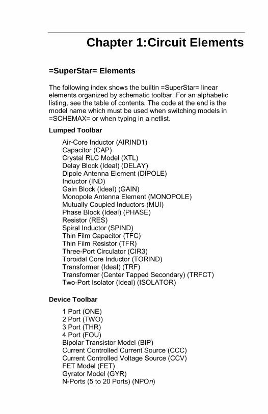
Chapter 1: Circuit Elements
=SuperStar= Elements
The following index shows the builtin =SuperStar= linearelements organized by schematic toolbar. For an alphabeticlisting, see the table of contents. The code at the end is themodel name which must be used when switching models in=SCHEMAX= or when typing in a netlist.
Lumped Toolbar
Air-Core Inductor (AIRIND1)Capacitor (CAP)Crystal RLC Model (XTL)Delay Block (Ideal) (DELAY)Dipole Antenna Element (DIPOLE)Inductor (IND)Gain Block (Ideal) (GAIN)Monopole Antenna Element (MONOPOLE)Mutually Coupled Inductors (MUI)Phase Block (Ideal) (PHASE)Resistor (RES)Spiral Inductor (SPIND)Thin Film Capacitor (TFC)Thin Film Resistor (TFR)Three-Port Circulator (CIR3)Toroidal Core Inductor (TORIND)Transformer (Ideal) (TRF)Transformer (Center Tapped Secondary) (TRFCT)Two-Port Isolator (Ideal) (ISOLATOR)
Device Toolbar
1 Port (ONE)2 Port (TWO)3 Port (THR)4 Port (FOU)Bipolar Transistor Model (BIP)Current Controlled Current Source (CCC)Current Controlled Voltage Source (CCV)FET Model (FET)Gyrator Model (GYR)N-Ports (5 to 20 Ports) (NPOn)
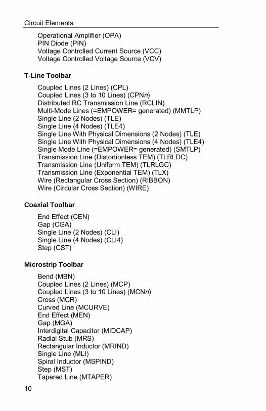
Circuit Elements
10
Operational Amplifier (OPA)PIN Diode (PIN)Voltage Controlled Current Source (VCC)Voltage Controlled Voltage Source (VCV)
T-Line Toolbar
Coupled Lines (2 Lines) (CPL)Coupled Lines (3 to 10 Lines) (CPNn)Distributed RC Transmission Line (RCLIN)Multi-Mode Lines (=EMPOWER= generated) (MMTLP)Single Line (2 Nodes) (TLE)Single Line (4 Nodes) (TLE4)Single Line With Physical Dimensions (2 Nodes) (TLE)Single Line With Physical Dimensions (4 Nodes) (TLE4)Single Mode Line (=EMPOWER= generated) (SMTLP)Transmission Line (Distortionless TEM) (TLRLDC)Transmission Line (Uniform TEM) (TLRLGC)Transmission Line (Exponential TEM) (TLX)Wire (Rectangular Cross Section) (RIBBON)Wire (Circular Cross Section) (WIRE)
Coaxial Toolbar
End Effect (CEN)Gap (CGA)Single Line (2 Nodes) (CLI)Single Line (4 Nodes) (CLI4)Step (CST)
Microstrip Toolbar
Bend (MBN)Coupled Lines (2 Lines) (MCP)Coupled Lines (3 to 10 Lines) (MCNn)Cross (MCR)Curved Line (MCURVE)End Effect (MEN)Gap (MGA)Interdigital Capacitor (MIDCAP)Radial Stub (MRS)Rectangular Inductor (MRIND)Single Line (MLI)Spiral Inductor (MSPIND)Step (MST)Tapered Line (MTAPER)
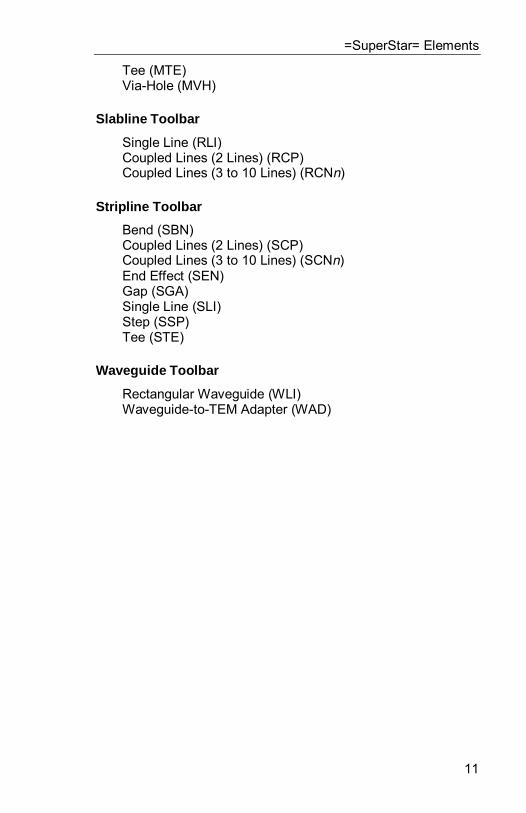
=SuperStar= Elements
11
Tee (MTE)Via-Hole (MVH)
Slabline Toolbar
Single Line (RLI)Coupled Lines (2 Lines) (RCP)Coupled Lines (3 to 10 Lines) (RCNn)
Stripline Toolbar
Bend (SBN)Coupled Lines (2 Lines) (SCP)Coupled Lines (3 to 10 Lines) (SCNn)End Effect (SEN)Gap (SGA)Single Line (SLI)Step (SSP)Tee (STE)
Waveguide Toolbar
Rectangular Waveguide (WLI)Waveguide-to-TEM Adapter (WAD)
Circuit Elements
12
ABCD parameters (ABC)
There is no symbol for this element in =SCHEMAX=. To createit, you must change the model for another symbol.
Netlist Syntax :
ABC 1 2 0 AR=-.5 AI=.5 BR=1 BI=-.2 CR=.1 CI=.3 DR=.5& DI=-.6
Parameters:
n1 Input node number.n2 Output node number.n3 Ground reference node number.AR Real portion of A.AI Imaginary portion of A.BR Real portion of B.BI Imaginary portion of B.CR Real portion of C.CI Imaginary portion of C.DR Real portion of D.DI Imaginary portion of D.
Example:
ABC 1 2 0 AR=-.5 AI=.5 BR=1 BI=-.2 CR=.1 CI=.3& DR=.5 DI=-.6

Air core inductor (AIRIND1)
13
Air core inductor (AIRIND1)
This symbol is available in =SCHEMAX= in the LUMPED toolbar.
Netlist syntax:
AIRIND1 n1 n2 N= D= L= WD= RHO= [Name=]
Parameters:
N Number of turnsD Diameter of form (mm)L Length (mm)WD Diameter of wire (mm)RHO Resistivity of conductor relative to copper
Examples:
AIRIND1 1 2 N=7 D=5.08 L=11.43 WD=1.143 RHO=1
Touchstone Translation:
AIRIND1 1 2 N= D= L= WD= RHO=
Default SPICE Translation:
None
Circuit Elements
14
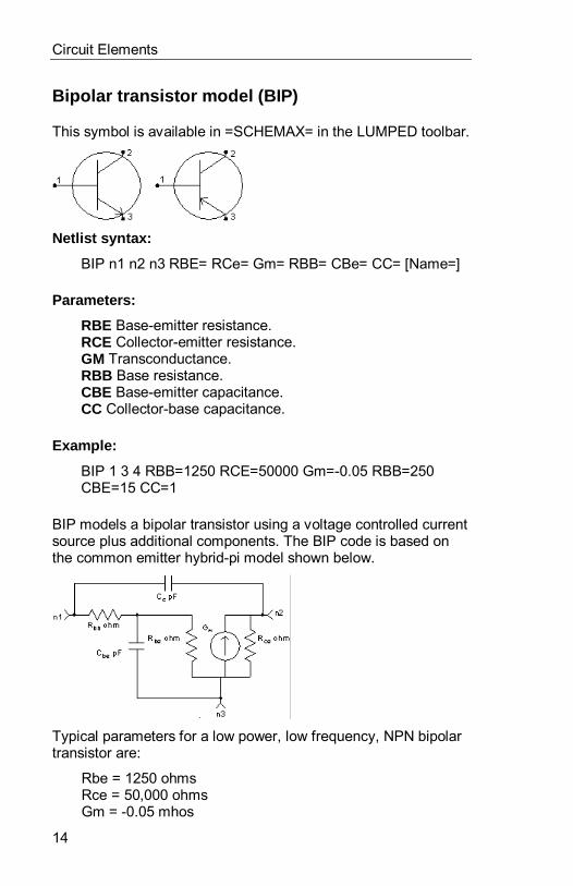
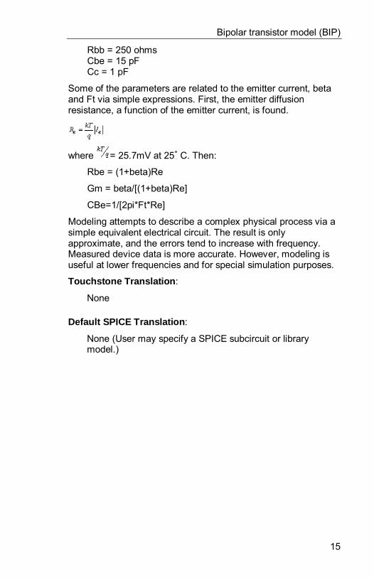
Bipolar transistor model (BIP)
This symbol is available in =SCHEMAX= in the LUMPED toolbar.
Netlist syntax:
BIP n1 n2 n3 RBE= RCe= Gm= RBB= CBe= CC= [Name=]
Parameters:
RBE Base-emitter resistance.RCE Collector-emitter resistance.GM Transconductance.RBB Base resistance.CBE Base-emitter capacitance.CC Collector-base capacitance.
Example:
BIP 1 3 4 RBB=1250 RCE=50000 Gm=-0.05 RBB=250CBE=15 CC=1
BIP models a bipolar transistor using a voltage controlled currentsource plus additional components. The BIP code is based onthe common emitter hybrid-pi model shown below.
Typical parameters for a low power, low frequency, NPN bipolartransistor are:
Rbe = 1250 ohmsRce = 50,000 ohmsGm = -0.05 mhos
Bipolar transistor model (BIP)
15
Rbb = 250 ohmsCbe = 15 pFCc = 1 pF
Some of the parameters are related to the emitter current, betaand Ft via simple expressions. First, the emitter diffusionresistance, a function of the emitter current, is found.
where = 25.7mV at 25 C. Then:
Rbe = (1+beta)Re
Gm = beta/[(1+beta)Re]
CBe=1/[2pi*Ft*Re]
Modeling attempts to describe a complex physical process via asimple equivalent electrical circuit. The result is onlyapproximate, and the errors tend to increase with frequency.Measured device data is more accurate. However, modeling isuseful at lower frequencies and for special simulation purposes.
Touchstone Translation :
None
Default SPICE Translation :
None (User may specify a SPICE subcircuit or librarymodel.)
Circuit Elements
16
Capacitor (CAP)
Lumped capacitance with optional Q. This symbol is available in=SCHEMAX= in the LUMPED toolbar.
Netlist syntax:
CAP n1 n2 C= [Q=] [Name=]
Parameters:
Capacitance (pF) Specifies the value of the capacitor inpicoFarads.Capacitor Q (optional) Specifies the quality factor of thecapacitor, modeled as constant with frequency. Thisparameter is not required, and defaults to 1 million if notspecified.
Examples:
CAP 1 2 C=22CAP 3 0 C=470 Q=300 N=C1
Q is modeled as constant with frequency. It can be specifiedhigher or lower than the default value.
Touchstone Translation:
CAP n1 n2 C=or (if Q is specified)
CAPQ n1 n2 C= Q= F=1 MOD=3
Default SPICE Translation:
C1_NAME n1 n2 CWarning: Q is not modeled in SPICE.
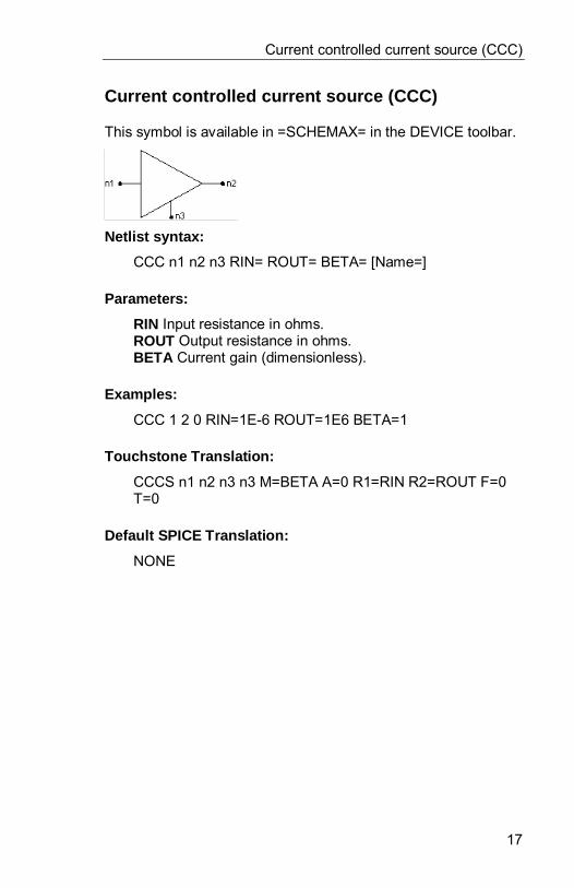
Current controlled current source (CCC)
17
Current controlled current source (CCC)
This symbol is available in =SCHEMAX= in the DEVICE toolbar.
Netlist syntax:
CCC n1 n2 n3 RIN= ROUT= BETA= [Name=]
Parameters:
RIN Input resistance in ohms.ROUT Output resistance in ohms.BETA Current gain (dimensionless).
Examples:
CCC 1 2 0 RIN=1E-6 ROUT=1E6 BETA=1
Touchstone Translation:
CCCS n1 n2 n3 n3 M=BETA A=0 R1=RIN R2=ROUT F=0T=0
Default SPICE Translation:
NONE
Circuit Elements
18
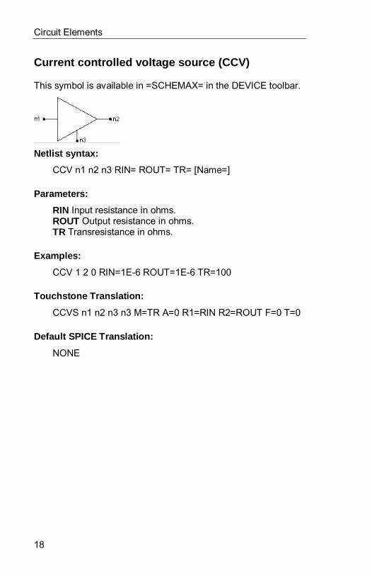
Current controlled voltage source (CCV)
This symbol is available in =SCHEMAX= in the DEVICE toolbar.
Netlist syntax:
CCV n1 n2 n3 RIN= ROUT= TR= [Name=]
Parameters:
RIN Input resistance in ohms.ROUT Output resistance in ohms.TR Transresistance in ohms.
Examples:
CCV 1 2 0 RIN=1E-6 ROUT=1E-6 TR=100
Touchstone Translation:
CCVS n1 n2 n3 n3 M=TR A=0 R1=RIN R2=ROUT F=0 T=0
Default SPICE Translation:
NONE
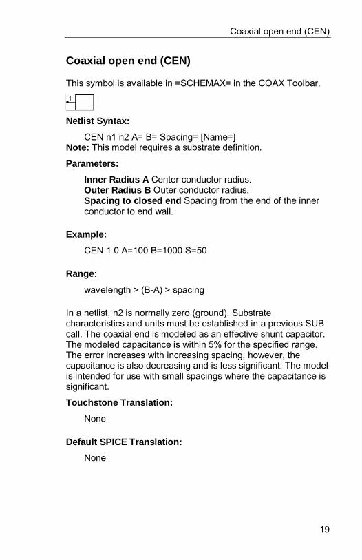
Coaxial open end (CEN)
19
Coaxial open end (CEN)
This symbol is available in =SCHEMAX= in the COAX Toolbar.
Netlist Syntax:
CEN n1 n2 A= B= Spacing= [Name=]Note: This model requires a substrate definition.
Parameters:
Inner Radius A Center conductor radius.Outer Radius B Outer conductor radius.Spacing to closed end Spacing from the end of the innerconductor to end wall.
Example:
CEN 1 0 A=100 B=1000 S=50
Range:
wavelength > (B-A) > spacing
In a netlist, n2 is normally zero (ground). Substratecharacteristics and units must be established in a previous SUBcall. The coaxial end is modeled as an effective shunt capacitor.The modeled capacitance is within 5% for the specified range.The error increases with increasing spacing, however, thecapacitance is also decreasing and is less significant. The modelis intended for use with small spacings where the capacitance issignificant.
Touchstone Translation:
None
Default SPICE Translation:
None
Circuit Elements
20
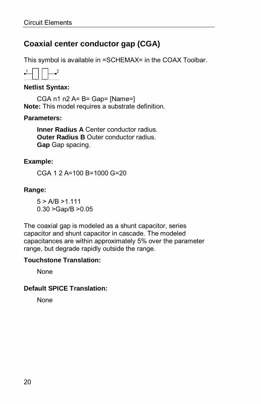
Coaxial center conductor gap (CGA)
This symbol is available in =SCHEMAX= in the COAX Toolbar.
Netlist Syntax:
CGA n1 n2 A= B= Gap= [Name=]Note: This model requires a substrate definition.
Parameters:
Inner Radius A Center conductor radius.Outer Radius B Outer conductor radius.Gap Gap spacing.
Example:
CGA 1 2 A=100 B=1000 G=20
Range:
5 > A/B >1.1110.30 >Gap/B >0.05
The coaxial gap is modeled as a shunt capacitor, seriescapacitor and shunt capacitor in cascade. The modeledcapacitances are within approximately 5% over the parameterrange, but degrade rapidly outside the range.
Touchstone Translation:
None
Default SPICE Translation:
None
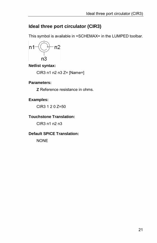
Ideal three port circulator (CIR3)
21
Ideal three port circulator (CIR3)
This symbol is available in =SCHEMAX= in the LUMPED toolbar.
Netlist syntax:
CIR3 n1 n2 n3 Z= [Name=]
Parameters:
Z Reference resistance in ohms.
Examples:
CIR3 1 2 0 Z=50
Touchstone Translation:
CIR3 n1 n2 n3
Default SPICE Translation:
NONE
Circuit Elements
22
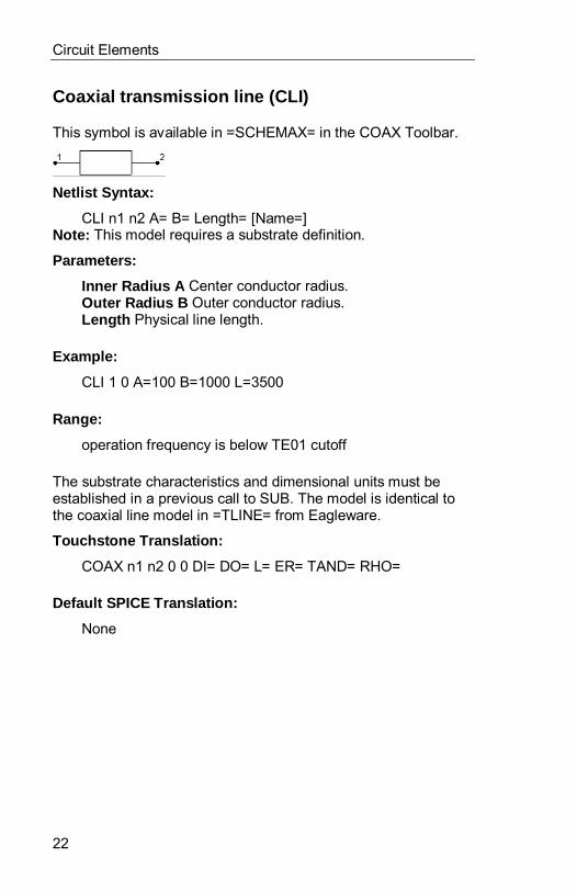
Coaxial transmission line (CLI)
This symbol is available in =SCHEMAX= in the COAX Toolbar.
Netlist Syntax:
CLI n1 n2 A= B= Length= [Name=]Note: This model requires a substrate definition.
Parameters:
Inner Radius A Center conductor radius.Outer Radius B Outer conductor radius.Length Physical line length.
Example:
CLI 1 0 A=100 B=1000 L=3500
Range:
operation frequency is below TE01 cutoff
The substrate characteristics and dimensional units must beestablished in a previous call to SUB. The model is identical tothe coaxial line model in =TLINE= from Eagleware.
Touchstone Translation:
COAX n1 n2 0 0 DI= DO= L= ER= TAND= RHO=
Default SPICE Translation:
None
Four terminal coaxial line (CLI4)
23
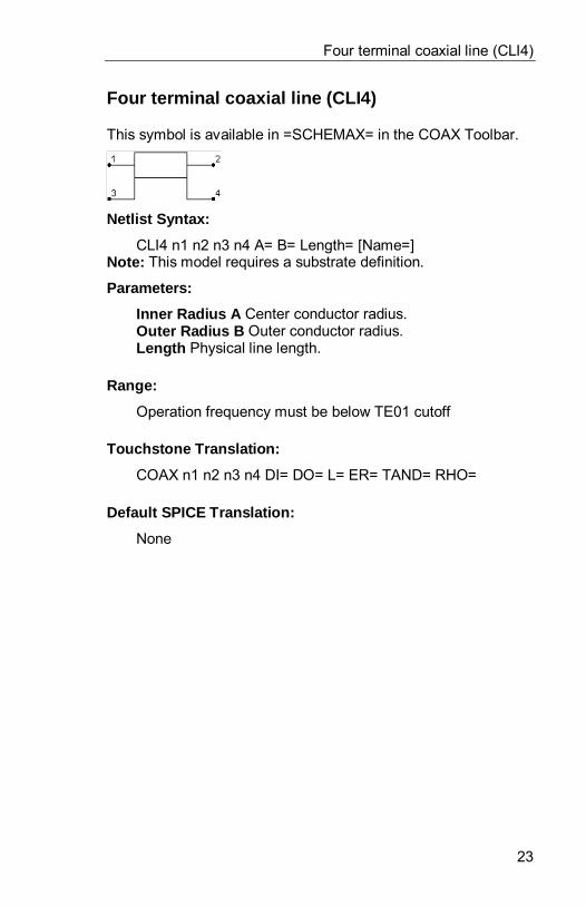
Four terminal coaxial line (CLI4)
This symbol is available in =SCHEMAX= in the COAX Toolbar.
Netlist Syntax:
CLI4 n1 n2 n3 n4 A= B= Length= [Name=]Note: This model requires a substrate definition.
Parameters:
Inner Radius A Center conductor radius.Outer Radius B Outer conductor radius.Length Physical line length.
Range:
Operation frequency must be below TE01 cutoff
Touchstone Translation:
COAX n1 n2 n3 n4 DI= DO= L= ER= TAND= RHO=
Default SPICE Translation:
None
Circuit Elements
24
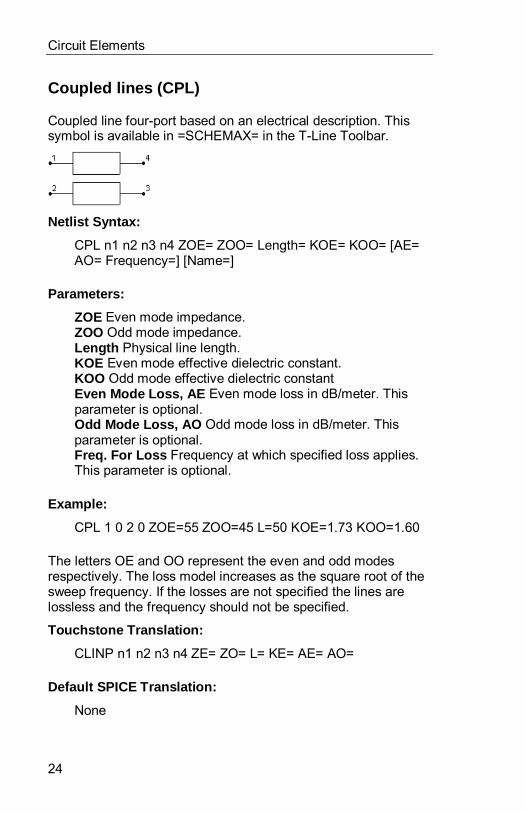
Coupled lines (CPL)
Coupled line four-port based on an electrical description. Thissymbol is available in =SCHEMAX= in the T-Line Toolbar.
Netlist Syntax:
CPL n1 n2 n3 n4 ZOE= ZOO= Length= KOE= KOO= [AE=AO= Frequency=] [Name=]
Parameters:
ZOE Even mode impedance.ZOO Odd mode impedance.Length Physical line length.KOE Even mode effective dielectric constant.KOO Odd mode effective dielectric constantEven Mode Loss, AE Even mode loss in dB/meter. Thisparameter is optional.Odd Mode Loss, AO Odd mode loss in dB/meter. Thisparameter is optional.Freq. For Loss Frequency at which specified loss applies.This parameter is optional.
Example:
CPL 1 0 2 0 ZOE=55 ZOO=45 L=50 KOE=1.73 KOO=1.60
The letters OE and OO represent the even and odd modesrespectively. The loss model increases as the square root of thesweep frequency. If the losses are not specified the lines arelossless and the frequency should not be specified.
Touchstone Translation:
CLINP n1 n2 n3 n4 ZE= ZO= L= KE= AE= AO=
Default SPICE Translation:
None
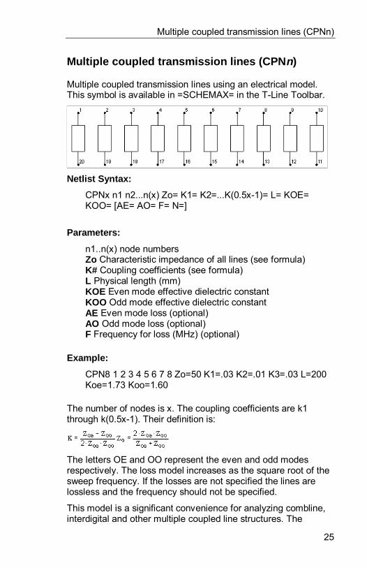
Multiple coupled transmission lines (CPNn)
25
Multiple coupled transmission lines (CPN n)
Multiple coupled transmission lines using an electrical model.This symbol is available in =SCHEMAX= in the T-Line Toolbar.
Netlist Syntax:
CPNx n1 n2...n(x) Zo= K1= K2=...K(0.5x-1)= L= KOE=KOO= [AE= AO= F= N=]
Parameters:
n1..n(x) node numbersZo Characteristic impedance of all lines (see formula)K# Coupling coefficients (see formula)L Physical length (mm)KOE Even mode effective dielectric constantKOO Odd mode effective dielectric constantAE Even mode loss (optional)AO Odd mode loss (optional)F Frequency for loss (MHz) (optional)
Example:
CPN8 1 2 3 4 5 6 7 8 Zo=50 K1=.03 K2=.01 K3=.03 L=200Koe=1.73 Koo=1.60
The number of nodes is x. The coupling coefficients are k1through k(0.5x-1). Their definition is:
The letters OE and OO represent the even and odd modesrespectively. The loss model increases as the square root of thesweep frequency. If the losses are not specified the lines arelossless and the frequency should not be specified.
This model is a significant convenience for analyzing combline,interdigital and other multiple coupled line structures. The

Circuit Elements
26
multiple coupled line model is based on an exact wire-lineequivalent of cascaded coupled pairs of lines (CPL).
Touchstone Translation:
None
Default SPICE Translation:
None
Coaxial conductor step (CST)
27
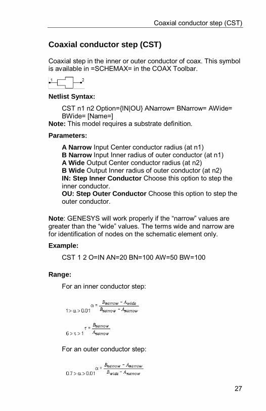
Coaxial conductor step (CST)
Coaxial step in the inner or outer conductor of coax. This symbolis available in =SCHEMAX= in the COAX Toolbar.
Netlist Syntax:
CST n1 n2 Option={IN|OU} ANarrow= BNarrow= AWide=BWide= [Name=]
Note: This model requires a substrate definition.
Parameters:
A Narrow Input Center conductor radius (at n1)B Narrow Input Inner radius of outer conductor (at n1)A Wide Output Center conductor radius (at n2)B Wide Output Inner radius of outer conductor (at n2)IN: Step Inner Conductor Choose this option to step theinner conductor.OU: Step Outer Conductor Choose this option to step theouter conductor.
Note : GENESYS will work properly if the “narrow” values aregreater than the “wide” values. The terms wide and narrow arefor identification of nodes on the schematic element only.
Example:
CST 1 2 O=IN AN=20 BN=100 AW=50 BW=100
Range:
For an inner conductor step:
For an outer conductor step:

Circuit Elements
28
Option IN indicates a step in the inner conductor and OUindicates a step in the outer conductor. The dielectric andconductor characteristics and dimensional units must beestablished in a previous call to SUB. A step in both conductorsis modeled by cascading two steps.
The coaxial step is modeled as an effective shunt capacitor. Themodeled effective capacitance is within approximately 0.2pF/BNarrow (meters) for inner conductor steps and 0.4pF/BNarrow (meters) for outer conductor steps.
Touchstone Translation:
None
Default SPICE Translation:
None
Ideal delay block (DELAY)
29
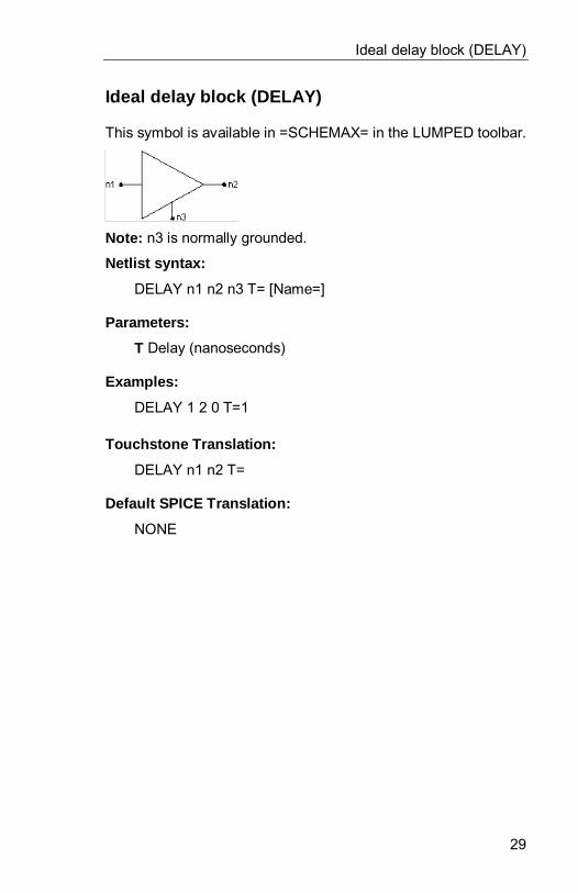
Ideal delay block (DELAY)
This symbol is available in =SCHEMAX= in the LUMPED toolbar.
Note: n3 is normally grounded.
Netlist syntax:
DELAY n1 n2 n3 T= [Name=]
Parameters:
T Delay (nanoseconds)
Examples:
DELAY 1 2 0 T=1
Touchstone Translation:
DELAY n1 n2 T=
Default SPICE Translation:
NONE
Circuit Elements
30
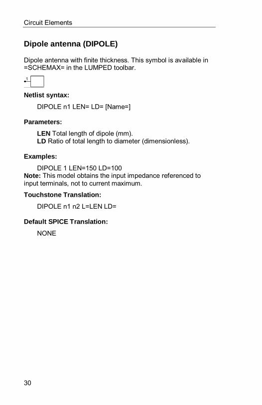
Dipole antenna (DIPOLE)
Dipole antenna with finite thickness. This symbol is available in=SCHEMAX= in the LUMPED toolbar.
Netlist syntax:
DIPOLE n1 LEN= LD= [Name=]
Parameters:
LEN Total length of dipole (mm).LD Ratio of total length to diameter (dimensionless).
Examples:
DIPOLE 1 LEN=150 LD=100Note: This model obtains the input impedance referenced toinput terminals, not to current maximum.
Touchstone Translation:
DIPOLE n1 n2 L=LEN LD=
Default SPICE Translation:
NONE
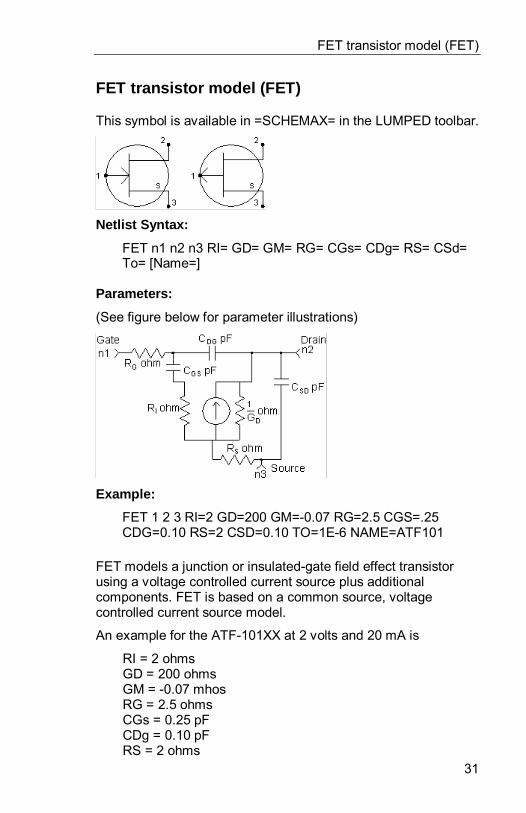
FET transistor model (FET)
31
FET transistor model (FET)
This symbol is available in =SCHEMAX= in the LUMPED toolbar.
Netlist Syntax:
FET n1 n2 n3 RI= GD= GM= RG= CGs= CDg= RS= CSd=To= [Name=]
Parameters:
(See figure below for parameter illustrations)
Example:
FET 1 2 3 RI=2 GD=200 GM=-0.07 RG=2.5 CGS=.25CDG=0.10 RS=2 CSD=0.10 TO=1E-6 NAME=ATF101
FET models a junction or insulated-gate field effect transistorusing a voltage controlled current source plus additionalcomponents. FET is based on a common source, voltagecontrolled current source model.
An example for the ATF-101XX at 2 volts and 20 mA is
RI = 2 ohmsGD = 200 ohmsGM = -0.07 mhosRG = 2.5 ohmsCGs = 0.25 pFCDg = 0.10 pFRS = 2 ohms
Circuit Elements
32
CSd = 0.10 pFTo = 1E-6 nanoseconds
The Wolf and Avantek models place the drain-sourcecapacitance in slightly different positions. Also, the Avantekmodel includes information on chip and bond-wire inductances.The Wolf model includes a shunt R-L network at the input. Incritical applications, these differences are readily incorporated in=SuperStar= by externally adding the appropriate components tothe FET model.
Modeling describes a complex physical process via a simpleequivalent electrical circuit. The result is approximate, and theerror tends to increase with frequency. Measured device data ismore accurate. Models are best for lower frequencies andspecial purposes.
Equations which reduce the model to exact equivalent Y or otherparameters for use in a simulation program are quite complex.Authors (including Wolf in his derivation of Y-parameters) oftenmake simplifying assumptions to the equations. This is not thecase in =SuperStar=, where the program exactly matches themodel schematic. Therefore, you may experience smalldifferences in the response computed by =SuperStar= and othersimulation programs. The differences are generally insignificantin relation to errors associated with the modeling process.
Touchstone Translation:
None
Default SPICE Translation:
.SUBCKT X$NAME 1 2 3R_g 1 4 rgC_dg 4 2 cdg pFC_Gs 4 5 cgs pFR_i 5 6 riR_s 3 6 rsR_d 2 6 rd pFC_sd 2 3 csd pFG_Gm 6 2 5 6 Gm.ENDS X$NAME
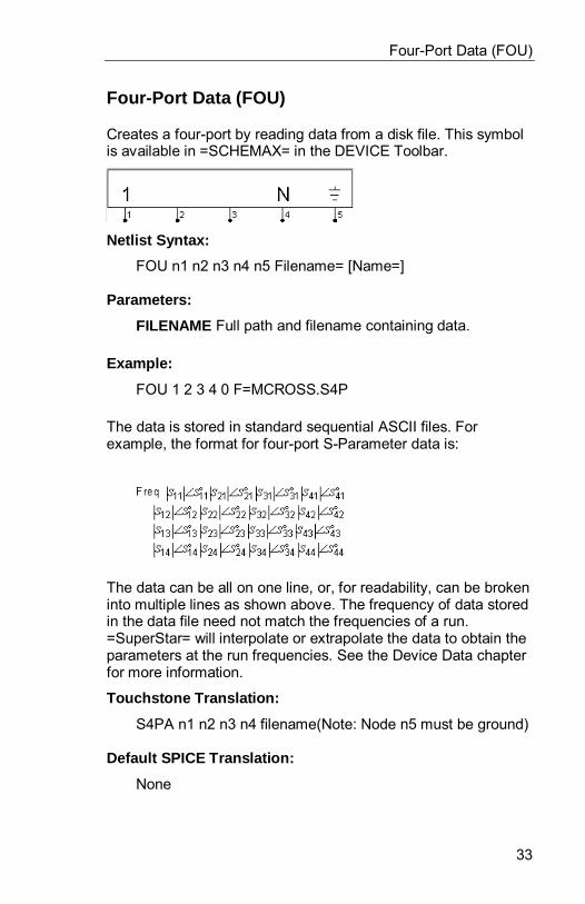
Four-Port Data (FOU)
33
Four-Port Data (FOU)
Creates a four-port by reading data from a disk file. This symbolis available in =SCHEMAX= in the DEVICE Toolbar.
Netlist Syntax:
FOU n1 n2 n3 n4 n5 Filename= [Name=]
Parameters:
FILENAME Full path and filename containing data.
Example:
FOU 1 2 3 4 0 F=MCROSS.S4P
The data is stored in standard sequential ASCII files. Forexample, the format for four-port S-Parameter data is:
The data can be all on one line, or, for readability, can be brokeninto multiple lines as shown above. The frequency of data storedin the data file need not match the frequencies of a run.=SuperStar= will interpolate or extrapolate the data to obtain theparameters at the run frequencies. See the Device Data chapterfor more information.
Touchstone Translation:
S4PA n1 n2 n3 n4 filename(Note: Node n5 must be ground)
Default SPICE Translation:
None
Circuit Elements
34
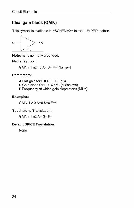
Ideal gain block (GAIN)
This symbol is available in =SCHEMAX= in the LUMPED toolbar.
Note: n3 is normally grounded.
Netlist syntax:
GAIN n1 n2 n3 A= S= F= [Name=]
Parameters:
A Flat gain for 0<FREQ<F (dB)S Gain slope for FREQ>=F (dB/octave)F Frequency at which gain slope starts (MHz).
Examples:
GAIN 1 2 0 A=6 S=6 F=4
Touchstone Translation:
GAIN n1 n2 A= S= F=
Default SPICE Translation:
None
Gyrator (GYR)
35
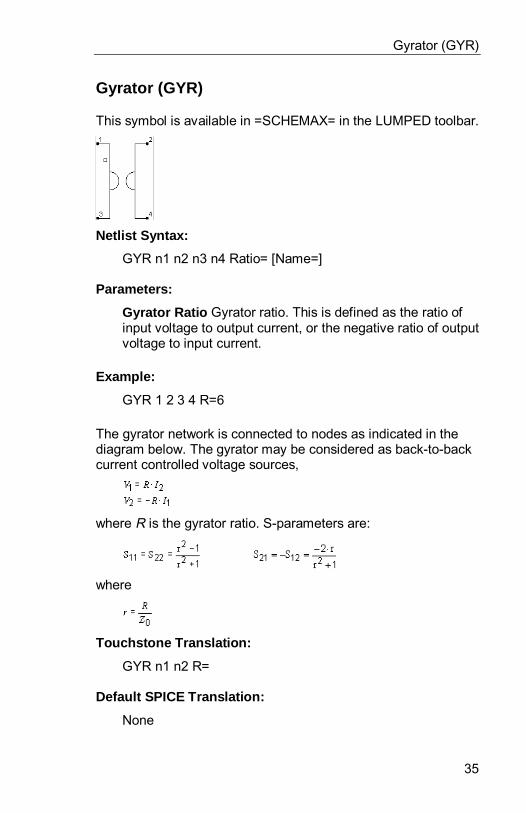
Gyrator (GYR)
This symbol is available in =SCHEMAX= in the LUMPED toolbar.
Netlist Syntax:
GYR n1 n2 n3 n4 Ratio= [Name=]
Parameters:
Gyrator Ratio Gyrator ratio. This is defined as the ratio ofinput voltage to output current, or the negative ratio of outputvoltage to input current.
Example:
GYR 1 2 3 4 R=6
The gyrator network is connected to nodes as indicated in thediagram below. The gyrator may be considered as back-to-backcurrent controlled voltage sources,
where R is the gyrator ratio. S-parameters are:
where
Touchstone Translation:
GYR n1 n2 R=
Default SPICE Translation:
None
Circuit Elements
36
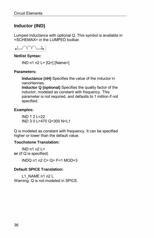
Inductor (IND)
Lumped inductance with optional Q. This symbol is available in=SCHEMAX= in the LUMPED toolbar.
Netlist Syntax:
IND n1 n2 L= [Q=] [Name=]
Parameters:
Inductance (nH) Specifies the value of the inductor innanoHenries.Inductor Q (optional) Specifies the quality factor of theinductor, modeled as constant with frequency. Thisparameter is not required, and defaults to 1 million if notspecified.
Examples:
IND 1 2 L=22IND 3 0 L=470 Q=300 N=L1
Q is modeled as constant with frequency. It can be specifiedhigher or lower than the default value.
Touchstone Translation:
IND n1 n2 L=or (if Q is specified)
INDQ n1 n2 C= Q= F=1 MOD=3
Default SPICE Translation:
L1_NAME n1 n2 LWarning: Q is not modeled in SPICE.
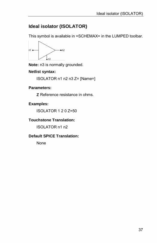
Ideal isolator (ISOLATOR)
37
Ideal isolator (ISOLATOR)
This symbol is available in =SCHEMAX= in the LUMPED toolbar.
Note: n3 is normally grounded.
Netlist syntax:
ISOLATOR n1 n2 n3 Z= [Name=]
Parameters:
Z Reference resistance in ohms.
Examples:
ISOLATOR 1 2 0 Z=50
Touchstone Translation:
ISOLATOR n1 n2
Default SPICE Translation:
None
Circuit Elements
38
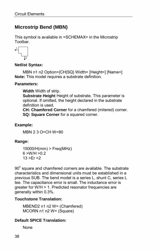
Microstrip Bend (MBN)
This symbol is available in =SCHEMAX= in the MicrostripToolbar.
Netlist Syntax:
MBN n1 n2 Option={CH|SQ} Width= [Height=] [Name=]Note: This model requires a substrate definition.
Parameters:
Width Width of strip.Substrate Height Height of substrate. This parameter isoptional. If omitted, the height declared in the substratedefinition is used.CH: Chamfered Corner for a chamfered (mitered) corner.SQ: Square Corner for a squared corner.
Example:
MBN 2 3 O=CH W=80
Range:
15000/H(mm) > Freq(MHz)6 >W/H >0.213 >Er >2
90o square and chamfered corners are available. The substratecharacteristics and dimensional units must be established in aprevious SUB. The bend model is a series L, shunt C, series Ltee. The capacitance error is small. The inductance error isgreater for W/H > 1. Predicted resonator frequencies aregenerally within 0.3%.
Touchstone Translation:
MBEND2 n1 n2 W= (Chamfered)MCORN n1 n2 W= (Square)
Default SPICE Translation:
None
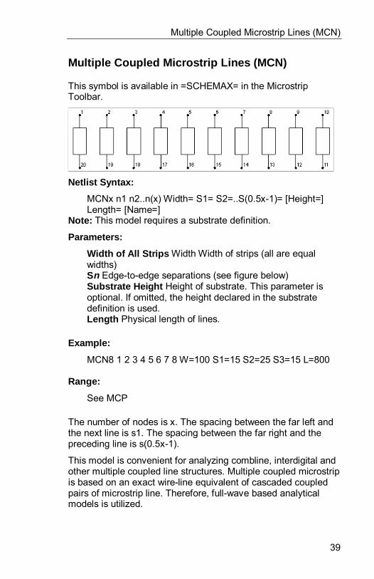
Multiple Coupled Microstrip Lines (MCN)
39
Multiple Coupled Microstrip Lines (MCN)
This symbol is available in =SCHEMAX= in the MicrostripToolbar.
Netlist Syntax:
MCNx n1 n2..n(x) Width= S1= S2=..S(0.5x-1)= [Height=]Length= [Name=]
Note: This model requires a substrate definition.
Parameters:
Width of All Strips Width Width of strips (all are equalwidths)Sn Edge-to-edge separations (see figure below)Substrate Height Height of substrate. This parameter isoptional. If omitted, the height declared in the substratedefinition is used.Length Physical length of lines.
Example:
MCN8 1 2 3 4 5 6 7 8 W=100 S1=15 S2=25 S3=15 L=800
Range:
See MCP
The number of nodes is x. The spacing between the far left andthe next line is s1. The spacing between the far right and thepreceding line is s(0.5x-1).
This model is convenient for analyzing combline, interdigital andother multiple coupled line structures. Multiple coupled microstripis based on an exact wire-line equivalent of cascaded coupledpairs of microstrip line. Therefore, full-wave based analyticalmodels is utilized.

Circuit Elements
40
Touchstone Translation:
(Translation is only available for MCN6)MACLIN3 n1 n2 n3 n4 n5 n6 W1= W2= W3= S1= S2= L=
Default SPICE Translation:
None
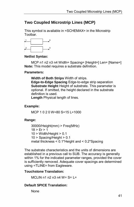
Two Coupled Microstrip Lines (MCP)
41
Two Coupled Microstrip Lines (MCP)
This symbol is available in =SCHEMAX= in the MicrostripToolbar.
Netlist Syntax:
MCP n1 n2 n3 n4 Width= Spacing= [Height=] Len= [Name=]Note: This model requires a substrate definition.
Parameters:
Width of Both Strips Width of strips.Edge-to-Edge Spacing Edge-to-edge strip separationSubstrate Height Height of substrate. This parameter isoptional. If omitted, the height declared in the substratedefinition is used.Length Physical length of lines.
Example:
MCP 1 0 2 0 W=80 S=15 L=1000
Range:
30000/Height(mm) > Freq(MHz)18 > Er > 110 > Width/Height > 0.110 > Spacing/Height > 0.1metal thickness < 0.1*Height and < 0.2*Spacing
The substrate characteristics and the units of dimensions areestablished in a previous call to SUB. The accuracy is generallywithin 1% for the indicated parameter ranges, provided the coveris sufficiently removed. Adequate cover spacings are determinedusing =TLINE= from Eagleware.
Touchstone Translation:
MCLIN n1 n2 n3 n4 W= S= L=
Default SPICE Translation:
None
Circuit Elements
42
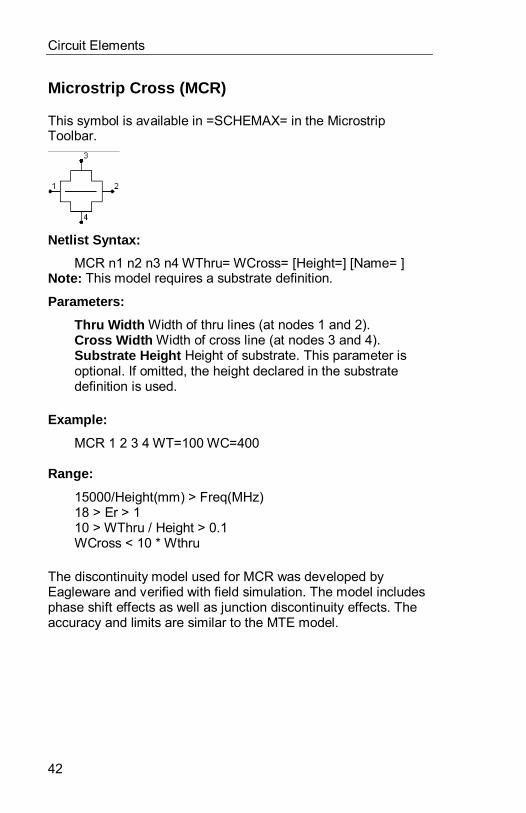
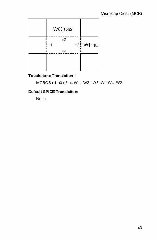
Microstrip Cross (MCR)
This symbol is available in =SCHEMAX= in the MicrostripToolbar.
Netlist Syntax:
MCR n1 n2 n3 n4 WThru= WCross= [Height=] [Name= ]Note: This model requires a substrate definition.
Parameters:
Thru Width Width of thru lines (at nodes 1 and 2).Cross Width Width of cross line (at nodes 3 and 4).Substrate Height Height of substrate. This parameter isoptional. If omitted, the height declared in the substratedefinition is used.
Example:
MCR 1 2 3 4 WT=100 WC=400
Range:
15000/Height(mm) > Freq(MHz)18 > Er > 110 > WThru / Height > 0.1WCross < 10 * Wthru
The discontinuity model used for MCR was developed byEagleware and verified with field simulation. The model includesphase shift effects as well as junction discontinuity effects. Theaccuracy and limits are similar to the MTE model.
Microstrip Cross (MCR)
43
Touchstone Translation:
MCROS n1 n3 n2 n4 W1= W2= W3=W1 W4=W2
Default SPICE Translation:
None

Circuit Elements
44
Microstrip Curved Bend (MCURVE)
This symbol is available in =SCHEMAX= in the MicrostripToolbar.
Netlist syntax:
MCURVE n1 n2 W= ANG= RAD= [Name=]Note: This model requires a substrate definition.
Parameters:
(See figure below for an illustration of parameters).W Width of microstrip line.ANG Angle of bend in degrees.RAD Radius of bend measured to center of line.
Examples:
MCURVE 1 2 W=25 ANG=90 RAD=50
Touchstone Translation:
MCURVE n1 n2 W= ANG= RAD=
Default SPICE Translation:
None
Microstrip Open End (MEN)
45
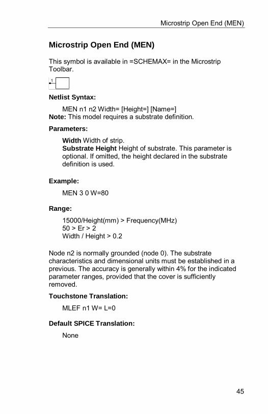
Microstrip Open End (MEN)
This symbol is available in =SCHEMAX= in the MicrostripToolbar.
Netlist Syntax:
MEN n1 n2 Width= [Height=] [Name=]Note: This model requires a substrate definition.
Parameters:
Width Width of strip.Substrate Height Height of substrate. This parameter isoptional. If omitted, the height declared in the substratedefinition is used.
Example:
MEN 3 0 W=80
Range:
15000/Height(mm) > Frequency(MHz)50 > Er > 2Width / Height > 0.2
Node n2 is normally grounded (node 0). The substratecharacteristics and dimensional units must be established in aprevious. The accuracy is generally within 4% for the indicatedparameter ranges, provided that the cover is sufficientlyremoved.
Touchstone Translation:
MLEF n1 W= L=0
Default SPICE Translation:
None
Circuit Elements
46
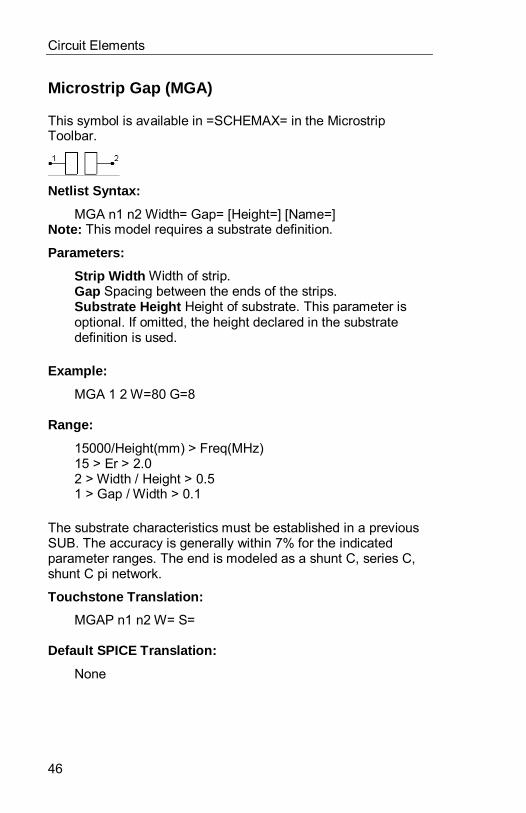
Microstrip Gap (MGA)
This symbol is available in =SCHEMAX= in the MicrostripToolbar.
Netlist Syntax:
MGA n1 n2 Width= Gap= [Height=] [Name=]Note: This model requires a substrate definition.
Parameters:
Strip Width Width of strip.Gap Spacing between the ends of the strips.Substrate Height Height of substrate. This parameter isoptional. If omitted, the height declared in the substratedefinition is used.
Example:
MGA 1 2 W=80 G=8
Range:
15000/Height(mm) > Freq(MHz)15 > Er > 2.02 > Width / Height > 0.51 > Gap / Width > 0.1
The substrate characteristics must be established in a previousSUB. The accuracy is generally within 7% for the indicatedparameter ranges. The end is modeled as a shunt C, series C,shunt C pi network.
Touchstone Translation:
MGAP n1 n2 W= S=
Default SPICE Translation:
None
Microstrip Interdigital Capacitor (MIDCAP)
47
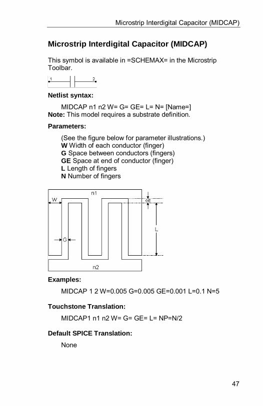
Microstrip Interdigital Capacitor (MIDCAP)
This symbol is available in =SCHEMAX= in the MicrostripToolbar.
Netlist syntax:
MIDCAP n1 n2 W= G= GE= L= N= [Name=]Note: This model requires a substrate definition.
Parameters:
(See the figure below for parameter illustrations.)W Width of each conductor (finger)G Space between conductors (fingers)GE Space at end of conductor (finger)L Length of fingersN Number of fingers
Examples:
MIDCAP 1 2 W=0.005 G=0.005 GE=0.001 L=0.1 N=5
Touchstone Translation:
MIDCAP1 n1 n2 W= G= GE= L= NP=N/2
Default SPICE Translation:
None
Circuit Elements
48
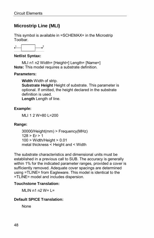
Microstrip Line (MLI)
This symbol is available in =SCHEMAX= in the MicrostripToolbar.
Netlist Syntax:
MLI n1 n2 Width= [Height=] Length= [Name=]Note: This model requires a substrate definition.
Parameters:
Width Width of strip.Substrate Height Height of substrate. This parameter isoptional. If omitted, the height declared in the substratedefinition is used.Length Length of line.
Example:
MLI 1 2 W=80 L=200
Range:
30000/Height(mm) > Frequency(MHz)128 > Er > 1100 > Width/Height > 0.01metal thickness < Height and < Width
The substrate characteristics and dimensional units must beestablished in a previous call to SUB. The accuracy is generallywithin 1% for the indicated parameter ranges, provided a cover issufficiently removed. Adequate cover spacings are determinedusing =TLINE= from Eagleware. This model is identical to the=TLINE= model and includes dispersion.
Touchstone Translation:
MLIN n1 n2 W= L=
Default SPICE Translation:
None
Monopole Antenna (MONOPOLE)
49
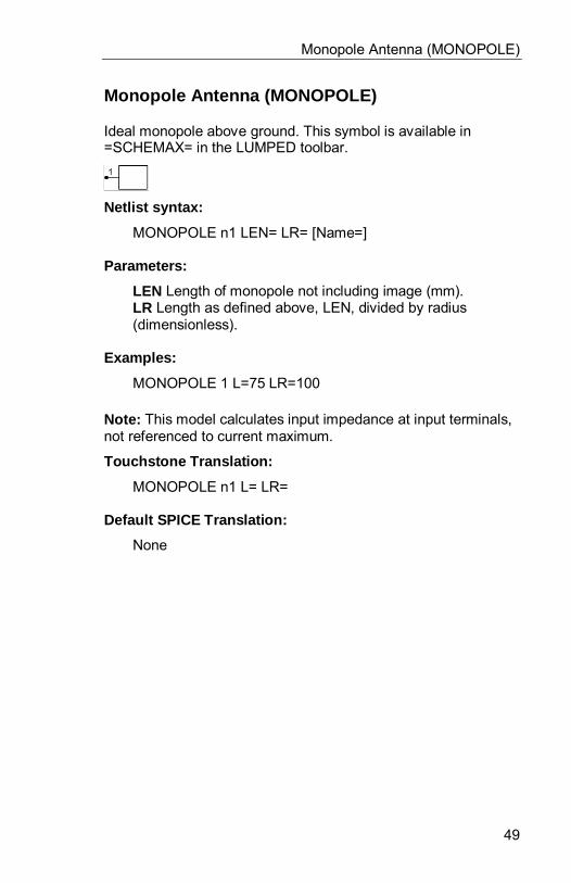
Monopole Antenna (MONOPOLE)
Ideal monopole above ground. This symbol is available in=SCHEMAX= in the LUMPED toolbar.
Netlist syntax:
MONOPOLE n1 LEN= LR= [Name=]
Parameters:
LEN Length of monopole not including image (mm).LR Length as defined above, LEN, divided by radius(dimensionless).
Examples:
MONOPOLE 1 L=75 LR=100
Note: This model calculates input impedance at input terminals,not referenced to current maximum.
Touchstone Translation:
MONOPOLE n1 L= LR=
Default SPICE Translation:
None

Circuit Elements
50
Microstrip Rectangular Inductor (MRIND)
This symbol is available in =SCHEMAX= in the MicrostripToolbar.
Netlist syntax:
MRIND 1 2 L1=20 L2=50 L3=50 W=5 S=5 N=7.16Note: This model requires a substrate definition.
Parameters:
(See figure below for parameter illustrations.)Length, 1st inside segment (L1) Length of the firstsegment from the inside tap pointLength, 2nd inside segment (L2) Length of the secondsegment from the inside tap pointLength, 3rd inside segment (L3) Length of the thirdsegment from the inside tap pointStrip Width (W) Width of conductor strips.Strip Spacing (S) Space between conductors.Number of Turns (n) Total number of turns. This does notneed to be an integer.
Examples:
MRIND 1 2 L1=0.715 L2=0.715 L3=.9 W=0.02 S=0.02 N=7

Microstrip Rectangular Inductor (MRIND)
51
Touchstone Translation:
MRIND n1 n2 N=N/4 L1= L2= W= S=
Default SPICE Translation:
None
Circuit Elements
52
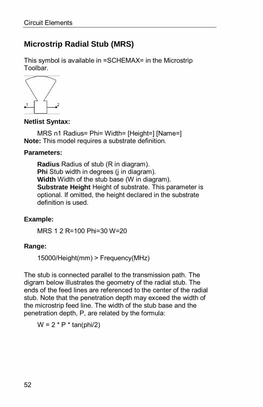
Microstrip Radial Stub (MRS)
This symbol is available in =SCHEMAX= in the MicrostripToolbar.
Netlist Syntax:
MRS n1 Radius= Phi= Width= [Height=] [Name=]Note: This model requires a substrate definition.
Parameters:
Radius Radius of stub (R in diagram).Phi Stub width in degrees (j in diagram).Width Width of the stub base (W in diagram).Substrate Height Height of substrate. This parameter isoptional. If omitted, the height declared in the substratedefinition is used.
Example:
MRS 1 2 R=100 Phi=30 W=20
Range:
15000/Height(mm) > Frequency(MHz)
The stub is connected parallel to the transmission path. Thedigram below illustrates the geometry of the radial stub. Theends of the feed lines are referenced to the center of the radialstub. Note that the penetration depth may exceed the width ofthe microstrip feed line. The width of the stub base and thepenetration depth, P, are related by the formula:
W = 2 * P * tan(phi/2)

Microstrip Radial Stub (MRS)
53
Touchstone Translation:
MRSTUB n1 WI= L= ANG=
Default SPICE Translation:
None
Circuit Elements
54
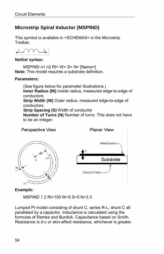
Microstrip Spiral Inductor (MSPIND)
This symbol is available in =SCHEMAX= in the MicrostripToolbar.
Netlist syntax:
MSPIND n1 n2 RI= W= S= N= [Name=]Note: This model requires a substrate definition.
Parameters:
(See figure below for parameter illustrations.)Inner Radius (RI) Inside radius, measured edge-to-edge ofconductorsStrip Width (W) Outer radius, measured edge-to-edge ofconductorsStrip Spacing (S) Width of conductorNumber of Turns (N) Number of turns. This does not haveto be an integer.
Example:
MSPIND 1 2 RI=100 W=5 S=5 N=3.3
Lumped PI model consisting of shunt C, series R-L, shunt C allparalleled by a capacitor. Inductance is calculated using theformulas of Remke and Burdick. Capacitance based on Smith.Resistance is d-c or skin-effect resistance, whichever is greater.

Microstrip Spiral Inductor (MSPIND)
55
Touchstone Translation:
MSPIND n1 n2 DI= DO= W= S=
Default SPICE Translation:
NONE
Circuit Elements
56
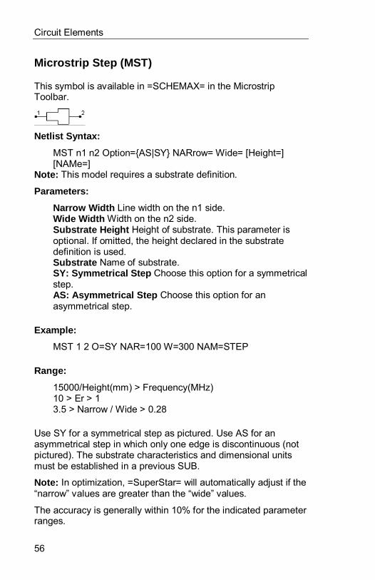
Microstrip Step (MST)
This symbol is available in =SCHEMAX= in the MicrostripToolbar.
Netlist Syntax:
MST n1 n2 Option={AS|SY} NARrow= Wide= [Height=][NAMe=]
Note: This model requires a substrate definition.
Parameters:
Narrow Width Line width on the n1 side.Wide Width Width on the n2 side.Substrate Height Height of substrate. This parameter isoptional. If omitted, the height declared in the substratedefinition is used.Substrate Name of substrate.SY: Symmetrical Step Choose this option for a symmetricalstep.AS: Asymmetrical Step Choose this option for anasymmetrical step.
Example:
MST 1 2 O=SY NAR=100 W=300 NAM=STEP
Range:
15000/Height(mm) > Frequency(MHz)10 > Er > 13.5 > Narrow / Wide > 0.28
Use SY for a symmetrical step as pictured. Use AS for anasymmetrical step in which only one edge is discontinuous (notpictured). The substrate characteristics and dimensional unitsmust be established in a previous SUB.
Note: In optimization, =SuperStar= will automatically adjust if the“narrow” values are greater than the “wide” values.
The accuracy is generally within 10% for the indicated parameterranges.

Microstrip Step (MST)
57
The step is modeled as a series L, Shunt C, series L pi network.
Touchstone Translation:
MSTEP n1 n2 W1= W2= (Symmetrical)None (Asymmetrical)
Default SPICE Translation:
None
Circuit Elements
58
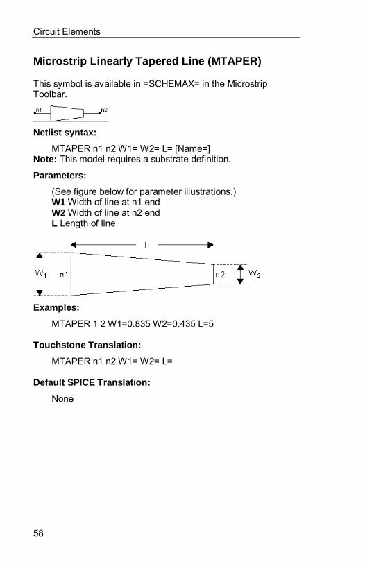
Microstrip Linearly Tapered Line (MTAPER)
This symbol is available in =SCHEMAX= in the MicrostripToolbar.
Netlist syntax:
MTAPER n1 n2 W1= W2= L= [Name=]Note: This model requires a substrate definition.
Parameters:
(See figure below for parameter illustrations.)W1 Width of line at n1 endW2 Width of line at n2 endL Length of line
Examples:
MTAPER 1 2 W1=0.835 W2=0.435 L=5
Touchstone Translation:
MTAPER n1 n2 W1= W2= L=
Default SPICE Translation:
None
Microstrip Tee Junction (MTE)
59
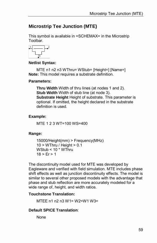
Microstrip Tee Junction (MTE)
This symbol is available in =SCHEMAX= in the MicrostripToolbar.
Netlist Syntax:
MTE n1 n2 n3 WThru= WStub= [Height=] [Name=]Note: This model requires a substrate definition.
Parameters:
Thru Width Width of thru lines (at nodes 1 and 2).Stub Width Width of stub line (at node 3).Substrate Height Height of substrate. This parameter isoptional. If omitted, the height declared in the substratedefinition is used.
Example:
MTE 1 2 3 WT=100 WS=400
Range:
15000/Height(mm) > Frequency(MHz)10 > WThru / Height > 0.1WStub < 10 * WThru18 > Er > 1
The discontinuity model used for MTE was developed byEagleware and verified with field simulation. MTE includes phaseshift effects as well as junction discontinuity effects. The model issimilar to several other proposed models with the advantage thatphase and stub reflection are more accurately modeled for awide range of, height, and width ratios.
Touchstone Translation:
MTEE n1 n2 n3 W1= W2=W1 W3=
Default SPICE Translation :
None

Circuit Elements
60
Two Mutually Coupled Inductors (MUI)
This symbol is available in =SCHEMAX= in the LUMPEDToolbar.
Netlist Syntax:
MUI n1 n2 n3 n4 L1= L2= K= [Name=]
Parameters:
L1 Inductance of coil between n1 and n2 in nanohenries.L2 Inductance of coil between n3 and n4 in nanohenries.Coupling, K Coefficient of coupling.
Warning : “K” must not equal 1.
Example:
MUI 1 2 3 4 L1=100 L2=100 K=.999999
A negative value of “K” inverts the phase. MUI is used to model atransformer including finite winding inductance and coupling,providing for a more realistic model.
Touchstone Translation:
MUC n1 n3 n2 n4 L1= L2= M=
Default SPICE Translation:
.SUBCKT X$NAME 1 2 3 4L_IND1 1 2 L1 nHL_IND2 3 4 L2 nHK_MUI L_IND1 L_IND2 k.ENDS X$NAME
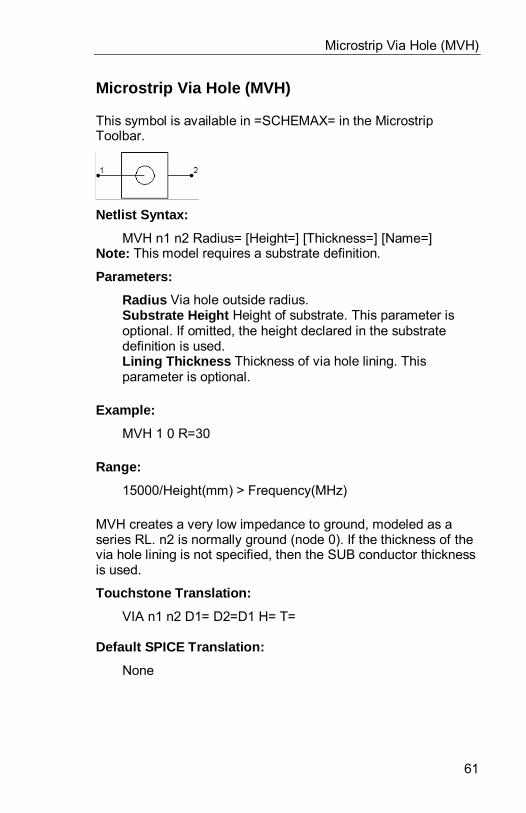
Microstrip Via Hole (MVH)
61
Microstrip Via Hole (MVH)
This symbol is available in =SCHEMAX= in the MicrostripToolbar.
Netlist Syntax:
MVH n1 n2 Radius= [Height=] [Thickness=] [Name=]Note: This model requires a substrate definition.
Parameters:
Radius Via hole outside radius.Substrate Height Height of substrate. This parameter isoptional. If omitted, the height declared in the substratedefinition is used.Lining Thickness Thickness of via hole lining. Thisparameter is optional.
Example:
MVH 1 0 R=30
Range:
15000/Height(mm) > Frequency(MHz)
MVH creates a very low impedance to ground, modeled as aseries RL. n2 is normally ground (node 0). If the thickness of thevia hole lining is not specified, then the SUB conductor thicknessis used.
Touchstone Translation:
VIA n1 n2 D1= D2=D1 H= T=
Default SPICE Translation:
None

Circuit Elements
62
NET Block
This element is only available in =SCHEMAX=. It is accessedfrom the Main =SCHEMAX= Toolbar. It is used to reuse anetwork within a schematic (e.g. for chaining amplifier stages,filters, etc.), and has the symbol shown below:
Parameters:
Network to Reuse Specifies the name of an existingnetwork which should be assigned to this NET block.
N-Port Data File (NPOn)
63
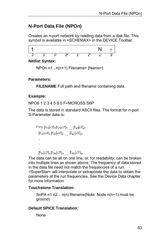
N-Port Data File (NPO n)
Creates an n-port network by reading data from a disk file. Thissymbol is available in =SCHEMAX= in the DEVICE Toolbar.
Netlist Syntax:
NPOn n1...n(n+1) Filename= [Name=]
Parameters:
FILENAME Full path and filename containing data.
Example:
NPO6 1 2 3 4 5 6 0 F=MCROSS.S6P
The data is stored in standard ASCII files. The format for n-portS-Parameter data is:
... ... . . . ...
The data can be all on one line, or, for readability, can be brokeninto multiple lines as shown above. The frequency of data storedin the data file need not match the frequencies of a run.=SuperStar= will interpolate or extrapolate the data to obtain theparameters at the run frequencies. See the Device Data chapterfor more information
Touchstone Translation:
SnPA n1 n2... n(n) filename(Note: Node n(n+1) must beground)
Default SPICE Translation:
None
Circuit Elements
64
1-Port Data File (ONE)
Creates a one port by reading data from a disk file. This symbolis available in =SCHEMAX= in the DEVICE Toolbar.
Netlist Syntax:
ONE n1 n2 Filename= [Name=]
Parameters:
FILENAME Full path and filename containing data.
Example:
ONE 1 0 F=ANTENNA.S1P
The data is stored in standard sequential ASCII files. The formatfor one-port S-Parameter data is:
.
.
.
All magnitudes are linear (not dB), and all angles are indegrees.
The frequency of data stored in the data file need not match thefrequencies of a run. =SuperStar= will interpolate or extrapolatethe data to estimate the parameters at the run frequencies. Seethe Device Data chapter for more information.
Touchstone Translation:
S1PA n1 n2 filename (Note: Node n2 must be ground)
Default SPICE Translation:
None
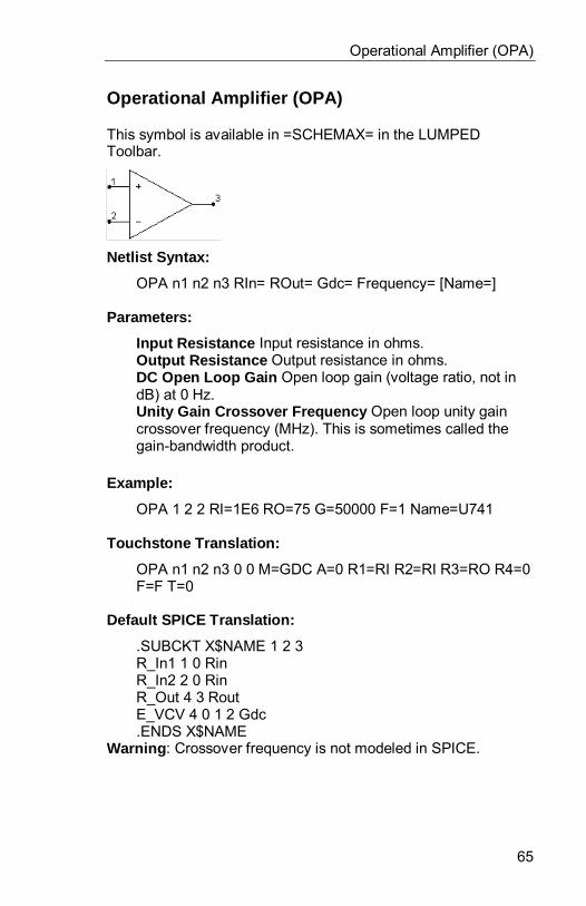
Operational Amplifier (OPA)
65
Operational Amplifier (OPA)
This symbol is available in =SCHEMAX= in the LUMPEDToolbar.
Netlist Syntax:
OPA n1 n2 n3 RIn= ROut= Gdc= Frequency= [Name=]
Parameters:
Input Resistance Input resistance in ohms.Output Resistance Output resistance in ohms.DC Open Loop Gain Open loop gain (voltage ratio, not indB) at 0 Hz.Unity Gain Crossover Frequency Open loop unity gaincrossover frequency (MHz). This is sometimes called thegain-bandwidth product.
Example:
OPA 1 2 2 RI=1E6 RO=75 G=50000 F=1 Name=U741
Touchstone Translation:
OPA n1 n2 n3 0 0 M=GDC A=0 R1=RI R2=RI R3=RO R4=0F=F T=0
Default SPICE Translation:
.SUBCKT X$NAME 1 2 3R_In1 1 0 RinR_In2 2 0 RinR_Out 4 3 RoutE_VCV 4 0 1 2 Gdc.ENDS X$NAME
Warning : Crossover frequency is not modeled in SPICE.
Circuit Elements
66
Parallel L-C resonator (PFC)
There is no symbol for this element in =SCHEMAX=. To createit, you must change the model for another symbol.
Netlist Syntax :
PFC n1 n2 Frequency= C= [Ql=] [Qc=] [Name=]
Parameters:
C Capacitance (pF).Ql Q of the inductor (optional, defaults to 1 million).Qc Q of the capacitor (optional, defaults to 1 million).
Example:
PFC 1 2 F=88 C=100 Ql=35 Qc=600
Q is modeled as constant with frequency and may be specifiedhigher or lower than the default value.
This code generates the same network as PLC. However, thefrequency and capacitance are specified instead of theinductance and capacitance. This is useful for two reasons. First,networks with bandpass and bandstop structures are often ill-behaved for optimization. As the L or C is changed to adjust theL/C ratio, the frequency is perturbed. The use of this resonatorcode can dramatically reduce optimization time in manynetworks, sometimes by as much as an order of magnitude.Secondly, this code is well suited to tuning or optimizing aresponse while leaving a transmission zero or peak at a desiredfrequency.
Parallel L-C resonator (PFL)
67
Parallel L-C resonator (PFL)
There is no symbol for this element in =SCHEMAX=. To createit, you must change the model for another symbol.
Netlist Syntax:
PFL n1 n2 Frequency= L= [Ql=] [Qc=] [Name=]
Parameters:
L Inductance (nH).Ql Q of the inductor (optional, defaults to 1 million).Qc Q of the capacitor (optional, defaults to 1 million).
Example:
PFL 1 2 F=88 L=100 Ql=35 Qc=600
Q is modeled as constant with frequency and may be specifiedhigher or lower than the default value.
This code generates the same network as PLC. However, thefrequency and inductance are specified instead of the inductanceand capacitance. This is useful for two reasons. First, networkswith bandpass and bandstop structures are often ill-behaved foroptimization. As the L or C is changed to adjust the L/C ratio, thefrequency is perturbed. The use of this resonator code candramatically reduce optimization time in many networks,sometimes by as much as an order of magnitude. Secondly, thiscode is well suited to tuning or optimizing a response whileleaving a transmission zero or peak at a desired frequency.

Circuit Elements
68
Ideal Phase Shift (PHASE)
This symbol is available in =SCHEMAX= in the LUMPED toolbar.
Note: n3 is normally grounded.
Netlist syntax:
PHASE n1 n2 n3 A= S= F= [Name=]
Parameters:
A Constant phase shift for 0<FREQ<F (degrees)S Phase slope for FREQ>F (degrees/octave)F Frequency for onset of slope (MHz)
Examples:
PHASE 1 2 0 A=45 S=45 F=5Note: These elements can be cascaded to obtain arbitraryphase responses.
Touchstone Translation:
PHASE n1 n2 A= S= F=
Default SPICE Translation:
None
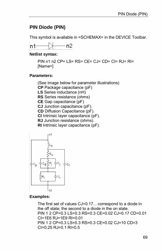
PIN Diode (PIN)
69
PIN Diode (PIN)
This symbol is available in =SCHEMAX= in the DEVICE Toolbar.
Netlist syntax:
PIN n1 n2 CP= LS= RS= CE= CJ= CD= CI= RJ= RI=[Name=]
Parameters:
(See image below for parameter illustrations)CP Package capacitance (pF)LS Series inductance (nH)RS Series resistance (ohms)CE Gap capacitance (pF)CJ Junction capacitance (pF).CD Diffusion Capacitance (pF).CI Intrinsic layer capacitance (pF).RJ Junction resistance (ohms).RI Intrinsic layer capacitance (pF).
Examples:
The first set of values CJ=0.17... correspond to a diode inthe off state; the second to a diode in the on state.PIN 1 2 CP=0.3 LS=0.3 RS=0.3 CE=0.02 CJ=0.17 CD=0.01CI=1E6 RJ=1E9 RI=0.01PIN 1 2 CP=0.3 LS=0.3 RS=0.3 CE=0.02 CJ=10 CD=3CI=0.25 RJ=0.1 RI=0.5

Circuit Elements
70
Touchstone Translation:
PIN n1 n2
Default SPICE Translation:
None
PLC
71
PLC
Parallel inductor and capacitor network. There is no symbol forthis element in =SCHEMAX=. To create it, you must change themodel for another symbol.
Netlist Syntax:
PLC n1 n2 L= C= [Ql=] [Qc=] [Name=]
Parameters:
L Inductance (nH).C Capacitance (pF).Ql Q of the inductor (optional, defaults to 1 million).Qc Q of the capacitor (optional, defaults to 1 million).
Example:
PLC 1 2 L=100 C=22 Ql=35 Qc=600
Q is modeled as constant with frequency and may be specifiedhigher or lower than the default value.
Circuit Elements
72
PRC
Parallel resistor capacitor network. There is no symbol for thiselement in =SCHEMAX=. To create it, you must change themodel for another symbol.
Netlist Syntax:
PRC n1 n2 R= C= [Qc=] [Name=]Parameters:
R Resistance (ohms).C Capacitance (pF).Qc Q of the capacitor (optional, defaults to 1 million).
Example:
PRC 1 2 R=50 C=22 Qc=600
Q is modeled as constant with frequency and may be specifiedhigher or lower than the default value.
PRL
73
PRL
Parallel resistor inductor network. There is no symbol for thiselement in =SCHEMAX=. To create it, you must change themodel for another symbol.
Netlist Syntax:
PRL n1 n2 R= L= [Ql=] [Name=]
Parameters:
R Resistance (ohms).L Inductance (nH).Ql Q of the inductor (optional, defaults to 1 million).
Example:
PRL 1 2 R=50 L=100 Ql=35
Q is modeled as constant with frequency and may be specifiedhigher or lower than the default value.
Circuit Elements
74
PRX
Parallel resistor inductor capacitor network. There is no symbolfor this element in =SCHEMAX=. To create it, you must changethe model for another symbol.
Netlist Syntax:
PRX n1 n2 R= L= C= [Ql=] [Qc=] [Name=]
Parameters:
R Resistance (ohms).L Inductance (nH).C Capacitance (pF).Ql Q of the inductor (optional, defaults to 1 million).Qc Q of the capacitor (optional, defaults to 1 million).
Example:
PRX 1 2 R=50 L=100 C=22 Ql=35 Qc=600
Q is modeled as constant with frequency and may be specifiedhigher or lower than the default value.
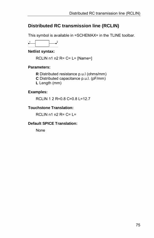
Distributed RC transmission line (RCLIN)
75
Distributed RC transmission line (RCLIN)
This symbol is available in =SCHEMAX= in the TLINE toolbar.
Netlist syntax:
RCLIN n1 n2 R= C= L= [Name=]
Parameters:
R Distributed resistance p.u.l (ohms/mm)C Distributed capacitance p.u.l. (pF/mm)L Length (mm)
Examples:
RCLIN 1 2 R=0.8 C=0.8 L=12.7
Touchstone Translation:
RCLIN n1 n2 R= C= L=
Default SPICE Translation:
None
Circuit Elements
76
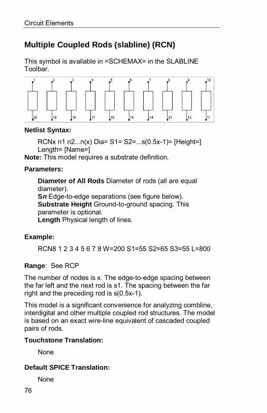
Multiple Coupled Rods (slabline) (RCN)
This symbol is available in =SCHEMAX= in the SLABLINEToolbar.
Netlist Syntax:
RCNx n1 n2...n(x) Dia= S1= S2=...s(0.5x-1)= [Height=]Length= [Name=]
Note: This model requires a substrate definition.
Parameters:
Diameter of All Rods Diameter of rods (all are equaldiameter).Sn Edge-to-edge separations (see figure below).Substrate Height Ground-to-ground spacing. Thisparameter is optional.Length Physical length of lines.
Example:
RCN8 1 2 3 4 5 6 7 8 W=200 S1=55 S2=65 S3=55 L=800
Range : See RCP
The number of nodes is x. The edge-to-edge spacing betweenthe far left and the next rod is s1. The spacing between the farright and the preceding rod is s(0.5x-1).
This model is a significant convenience for analyzing combline,interdigital and other multiple coupled rod structures. The modelis based on an exact wire-line equivalent of cascaded coupledpairs of rods.
Touchstone Translation:
None
Default SPICE Translation:
None
Coupled Slabline (RCP)
77
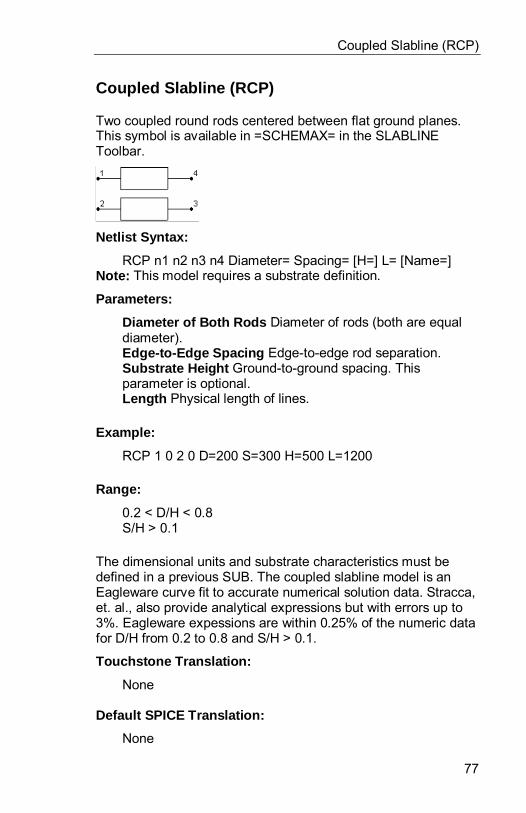
Coupled Slabline (RCP)
Two coupled round rods centered between flat ground planes.This symbol is available in =SCHEMAX= in the SLABLINEToolbar.
Netlist Syntax:
RCP n1 n2 n3 n4 Diameter= Spacing= [H=] L= [Name=]Note: This model requires a substrate definition.
Parameters:
Diameter of Both Rods Diameter of rods (both are equaldiameter).Edge-to-Edge Spacing Edge-to-edge rod separation.Substrate Height Ground-to-ground spacing. Thisparameter is optional.Length Physical length of lines.
Example:
RCP 1 0 2 0 D=200 S=300 H=500 L=1200
Range:
0.2 < D/H < 0.8S/H > 0.1
The dimensional units and substrate characteristics must bedefined in a previous SUB. The coupled slabline model is anEagleware curve fit to accurate numerical solution data. Stracca,et. al., also provide analytical expressions but with errors up to3%. Eagleware expessions are within 0.25% of the numeric datafor D/H from 0.2 to 0.8 and S/H > 0.1.
Touchstone Translation:
None
Default SPICE Translation:
None

Circuit Elements
78
Resistor (RES)
Lumped resistance. This symbol is available in =SCHEMAX= inthe LUMPED Toolbar.
Netlist Syntax:
RES n1 n2 R= [Name=]
Parameters:
Resistance (ohms) Specifies the value of the resistor inohms.
Examples:
RES 1 2 R=22RES 3 0 R=470 N=R1
Touchstone Translation:
RES n1 n2 R=
Default SPICE Translation:
R1_NAME n1 n2 R

Rectangular Wire (RIBBON)
79
Rectangular Wire (RIBBON)
Conducting wire of rectangular cross section. This symbol isavailable in =SCHEMAX= in the TLINE toolbar.
Netlist syntax:
RIBBON n1 n2 W= T= L= RH=[Name=]
Parameters:
W Width of wire (mm).T Thickness of wire (mm).L Length of wire (mm).RH Resistivity of wire relative to copper.
Examples:
RIBBON 1 2 W=0.0394 T=0.00394 L=0.394 RH=1Note: Resistance is d-c resistance or skin effect resistancedepending upon which is larger.
Touchstone Translation:
RIBBON n1 n2 W= L= RHO=RH
Default SPICE Translation:
None

Circuit Elements
80
Slabline (RLI)
Round rod transmission line centered between flat groundplanes. This symbol is available in =SCHEMAX= in theSLABLINE Toolbar.
Netlist Syntax:
RLI n1 n2 Diameter= [Height=] Length= [Name=]Note: This model requires a substrate definition.
Parameters:
Rod Diameter Rod diameter.Substrate Height Ground-to-ground spacing. Thisparameter is optional and defaults to the value specified inthe substrate.Length Physical length of line.
Example:
RLI 1 2 D=200 H=500 L=1200
The dimensional units and substrate characteristics must bedefined in a previous SUB. Slabline is particularly well suited forapplications where a high unloaded Q (low loss) is required. Anapproximate expression due to Frankel has been widely usedsince 1942, but this model is a curve fit to more accuratenumerical solution data. The impedance is believed to be withina fraction of a percent of the precise value for D/H from 0.10 to0.90.
Touchstone Translation:
None
Default SPICE Translation:
None
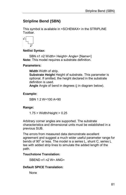
Stripline Bend (SBN)
81
Stripline Bend (SBN)
This symbol is available in =SCHEMAX= in the STRIPLINEToolbar.
Netlist Syntax:
SBN n1 n2 Width= Height= Angle= [Name=]Note: This model requires a substrate definition.
Parameters:
Width Width of strip.Substrate Height Height of substrate. This parameter isoptional. If omitted, the height declared in the substratedefinition is used.Angle Angle of bend in degrees (j in diagram below).
Example:
SBN 1 2 W=100 A=90
Range:
1.75 > Width/Height > 0.25
Arbitrary corner angles are supported. The substratecharacteristics and dimensional units must be established in aprevious SUB.
The errors from measured data demonstrate excellentagreement and suggest a much wider useful parameter range forbends of 90o or less. The model is a series L, shunt C, series Ltee with added strip lines to simulate the added length of thepath.
Touchstone Translation:
SBEND n1 n2 W= ANG=
Default SPICE Translation:
None
Circuit Elements
82
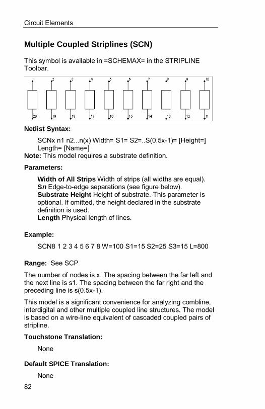
Multiple Coupled Striplines (SCN)
This symbol is available in =SCHEMAX= in the STRIPLINEToolbar.
Netlist Syntax:
SCNx n1 n2...n(x) Width= S1= S2=..S(0.5x-1)= [Height=]Length= [Name=]
Note: This model requires a substrate definition.
Parameters:
Width of All Strips Width of strips (all widths are equal).Sn Edge-to-edge separations (see figure below).Substrate Height Height of substrate. This parameter isoptional. If omitted, the height declared in the substratedefinition is used.Length Physical length of lines.
Example:
SCN8 1 2 3 4 5 6 7 8 W=100 S1=15 S2=25 S3=15 L=800
Range: See SCP
The number of nodes is x. The spacing between the far left andthe next line is s1. The spacing between the far right and thepreceding line is s(0.5x-1).
This model is a significant convenience for analyzing combline,interdigital and other multiple coupled line structures. The modelis based on a wire-line equivalent of cascaded coupled pairs ofstripline.
Touchstone Translation:
None
Default SPICE Translation:
None
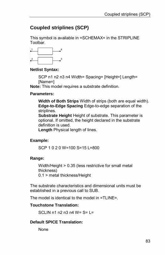
Coupled striplines (SCP)
83
Coupled striplines (SCP)
This symbol is available in =SCHEMAX= in the STRIPLINEToolbar.
Netlist Syntax:
SCP n1 n2 n3 n4 Width= Spacing= [Height=] Length=[Name=]
Note: This model requires a substrate definition.
Parameters:
Width of Both Strips Width of strips (both are equal width).Edge-to-Edge Spacing Edge-to-edge separation of thestriplines.Substrate Height Height of substrate. This parameter isoptional. If omitted, the height declared in the substratedefinition is used.Length Physical length of lines.
Example:
SCP 1 0 2 0 W=100 S=15 L=800
Range:
Width/Height > 0.35 (less restrictive for small metalthickness)0.1 > metal thickness/Height
The substrate characteristics and dimensional units must beestablished in a previous call to SUB.
The model is identical to the model in =TLINE=.
Touchstone Translation:
SCLIN n1 n2 n3 n4 W= S= L=
Default SPICE Translation:
None
Circuit Elements
84
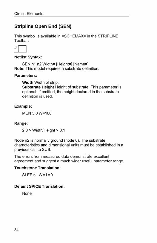
Stripline Open End (SEN)
This symbol is available in =SCHEMAX= in the STRIPLINEToolbar.
Netlist Syntax:
SEN n1 n2 Width= [Height=] [Name=]Note: This model requires a substrate definition.
Parameters:
Width Width of strip.Substrate Height Height of substrate. This parameter isoptional. If omitted, the height declared in the substratedefinition is used.
Example:
MEN 5 0 W=100
Range:
2.0 > Width/Height > 0.1
Node n2 is normally ground (node 0). The substratecharacteristics and dimensional units must be established in aprevious call to SUB.
The errors from measured data demonstrate excellentagreement and suggest a much wider useful parameter range.
Touchstone Translation:
SLEF n1 W= L=0
Default SPICE Translation:
None
SFC
85
SFC
Series L-C resonator. There is no symbol for this element in=SCHEMAX=. To create it, you must change the model foranother symbol.
Netlist Syntax:
SFC n1 n2 Frequency= C= [Ql=] [Qc=] [Name=]
Parameters:
C Capacitance (pF).Ql Q of the inductor (optional, defaults to 1 million).Qc Q of the capacitor (optional, defaults to 1 million).
Example:
SFC 1 2 F=88 C=22 Ql=35 Qc=600
Q is modeled as constant with frequency and may be specifiedhigher or lower than the default value.
This code generates the same network as SLC. However, thefrequency and capacitance are specified instead of theinductance and capacitance. This is useful for two reasons. First,networks with bandpass and bandstop structures are often ill-behaved for optimization. As the L or C is changed to adjust theL/C ratio, the frequency is perturbed. The use of this resonatorcode can dramatically reduce optimization time in manynetworks, sometimes by as much as an order of magnitude.Secondly, this code is well suited to tuning or optimizing aresponse while leaving a transmission zero or peak at a desiredfrequency.
Circuit Elements
86
SFL
Series L-C resonator. There is no symbol for this element in=SCHEMAX=. To create it, you must change the model foranother symbol.
Netlist Syntax:
SFL n1 n2 Frequency= L= [Ql=] [Qc=] [Name=]
Parameters:
L Inductance (nH).Ql Q of the inductor (optional, defaults to 1 million).Qc Q of the capacitor (optional, defaults to 1 million).
Example:
SFL 1 2 F=88 L=100 Ql=35 Qc=600
Q is modeled as constant with frequency and may be specifiedhigher or lower than the default value.
This code generates the same network as SLC. However, thefrequency and inductance are specified instead of the inductanceand capacitance. This is useful for two reasons. First, networkswith bandpass and bandstop structures are often ill-behaved foroptimization. As the L or C is changed to adjust the L/C ratio, thefrequency is perturbed. The use of this resonator code candramatically reduce optimization time in many networks,sometimes by as much as an order of magnitude. Secondly, thiscode is well suited to tuning or optimizing a response whileleaving a transmission zero or peak at a desired frequency.
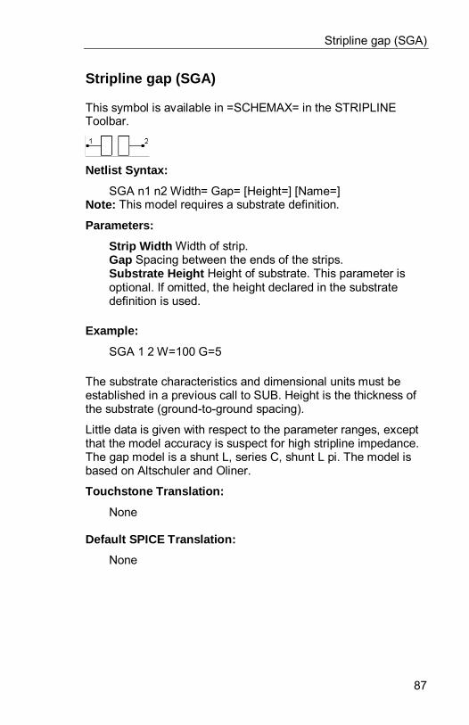
Stripline gap (SGA)
87
Stripline gap (SGA)
This symbol is available in =SCHEMAX= in the STRIPLINEToolbar.
Netlist Syntax:
SGA n1 n2 Width= Gap= [Height=] [Name=]Note: This model requires a substrate definition.
Parameters:
Strip Width Width of strip.Gap Spacing between the ends of the strips.Substrate Height Height of substrate. This parameter isoptional. If omitted, the height declared in the substratedefinition is used.
Example:
SGA 1 2 W=100 G=5
The substrate characteristics and dimensional units must beestablished in a previous call to SUB. Height is the thickness ofthe substrate (ground-to-ground spacing).
Little data is given with respect to the parameter ranges, exceptthat the model accuracy is suspect for high stripline impedance.The gap model is a shunt L, series C, shunt L pi. The model isbased on Altschuler and Oliner.
Touchstone Translation:
None
Default SPICE Translation:
None
Circuit Elements
88
Series inductor and capacitor network (SLC)
There is no symbol for this element in =SCHEMAX=. To createit, you must change the model for another symbol.
Netlist Syntax:
SLC n1 n2 L= C= [Ql=] [Qc=] [Name=]
Parameters:
L Inductance (nH).C Capacitance (pF).Ql Q of the inductor (optional, defaults to 1 million).Qc Q of the capacitor (optional, defaults to 1 million).
Example:
SRL 1 2 L=100 C=22 Ql=35 Qc=600
Q is modeled as constant with frequency and may be specifiedhigher or lower than the default value.
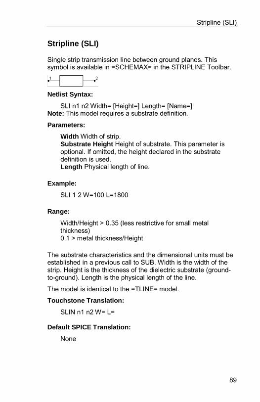
Stripline (SLI)
89
Stripline (SLI)
Single strip transmission line between ground planes. Thissymbol is available in =SCHEMAX= in the STRIPLINE Toolbar.
Netlist Syntax:
SLI n1 n2 Width= [Height=] Length= [Name=]Note: This model requires a substrate definition.
Parameters:
Width Width of strip.Substrate Height Height of substrate. This parameter isoptional. If omitted, the height declared in the substratedefinition is used.Length Physical length of line.
Example:
SLI 1 2 W=100 L=1800
Range:
Width/Height > 0.35 (less restrictive for small metalthickness)0.1 > metal thickness/Height
The substrate characteristics and the dimensional units must beestablished in a previous call to SUB. Width is the width of thestrip. Height is the thickness of the dielectric substrate (ground-to-ground). Length is the physical length of the line.
The model is identical to the =TLINE= model.
Touchstone Translation:
SLIN n1 n2 W= L=
Default SPICE Translation:
None
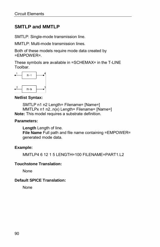
Circuit Elements
90
SMTLP and MMTLP
SMTLP: Single-mode transmission line.
MMTLP: Multi-mode transmission lines.
Both of these models require mode data created by=EMPOWER=.
These symbols are available in =SCHEMAX= in the T-LINEToolbar.
Netlist Syntax:
SMTLP n1 n2 Length= Filename= [Name=]MMTLPx n1 n2..n(x) Length= Filename= [Name=]
Note: This model requires a substrate definition.
Parameters:
Length Length of line.File Name Full path and file name containing =EMPOWER=generated mode data.
Example:
MMTLP4 6 12 1 5 LENGTH=100 FILENAME=PART1.L2
Touchstone Translation:
None
Default SPICE Translation:
None
S-parameters (SPA)
91
S-parameters (SPA)
There is no symbol for this element in =SCHEMAX=. To createit, you must change the model for another symbol.
Netlist Syntax :
SPA 1 2 0 Z= MAG11= ANG11= MAG21= ANG21=MAG12= ANG12= MAG22= ANG22=
Parameters:
Z Reference Impedance (Ohms).MAG11 S11 magnitude.ANG11 S11 phase (degrees).MAG21 S21 magnitude.ANG21 S21 phase (degrees).MAG12 S12 magnitude.ANG12 S12 phase (degrees).MAG22 S22 magnitude.ANG22 S22 phase (degrees).
Example:
SPA 1 2 0 Z=50 MAG11=.2 ANG11=15 MAG21=2ANG21=90 MAG12=.15 ANG12=-45 MAG22=2 ANG22=90
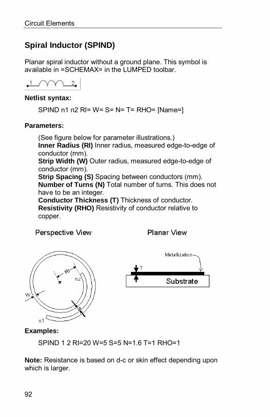
Circuit Elements
92
Spiral Inductor (SPIND)
Planar spiral inductor without a ground plane. This symbol isavailable in =SCHEMAX= in the LUMPED toolbar.
Netlist syntax:
SPIND n1 n2 RI= W= S= N= T= RHO= [Name=]
Parameters:
(See figure below for parameter illustrations.)Inner Radius (RI) Inner radius, measured edge-to-edge ofconductor (mm).Strip Width (W) Outer radius, measured edge-to-edge ofconductor (mm).Strip Spacing (S) Spacing between conductors (mm).Number of Turns (N) Total number of turns. This does nothave to be an integer.Conductor Thickn ess (T) Thickness of conductor.Resistivity (RHO) Resistivity of conductor relative tocopper.
Examples:
SPIND 1 2 RI=20 W=5 S=5 N=1.6 T=1 RHO=1
Note: Resistance is based on d-c or skin effect depending uponwhich is larger.

Spiral Inductor (SPIND)
93
Series R-L with inductance (self and mutual) determined byRemke and Burdick formulas. Resistance is d-c resistance orskin-effect resistance, whichever is greater.
Touchstone Translation:
None
Default SPICE Translation:
None
Circuit Elements
94
SRC
Series resistor and capacitor network. There is no symbol for thiselement in =SCHEMAX=. To create it, you must change themodel for another symbol.
Netlist Syntax:
SRC n1 n2 R= C= [Qc=] [Name=]
Parameters:
R Resistance (ohms).C Capacitance (pF).Qc Q of the capacitor (optional, defaults to 1 million).
Example:
SRC 1 2 R=50 L=22 Qc=600
Q is modeled as constant with frequency and may be specifiedhigher or lower than the default value.
SRL
95
SRL
Series resistor and inductor network. There is no symbol for thiselement in =SCHEMAX=. To create it, you must change themodel for another symbol.
Netlist Syntax:
SRL n1 n2 R= L= [Ql=] [Name=]
Parameters:
R Resistance (ohms).L Inductance (nH).Ql Q of the inductor (optional, defaults to 1 million).
Example:
SRL 1 2 R=50 L=100 Ql=35
Q is modeled as constant with frequency and may be specifiedhigher or lower than the default value.
Circuit Elements
96
SRX
Series resistor, inductor and capacitor network. There is nosymbol for this element in =SCHEMAX=. To create it, you mustchange the model for another symbol.
Netlist Syntax:
SRX n1 n2 R= L= C= [Ql=] [Qc=] [Name=]
Parameters:
R Resistance (ohms).L Inductance (nH).C Capacitance (pF).Ql Q of the inductor (optional, defaults to 1 million).Qc Q of the capacitor (optional, defaults to 1 million).
Example:
SRX 1 2 R=50 L=100 C=50 Ql=35
Q is modeled as constant with frequency and may be specifiedhigher or lower than the default value.
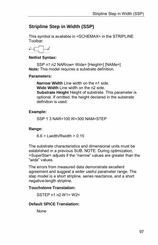
Stripline Step in Width (SSP)
97
Stripline Step in Width (SSP)
This symbol is available in =SCHEMAX= in the STRIPLINEToolbar.
Netlist Syntax:
SSP n1 n2 NARrow= Wide= [Height=] [NAMe=]Note: This model requires a substrate definition.
Parameters:
Narrow Width Line width on the n1 side.Wide Width Line width on the n2 side.Substrate Height Height of substrate. This parameter isoptional. If omitted, the height declared in the substratedefinition is used.
Example:
SSP 1 3 NAR=100 W=300 NAM=STEP
Range:
6.6 > Lwidth/Rwidth > 0.15
The substrate characteristics and dimensional units must beestablished in a previous SUB. NOTE: During optimization,=SuperStar= adjusts if the “narrow” values are greater than the“wide” values.
The errors from measured data demonstrate excellentagreement and suggest a wider useful parameter range. Thestep model is a short stripline, series reactance, and a shortnegative-length stripline.
Touchstone Translation:
SSTEP n1 n2 W1= W2=
Default SPICE Translation:
None
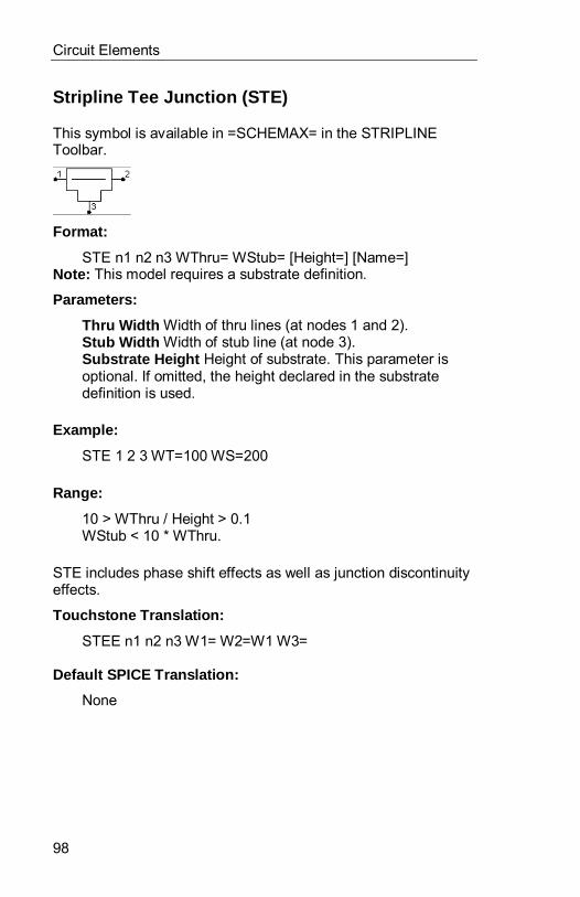
Circuit Elements
98
Stripline Tee Junction (STE)
This symbol is available in =SCHEMAX= in the STRIPLINEToolbar.
Format:
STE n1 n2 n3 WThru= WStub= [Height=] [Name=]Note: This model requires a substrate definition.
Parameters:
Thru Width Width of thru lines (at nodes 1 and 2).Stub Width Width of stub line (at node 3).Substrate Height Height of substrate. This parameter isoptional. If omitted, the height declared in the substratedefinition is used.
Example:
STE 1 2 3 WT=100 WS=200
Range:
10 > WThru / Height > 0.1WStub < 10 * WThru.
STE includes phase shift effects as well as junction discontinuityeffects.
Touchstone Translation:
STEE n1 n2 n3 W1= W2=W1 W3=
Default SPICE Translation:
None
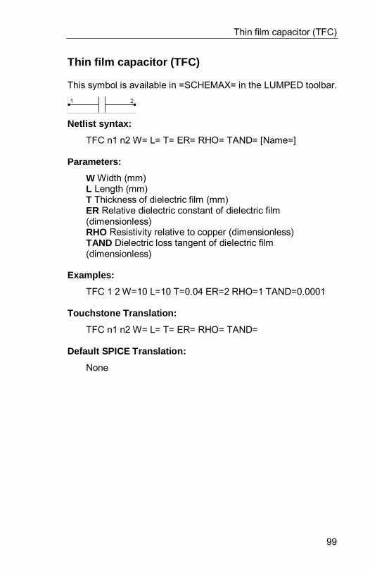
Thin film capacitor (TFC)
99
Thin film capacitor (TFC)
This symbol is available in =SCHEMAX= in the LUMPED toolbar.
Netlist syntax:
TFC n1 n2 W= L= T= ER= RHO= TAND= [Name=]
Parameters:
W Width (mm)L Length (mm)T Thickness of dielectric film (mm)ER Relative dielectric constant of dielectric film(dimensionless)RHO Resistivity relative to copper (dimensionless)TAND Dielectric loss tangent of dielectric film(dimensionless)
Examples:
TFC 1 2 W=10 L=10 T=0.04 ER=2 RHO=1 TAND=0.0001
Touchstone Translation:
TFC n1 n2 W= L= T= ER= RHO= TAND=
Default SPICE Translation:
None
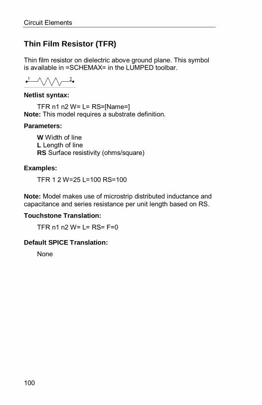
Circuit Elements
100
Thin Film Resistor (TFR)
Thin film resistor on dielectric above ground plane. This symbolis available in =SCHEMAX= in the LUMPED toolbar.
Netlist syntax:
TFR n1 n2 W= L= RS=[Name=]Note: This model requires a substrate definition.
Parameters:
W Width of lineL Length of lineRS Surface resistivity (ohms/square)
Examples:
TFR 1 2 W=25 L=100 RS=100
Note: Model makes use of microstrip distributed inductance andcapacitance and series resistance per unit length based on RS.
Touchstone Translation:
TFR n1 n2 W= L= RS= F=0
Default SPICE Translation:
None
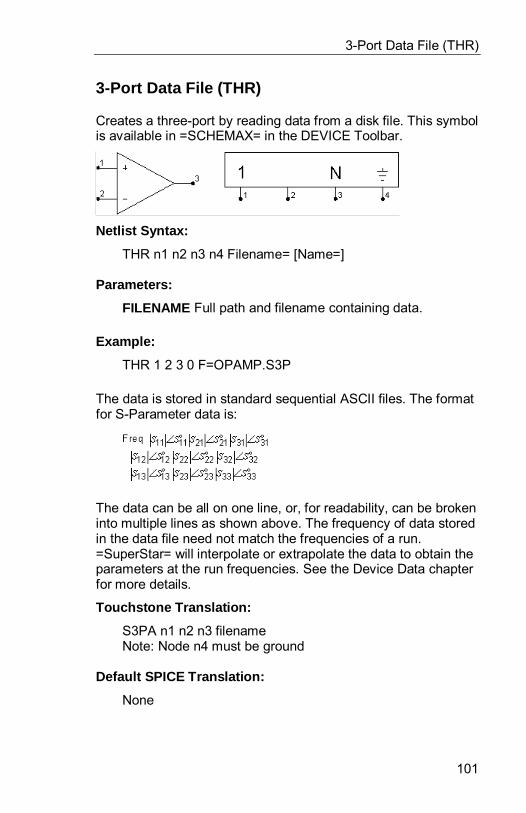
3-Port Data File (THR)
101
3-Port Data File (THR)
Creates a three-port by reading data from a disk file. This symbolis available in =SCHEMAX= in the DEVICE Toolbar.
Netlist Syntax:
THR n1 n2 n3 n4 Filename= [Name=]
Parameters:
FILENAME Full path and filename containing data.
Example:
THR 1 2 3 0 F=OPAMP.S3P
The data is stored in standard sequential ASCII files. The formatfor S-Parameter data is:
The data can be all on one line, or, for readability, can be brokeninto multiple lines as shown above. The frequency of data storedin the data file need not match the frequencies of a run.=SuperStar= will interpolate or extrapolate the data to obtain theparameters at the run frequencies. See the Device Data chapterfor more details.
Touchstone Translation:
S3PA n1 n2 n3 filenameNote: Node n4 must be ground
Default SPICE Translation:
None
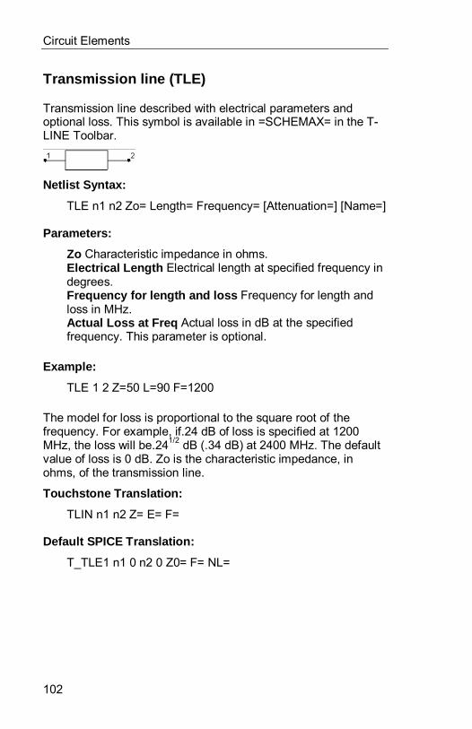
Circuit Elements
102
Transmission line (TLE)
Transmission line described with electrical parameters andoptional loss. This symbol is available in =SCHEMAX= in the T-LINE Toolbar.
Netlist Syntax:
TLE n1 n2 Zo= Length= Frequency= [Attenuation=] [Name=]
Parameters:
Zo Characteristic impedance in ohms.Electrical Length Electrical length at specified frequency indegrees.Frequency for length and loss Frequency for length andloss in MHz.Actual Loss at Freq Actual loss in dB at the specifiedfrequency. This parameter is optional.
Example:
TLE 1 2 Z=50 L=90 F=1200
The model for loss is proportional to the square root of thefrequency. For example, if.24 dB of loss is specified at 1200MHz, the loss will be.241/2 dB (.34 dB) at 2400 MHz. The defaultvalue of loss is 0 dB. Zo is the characteristic impedance, inohms, of the transmission line.
Touchstone Translation:
TLIN n1 n2 Z= E= F=
Default SPICE Translation:
T_TLE1 n1 0 n2 0 Z0= F= NL=
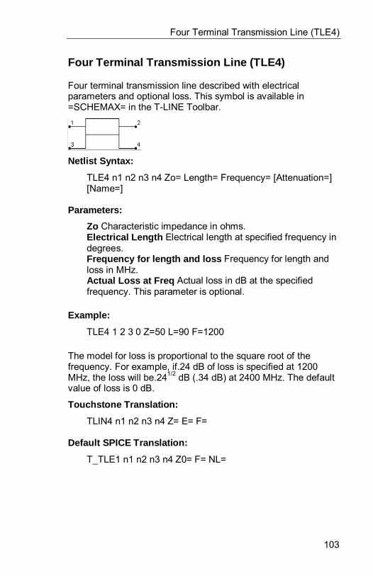
Four Terminal Transmission Line (TLE4)
103
Four Terminal Transmission Line (TLE4)
Four terminal transmission line described with electricalparameters and optional loss. This symbol is available in=SCHEMAX= in the T-LINE Toolbar.
Netlist Syntax:
TLE4 n1 n2 n3 n4 Zo= Length= Frequency= [Attenuation=][Name=]
Parameters:
Zo Characteristic impedance in ohms.Electrical Length Electrical length at specified frequency indegrees.Frequency for length and loss Frequency for length andloss in MHz.Actual Loss at Freq Actual loss in dB at the specifiedfrequency. This parameter is optional.
Example:
TLE4 1 2 3 0 Z=50 L=90 F=1200
The model for loss is proportional to the square root of thefrequency. For example, if.24 dB of loss is specified at 1200MHz, the loss will be.241/2 dB (.34 dB) at 2400 MHz. The defaultvalue of loss is 0 dB.
Touchstone Translation:
TLIN4 n1 n2 n3 n4 Z= E= F=
Default SPICE Translation:
T_TLE1 n1 n2 n3 n4 Z0= F= NL=
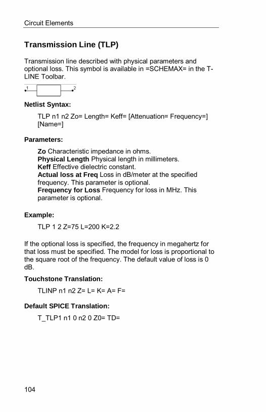
Circuit Elements
104
Transmission Line (TLP)
Transmission line described with physical parameters andoptional loss. This symbol is available in =SCHEMAX= in the T-LINE Toolbar.
Netlist Syntax:
TLP n1 n2 Zo= Length= Keff= [Attenuation= Frequency=][Name=]
Parameters:
Zo Characteristic impedance in ohms.Physical Length Physical length in millimeters.Keff Effective dielectric constant.Actual loss at Freq Loss in dB/meter at the specifiedfrequency. This parameter is optional.Frequency for Loss Frequency for loss in MHz. Thisparameter is optional.
Example:
TLP 1 2 Z=75 L=200 K=2.2
If the optional loss is specified, the frequency in megahertz forthat loss must be specified. The model for loss is proportional tothe square root of the frequency. The default value of loss is 0dB.
Touchstone Translation:
TLINP n1 n2 Z= L= K= A= F=
Default SPICE Translation:
T_TLP1 n1 0 n2 0 Z0= TD=
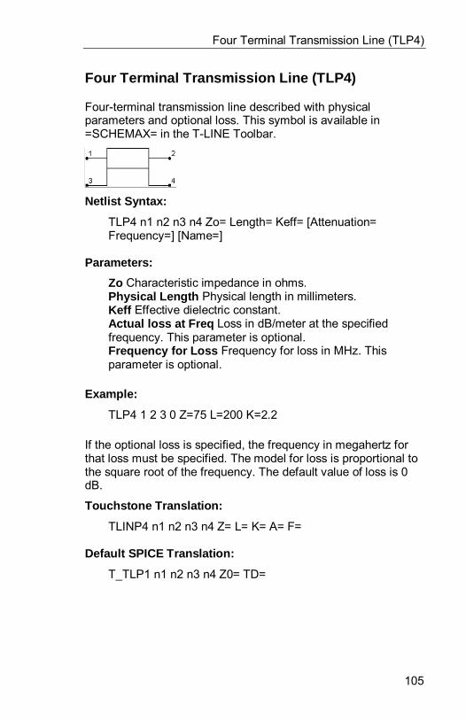
Four Terminal Transmission Line (TLP4)
105
Four Terminal Transmission Line (TLP4)
Four-terminal transmission line described with physicalparameters and optional loss. This symbol is available in=SCHEMAX= in the T-LINE Toolbar.
Netlist Syntax:
TLP4 n1 n2 n3 n4 Zo= Length= Keff= [Attenuation=Frequency=] [Name=]
Parameters:
Zo Characteristic impedance in ohms.Physical Length Physical length in millimeters.Keff Effective dielectric constant.Actual loss at Freq Loss in dB/meter at the specifiedfrequency. This parameter is optional.Frequency for Loss Frequency for loss in MHz. Thisparameter is optional.
Example:
TLP4 1 2 3 0 Z=75 L=200 K=2.2
If the optional loss is specified, the frequency in megahertz forthat loss must be specified. The model for loss is proportional tothe square root of the frequency. The default value of loss is 0dB.
Touchstone Translation:
TLINP4 n1 n2 n3 n4 Z= L= K= A= F=
Default SPICE Translation:
T_TLP1 n1 n2 n3 n4 Z0= TD=
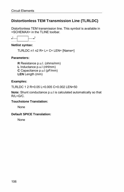
Circuit Elements
106
Distortionless TEM Transmission Line (TLRLDC)
Distortionless TEM transmission line. This symbol is available in=SCHEMAX= in the TLINE toolbar.
Netlist syntax:
TLRLDC n1 n2 R= L= C= LEN= [Name=]
Parameters:
R Resistance p.u.l. (ohms/mm)L Inductance p.u.l (nH/mm)C Capacitance p.u.l (pF/mm)LEN Length (mm)
Examples:
TLRLDC 1 2 R=0.05 L=0.005 C=0.002 LEN=50
Note: Shunt conductance p.u.l is calculated automatically so thatR/L=G/C.
Touchstone Translation:
None
Default SPICE Translation:
None
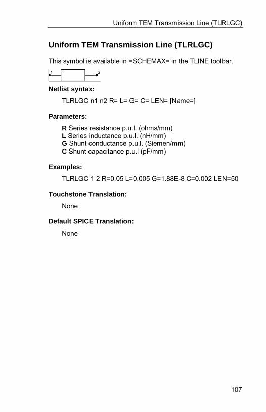
Uniform TEM Transmission Line (TLRLGC)
107
Uniform TEM Transmission Line (TLRLGC)
This symbol is available in =SCHEMAX= in the TLINE toolbar.
Netlist syntax:
TLRLGC n1 n2 R= L= G= C= LEN= [Name=]
Parameters:
R Series resistance p.u.l. (ohms/mm)L Series inductance p.u.l. (nH/mm)G Shunt conductance p.u.l. (Siemen/mm)C Shunt capacitance p.u.l (pF/mm)
Examples:
TLRLGC 1 2 R=0.05 L=0.005 G=1.88E-8 C=0.002 LEN=50
Touchstone Translation:
None
Default SPICE Translation:
None
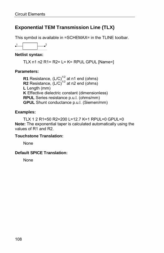
Circuit Elements
108
Exponential TEM Transmission Line (TLX)
This symbol is available in =SCHEMAX= in the TLINE toolbar.
Netlist syntax:
TLX n1 n2 R1= R2= L= K= RPUL GPUL [Name=]
Parameters:
R1 Resistance, (L/C)1/2 at n1 end (ohms)R2 Resistance, (L/C)1/2 at n2 end (ohms)L Length (mm)K Effective dielectric constant (dimensionless)RPUL Series resistance p.u.l. (ohms/mm)GPUL Shunt conductance p.u.l. (Siemen/mm)
Examples:
TLX 1 2 R1=50 R2=200 L=12.7 K=1 RPUL=0 GPUL=0Note: The exponential taper is calculated automatically using thevalues of R1 and R2.
Touchstone Translation:
None
Default SPICE Translation:
None
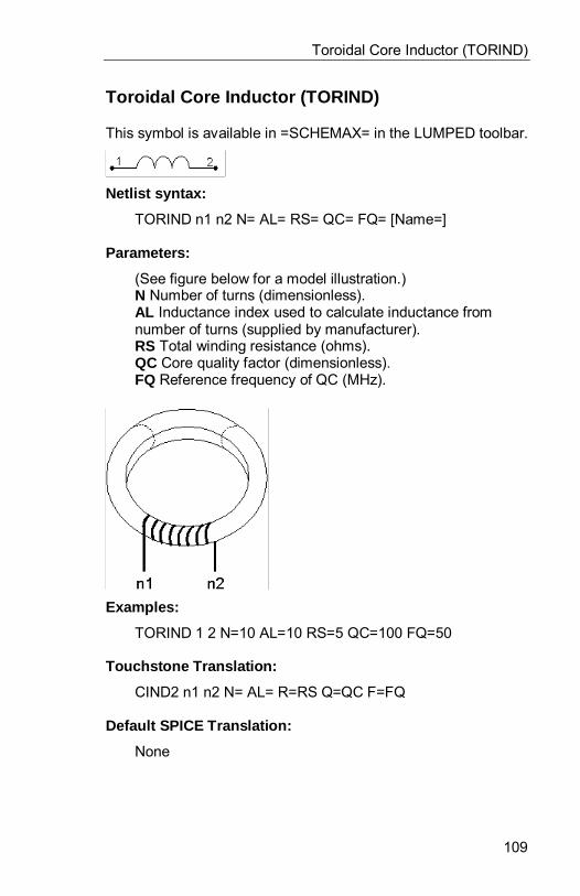
Toroidal Core Inductor (TORIND)
109
Toroidal Core Inductor (TORIND)
This symbol is available in =SCHEMAX= in the LUMPED toolbar.
Netlist syntax:
TORIND n1 n2 N= AL= RS= QC= FQ= [Name=]
Parameters:
(See figure below for a model illustration.)N Number of turns (dimensionless).AL Inductance index used to calculate inductance fromnumber of turns (supplied by manufacturer).RS Total winding resistance (ohms).QC Core quality factor (dimensionless).FQ Reference frequency of QC (MHz).
Examples:
TORIND 1 2 N=10 AL=10 RS=5 QC=100 FQ=50
Touchstone Translation:
CIND2 n1 n2 N= AL= R=RS Q=QC F=FQ
Default SPICE Translation:
None
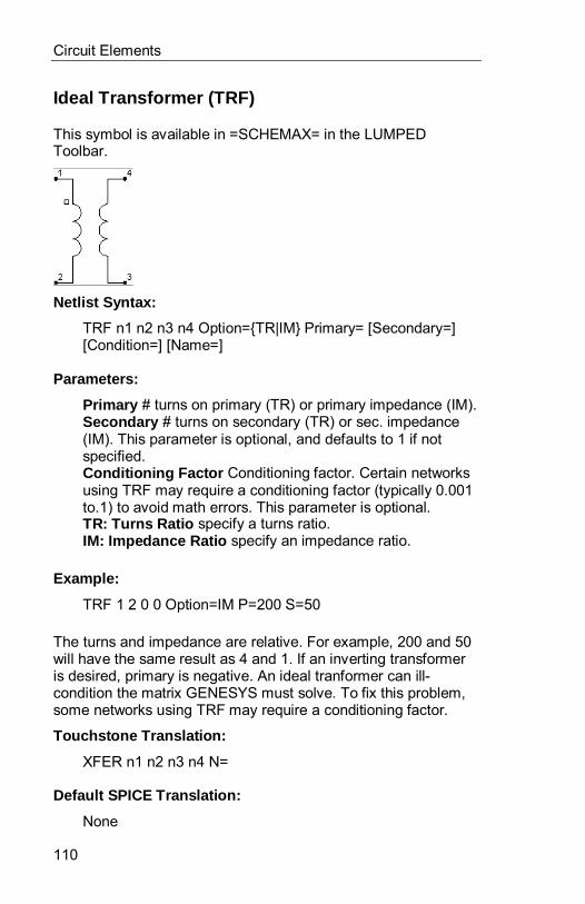
Circuit Elements
110
Ideal Transformer (TRF)
This symbol is available in =SCHEMAX= in the LUMPEDToolbar.
Netlist Syntax:
TRF n1 n2 n3 n4 Option={TR|IM} Primary= [Secondary=][Condition=] [Name=]
Parameters:
Primary # turns on primary (TR) or primary impedance (IM).Secondary # turns on secondary (TR) or sec. impedance(IM). This parameter is optional, and defaults to 1 if notspecified.Conditioning Factor Conditioning factor. Certain networksusing TRF may require a conditioning factor (typically 0.001to.1) to avoid math errors. This parameter is optional.TR: Turns Ratio specify a turns ratio.IM: Impedance Ratio specify an impedance ratio.
Example:
TRF 1 2 0 0 Option=IM P=200 S=50
The turns and impedance are relative. For example, 200 and 50will have the same result as 4 and 1. If an inverting transformeris desired, primary is negative. An ideal tranformer can ill-condition the matrix GENESYS must solve. To fix this problem,some networks using TRF may require a conditioning factor.
Touchstone Translation:
XFER n1 n2 n3 n4 N=
Default SPICE Translation:
None
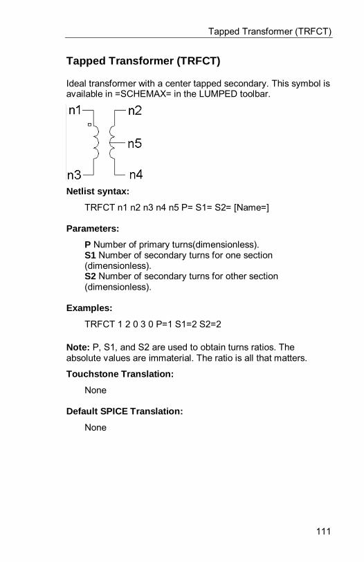
Tapped Transformer (TRFCT)
111
Tapped Transformer (TRFCT)
Ideal transformer with a center tapped secondary. This symbol isavailable in =SCHEMAX= in the LUMPED toolbar.
Netlist syntax:
TRFCT n1 n2 n3 n4 n5 P= S1= S2= [Name=]
Parameters:
P Number of primary turns(dimensionless).S1 Number of secondary turns for one section(dimensionless).S2 Number of secondary turns for other section(dimensionless).
Examples:
TRFCT 1 2 0 3 0 P=1 S1=2 S2=2
Note: P, S1, and S2 are used to obtain turns ratios. Theabsolute values are immaterial. The ratio is all that matters.
Touchstone Translation:
None
Default SPICE Translation:
None

Circuit Elements
112
Ruthroff transformer (TRFRUTH)
Ruthroff transformer modeled as a transmission line (TLE4) withshunt inductance. This symbol is available in =SCHEMAX= inthe T-LINE toolbar.
Netlist Syntax :
TRFRUTH n1 n2 n3 N= AL= Z= L= F=[Name=]
Parameters:
Number of Turns Total number of turns (dimensionless).Inductance Index Inductance index (nH/turn/turn). Thisnumber is used to calculate the equivalent shunt inductance.Transmission Line Zo (Ohms) Characteristic impedance ofthe transmission line in ohms.Electrical Line Length Electrical length of the transmissionline at the specified frequency, in degrees.Frequency for Electrical Length Frequency for the givenelectrical length, in MHz.
Example:
TRFRUTH 1 2 3 N=1 AL=1 Z=2 L=45 F=1000
This is an ideal model based on the paper by Ruthroff. The shuntinductance is given by:
L = N2*AL.
Touchstone Translation:
XFERRUTH N=N AL=AL Z=Z E=L F=F
SPICE Translation:
None
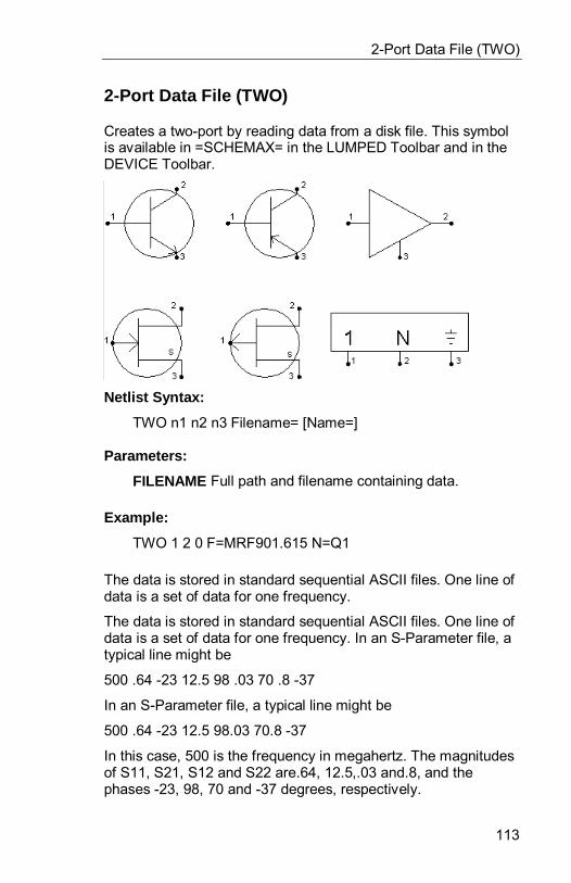
2-Port Data File (TWO)
113
2-Port Data File (TWO)
Creates a two-port by reading data from a disk file. This symbolis available in =SCHEMAX= in the LUMPED Toolbar and in theDEVICE Toolbar.
Netlist Syntax:
TWO n1 n2 n3 Filename= [Name=]
Parameters:
FILENAME Full path and filename containing data.
Example:
TWO 1 2 0 F=MRF901.615 N=Q1
The data is stored in standard sequential ASCII files. One line ofdata is a set of data for one frequency.
The data is stored in standard sequential ASCII files. One line ofdata is a set of data for one frequency. In an S-Parameter file, atypical line might be
500 .64 -23 12.5 98 .03 70 .8 -37
In an S-Parameter file, a typical line might be
500 .64 -23 12.5 98.03 70.8 -37
In this case, 500 is the frequency in megahertz. The magnitudesof S11, S21, S12 and S22 are.64, 12.5,.03 and.8, and thephases -23, 98, 70 and -37 degrees, respectively.

Circuit Elements
114
The frequency of data stored in the data file need not match thefrequencies of a run. =SuperStar= will interpolate or extrapolatethe data to obtain the parameters at the run frequencies. See theDevice Data chapter for more details.
Touchstone Translation:
S2PA n1 n2 n3 filename
Default SPICE Translation:
None
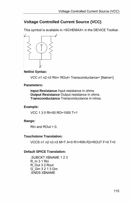
Voltage Controlled Current Source (VCC)
115
Voltage Controlled Current Source (VCC)
This symbol is available in =SCHEMAX= in the DEVICE Toolbar.
Netlist Syntax:
VCC n1 n2 n3 RIn= ROut= Transconductance= [Name=]
Parameters:
Input Resistance Input resistance in ohms.Output Resistance Output resistance in ohms.Transconductance Transconductance in mhos.
Example:
VCC 1 3 0 RI=50 RO=1000 T=1
Range:
RIn and ROut > 0.
Touchstone Translation:
VCCS n1 n2 n3 n3 M=T A=0 R1=RIN R2=ROUT F=0 T=0
Default SPICE Translation:
.SUBCKT X$NAME 1 2 3R_In 3 1 RinR_Out 3 2 RoutG_Gm 3 2 1 3 Gm.ENDS X$NAME
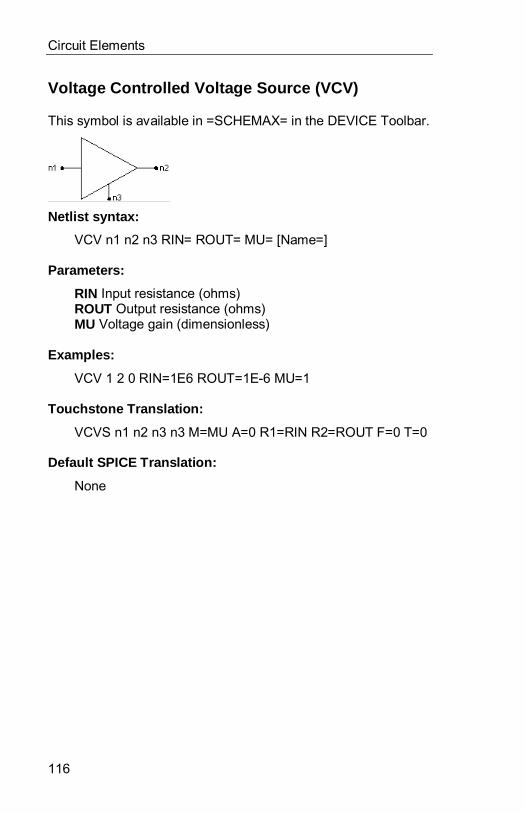
Circuit Elements
116
Voltage Controlled Voltage Source (VCV)
This symbol is available in =SCHEMAX= in the DEVICE Toolbar.
Netlist syntax:
VCV n1 n2 n3 RIN= ROUT= MU= [Name=]
Parameters:
RIN Input resistance (ohms)ROUT Output resistance (ohms)MU Voltage gain (dimensionless)
Examples:
VCV 1 2 0 RIN=1E6 ROUT=1E-6 MU=1
Touchstone Translation:
VCVS n1 n2 n3 n3 M=MU A=0 R1=RIN R2=ROUT F=0 T=0
Default SPICE Translation:
None
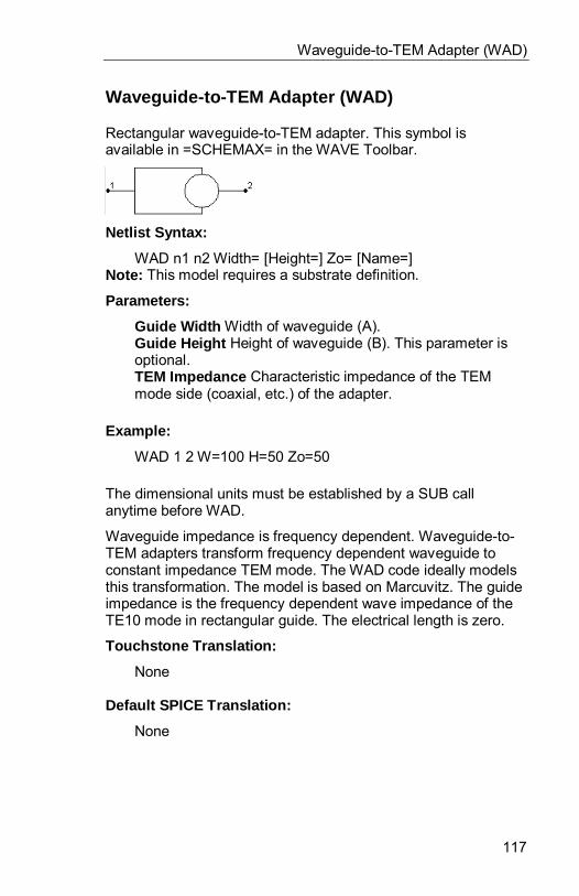
Waveguide-to-TEM Adapter (WAD)
117
Waveguide-to-TEM Adapter (WAD)
Rectangular waveguide-to-TEM adapter. This symbol isavailable in =SCHEMAX= in the WAVE Toolbar.
Netlist Syntax:
WAD n1 n2 Width= [Height=] Zo= [Name=]Note: This model requires a substrate definition.
Parameters:
Guide Width Width of waveguide (A).Guide Height Height of waveguide (B). This parameter isoptional.TEM Impedance Characteristic impedance of the TEMmode side (coaxial, etc.) of the adapter.
Example:
WAD 1 2 W=100 H=50 Zo=50
The dimensional units must be established by a SUB callanytime before WAD.
Waveguide impedance is frequency dependent. Waveguide-to-TEM adapters transform frequency dependent waveguide toconstant impedance TEM mode. The WAD code ideally modelsthis transformation. The model is based on Marcuvitz. The guideimpedance is the frequency dependent wave impedance of theTE10 mode in rectangular guide. The electrical length is zero.
Touchstone Translation:
None
Default SPICE Translation:
None
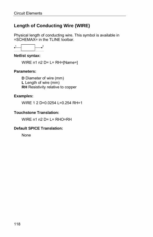
Circuit Elements
118
Length of Conducting Wire (WIRE)
Physical length of conducting wire. This symbol is available in=SCHEMAX= in the TLINE toolbar.
Netlist syntax:
WIRE n1 n2 D= L= RH=[Name=]
Parameters:
D Diameter of wire (mm)L Length of wire (mm)RH Resistivity relative to copper
Examples:
WIRE 1 2 D=0.0254 L=0.254 RH=1
Touchstone Translation:
WIRE n1 n2 D= L= RHO=RH
Default SPICE Translation:
None
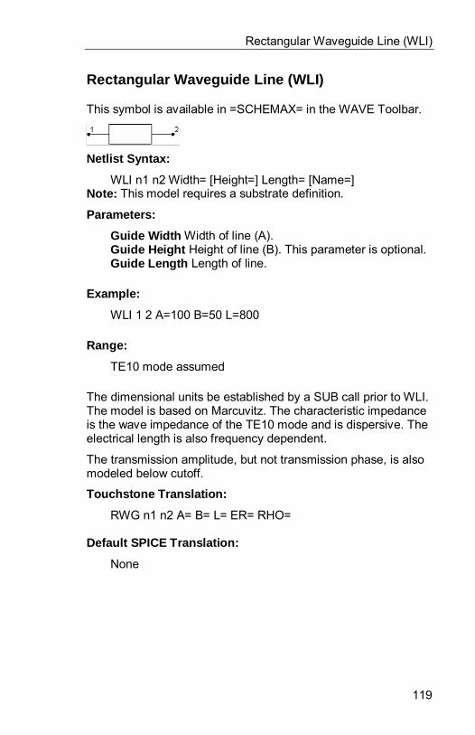
Rectangular Waveguide Line (WLI)
119
Rectangular Waveguide Line (WLI)
This symbol is available in =SCHEMAX= in the WAVE Toolbar.
Netlist Syntax:
WLI n1 n2 Width= [Height=] Length= [Name=]Note: This model requires a substrate definition.
Parameters:
Guide Width Width of line (A).Guide Height Height of line (B). This parameter is optional.Guide Length Length of line.
Example:
WLI 1 2 A=100 B=50 L=800
Range:
TE10 mode assumed
The dimensional units be established by a SUB call prior to WLI.The model is based on Marcuvitz. The characteristic impedanceis the wave impedance of the TE10 mode and is dispersive. Theelectrical length is also frequency dependent.
The transmission amplitude, but not transmission phase, is alsomodeled below cutoff.
Touchstone Translation:
RWG n1 n2 A= B= L= ER= RHO=
Default SPICE Translation:
None

Circuit Elements
120
Piezoelectric resonator (XTL)
This symbol is available in =SCHEMAX= in the LUMPEDToolbar.
Netlist Syntax:
XTL n1 n2 Rs= Lm= CM= CO= [Name=]
Parameters:
Series Resistance Series resistance in ohms.Motional Inductance Motional inductance in nanohenries.Motional Capacitance Motional Capacitance in picofarads.Parallel Capacitance Parallel Capacitance in picofarads.
Example:
XTL 1 2 Rs=26 Lm=4.97e6 Cm=.012741 Co=4.18
Touchstone Translation:
SRLC n1 n2 R=Rs L=Lm C=CmCAP n1 n2 C=Co
Default SPICE Translation:
.SUBCKT X$NAME 1 2R_series 1 3 RsL_motion 3 4 Lm nHC_motion 4 2 Cm pFC_parall 1 2 Co pF
.ENDS X$NAME
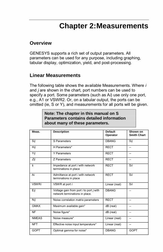
Chapter 2: Measurements
Overview
GENESYS supports a rich set of output parameters. Allparameters can be used for any purpose, including graphing,tabular display, optimization, yield, and post-processing.
Linear Measurements
The following table shows the available Measurements. Where iand j are shown in the chart, port numbers can be used tospecify a port. Some parameters (such as Ai) use only one port,e.g., A1 or VSWR2. Or, on a tabular output, the ports can beomitted (ie, S or Y), and measurements for all ports will be given.
Note: The chapter in this manual on SParameters contains detailed informationabout many of these parameters.
Meas. Description DefaultOperator
Shown onSmith Chart
Sij S Parameters DBANG Sij
Hij H Parameters* RECT --
Yij Y Parameters RECT --
Zij Z Parameters RECT --
Ii Impedance at port i with networkterminations in place
RECT Sii
Ai Admittance at port i with networkterminations in place
RECT Sii
VSWRi VSWR at port i Linear (real) Sii
Eij Voltage gain from port i to port j withnetwork terminations in place.
DBANG --
Nij Noise correlation matrix parameters RECT --
GMAX Maximum available gain* dB (real) --
NF Noise figure* dB (real) --
NMEAS Noise measure* Linear (real) --
NFT Effective noise input temperature* Linear (real) --
GOPT Optimal gamma for noise* DBANG GOPT
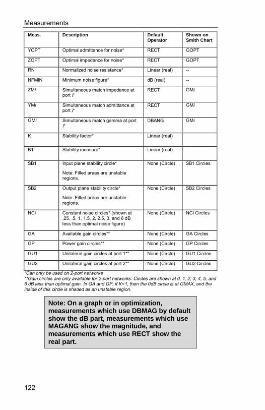
Measurements
122
Meas. Description DefaultOperator
Shown onSmith Chart
YOPT Optimal admittance for noise* RECT GOPT
ZOPT Optimal impedance for noise* RECT GOPT
RN Normalized noise resistance* Linear (real) --
NFMIN Minimum noise figure* dB (real) --
ZMi Simultaneous match impedance atport i*
RECT GMi
YMi Simultaneous match admittance atport i*
RECT GMi
GMi Simultaneous match gamma at porti*
DBANG GMi
K Stability factor* Linear (real)
B1 Stability measure* Linear (real)
SB1 Input plane stability circle*
Note: Filled areas are unstableregions.
None (Circle) SB1 Circles
SB2 Output plane stability circle*
Note: Filled areas are unstableregions.
None (Circle) SB2 Circles
NCI Constant noise circles* (shown at.25, .5, 1, 1.5, 2, 2.5, 3, and 6 dBless than optimal noise figure)
None (Circle) NCI Circles
GA Available gain circles** None (Circle) GA Circles
GP Power gain circles** None (Circle) GP Circles
GU1 Unilateral gain circles at port 1** None (Circle) GU1 Circles
GU2 Unilateral gain circles at port 2** None (Circle) GU2 Circles
*Can only be used on 2-port networks**Gain circles are only available for 2-port networks. Circles are shown at 0, 1, 2, 3, 4, 5, and6 dB less than optimal gain. In GA and GP, if K<1, then the 0dB circle is at GMAX, and theinside of this circle is shaded as an unstable region.
Note: On a graph or in optimization,measurements which use DBMAG by defaultshow the dB part, measurements which useMAGANG show the magnitude, andmeasurements which use RECT show thereal part.
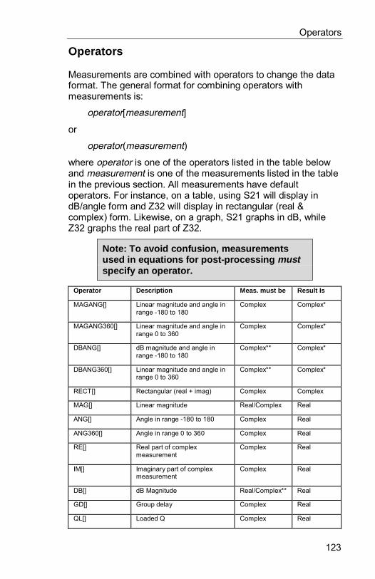
Operators
123
Operators
Measurements are combined with operators to change the dataformat. The general format for combining operators withmeasurements is:
operator[measurement]
or
operator(measurement)
where operator is one of the operators listed in the table belowand measurement is one of the measurements listed in the tablein the previous section. All measurements have defaultoperators. For instance, on a table, using S21 will display indB/angle form and Z32 will display in rectangular (real &complex) form. Likewise, on a graph, S21 graphs in dB, whileZ32 graphs the real part of Z32.
Note: To avoid confusion, measurementsused in equations for post-processing mustspecify an operator.
Operator Description Meas. must be Result Is
MAGANG[] Linear magnitude and angle inrange -180 to 180
Complex Complex*
MAGANG360[] Linear magnitude and angle inrange 0 to 360
Complex Complex*
DBANG[] dB magnitude and angle inrange -180 to 180
Complex** Complex*
DBANG360[] Linear magnitude and angle inrange 0 to 360
Complex** Complex*
RECT[] Rectangular (real + imag) Complex Complex
MAG[] Linear magnitude Real/Complex Real
ANG[] Angle in range -180 to 180 Complex Real
ANG360[] Angle in range 0 to 360 Complex Real
RE[] Real part of complexmeasurement
Complex Real
IM[] Imaginary part of complexmeasurement
Complex Real
DB[] dB Magnitude Real/Complex** Real
GD[] Group delay Complex Real
QL[] Loaded Q Complex Real
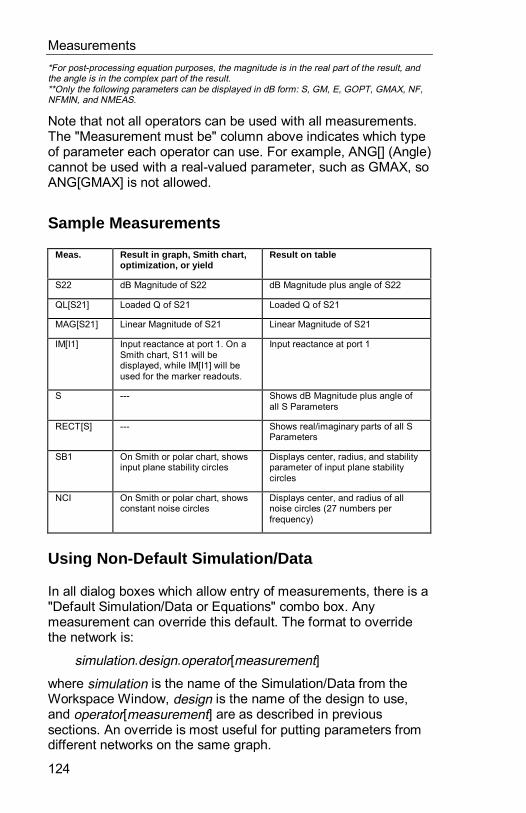
Measurements
124
*For post-processing equation purposes, the magnitude is in the real part of the result, andthe angle is in the complex part of the result.**Only the following parameters can be displayed in dB form: S, GM, E, GOPT, GMAX, NF,NFMIN, and NMEAS.
Note that not all operators can be used with all measurements.The "Measurement must be" column above indicates which typeof parameter each operator can use. For example, ANG[] (Angle)cannot be used with a real-valued parameter, such as GMAX, soANG[GMAX] is not allowed.
Sample Measurements
Meas. Result in graph, Smith chart,optimization, or yield
Result on table
S22 dB Magnitude of S22 dB Magnitude plus angle of S22
QL[S21] Loaded Q of S21 Loaded Q of S21
MAG[S21] Linear Magnitude of S21 Linear Magnitude of S21
IM[I1] Input reactance at port 1. On aSmith chart, S11 will bedisplayed, while IM[I1] will beused for the marker readouts.
Input reactance at port 1
S --- Shows dB Magnitude plus angle ofall S Parameters
RECT[S] --- Shows real/imaginary parts of all SParameters
SB1 On Smith or polar chart, showsinput plane stability circles
Displays center, radius, and stabilityparameter of input plane stabilitycircles
NCI On Smith or polar chart, showsconstant noise circles
Displays center, and radius of allnoise circles (27 numbers perfrequency)
Using Non-Default Simulation/Data
In all dialog boxes which allow entry of measurements, there is a"Default Simulation/Data or Equations" combo box. Anymeasurement can override this default. The format to overridethe network is:
simulation.design.operator[measurement]
where simulation is the name of the Simulation/Data from theWorkspace Window, design is the name of the design to use,and operator[measurement] are as described in previoussections. An override is most useful for putting parameters fromdifferent networks on the same graph.
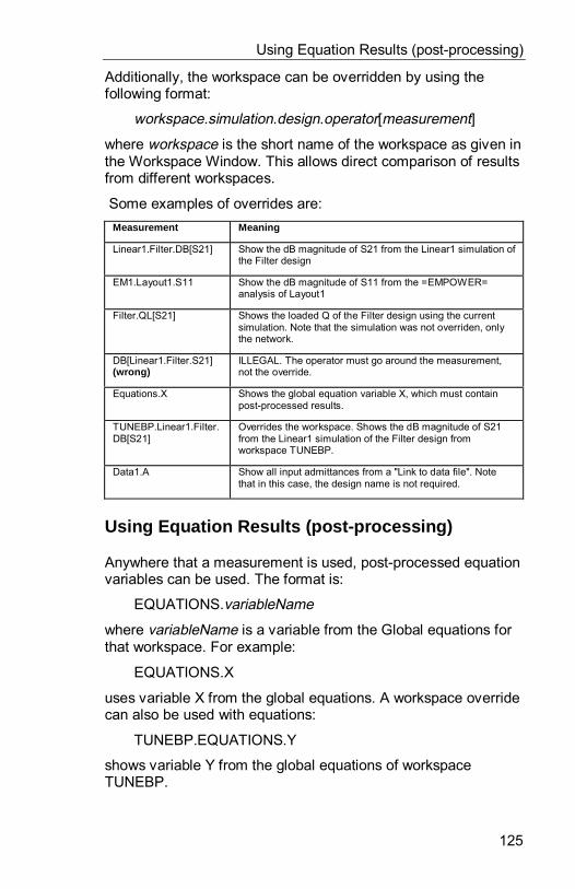
Using Equation Results (post-processing)
125
Additionally, the workspace can be overridden by using thefollowing format:
workspace.simulation.design.operator[measurement]
where workspace is the short name of the workspace as given inthe Workspace Window. This allows direct comparison of resultsfrom different workspaces.
Some examples of overrides are:Measurement Meaning
Linear1.Filter.DB[S21] Show the dB magnitude of S21 from the Linear1 simulation ofthe Filter design
EM1.Layout1.S11 Show the dB magnitude of S11 from the =EMPOWER=analysis of Layout1
Filter.QL[S21] Shows the loaded Q of the Filter design using the currentsimulation. Note that the simulation was not overriden, onlythe network.
DB[Linear1.Filter.S21](wrong)
ILLEGAL. The operator must go around the measurement,not the override.
Equations.X Shows the global equation variable X, which must containpost-processed results.
TUNEBP.Linear1.Filter.DB[S21]
Overrides the workspace. Shows the dB magnitude of S21from the Linear1 simulation of the Filter design fromworkspace TUNEBP.
Data1.A Show all input admittances from a "Link to data file". Notethat in this case, the design name is not required.
Using Equation Results (post-processing)
Anywhere that a measurement is used, post-processed equationvariables can be used. The format is:
EQUATIONS.variableName
where variableName is a variable from the Global equations forthat workspace. For example:
EQUATIONS.X
uses variable X from the global equations. A workspace overridecan also be used with equations:
TUNEBP.EQUATIONS.Y
shows variable Y from the global equations of workspaceTUNEBP.

Chapter 3: Equations
Statements
Each line in the EQUATIONS window must be in one of 5formats: assignment, REF, comment, IF, THEN, GOTO,FUNCTION, RETURN, or BASE. The formats are describedbelow.
Assignment
The assignment line assigns a value to a variable. Theassignment statement calculates the value of the expression andthen gives the value to the specified variable. Variables are notcase sensitive (for example, VAR and var are the same).Accuracy is IEEE double precision (about twelve digits). Theformat is:
Variablename = Expression
Examples:
X=2R=4*3/2^4*(9+8)Voltage=(2+R)*Current
Assignments can define a value to be a variable, which allowsthat variable to be tuned, optimized, or included in the MonteCarlo analysis. All variable names must start with an alphacharacter. The rest of the name may contain letters, numbersand the underscore ("_") character. The tune statement formatis:
VariableName = ?Value
Examples
X=?2Large_R=?3.54e+16
The tune statement must be a single assignment, not anexpression. Therefore, the following statement is illegal
X=?2+2 (WRONG!)
Equations
128
REF
This statement creates a reference to an expression. expressionmust be a simple variable, array element, or post-processeddata. This can make your equations faster and easier to write.The format of the reference statement is:
REF Variable = expression
Example:
B=5REF A=B 'A now points to BC=A+A 'C now equals 10A=C 'B (and, indirectly, A) now equals 10D=VECTOR(20)REF A=D[C] 'A points to D[10]A=3.14 'D[10] now equals 3.14.
Comment
A line is considered a comment if the first character in the line isan apostrophe ('). Any part of a line can be a comment andeverything after the apostrophe is ignored. The comment lineformat is:
'Comment
Example
'This line will be ignored.
LABEL
The label statement identifies a section of the EQUATIONSwindow for use in GOTO or IF THEN GOTO statements. Afterthe GOTO is executed, the statement following LABEL is thenext statement executed. If LABEL is the last statement in thewindow, the equations end after the GOTO. The format is:
LABEL Labelname
GOTO
This statement causes the EQUATION interpreter to jump in itscalculations to the statement following the corresponding LABELstatement. The format of the GOTO statement is:
GOTO Labelname
Statements
129
IF
This statement is perhaps the most powerful one included inGENESYS. This statement causes the following steps to occur.
1. The value of the expression is calculated. Any truecomparison results in a value of -1. For example, theexpression 1>0 gives a value of -1, while the expression0>1 gives a value of zero.
2. The value obtained in step one is compared to zero. Ifthe value is not zero, then the interpreter performs thestatement specified.
The format of the IF statement is:
IF expression THEN statement
Example:
IF Q>1000 THEN GOTO HIGHQRVal = 100GOTO DONELABEL HIGHQRVal = 500LABEL DONE
Warning: You cannot use IF/THEN with post-processed variables. Use the IFF and IFTRUEfunctions instead.
Since GENESYS uses approximate calculations (as anycomputer program must), round-off errors are inevitable. Thiscould cause a problem if you are using equality checks. If this isthe case, change
IF value = 5 THEN GOTO LABEL
to
IF ABS(value-5)<0.00001 THEN GOTO LABEL
or something similar. If you are using relational operators suchas greater than (>) or less than (<), this point does not need tobe considered.
FUNCTION
This statement is used to define functions. Functions take zeroor more parameters as input and return exactly one value asoutput. All variables used within a function are local; that is,
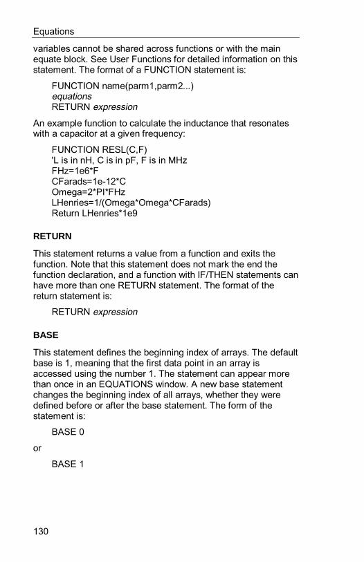
Equations
130
variables cannot be shared across functions or with the mainequate block. See User Functions for detailed information on thisstatement. The format of a FUNCTION statement is:
FUNCTION name(parm1,parm2...)equationsRETURN expression
An example function to calculate the inductance that resonateswith a capacitor at a given frequency:
FUNCTION RESL(C,F)'L is in nH, C is in pF, F is in MHzFHz=1e6*FCFarads=1e-12*COmega=2*PI*FHzLHenries=1/(Omega*Omega*CFarads)Return LHenries*1e9
RETURN
This statement returns a value from a function and exits thefunction. Note that this statement does not mark the end thefunction declaration, and a function with IF/THEN statements canhave more than one RETURN statement. The format of thereturn statement is:
RETURN expression
BASE
This statement defines the beginning index of arrays. The defaultbase is 1, meaning that the first data point in an array isaccessed using the number 1. The statement can appear morethan once in an EQUATIONS window. A new base statementchanges the beginning index of all arrays, whether they weredefined before or after the base statement. The form of thestatement is:
BASE 0
or
BASE 1
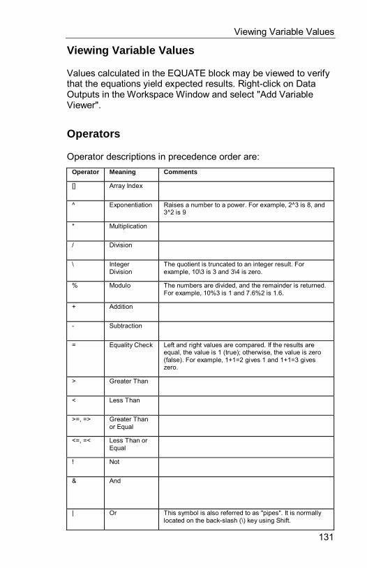
Viewing Variable Values
131
Viewing Variable Values
Values calculated in the EQUATE block may be viewed to verifythat the equations yield expected results. Right-click on DataOutputs in the Workspace Window and select "Add VariableViewer".
Operators
Operator descriptions in precedence order are:Operator Meaning Comments
[] Array Index
^ Exponentiation Raises a number to a power. For example, 2^3 is 8, and3^2 is 9
* Multiplication
/ Division
\ IntegerDivision
The quotient is truncated to an integer result. Forexample, 10\3 is 3 and 3\4 is zero.
% Modulo The numbers are divided, and the remainder is returned.For example, 10%3 is 1 and 7.6%2 is 1.6.
+ Addition
- Subtraction
= Equality Check Left and right values are compared. If the results areequal, the value is 1 (true); otherwise, the value is zero(false). For example, 1+1=2 gives 1 and 1+1=3 giveszero.
> Greater Than
< Less Than
>=, => Greater Thanor Equal
<=, =< Less Than orEqual
! Not
& And
| Or This symbol is also referred to as "pipes". It is normallylocated on the back-slash (\) key using Shift.
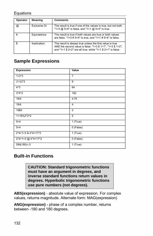
Equations
132
Operator Meaning Comments
@ Exclusive Or The result is true if one of the values is true, but not both."1=3 @ 5=4" is false, and "1=1 @ 5=4" is true.
# Equivalence The result is true if both values are true or both valuesare false. "1=3 # 5=4" is true, and "1=1 # 5=4" is false.
$ Implication The result is always true unless the first value is trueAND the second value is false. "1=3 $ 1=1", "1=3 $ 1=2",and "1=1 $ 2=2" are all true, while "1=1 $ 2=1" is false.
Sample Expressions
Expression Value
1+2*3 7
(1+2)*3 9
4^3 64
3*4^3 192
19/4 4.75
19\4 4
19$4 3
1+19%2*2^2 5
5>4 1 (True)
5<4 0 (False)
2*4>1+3 & 4*4<17^2 1 (True)
2*4>1+3 @ 4*4<17^2 0 (False)
SIN(180)<.5 1 (True)
Built-in Functions
CAUTION: Standard trigonometric functionsmust have an argument in degrees, andinverse standard functions return values indegrees. Hyperbolic trigonometric functionsuse pure numbers (not degrees).
ABS(express ion) - absolute value of expression. For complexvalues, returns magnitude. Alternate form: MAG(expression)
ANG(express ion) - phase of a complex number, returnsbetween -180 and 180 degrees.
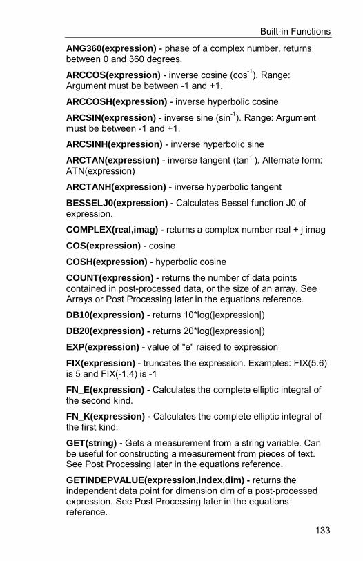
Built-in Functions
133
ANG360(express ion) - phase of a complex number, returnsbetween 0 and 360 degrees.
ARCCOS(express ion) - inverse cosine (cos-1). Range:Argument must be between -1 and +1.
ARCCOSH(express ion) - inverse hyperbolic cosine
ARCSIN(express ion) - inverse sine (sin-1). Range: Argumentmust be between -1 and +1.
ARCSINH(express ion) - inverse hyperbolic sine
ARCTAN(expression) - inverse tangent (tan-1). Alternate form:ATN(expression)
ARCTANH(expression) - inverse hyperbolic tangent
BESSELJ0(expression) - Calculates Bessel function J0 ofexpression.
COMPLEX(real,imag) - returns a complex number real + j imag
COS(expression) - cosine
COSH(expression) - hyperbolic cosine
COUNT(expression) - returns the number of data pointscontained in post-processed data, or the size of an array. SeeArrays or Post Processing later in the equations reference.
DB10(express ion) - returns 10*log(|expression|)
DB20(express ion) - returns 20*log(|expression|)
EXP(expression) - value of "e" raised to expression
FIX(express ion) - truncates the expression. Examples: FIX(5.6)is 5 and FIX(-1.4) is -1
FN_E(expression) - Calculates the complete elliptic integral ofthe second kind.
FN_K(express ion) - Calculates the complete elliptic integral ofthe first kind.
GET(string) - Gets a measurement from a string variable. Canbe useful for constructing a measurement from pieces of text.See Post Processing later in the equations reference.
GETINDEPVALUE(expression,index,dim) - returns theindependent data point for dimension dim of a post-processedexpression. See Post Processing later in the equationsreference.
Equations
134
Note: If the independent data is frequency,GETINDEPVALUE returns the values in Hz(not MHz).
GETVALUE(expression,index) - calculates and returns a valueof a post-processed expression. See Post Processing later in theequations reference.
GETVALUEAT(expression,indep) - calculates and returns avalue of a post-processed expression at a given independentvalue. Only works on 2 dimensional data (X vs.Y). See PostProcessing later in the equations reference.
Note: If the independent data is frequency,GETINDEPAT requires values in Hz (notMHz).
IFF(condition,trueValue,falseValue) - returns trueValue ifcondition is true, and falseValue if condition is false. Can beused with any data, including post-processed data.
IFTRUE(condition,trueValue) - returns trueValue if condition istrue, and zero if condition is false. Can be used with any data,including post-processed data.
IMAG(expression) - returns the imaginary part of a complexnumber. Alternate form: IM(expression)
INT(expression) - greatest integer less than or equal to theexpression Examples: INT(5.6) is 5 and INT(-1.4) is -2
LOG(expression) - base 10 logarithm
LN(expression) - natural logarithm
MATRIX(rows, columns) - Returns a 2-dimensional array ofsize rows x columns. See Arrays later in the equations reference.
MIN(expression) - Finds the minimum value of a post-processed expression.
MAX(express ion) - Finds the maximum value of a post-processed expression.
REAL(express ion) - returns the real part of a complex number.Alternate form: RE(expression)
RND - returns a pseudo-random number between zero and one
SIN(expression) - sine of the argument
Constants
135
SINH(expression) - hyperbolic sine
SQR(expression) - square root
TAN(expression) - tangent. Range: Argument must not be ±90,±3*90, etc.
TANH(expression) - hyperbolic tangent. Range: Same asTAN(expression)
VECTOR(expression) - returns a vector (array) of sizeexpression. See Arrays later in the equations reference.
Constants
Name Value
PI p, 3.14159265
_EPS0 8.854e-12
_ETA0 376.7343
_MU0 1.256637e-6
_VAIR c, 2.997925e8
_LN2 ln(2), 0.6931471805599
_EXP1 e, 2.718281828459
_RTOD Radians to degrees multiplier, 180/pi
_DTOR Degrees to radians multiplier, pi/180
Strings
String variables can be used in the equate block:
A="ABC" B="DEF" C=A+B
After this code, C="ABCDEF". Concatenation (+) is the onlyoperator currently defined for string variables, all otheroperations give undefined results.
If you create a model and want it to take a string variable as aparameter, put a ~ (tilde) in front of the parameter name in theModel Properties dialog box to indicate that it is a string.Furthermore, if the parameter starts with the word or is the word"~FILENAME", a browse button will be given to the user in theschematic part dialog box.
Equations
136
Arrays (Vectors and Matrices)
GENESYS allows you to create vectors and matrices in theequate block. Each element in a vector or matrix can hold anytype of data: real, complex, string, swept, or even a nested array.There are two functions which you can use to create arrays inyour equations:
VECTOR(x) - returns a vector (1-dimensional array) of x realzeros. Elements are accessed using square brackets and arebase one (numbering starts at one) by default:
A = VECTOR(3)A[1] = 1A[2] = 5A[3] = A[1] + A[2] 'A[3] now contains 6.
MATRIX(x,y) - returns a matrix (2-dimensional array) of x by yreal zeros. Elements are accessed using square brackets andare base one (numbering starts at one) by default:
B = MATRIX(2,2)B[1,1] = complex(1,3)B[1,2] = 3B[2,1] = 3B[2,2] = complex(1,-3)
Note for advanced users: Elements can also be accessedlinearly in row-column order, which can be useful in somesituations. Thus, the following equations work identically to theequations just given above:
B = MATRIX(2,2)B[1] = complex(1,3)B[2] = 3B[3] = 3B[4] = complex(1,-3)
GENESYS currently contains no special matrix mathematicaloperators. All operations simply work on each elementindividually. For example:
C=VECTOR(2)C[1]=5C[2]=-3.4D=VECTOR(2)D[1]=C[2]+3 'D[1] now equals -0.4D[2]=COMPLEX(5,6)E=C+D
Arrays (Vectors and Matrices)
137
E is now a two-element vector, E[1]=4.6, E[2]=-1.6 + j6.
Scalar/matrix combination operators also work. For instance,adding a complex number to a vector adds the complex numberto every element of the vector:
F=VECTOR(2)F[1]=1F[2]=2G=COMPLEX(3,4)H=F+G 'H[1]=4+j4, H[2]=5+j4
Matrices and vectors are safe; out of bounds access is alwayscaught. If an out-of-bounds index is used, the first element isused instead. If the variable being indexed is not an array, itsvalue is used instead.
If two matrices of different sizes are added, then the operation isonly performed up to the size of the smallest matrix. Theseoperations are performed as if the matrices were vectors; seethe example of linearly accessing a matrix as a vector above.
All operators and builtin functions will work properly on arrays,so, for example, taking the hyperbolic sine of matrix A usingSINH(A) will take the hyperbolic sine of each element of A. Also,arrays can be passed to user models and functions, so you cancreate a user model that takes a matrix or vector as a parameter.
Strings can be used in vectors, and the addition operator willwork. For example:
J=VECTOR(3)J[1]="One"J[2]="Two"J[3]="Three"K="Element "M=J+K 'M[1]="Element One", M[2]="Element Two", etc.
Note: Vectors and matrices are now baseone in GENESYS (first element is numberone). To use base zero, put the statement"BASE 0" on a blank line at the top of yourequations and at the top of any function.
To find out how many elements an array has, use the COUNTfunction:
N=VECTOR(71)P=COUNT(N) 'P=71
Equations
138
Q=MATRIX(100,75)R=COUNT(Q) 'R=7500
Post Processing
One of the more powerful features of the GENESYS equationblock is post-processing (sometimes referred to as OutputEquations). This allows you to perform calculations on the resultsof your analysis. These results can then be displayed, optimized,or even used in another design. For example:
Gain=Linear1.Filter.DB[S21]AddToGain = ?5TotalGain = Gain + AddToGain
This example takes the gain in dB, DB[S21], of the design "Filter"using the simulation setup in "Linear1" and places the result intothe variable "Gain". For a complete explanation of this syntax,see the Measurements section of this manual. Note that Gainnow contains swept data, DB[S21] vs. frequency. Next, thevariable AddToGain is added to each data point. The variableAddToGain can be tuned or optimized, which will directly affectthe value of TotalGain.
There are several important things to know about post-processed data:
y Any measurement described in the measurementssection of this manual is available for use in post-processing.
y To get simulation data, the expression must contain aperiod. For example A=DB[S21] will not work, butA=.DB[S21] will. This is most important if you takeadvantage of the USING statement (see below).
y To get simulation data, you must always use ameasurement operator. For example,A=Linear1.Filter.S21 will not work, butA=Linear1.Filter.DB[S21] will.
y Post-Processed variables can be mixed with "regular"variables as in the example above.
y Frequency-dependent post-processed variables can beused in part values. The data will besampled/interpolated/extracted as necessary, and theresulting part value may be different at each frequency.
Post Processing
139
For example, R=50+.1*FREQ can be used to create afrequency-dependent resistor.
y Post-Processed variables can be combined. Forexample, the statement"Difference=Linear1.Filter.DB[S21]-Measured.Data.DB[S21]" gives the difference betweenthe measured and the calculated DB[S21].
y For any operator or built-in function, swept data will belinearly interpolated if needed, and the resulting sweepwill contain all frequency points from both the measuredand the calculated data. In the item above, the differencevariable will contain all data points from both the linearanalysis and the measured data.
y All operators and built-in functions will work on post-processed data. For example, the statement"SineS=SIN(Linear1.FILTER.ANG[S21])" will take thesine of the phase of S21 at each data point.
y If the simulation data is itself a matrix, everything will stillwork fine. For example, the statement"Difference=Linear1.Filter.RECT[S]-Measured.Data.RECT[S]" will take the difference of all s-parameters. The Difference variable will now behave likean array (see the previous section), with the addition thatall operations will operate at all frequencies. Forexample, Difference[2,1] returns the difference of S21 atall frequencies.
y FREQ is a post-processed variable. For each frequencypoint, the value is that frequency. All frequencies are inMHz. Exception: In a user model, if the freq variable isused, the model is calculated once per frequency, andFREQ is just a normal number.
y Post-processed variables cannot be used in IF-THENstatements. For example, "IF .DB[S21]>5 THENGain=Gain+10" is not legal. Instead, you should use theIFF and IFTRUE functions. In this case, you can state"Gain=Gain+IFTRUE(.DB[S21]>5, 10)". This is becausethe equations are only calculated once (not at eachfrequency).
y All calculations are deferred until requested. This meansthat when any of the statements shown above areencountered, the required calculation is simply noted.Later, when the data is needed, the calculation is
Equations
140
performed. What does this mean to most users? Simplythat post-processed calculations are very fast, do notrequire a lot of memory overhead, and only calculatewhen necessary.
y The USING statement is a big convenience if you arewriting many expressions. With it, you only need tospecify the simulation/data and design once. The USINGstatement applies for all measurements specified after it,and it does not carry over into functions. For example:
USING Linear1.FILTERGain=.DB[S21]InputReflection=.DB[S11]OutputReflection=.DB[S22]Delay=.GD[S21]
Note: You must specify the period before themeasurement. This tells GENESYS that youare getting post-processed data. If you leaveout the period, you will get errors like"Unknown Variable S11".
Several functions in GENESYS are for use with post-processedcalculations:
Note: These are advanced functions whichare not required my most users. If you arenot sure if you need to use them, then youprobably don't.
COUNT(expression) - For post-processed data, this function willreturn the number of data points in the swept data. For example,if Linear1 is a linear simulation with 101 frequency points, thenCOUNT(Linear1.Sch.DB[S21]) is 101. This function is mostuseful if you want to loop post-processed data points withIF/THEN/GOTO Statements.
GET(string) - Gets a measurement from a string variable. Thestatements A=.DB[S21] and A=GET("DB[S21]") are identical.This statement exists so that you can pass a string containingthe name of a measurement into a function, allowing the functionto get the data.
GETINDEPVALUE(expression,index,dim) - returns theindependent data point for dimension dim of a post-processedexpression. Expression is the post-processed data, index is the
Logical Operators
141
point number, and dim is the independent dimension number touse. For normal frequency sweeps, dim should be 1. Forparameter sweeps with multiple independent sweeps, you mustuse dim to specify whether you want to get frequency (dim=1) orthe parameter (dim=2, or higher for nested parameter sweeps).
Note: If the independent data is frequency,GETINDEPVALUE returns the values in Hz(not MHz).
GETVALUE(expression,index) - calculates and returns a valueof a post-processed expression. This allows you to get the valueof an expression at a particular data point (index). This functionis most useful in combination with the COUNT function forlooping over values. Most users should not use this function,preferring the GETVALUEAT function instead. Note that thisfunction causes immediate calculation of the value, and thevalue it returns is not swept; it is the actual value of a particulardata point (real or imaginary). Advanced note: If the independentdata is multi-dimensional, then index can contain an arrayspecifying the index for each dimension.
GETVALUEAT(expression,indep) - calculates and returns avalue of a post-processed expression at a given independentvalue. For example, this allows you to get the value of anexpression at a particular frequency, such asQ=GETVALUEAT(.QL[S21],1e9) which gets the loaded Q of S21at 1 GHz. If no data has been calculated at 1 GHz, the data willbe interpolated or extrapolated as needed. While this function issomewhat slower than GETVALUE, it is much easier to usebecause you do not have to know the index of the point youwant. Note that this function causes immediate calculation of thevalue, and the value it returns is not swept; it is the actual valueof a particular data point (real or imaginary). Advanced note: Thisfunction only works on 2 dimensional data (X vs.Y).
Note: If the independent data is frequency,GETVALUEAT requires values in Hz (notMHz).
Logical Operators
The NOT, AND, OR, Exclusive-OR, EQV and IMP operators arecalled logical operators. They can be used to combine relational
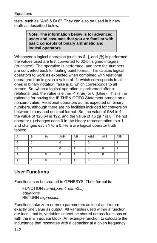
Equations
142
tests, such as "A<5 & B>6". They can also be used in binarymath as described below.
Note: The information below is for advancedusers and assumes that you are familiar withbasic concepts of binary arithmetic andlogical operators.
Whenever a logical operation (such as &, |, and @) is performed,the values used are first converted to 32-bit signed integers(truncated). The operation is performed, and then the numbersare converted back to floating point format. This causes logicaloperators to work as expected when combined with relationaloperators: true is given a value of -1, which corresponds to allones in binary notation; false is 0, which corresponds to allzeroes. So, when a logical operation is performed after arelational test, the value is either -1 (true) or 0 (false). This is therationale for having the IF THEN GOTO Statement branch on anonzero value. Relational operators act as expected on binarynumbers, although there are no facilities included for conversionbetween binary and decimal format. So, the value of 5&4 is 4,the value of 128|64 is 192, and the value of 15 @ 7 is 8. The notoperator (!) changes each 0 in the binary representation to a 1,and changes each 1 to a 0. Here are logical operator truthtables:
A B !A A&B A|B A@B A#B A$B
0 0 1 0 0 0 1 1
0 1 1 0 1 1 0 1
1 0 0 0 1 1 0 0
1 1 0 1 1 0 1 1
User Functions
Functions can be created in GENESYS. Their format is:
FUNCTION name(parm1,parm2...)equationsRETURN expression
Functions take zero or more parameters as input and returnexactly one value as output. All variables used within a functionare local; that is, variables cannot be shared across functions orwith the main equate block. An example function to calculate theinductance that resonates with a capacitor at a given frequency:
Calling Your FORTRAN/C/C++ DLLs
143
FUNCTION RESL(C,F)'L is in nH, C is in pF, F is in MHzFHz=1e6*FCFarads=1e-12*COmega=2*PI*FHzLHenries=1/(Omega*Omega*CFarads)Return LHenries*1e9
An example which uses this function is:
L=RESL(100,50) 'Find L to resonate 100pF at 50 MHz.
You could also type RESL(100,50) into a part in =SCHEMAX=.
Functions should go at the end of the global equations in yourworkspace. If you have functions you want to save permanently,save your workspace in the \EAGLE\MODEL directory. (Multiplefunctions can be placed in one file.) The functions will then beautomatically loaded when GENESYS is started.
For advanced uses, you can pass variables by reference, whichmeans that the function can directly modify the variables passedin. To pass a variable by reference, put the word BYREF in frontof the name. For example:
FUNCTION DOUBLE(BYREF X,BYREF Y)X=X*2Y=Y*2RETURN 0
Calling this function doubles the variables passed in. Forexample:
A=5B=6IGNORE=DOUBLE(A,B) 'After this call, A=10 andB=12.
Notice that all functions must return a value, even if you willignore it as in this case.
Calling Your FORTRAN/C/C++ DLLs
GENESYS has the capability to call programs you have written.The techniques for doing this are beyond the scope of thismanual. If you are interested in this capability, contactEagleware, and we will be happy to provide you with anapplication note with instructions.

Chapter 4: Units
Global Units
The units used in GENESYS are:Quantity Units
Resistance ohms
Inductance nH (nanohenries)
Capacitance pF (picofarads)
Conductance mhos (1/ohms or Siemens)
Frequency MHz (megahertz)
Delay ns (nanoseconds)
Angle Degrees
Physical Length, Width, Height mm (millimeters), or based on substrate
Note that physical length is unique:
y For parts which do not use a substrate, the units aremillimeters.
y For parts which use a substrate, the units are specifiedwith the substrate.
For layout dimensions, the units are specified in the Dimensionstab of the Layout Properties box with each layout.

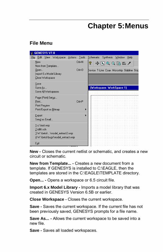
Chapter 5: Menus
File Menu
New - Closes the current netlist or schematic, and creates a newcircuit or schematic.
New from Template... - Creates a new document from atemplate. If GENESYS is installed to C:\EAGLE, then thetemplates are stored in the C:\EAGLE\TEMPLATE directory.
Open... - Opens a workspace or 6.5 circuit file.
Import 6.x Model Library - Imports a model library that wascreated in GENESYS Version 6.5B or earlier.
Close Workspace - Closes the current workspace.
Save - Saves the current workspace. If the current file has notbeen previously saved, GENESYS prompts for a file name.
Save As ... - Allows the current workspace to be saved into anew file.
Save - Saves all loaded workspaces.
Menus
148
Page (Print) Setup - Allows selection of printer and settings.
Print - Prints the current window.
Print Preview - Shows a preview of what the print command willprint.
Print/Export as Bitmap: Entire Screen - Prints the entirescreen, including any applications outside the GENESYSwindow.
Print/Export as Bitmap: Active Window - Prints only the activewindow/dialog box.
Export: S-Parameters - Exports a device data file from asimulation.
Export: SPICE File - Exports a SPICE file from the currentschematic.
Export: Touchstone File - Exports a Touchstone file from thecurrent schematic.
Export: =EMPOWER= Data Files - Exports all internal files foran =EMPOWER= simulation.
Export: DXF File - Exports a DXF File from the current layout.
Export: Gerber File - Exports a Gerber File from the currentlayout. Available formats are Gerber 274-D and 274-X.
Export: HPGL File - Exports a HPGL File from the currentlayout.
Export: ASCII Drill List - Exports an ASCII (Text) X-Y drill holelist from the current layout.
Export: Excellon (Gerber) Drill List - Exports an Excellon drillhole list from the current layout.
Send as Email... - Sends the current workspace as an emailattachment using your email program.
1...2...3...4 - Opens a recently used workspace file.
Exit - Exits GENESYS
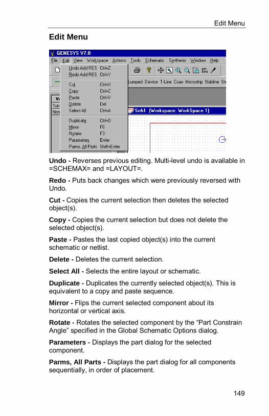
Edit Menu
149
Edit Menu
Undo - Reverses previous editing. Multi-level undo is available in=SCHEMAX= and =LAYOUT=.
Redo - Puts back changes which were previously reversed withUndo.
Cut - Copies the current selection then deletes the selectedobject(s).
Copy - Copies the current selection but does not delete theselected object(s).
Paste - Pastes the last copied object(s) into the currentschematic or netlist.
Delete - Deletes the current selection.
Select All - Selects the entire layout or schematic.
Duplicate - Duplicates the currently selected object(s). This isequivalent to a copy and paste sequence.
Mirror - Flips the current selected component about itshorizontal or vertical axis.
Rotate - Rotates the selected component by the “Part ConstrainAngle” specified in the Global Schematic Options dialog.
Parameters - Displays the part dialog for the selectedcomponent.
Parms, All Parts - Displays the part dialog for all componentssequentially, in order of placement.
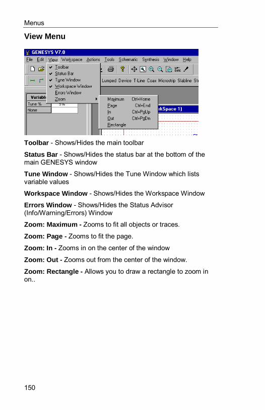
Menus
150
View Menu
Toolbar - Shows/Hides the main toolbar
Status Bar - Shows/Hides the status bar at the bottom of themain GENESYS window
Tune Window - Shows/Hides the Tune Window which listsvariable values
Workspace Window - Shows/Hides the Workspace Window
Errors Window - Shows/Hides the Status Advisor(Info/Warning/Errors) Window
Zoom: Maximum - Zooms to fit all objects or traces.
Zoom: Page - Zooms to fit the page.
Zoom: In - Zooms in on the center of the window
Zoom: Out - Zooms out from the center of the window.
Zoom: Rectangle - Allows you to draw a rectangle to zoom inon..
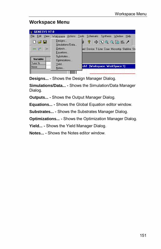
Workspace Menu
151
Workspace Menu
Designs... - Shows the Design Manager Dialog.
Simulations/Data... - Shows the Simulation/Data ManagerDialog.
Outputs... - Shows the Output Manager Dialog.
Equations... - Shows the Global Equation editor window.
Substrates... - Shows the Substrates Manager Dialog.
Optimizations... - Shows the Optimization Manager Dialog.
Yield... - Shows the Yield Manager Dialog.
Notes... - Shows the Notes editor window.
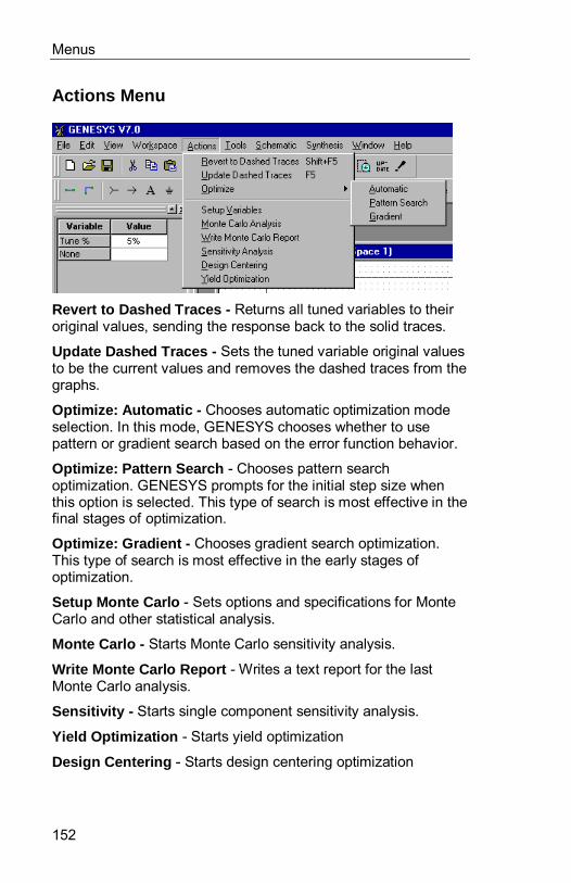
Menus
152
Actions Menu
Revert to Dashed Traces - Returns all tuned variables to theiroriginal values, sending the response back to the solid traces.
Update Dashed Traces - Sets the tuned variable original valuesto be the current values and removes the dashed traces from thegraphs.
Optimize: Automatic - Chooses automatic optimization modeselection. In this mode, GENESYS chooses whether to usepattern or gradient search based on the error function behavior.
Optimize: Pattern Search - Chooses pattern searchoptimization. GENESYS prompts for the initial step size whenthis option is selected. This type of search is most effective in thefinal stages of optimization.
Optimize: Gradient - Chooses gradient search optimization.This type of search is most effective in the early stages ofoptimization.
Setup Monte Carlo - Sets options and specifications for MonteCarlo and other statistical analysis.
Monte Carlo - Starts Monte Carlo sensitivity analysis.
Write Monte Carlo Report - Writes a text report for the lastMonte Carlo analysis.
Sensitivity - Starts single component sensitivity analysis.
Yield Optimization - Starts yield optimization
Design Centering - Starts design centering optimization

Tools Menu
153
Tools Menu
User Toolbars - Not currently available. Instead, place anexisting symbol on your schematic and change its model.
Footprint Editor: New Footprint... - Creates a new =LAYOUT=component footprint.
Footprint Editor: Load Footprint... - Edits an existing=LAYOUT= component footprint.
Footprint Editor: Merge Footprint... - Merges an existing=LAYOUT= component footprint into the current footprint editorwindow.
Footprint Editor: Save Footprint... - Saves the footprint in theactive footprint editor.
Footprint Editor: Modify Footprint Library... - Allows renamingor deletion of footprints in footprint libraries.

Menus
154
Schematic Menu
Make Tunable - Forces all components to betunable/optimizable by adding question marks to the first value ofeach component. This only adds question marks to part valueswith a numerical value. In other words, if a variable is used for aparticular value, it will not be made tunable.
Properties - Shows the the Schematic Properties dialog box.
Renumber Nodes - Renumbers all nodes. This is primarilyuseful before exporting a SPICE file.
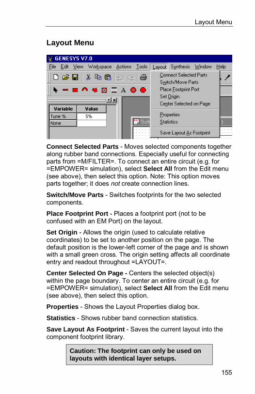
Layout Menu
155
Layout Menu
Connect Selected Parts - Moves selected components togetheralong rubber band connections. Especially useful for connectingparts from =M/FILTER=. To connect an entire circuit (e.g. for=EMPOWER= simulation), select Select All from the Edit menu(see above), then select this option. Note: This option movesparts together; it does not create connection lines.
Switch/Move Parts - Switches footprints for the two selectedcomponents.
Place Footprint Port - Places a footprint port (not to beconfused with an EM Port) on the layout.
Set Origin - Allows the origin (used to calculate relativecoordinates) to be set to another position on the page. Thedefault position is the lower-left corner of the page and is shownwith a small green cross. The origin setting affects all coordinateentry and readout throughout =LAYOUT=.
Center Selected On Page - Centers the selected object(s)within the page boundary. To center an entire circuit (e.g. for=EMPOWER= simulation), select Select All from the Edit menu(see above), then select this option.
Properties - Shows the Layout Properties dialog box.
Statistics - Shows rubber band connection statistics.
Save Layout As Footprint - Saves the current layout into thecomponent footprint library.
Caution: The footprint can only be used onlayouts with identical layer setups.
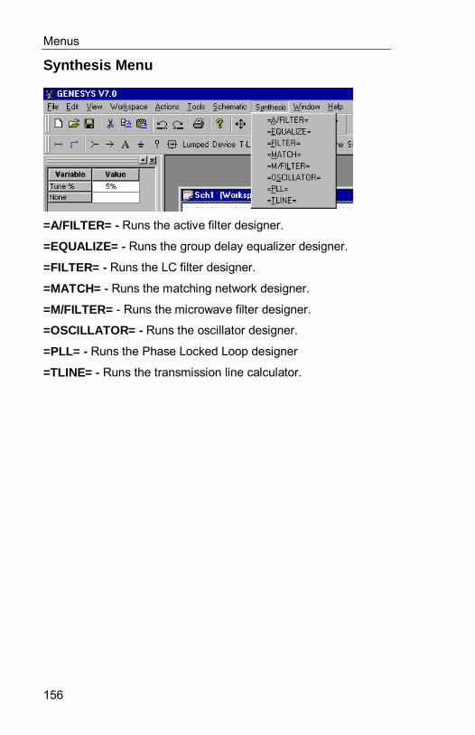
Menus
156
Synthesis Menu
=A/FILTER= - Runs the active filter designer.
=EQUALIZE= - Runs the group delay equalizer designer.
=FILTER= - Runs the LC filter designer.
=MATCH= - Runs the matching network designer.
=M/FILTER= - Runs the microwave filter designer.
=OSCILLATOR= - Runs the oscillator designer.
=PLL= - Runs the Phase Locked Loop designer
=TLINE= - Runs the transmission line calculator.
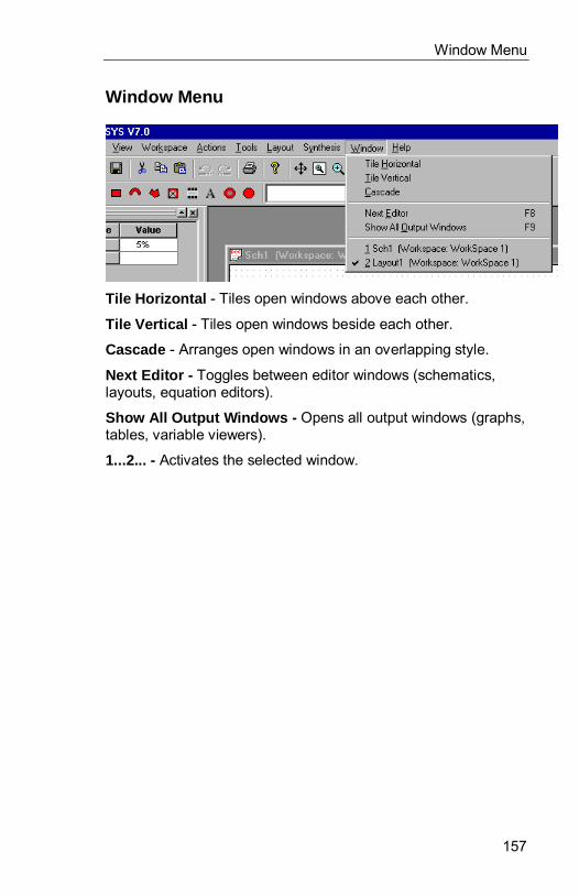
Window Menu
157
Window Menu
Tile Horizontal - Tiles open windows above each other.
Tile Vertical - Tiles open windows beside each other.
Cascade - Arranges open windows in an overlapping style.
Next Editor - Toggles between editor windows (schematics,layouts, equation editors).
Show All Output Windows - Opens all output windows (graphs,tables, variable viewers).
1...2... - Activates the selected window.

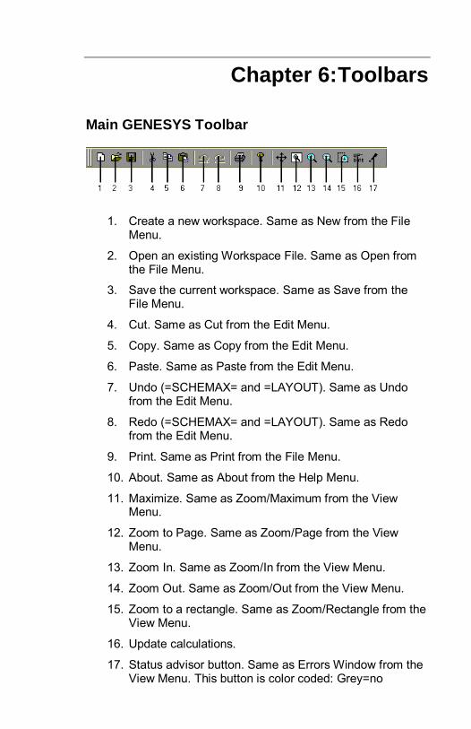
Chapter 6: Toolbars
Main GENESYS Toolbar
1. Create a new workspace. Same as New from the FileMenu.
2. Open an existing Workspace File. Same as Open fromthe File Menu.
3. Save the current workspace. Same as Save from theFile Menu.
4. Cut. Same as Cut from the Edit Menu.
5. Copy. Same as Copy from the Edit Menu.
6. Paste. Same as Paste from the Edit Menu.
7. Undo (=SCHEMAX= and =LAYOUT). Same as Undofrom the Edit Menu.
8. Redo (=SCHEMAX= and =LAYOUT). Same as Redofrom the Edit Menu.
9. Print. Same as Print from the File Menu.
10. About. Same as About from the Help Menu.
11. Maximize. Same as Zoom/Maximum from the ViewMenu.
12. Zoom to Page. Same as Zoom/Page from the ViewMenu.
13. Zoom In. Same as Zoom/In from the View Menu.
14. Zoom Out. Same as Zoom/Out from the View Menu.
15. Zoom to a rectangle. Same as Zoom/Rectangle from theView Menu.
16. Update calculations.
17. Status advisor button. Same as Errors Window from theView Menu. This button is color coded: Grey=no
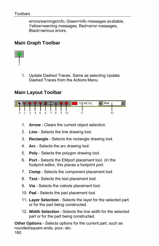
Toolbars
160
errors/warnings/info, Green=info messages available,Yellow=warning messages, Red=error messages,Black=serious errors.
Main Graph Toolbar
1. Update Dashed Traces. Same as selecting UpdateDashed Traces from the Actions Menu.
Main Layout Toolbar
1. Arrow - Clears the current object selection.
2. Line - Selects the line drawing tool.
3. Rectangle - Selects the rectangle drawing tool.
4. Arc - Selects the arc drawing tool.
5. Poly - Selects the polygon drawing tool.
6. Port - Selects the EMport placement tool. (In thefootprint editor, this places a footprint port.
7. Comp - Selects the component placement tool.
8. Text - Selects the text placement tool.
9. Via - Selects the viahole placement tool.
10. Pad - Selects the pad placement tool.
11. Layer Selection - Selects the layer for the selected partor for the part being constructed.
12. Width Selection - Selects the line width for the selectedpart or for the part being constructed.
Other Options - Selects options for the current part, such asrounded/square ends, pour, etc.
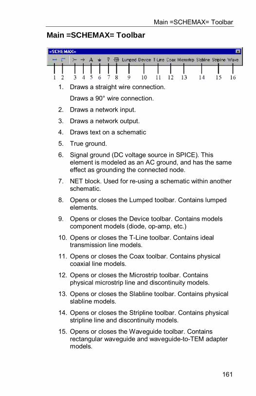
Main =SCHEMAX= Toolbar
161
Main =SCHEMAX= Toolbar
1. Draws a straight wire connection.
Draws a 90° wire connection.
2. Draws a network input.
3. Draws a network output.
4. Draws text on a schematic
5. True ground.
6. Signal ground (DC voltage source in SPICE). Thiselement is modeled as an AC ground, and has the sameeffect as grounding the connected node.
7. NET block. Used for re-using a schematic within anotherschematic.
8. Opens or closes the Lumped toolbar. Contains lumpedelements.
9. Opens or closes the Device toolbar. Contains modelscomponent models (diode, op-amp, etc.)
10. Opens or closes the T-Line toolbar. Contains idealtransmission line models.
11. Opens or closes the Coax toolbar. Contains physicalcoaxial line models.
12. Opens or closes the Microstrip toolbar. Containsphysical microstrip line and discontinuity models.
13. Opens or closes the Slabline toolbar. Contains physicalslabline models.
14. Opens or closes the Stripline toolbar. Contains physicalstripline line and discontinuity models.
15. Opens or closes the Waveguide toolbar. Containsrectangular waveguide and waveguide-to-TEM adaptermodels.
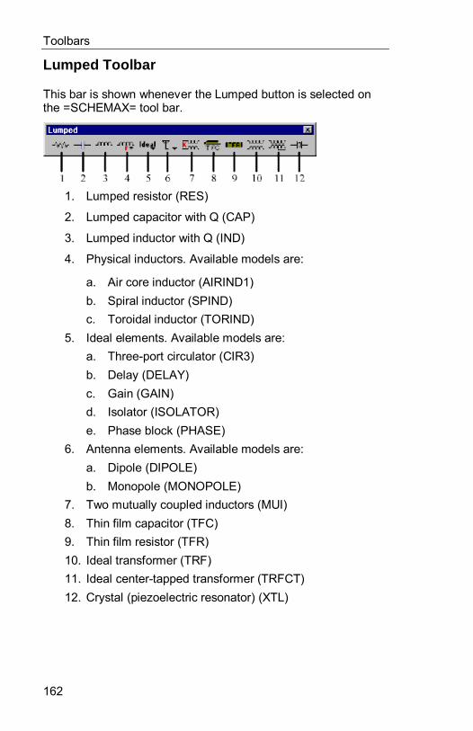
Toolbars
162
Lumped Toolbar
This bar is shown whenever the Lumped button is selected onthe =SCHEMAX= tool bar.
1. Lumped resistor (RES)
2. Lumped capacitor with Q (CAP)
3. Lumped inductor with Q (IND)
4. Physical inductors. Available models are:
a. Air core inductor (AIRIND1)b. Spiral inductor (SPIND)c. Toroidal inductor (TORIND)
5. Ideal elements. Available models are:a. Three-port circulator (CIR3)b. Delay (DELAY)c. Gain (GAIN)d. Isolator (ISOLATOR)e. Phase block (PHASE)
6. Antenna elements. Available models are:a. Dipole (DIPOLE)b. Monopole (MONOPOLE)
7. Two mutually coupled inductors (MUI)8. Thin film capacitor (TFC)9. Thin film resistor (TFR)10. Ideal transformer (TRF)11. Ideal center-tapped transformer (TRFCT)12. Crystal (piezoelectric resonator) (XTL)
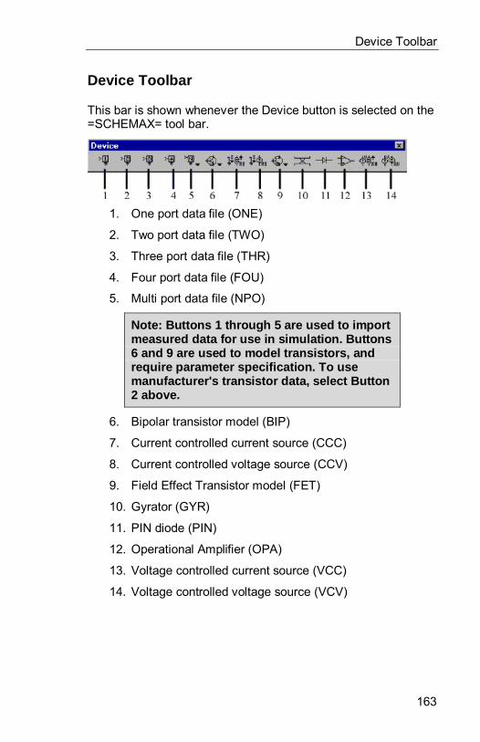
Device Toolbar
163
Device Toolbar
This bar is shown whenever the Device button is selected on the=SCHEMAX= tool bar.
1. One port data file (ONE)
2. Two port data file (TWO)
3. Three port data file (THR)
4. Four port data file (FOU)
5. Multi port data file (NPO)
Note: Buttons 1 through 5 are used to importmeasured data for use in simulation. Buttons6 and 9 are used to model transistors, andrequire parameter specification. To usemanufacturer's transistor data, select Button2 above.
6. Bipolar transistor model (BIP)
7. Current controlled current source (CCC)
8. Current controlled voltage source (CCV)
9. Field Effect Transistor model (FET)
10. Gyrator (GYR)
11. PIN diode (PIN)
12. Operational Amplifier (OPA)
13. Voltage controlled current source (VCC)
14. Voltage controlled voltage source (VCV)
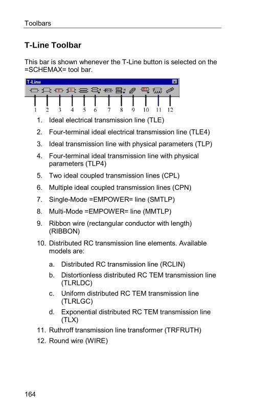
Toolbars
164
T-Line Toolbar
This bar is shown whenever the T-Line button is selected on the=SCHEMAX= tool bar.
1. Ideal electrical transmission line (TLE)
2. Four-terminal ideal electrical transmission line (TLE4)
3. Ideal transmission line with physical parameters (TLP)
4. Four-terminal ideal transmission line with physicalparameters (TLP4)
5. Two ideal coupled transmission lines (CPL)
6. Multiple ideal coupled transmission lines (CPN)
7. Single-Mode =EMPOWER= line (SMTLP)
8. Multi-Mode =EMPOWER= line (MMTLP)
9. Ribbon wire (rectangular conductor with length)(RIBBON)
10. Distributed RC transmission line elements. Availablemodels are:
a. Distributed RC transmission line (RCLIN)b. Distortionless distributed RC TEM transmission line
(TLRLDC)c. Uniform distributed RC TEM transmission line
(TLRLGC)d. Exponential distributed RC TEM transmission line
(TLX)11. Ruthroff transmission line transformer (TRFRUTH)12. Round wire (WIRE)
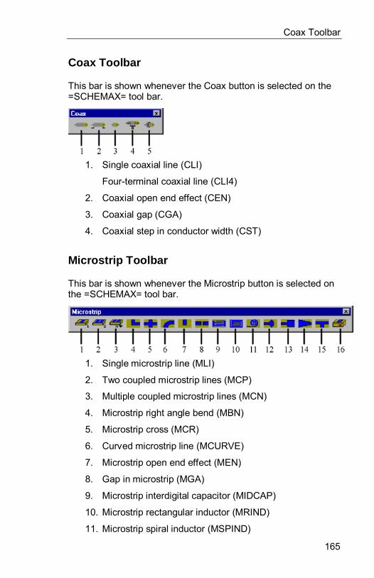
Coax Toolbar
165
Coax Toolbar
This bar is shown whenever the Coax button is selected on the=SCHEMAX= tool bar.
1. Single coaxial line (CLI)
Four-terminal coaxial line (CLI4)
2. Coaxial open end effect (CEN)
3. Coaxial gap (CGA)
4. Coaxial step in conductor width (CST)
Microstrip Toolbar
This bar is shown whenever the Microstrip button is selected onthe =SCHEMAX= tool bar.
1. Single microstrip line (MLI)
2. Two coupled microstrip lines (MCP)
3. Multiple coupled microstrip lines (MCN)
4. Microstrip right angle bend (MBN)
5. Microstrip cross (MCR)
6. Curved microstrip line (MCURVE)
7. Microstrip open end effect (MEN)
8. Gap in microstrip (MGA)
9. Microstrip interdigital capacitor (MIDCAP)
10. Microstrip rectangular inductor (MRIND)
11. Microstrip spiral inductor (MSPIND)
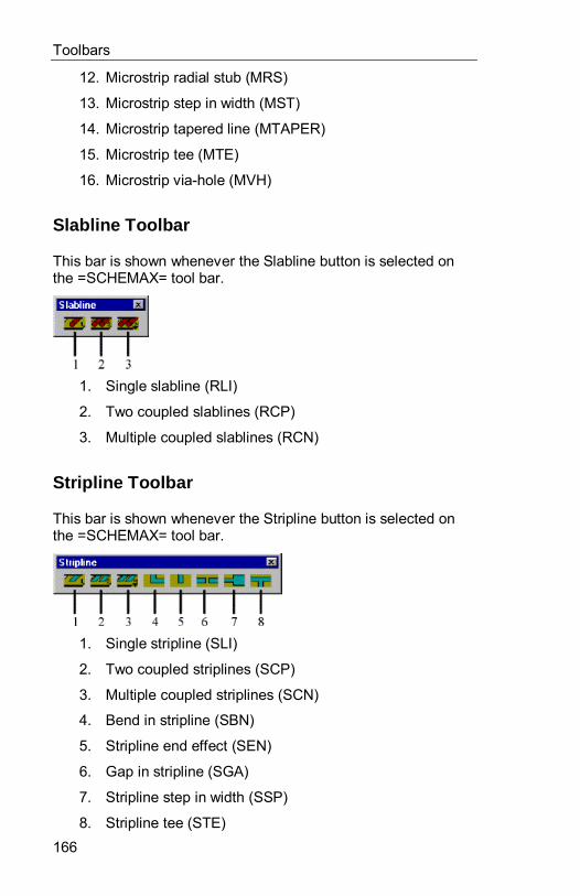
Toolbars
166
12. Microstrip radial stub (MRS)
13. Microstrip step in width (MST)
14. Microstrip tapered line (MTAPER)
15. Microstrip tee (MTE)
16. Microstrip via-hole (MVH)
Slabline Toolbar
This bar is shown whenever the Slabline button is selected onthe =SCHEMAX= tool bar.
1. Single slabline (RLI)
2. Two coupled slablines (RCP)
3. Multiple coupled slablines (RCN)
Stripline Toolbar
This bar is shown whenever the Stripline button is selected onthe =SCHEMAX= tool bar.
1. Single stripline (SLI)
2. Two coupled striplines (SCP)
3. Multiple coupled striplines (SCN)
4. Bend in stripline (SBN)
5. Stripline end effect (SEN)
6. Gap in stripline (SGA)
7. Stripline step in width (SSP)
8. Stripline tee (STE)

Waveguide Toolbar
167
Waveguide Toolbar
This bar is shown whenever the Wave button is selected on the=SCHEMAX= tool bar.
1. Rectangular waveguide-to-TEM adapter (WAD)
2. Rectangular waveguide (WLI)

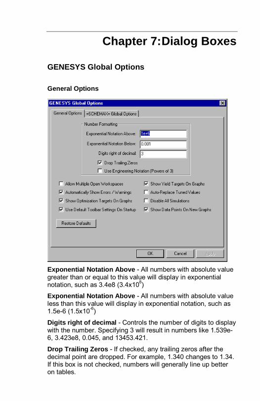
Chapter 7: Dialog Boxes
GENESYS Global Options
General Options
Exponential Notation Above - All numbers with absolute valuegreater than or equal to this value will display in exponentialnotation, such as 3.4e8 (3.4x10⁸)
Exponential Notation Above - All numbers with absolute valueless than this value will display in exponential notation, such as1.5e-6 (1.5x10⁻⁶)
Digits right of decimal - Controls the number of digits to displaywith the number. Specifying 3 will result in numbers like 1.539e-6, 3.423e8, 0.045, and 13453.421.
Drop Trailing Zeros - If checked, any trailing zeros after thedecimal point are dropped. For example, 1.340 changes to 1.34.If this box is not checked, numbers will generally line up betteron tables.
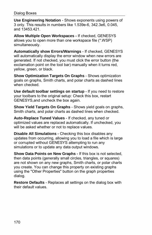
Dialog Boxes
170
Use Engineering Notation - Shows exponents using powers of3 only. This results in numbers like 1.539e-6, 342.3e6, 0.045,and 13453.421.
Allow Multiple Open Wo rkspaces - If checked, GENESYSallows you to open more than one workspace file (*.WSP)simultaneously.
Automatically show Errors/Warnings - If checked, GENESYSwill automatically display the error window when new errors aregenerated. If not checked, you must click the error button (theexclamation point on the tool bar) manually when it turns red,yellow, green, or black.
Show Optimization Targets On Graphs - Shows optimizationgoals on graphs, Smith charts, and polar charts as dashed lineswhen checked.
Use default toolbar settings on startup - If you need to restoreyour toolbars to the original setup: Check this box, restartGENESYS,and uncheck the box again.
Show Yield Targets On Graphs - Shows yield goals on graphs,Smith charts, and polar charts as dashed lines when checked.
Auto-Replace Tuned Values - If checked, any tuned oroptimized values are replaced automatically. If unchecked, youwill be asked whether or not to replace values.
Disable All Simulations - Checking this box disables anyupdates from occurring, allowing you to load a file which is largeor corrupted without GENESYS attempting to run anysimulations or to update any data output windows.
Show Data Points on New Graphs - If this box is not selected,then data points (generally small circles, triangles, or squares)are not shown on any new graphs, Smith charts, or polar chartsyou create. You can change this property on existing graphsusing the "Other Properties" button on the graph propertiesdialog.
Restore Defaults - Replaces all settings on the dialog box withtheir default values.
GENESYS Global Options
171
=SCHEMAX= Global Options
Zoom In (Radio Button) - Sets the right or center mouse buttonfunction. If this button is selected, clicking the mouse button onthe schematic will zoom in on the mouse pointer location.
Zoom Out (Radio Button) - Sets the right or center mousebutton function. If this button is selected, clicking the mousebutton on the schematic will zoom out from the mouse pointerlocation.
Show Part Dialog Box (Radio Button) - Sets the right or centermouse button function. If this button is selected, clicking themouse button on a schematic object will open the dialog box forthat component.
Part Constrain Angle - Specifies the rotation snap angle forschematic parts.
Junction Circle Size - Sets the drawing size for node circles onthe schematic.
Automatically display part dialog.... (Checkbox) -Automatically displays the component’s associated dialogwhenever a component is placed on the schematic page.

Dialog Boxes
172
Show grid (Checkbox) - Displays the schematic backgroundgrid.
Show node zones (Checkbox) - Shows node circles on eachcomponent.
Use long parts by default (Checkbox) - Short parts are usuallycreated by holding SHIFT while placing a component on theschematic. If this option is selected, short parts are alwaysplaced, unless SHIFT is held down.
Allow multiple parts to be placed... (Checkbox) - Forces=SCHEMAX= to remain in the part placement mode untilESCAPE is pressed, or another action is selected.
Show node numbers (Checkbox) - Shows node numbers onthe schematic at each component connection.
Show SPICE Details in Part Dialogs - If you will be exporting aspice file, be sure to check this dialog box so that you can seeand override spice translations in the Schematic dialogs.
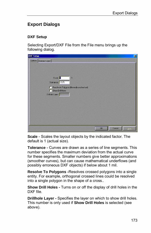
Export Dialogs
173
Export Dialogs
DXF Setup
Selecting Export/DXF File from the File menu brings up thefollowing dialog.
Scale - Scales the layout objects by the indicated factor. Thedefault is 1 (actual size).
Tolerance - Curves are drawn as a series of line segments. Thisnumber specifies the maximum deviation from the actual curvefor these segments. Smaller numbers give better approximations(smoother curves), but can cause mathematical underflows (andpossibly erroneous DXF objects) if below about 1 mil.
Resolve To Polygons - Resolves crossed polygons into a singleentity. For example, orthogonal crossed lines could be resolvedinto a single polygon in the shape of a cross..
Show Drill Holes - Turns on or off the display of drill holes in theDXF file.
Drillhole Layer - Specifies the layer on which to show drill holes.This number is only used if Show Drill Holes is selected (seeabove).
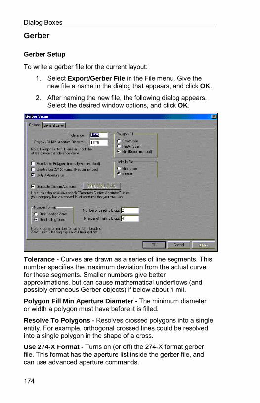
Dialog Boxes
174
Gerber
Gerber Setup
To write a gerber file for the current layout:
1. Select Export/Gerber File in the File menu. Give thenew file a name in the dialog that appears, and click OK.
2. After naming the new file, the following dialog appears.Select the desired window options, and click OK.
Tolerance - Curves are drawn as a series of line segments. Thisnumber specifies the maximum deviation from the actual curvefor these segments. Smaller numbers give betterapproximations, but can cause mathematical underflows (andpossibly erroneous Gerber objects) if below about 1 mil.
Polygon Fill Min Aperture Diameter - The minimum diameteror width a polygon must have before it is filled.
Resolve To Polygons - Resolves crossed polygons into a singleentity. For example, orthogonal crossed lines could be resolvedinto a single polygon in the shape of a cross.
Use 274-X Format - Turns on (or off) the 274-X format gerberfile. This format has the aperture list inside the gerber file, andcan use advanced aperture commands.
Export Dialogs
175
Output Aperture List - Causes =LAYOUT= to write an aperturelist. This is only valid for non-274-X formats, since the aperturelist is embedded for 274-X files.
Polygon Fill - Specifies the polygon fill algorithm to be used:
SmartScan - Attempts to minimize file size, but does notwork for all possiblitiesRaster Scan - Uses a very reliable algorithm which createsrelatively large filesMix - Automatically switches between SmartScan andRaster Scan
Units in File- Specifies the units to use inside the gerber file.The available options are millimeters and mils.
Generate Custom Apertures - Allows you to specify aperturesfor =LAYOUT= to use within the gerber file. Selecting thischeckbox makes the “Edit Default.APL” button available (seebelow). Why use custom apertures?
Edit DEFAULT.APL Button - Opens the Custom Aperture Listdialog. You can edit the list and add your own custom apertures.
Number Format - Specifies the type of numbering used withinthe gerber file. Available options are:
Omit Leading Zeros - Uses trailing zeros to fillremaining pl aceholders if not enough non-zero digitsexist.Omit Trailing Zeros - Uses leading zeros to fill remainingplaceholders if not enough non-zero digits exist.
Number of Leading Digits - Specifies the number of digitsbefore the decimal to use within the gerber file.
Number of Trailing Digits - Specifies the number of digits afterthe decimal to use within the gerber file.
Editing an Aperture List
Why use custom apertures?
If Generate Custom Apertures is selected in the Gerber Setupdialog, the “Edit DEFAULT.APL” button becomes available.Clicking this button brings up the following dialog. The dialogobjects are described below. You can also click on the followingimage for specific information.
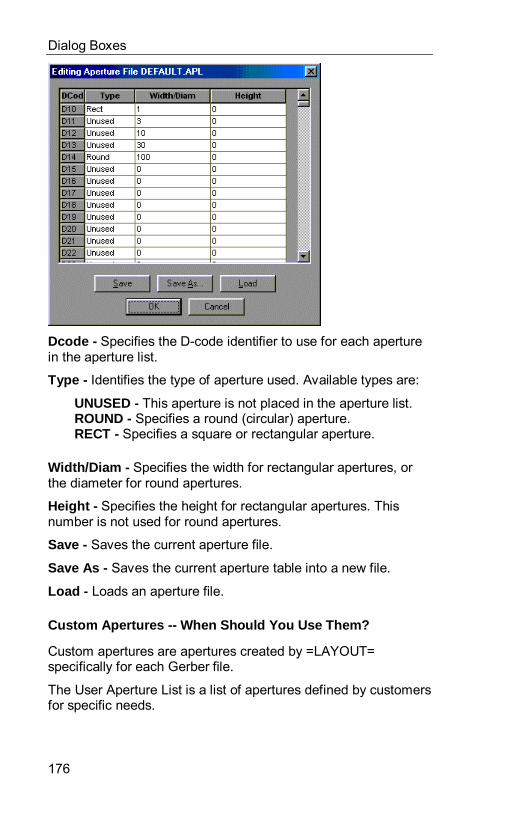
Dialog Boxes
176
Dcode - Specifies the D-code identifier to use for each aperturein the aperture list.
Type - Identifies the type of aperture used. Available types are:
UNUSED - This aperture is not placed in the aperture list.ROUND - Specifies a round (circular) aperture.RECT - Specifies a square or rectangular aperture.
Width/Diam - Specifies the width for rectangular apertures, orthe diameter for round apertures.
Height - Specifies the height for rectangular apertures. Thisnumber is not used for round apertures.
Save - Saves the current aperture file.
Save As - Saves the current aperture table into a new file.
Load - Loads an aperture file.
Custom Apertures -- When Should You Use Them?
Custom apertures are apertures created by =LAYOUT=specifically for each Gerber file.
The User Aperture List is a list of apertures defined by customersfor specific needs.

Export Dialogs
177
Generally, user apertures should only be used if your companyhas a standard set of apertures that Gerber exports mustconform to. Otherwise, custom apertures should be used.
=LAYOUT= has a built in optimization routine that selects thebest list of apertures for efficient polygon fills and flashes. Thesecustom apertures result in the smallest possible Gerber files,whereas a user list can give very inefficient, incorrect, and largefiles.
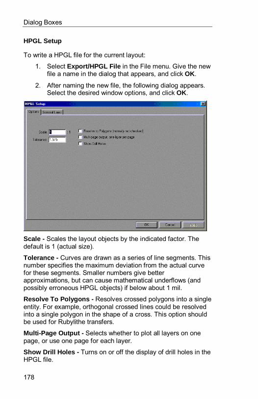
Dialog Boxes
178
HPGL Setup
To write a HPGL file for the current layout:
1. Select Export/HPGL File in the File menu. Give the newfile a name in the dialog that appears, and click OK.
2. After naming the new file, the following dialog appears.Select the desired window options, and click OK.
Scale - Scales the layout objects by the indicated factor. Thedefault is 1 (actual size).
Tolerance - Curves are drawn as a series of line segments. Thisnumber specifies the maximum deviation from the actual curvefor these segments. Smaller numbers give betterapproximations, but can cause mathematical underflows (andpossibly erroneous HPGL objects) if below about 1 mil.
Resolve To Polygons - Resolves crossed polygons into a singleentity. For example, orthogonal crossed lines could be resolvedinto a single polygon in the shape of a cross. This option shouldbe used for Rubylithe transfers.
Multi-Page Output - Selects whether to plot all layers on onepage, or use one page for each layer.
Show Drill Holes - Turns on or off the display of drill holes in theHPGL file.
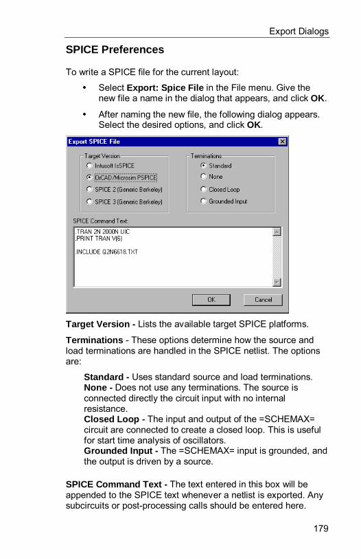
Export Dialogs
179
SPICE Preferences
To write a SPICE file for the current layout:
y Select Export: Spice File in the File menu. Give thenew file a name in the dialog that appears, and click OK.
y After naming the new file, the following dialog appears.Select the desired options, and click OK.
Target Version - Lists the available target SPICE platforms.
Terminations - These options determine how the source andload terminations are handled in the SPICE netlist. The optionsare:
Standard - Uses standard source and load terminations.None - Does not use any terminations. The source isconnected directly the circuit input with no internalresistance.Closed Loop - The input and output of the =SCHEMAX=circuit are connected to create a closed loop. This is usefulfor start time analysis of oscillators.Grounded Input - The =SCHEMAX= input is grounded, andthe output is driven by a source.
SPICE Command Text - The text entered in this box will beappended to the SPICE text whenever a netlist is exported. Anysubcircuits or post-processing calls should be entered here.
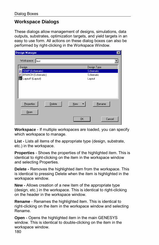
Dialog Boxes
180
Workspace Dialogs
These dialogs allow management of designs, simulations, dataoutputs, substrates, optimization targets, and yield targets in aneasy to use form. All actions on these dialog boxes can also beperformed by right-clicking in the Workspace Window.
Workspace - If multiple workspaces are loaded, you can specifywhich workspace to manage.
List - Lists all items of the appropriate type (design, substrate,etc.) in the workspace.
Properties - Shows the properties of the highlighted item. This isidentical to right-clicking on the item in the workspace windowand selecting Properties.
Delete - Removes the highlighted item from the workspace. Thisis identical to pressing Delete when the item is highlighted in theworkspace window.
New - Allows creation of a new item of the appropriate type(design, etc.) in the workspace. This is identical to right-clickingon the header in the workspace window.
Rename - Renames the highlighted item. This is identical toright-clicking on the item in the workspace window and selectingRename.
Open - Opens the highlighted item in the main GENESYSwindow. This is identical to double-clicking on the item in theworkspace window.
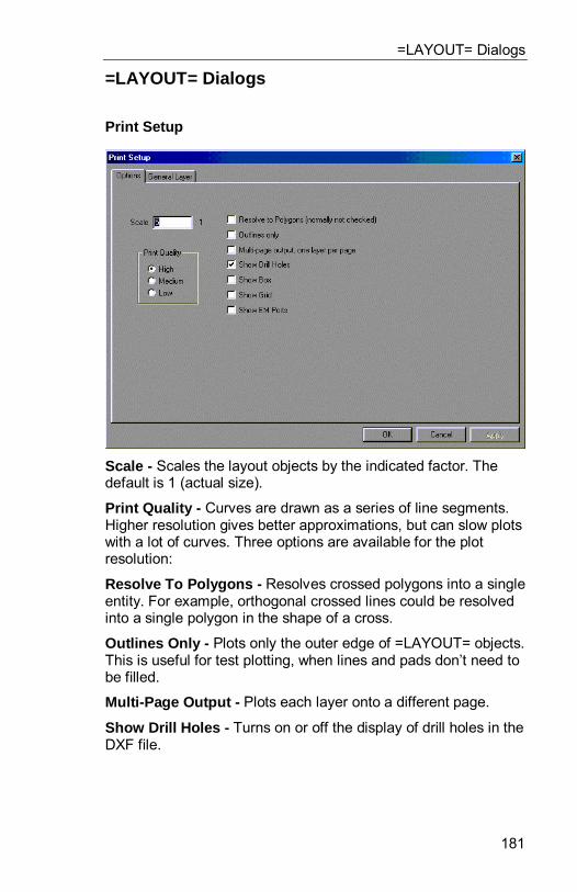
=LAYOUT= Dialogs
181
=LAYOUT= Dialogs
Print Setup
Scale - Scales the layout objects by the indicated factor. Thedefault is 1 (actual size).
Print Quality - Curves are drawn as a series of line segments.Higher resolution gives better approximations, but can slow plotswith a lot of curves. Three options are available for the plotresolution:
Resolve To Polygons - Resolves crossed polygons into a singleentity. For example, orthogonal crossed lines could be resolvedinto a single polygon in the shape of a cross.
Outlines Only - Plots only the outer edge of =LAYOUT= objects.This is useful for test plotting, when lines and pads don’t need tobe filled.
Multi-Page Output - Plots each layer onto a different page.
Show Drill Holes - Turns on or off the display of drill holes in theDXF file.
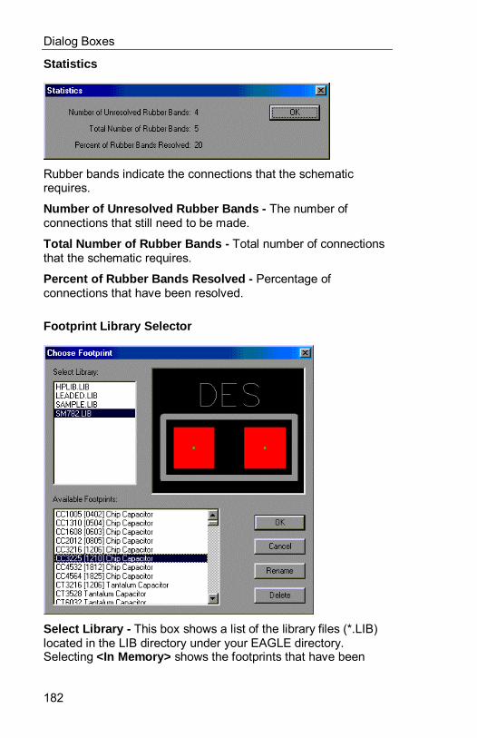
Dialog Boxes
182
Statistics
Rubber bands indicate the connections that the schematicrequires.
Number of Unresolved Rubber Bands - The number ofconnections that still need to be made.
Total Number of Rubber Bands - Total number of connectionsthat the schematic requires.
Percent of Rubber Bands Resolved - Percentage ofconnections that have been resolved.
Footprint Library Selector
Select Library - This box shows a list of the library files (*.LIB)located in the LIB directory under your EAGLE directory.Selecting <In Memory> shows the footprints that have been

=LAYOUT= Dialogs
183
selected and are still in memory. Whenever a new footprint isloaded, it is kept in memory until the program is exited.
Available Footprints - This box shows a list of the footprintsstored in the selected library file.
Preview Window - Shows the footprint selected in the AvailableFootprints box.

Dialog Boxes
184
=LAYOUT= Objects
Overview
The objects available in =LAYOUT= are:
ArcComponentGroupLinePadPolygonPortPourTextViahole
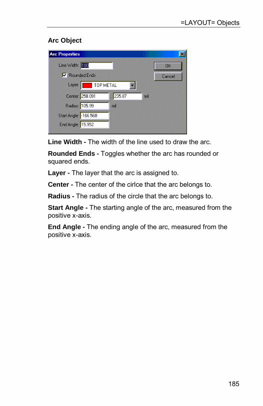
=LAYOUT= Objects
185
Arc Object
Line Width - The width of the line used to draw the arc.
Rounded Ends - Toggles whether the arc has rounded orsquared ends.
Layer - The layer that the arc is assigned to.
Center - The center of the cirlce that the arc belongs to.
Radius - The radius of the circle that the arc belongs to.
Start Angle - The starting angle of the arc, measured from thepositive x-axis.
End Angle - The ending angle of the arc, measured from thepositive x-axis.
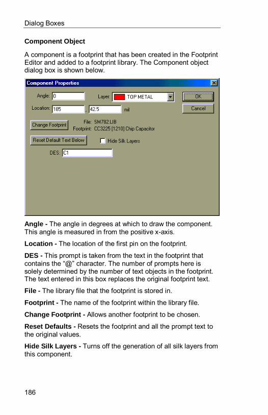
Dialog Boxes
186
Component Object
A component is a footprint that has been created in the FootprintEditor and added to a footprint library. The Component objectdialog box is shown below.
Angle - The angle in degrees at which to draw the component.This angle is measured in from the positive x-axis.
Location - The location of the first pin on the footprint.
DES - This prompt is taken from the text in the footprint thatcontains the “@” character. The number of prompts here issolely determined by the number of text objects in the footprint.The text entered in this box replaces the original footprint text.
File - The library file that the footprint is stored in.
Footprint - The name of the footprint within the library file.
Change Footprint - Allows another footprint to be chosen.
Reset Defaults - Resets the footprint and all the prompt text tothe original values.
Hide Silk Layers - Turns off the generation of all silk layers fromthis component.
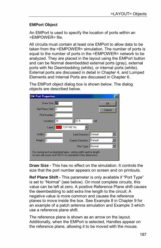
=LAYOUT= Objects
187
EMPort Object
An EMPort is used to specify the location of ports within an=EMPOWER= file.
All circuits must contain at least one EMPort to allow data to betaken from the =EMPOWER= simulation. The number of ports isequal to the number of ports in the =EMPOWER= network to beanalyzed. They are placed in the layout using the EMPort buttonand can be Normal deembedded external ports (gray), externalports with No Deembedding (white), or internal ports (white).External ports are discussed in detail in Chapter 4, and LumpedElements and Internal Ports are discussed in Chapter 6.
The EMPort object dialog box is shown below. The dialogobjects are described below.
Draw Size - This has no effect on the simulation. It controls thesize that the port number appears on screen and on printouts.
Ref Plane Shift - This parameter is only available if “Port Type”is set to “Normal” (see below). On most complete circuits, thisvalue can be left at zero. A positive Reference Plane shift causesthe deembedding to add extra line length to the circuit; Anegative value is more common and causes the referenceplanes to move inside the box. See Example 8 in Chapter 9 foran example of a patch antenna simulation and Example 3 whichuse a reference plane shift.
The reference plane is shown as an arrow on the layout.Additionally, when the EMPort is selected, Handles appear onthe reference plane, allowing it to be moved with the mouse.
Dialog Boxes
188
Port Number - When =EMPOWER= is run, the port numbersspecified here correspond to the port numbers in the resultingdata. These port numbers must be sequential (numbers cannotbe skipped), and Normal ports must always have lower numbersthan non-deembedded and internal ports. =LAYOUT= assigns anew port number automatically when an EMPort is placed, andthe port number is displayed on the layout at the port.
Width & Length - When placing an external port on the end of astrip-type transmission line, you should normally leave these atzero so that =LAYOUT= sizes the port automatically. If you wantto override the size, or for slot-type or internal ports, you canspecify width and length here. Note: Width and length aremeasured relative to the line direction, so these parameters canappear to be reversed. Length is the length in the direction ofpropagation (along the line), and width is the width of the strip.
Layer - Specifies the metal layer on which the port is placed.
Location - Specifies the edge of the port for external ports andthe center of the port for internal ports.
Line Direction - Gives the direction of the line at the port. In thedefault mode, the nearest wall determines the direction of theline. This value rarely needs to be overridden.
Current Dir - Specifies the direction of current flow within theport. Figure 4-3 shows the default current direction for externalports on strip-type structures such as microstrip and stripline.Figure 4-4 shows the default current direction for external portson slot-type structures such as coplanar waveguide. For internalports, the default current direction is “Along Z.” This value alsorarely needs to overridden.
Port Type - Specifies the basic type of port:
Normal ports are external ports which are deembeddedand may be multi-mode. They are shown in gray on thelayout.No Deembed ports are external ports which are notdeembedded and cannot be multi-mode. They are shown inwhite on the layout.Internal ports are also not deembedded and cannot bemulti-mode. They are shown in white on the layout.

=LAYOUT= Objects
189
Group Object
When several objects are selected and the group button isselected on the toolbar (or G is pressed), the objects aregrouped. Whenever any element of the group is selected, theentire group is selected. To break apart the elements once theyhave been grouped:
1. Select the group by clicking on any of the groupelements.
2. Click the ungroup button on the main toolbar or press U.
The Group object dialog box is shown below.
Element List - Shows the elements included in the group object.
Edit Button - Opens the dialog box for the element selected inthe above list.
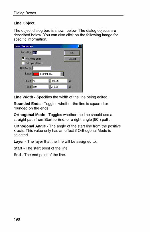
Dialog Boxes
190
Line Object
The object dialog box is shown below. The dialog objects aredescribed below. You can also click on the following image forspecific information.
Line Width - Specifies the width of the line being edited.
Rounded Ends - Toggles whether the line is squared orrounded on the ends.
Orthogonal Mode - Toggles whether the line should use astraight path from Start to End, or a right angle (90 ) path.
Orthogonal Angle - The angle of the start line from the positivex-axis. This value only has an effect if Orthogonal Mode isselected.
Layer - The layer that the line will be assigned to.
Start - The start point of the line.
End - The end point of the line.
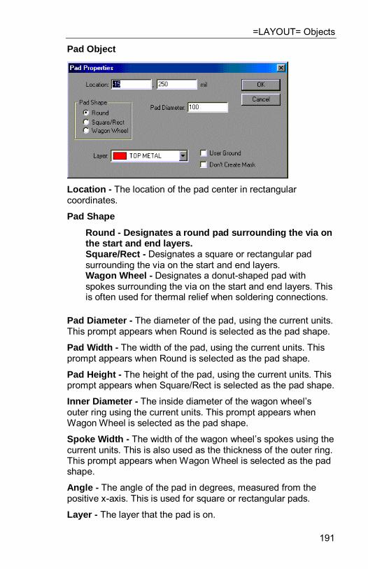
=LAYOUT= Objects
191
Pad Object
Location - The location of the pad center in rectangularcoordinates.
Pad Shape
Round - Designates a round pad surrounding the via onthe start and end layers.Square/Rect - Designates a square or rectangular padsurrounding the via on the start and end layers.Wagon Wheel - Designates a donut-shaped pad withspokes surrounding the via on the start and end layers. Thisis often used for thermal relief when soldering connections.
Pad Diameter - The diameter of the pad, using the current units.This prompt appears when Round is selected as the pad shape.
Pad Width - The width of the pad, using the current units. Thisprompt appears when Round is selected as the pad shape.
Pad Height - The height of the pad, using the current units. Thisprompt appears when Square/Rect is selected as the pad shape.
Inner Diameter - The inside diameter of the wagon wheel’souter ring using the current units. This prompt appears whenWagon Wheel is selected as the pad shape.
Spoke Width - The width of the wagon wheel’s spokes using thecurrent units. This is also used as the thickness of the outer ring.This prompt appears when Wagon Wheel is selected as the padshape.
Angle - The angle of the pad in degrees, measured from thepositive x-axis. This is used for square or rectangular pads.
Layer - The layer that the pad is on.

Dialog Boxes
192
User Ground - Toggles whether the pads are connected toground. Whenever a ground-plane pour is made on the samelayer as these pads, the pour will not keep away.
Don’t Create Mask - Toggles whether to create a solder maskfor the pads associated with this via.

=LAYOUT= Objects
193
Polygon Object
The object dialog box is shown below. The dialog objects aredescribed below. You can also click on the following image forspecific information.
Layer - The layer that the polygon is on.
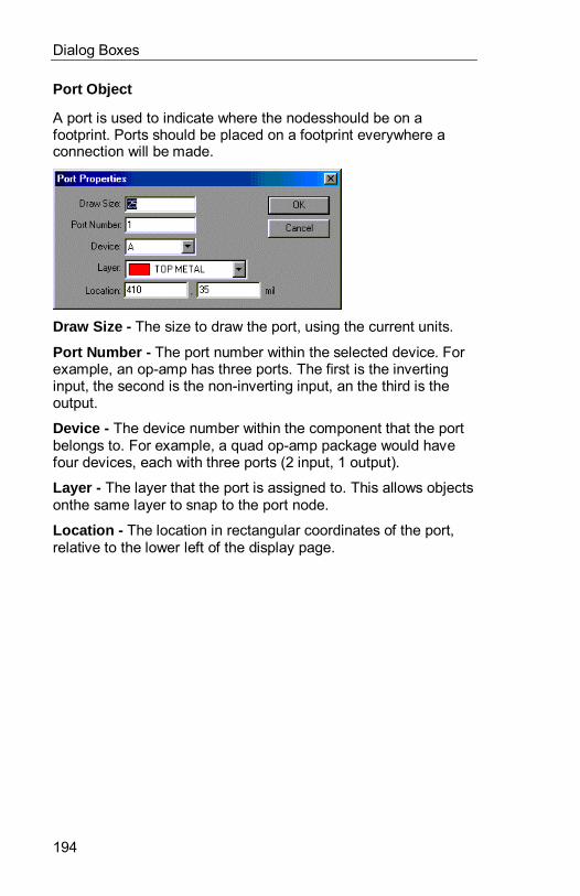
Dialog Boxes
194
Port Object
A port is used to indicate where the nodesshould be on afootprint. Ports should be placed on a footprint everywhere aconnection will be made.
Draw Size - The size to draw the port, using the current units.
Port Number - The port number within the selected device. Forexample, an op-amp has three ports. The first is the invertinginput, the second is the non-inverting input, an the third is theoutput.
Device - The device number within the component that the portbelongs to. For example, a quad op-amp package would havefour devices, each with three ports (2 input, 1 output).
Layer - The layer that the port is assigned to. This allows objectsonthe same layer to snap to the port node.
Location - The location in rectangular coordinates of the port,relative to the lower left of the display page.
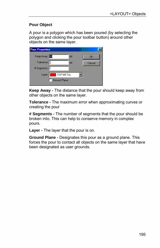
=LAYOUT= Objects
195
Pour Object
A pour is a polygon which has been poured (by selecting thepolygon and clicking the pour toolbar button) around otherobjects on the same layer.
Keep Away - The distance that the pour should keep away fromother objects on the same layer.
Tolerance - The maximum error when approximating curves orcreating the pour
# Segments - The number of segments that the pour should bebroken into. This can help to conserve memory in complexpours.
Layer - The layer that the pour is on.
Ground Plane - Designates this pour as a ground plane. Thisforces the pour to contact all objects on the same layer that havebeen designated as user grounds.
Dialog Boxes
196
Rectangle Object
Start - The lower-left corner of the rectangle.
End - The upper-right corner of the rectangle.
Layer - The layer that the line will be on.
Angle - The rotation angle of the rectangle from the positive x-axis in degrees (counter-clockwise is positive). The rectangle isrotated about the geometric center. The start and endcoordinates are before the rotation.
=LAYOUT= Objects
197
Text Object
Text - The text to be displayed.
Angle - The angle to show the text, measured in degrees fromthe positive x-axis.
Layer - The layer that the text belongs to.
Location - The location of the text, in rectangular coordinates.
Font - The font to use for this text.
Size - The size of this text. This box is only available if UseDefault Size is not selected.
Use Default Size - Toggles whether to use the default size forthis text. See Layout Properties for setting the default text size.
X Justification, Y Justification - Controls the text alignmentwith respect to the specified location. This is most useful forkeeping text centered or aligned when creating a footprint whichwill have different text when the footprint is used.
Dialog Boxes
198
Viahole Object
Drill Di ameter - The diameter of the drill hole.
Location - The location of the drill hole in rectangularcoordinates.
Pad Shape
Round - Designates a round pad surrounding the via on thestart and end layers.Square/Rect - Designates a square or rectangular padsurrounding the via on the start and end layers.Wagon Wheel - Designates a donut-shaped pad withspokes surrounding the via on the start and end layers. Thisis often used for thermal relief when soldering connections.
Pad Diameter - The diameter of the pad, using the current units.This prompt appears when Round is selected as the pad shape.
Pad Height - The height of the pad, using the current units. Thisprompt appears when Square/Rect is selected as the pad shape.
Angle - The angle of the pad in degrees, measured from thepositive x-axis. This is used for square or rectangular pads.
Use Default Layers - Allows the start and end layers for theviahole to be modified when checked. When not checked, thedefaults specified in the Layout Properties dialog are used.
Start Layer - This determines the start layer for the drill hole.This is only available if Use Default Layers is not checked.
End Layer - This determines the end layer for the drill hole. Thisis only available if Use Default Layers is not checked.

=LAYOUT= Objects
199
User Ground - Toggles whether the pads are connected toground. Whenever a ground-plane pour is made on the samelayer as these pads, the pour will not avoid contact.
Don’t Create Mask - Toggles whether to create a solder maskfor the pads associated with this via.
Dialog Boxes
200
=LAYOUT= Properties
General
Designs to Include - This grid shows all available designs toplace on the layout. If a box is checked, the layout will containfootprints and rubber band lines corresponding to the parts inthat design. These footprints and rubber-bands will automaticallyupdate as needed.
Units - The available units for dimensioning objects on thelayout. If you enter a number for a custom unit, simply use aconstant multiplier for converting the unit to millimeters. Somecommon numbers are:
mm 1
mils .0254
meters 1000
inches 25.4
Object Dimensions - Default sizes for most commonly usedobjects. These numbers define the default dimensions line andpad widths, and the drill diameter for viaholes.
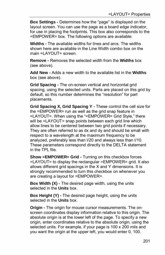
=LAYOUT= Properties
201
Box Settings - Determines how the “page” is displayed on thelayout screen. You can use the page as a board edge indicator,for use in placing the footprints. This box also corresponds to the=EMPOWER= box. The following options are available:
Widths - The available widths for lines and arcs. The widthsshown here are available in the Line Width combo box on themain =LAYOUT= screen.
Remove - Removes the selected width from the Widths box(see above).
Add New - Adds a new width to the available list in the Widthsbox (see above).
Grid Spacing - The on-screen vertical and horizontal gridspacing, using the selected units. Parts are placed on this grid bydefault, so this number determines the “resolution” for partplacements.
Grid Spacing X, Grid Spacing Y - These control the cell size forthe =EMPOWER= run as well as the grid snap feature in=LAYOUT=. When using the “=EMPOWER= Grid Style,” therewill be =LAYOUT= snap points between each grid line whichallow lines to be centered between two grid points if necessary.They are often referred to as dx and dy and should be small withrespect to a wavelength at the maximum frequency to beanalyzed, preferably less than l/20 and always less than l/10.These parameters correspond directly to the DELTA statementin the TPL file.
Show =EMPOWER= Grid - Turning on this checkbox forces=LAYOUT= to display the rectangular =EMPOWER= grid. It alsoallows different grid spacings in the X and Y dimensions. It isstrongly recommended to turn this checkbox on whenever youare creating a layout for =EMPOWER=.
Box Width (X) - The desired page width, using the unitsselected in the Units box.
Box Height (Y) - The desired page height, using the unitsselected in the Units box.
Origin - The origin for mouse cursor measurements. The on-screen coordinates display information relative to this origin. Theabsolute origin is at the lower left of the page. To specify a neworigin, enter coordinates relative to the absolute origin, using theselected units. For example, if your page is 100 x 200 mils andyou want the origin at the upper left, you would enter 0, 100.
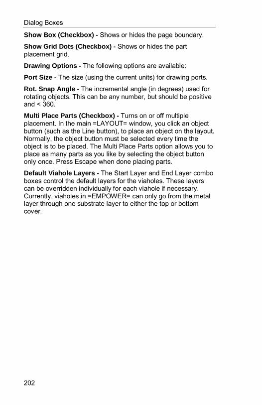
Dialog Boxes
202
Show Box (Checkbox) - Shows or hides the page boundary.
Show Grid Dots (Checkbox) - Shows or hides the partplacement grid.
Drawing Options - The following options are available:
Port Size - The size (using the current units) for drawing ports.
Rot. Snap Angle - The incremental angle (in degrees) used forrotating objects. This can be any number, but should be positiveand < 360.
Multi Place Parts (Checkbox) - Turns on or off multipleplacement. In the main =LAYOUT= window, you click an objectbutton (such as the Line button), to place an object on the layout.Normally, the object button must be selected every time theobject is to be placed. The Multi Place Parts option allows you toplace as many parts as you like by selecting the object buttononly once. Press Escape when done placing parts.
Default Viahole Layers - The Start Layer and End Layer comboboxes control the default layers for the viaholes. These layerscan be overridden individually for each viahole if necessary.Currently, viaholes in =EMPOWER= can only go from the metallayer through one substrate layer to either the top or bottomcover.
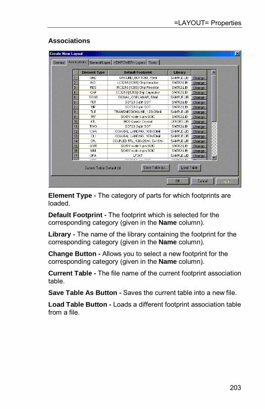
=LAYOUT= Properties
203
Associations
Element Type - The category of parts for which footprints areloaded.
Default Footprint - The footprint which is selected for thecorresponding category (given in the Name column).
Library - The name of the library containing the footprint for thecorresponding category (given in the Name column).
Change Button - Allows you to select a new footprint for thecorresponding category (given in the Name column).
Current Table - The file name of the current footprint associationtable.
Save Table As Button - Saves the current table into a new file.
Load Table Button - Loads a different footprint association tablefrom a file.
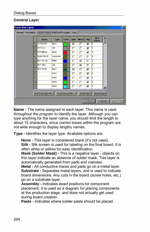
Dialog Boxes
204
General Layer
Name - The name assigned to each layer. This name is usedthroughout the program to identify the layer. Although you cantype anything for the layer name, you should limit the length toabout 12 characters, since combo boxes within the program arenot wide enough to display lengthy names.
Type - Identifies the layer type. Available options are:
None - This layer is considered blank (it’s not used).Silk - Silk screen is used for labeling on the final board. It isoften white or yellow for easy identification.Mask (Solder Mask) - This is a negative layer - objects onthis layer indicate an absence of solder mask. This layer isautomatically generated from pads and viaholes.Metal - All conductive traces and pads go on a metal layer.Substrate - Separates metal layers, and is used to indicateboard dimensions. Any cuts in the board (screw holes, etc.)go on a substrate layer.Assembly - Indicates exact positions for componentplacement. It is used as a diagram for placing componentsat the production stage, and does not actually get usedduring board creation.Paste - Indicates where solder paste should be placed.

=LAYOUT= Properties
205
Color - Shows the selected color for each layer. Click the buttonfor any layer to select another color.
Hide - When selected, the corresponding layer is not shown inthe layout.
Mirror - When selected, the corresponding layer is mirrored(shown reversed) in the layout. This is useful for bottom layers,which would be reversed when viewing the top layer.
Plot - Selects whether to plot the corresponding layer.
Etch Factor - Adds an etch factor to the corresponding layer,using the units selected on the General tab.
Load From Layer File - Loads a new layer configuration from afile.
Save To Layer File - Saves the current layer configuration to anew file.
Insert Layer - Inserts a new layer at the current cursor position.
Delete Layer - Deletes the layer at the current cursor position.
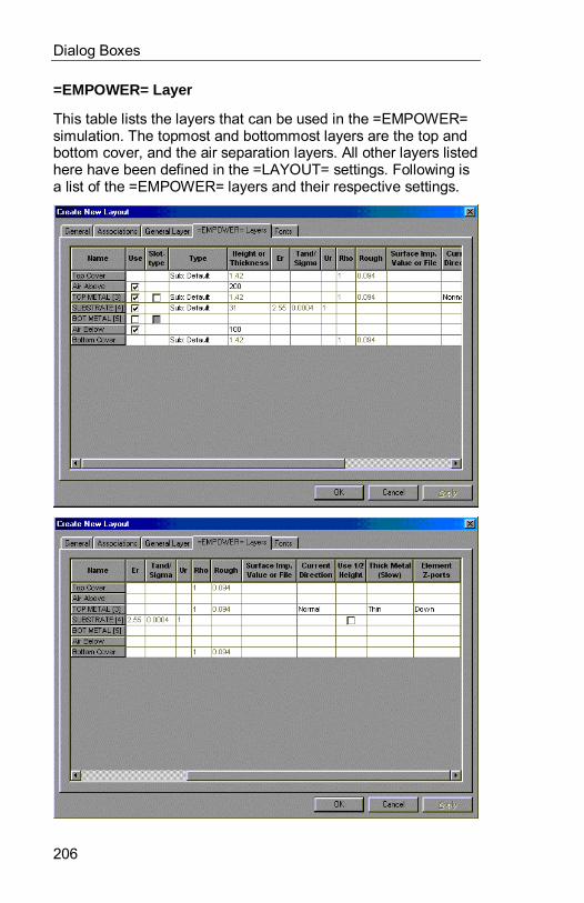
Dialog Boxes
206
=EMPOWER= Layer
This table lists the layers that can be used in the =EMPOWER=simulation. The topmost and bottommost layers are the top andbottom cover, and the air separation layers. All other layers listedhere have been defined in the =LAYOUT= settings. Following isa list of the =EMPOWER= layers and their respective settings.

=LAYOUT= Properties
207
Use - If this box is cleared, the corresponding layer will not beincluded in the =EMPOWER= simulation.
Other entries in this table are different for each type of layer. Tofind help on each column, see the section below for the type oflayer: Top/Bottom Cover, Air Above/Below, Metal, or Substratelayers.
Top Cover & Bottom Cover - Describes the top and bottomcovers (ground planes) of the circuit. Types include:
y Lossless: The cover is ideal metal.
y Physical: The cover is lossy. These losses are describedby Rho (resistivity relative to copper), Thickness, andSurface Roughness.
y Electrical: The cover is lossy and is described by animpedance or file. See the description below under metalfor more information.
y Semi-Infinite Waveguide: There is no cover, and theproblem is simulated as if the box walls and uppermostsubstrate/air layer extend up or down forever (an infinitetube).
y Magnetic Wall: The cover is an ideal magnetic wall. Thissetting is only used in advanced applications.
y Substrates: Choosing a substrate causes the cover toget the rho, thickness, and roughness parameters fromthat substrate definition. We recommend using thissetting whenever possible so that parameters do notneed to be duplicated between substrates and layouts.
Air Above & Air Below - The presence of air at the top of thebox (as in microstrip) or the bottom of the box (as in suspendedmicrostrip) is so common that special entries have been providedfor these cases. Checking the box to turn these layers on is theequivalent of adding a substrate layer with Er=1, Ur=1, andHeight (in units specified in the Dimensions tab) as specified.
Caution: When setting up a new circuit, besure to check the height of the air above, asit is often the only parameter on this tabwhich must be changed, and is thereforeeasily forgotten.
Metal Layers - All metal layers from the General Layer Tab arealso shown in the =EMPOWER= Layer tab. These layers are
Dialog Boxes
208
used for metal and other conductive material such as resistivefilm. The following types are available:
1. Lossless: The layer is ideal metal.
2. Physical Desc: The layer is lossy. These losses aredescribed by Rho (resistivity relative to copper),Thickness, and Surface Roughness.
3. Electrical Desc: The layer is lossy and is described by animpedance or file. This type is commonly used forresistive films and superconductors. If the entry in thisbox is a number, it specifies the impedance of thematerial in ohms per square. If the entry in this box is afilename, it specifies the name of a one-port data filewhich contains impedance data versus frequency. Thisdata file will be interpolated/extrapolated as necessary.See the Device Data chapter for a description of one-port data files.
4. Substrates: Choosing a substrate causes the layer to getthe rho, thickness, and roughness parameters from thatsubstrate definition. We recommend using this settingwhenever possible so that parameters do not need to beduplicated between substrates and layouts.
CAUTION: Unless thick metal is selected,thickness is only used for calculation oflosses. It is not otherwise used, and all stripsare calculated as if they are infinitely thin.
Metal layers have three additional settings available:
Slot Type - Check this box to simulate the non-lossless-metal areas (as opposed to the metal areas) in=EMPOWER=. Use this for ground-planes and other layerswhich are primarily metal. Do not use this for lossy layers.See your =EMPOWER= manual for details.Current Direction - Specifies which direction the currentflows in this layer. The default is along X and Y. "X Only"and "Y Only" can be used to save times on long stretches ofuniform lines. "Z Up", "Z Down", "XYZ Up", and "XYZ Down"allow the creation of thick metal going up/down to the nextlevel or cover.Thick Metal - Checking this box forces =EMPOWER= tomodel the metal including thickness. =EMPOWER= doesthis by putting two metal layers close together, duplicatingthe traces on each, and connecting them with z-directed
=LAYOUT= Properties
209
currents. If thick metal is used, then Current Direction isignored.Element Z-Ports - This setting specifies the defaultdirection for automatically created element ports, either tothe level above or to the level below. Generally, you shouldchoose the electrically shortest path for this direction.
Substrate Layers - All substrate layers from the General LayerTab are also shown in the =EMPOWER= Layer tab. Theselayers are used for substrate and other continuous materialssuch as absorbers inside the top cover. An unlimited number ofsubstrate/media layers can be used. The following types areavailable:
2. Physical w/Tand: The layer is lossy. These losses aredescribed by Height (in units specified in the Dimensionstab), Er (relative dielectric constant), Ur (relativepermittivity constant, normally 1), and Tand (LossTangent).
3. Physical w/Sigma: The layer is lossy. These losses aredescribed by Height (in units specified in the Dimensionstab), Er (relative dielectric constant), Ur (relativepermittivity constant, normally 1), and Sigma (BulkConductivity).
4. Substrates: Choosing a Substrate causes the cover toget the height, Er, Ur, and Tand parameters from thatsubstrate definition. We recommend using this settingwhenever possible so that parameters do not need to beduplicated between schematics and layouts.
CAUTION: For true stripline (triplate), be sureto check the “Use 1/2 Height” checkbox ifyou are using a substrate from =SCHEMAX=.This forces =EMPOWER= to use 1/2 of the=SCHEMAX= substrate height for eachsubstrate (above and below) so that the totalheight for both media layers is correct.
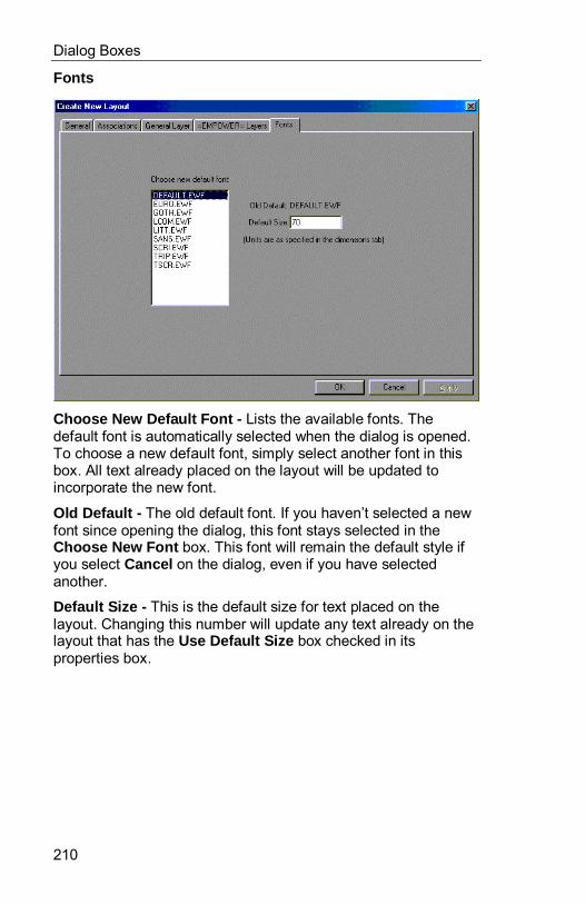
Dialog Boxes
210
Fonts
Choose New Default Font - Lists the available fonts. Thedefault font is automatically selected when the dialog is opened.To choose a new default font, simply select another font in thisbox. All text already placed on the layout will be updated toincorporate the new font.
Old Default - The old default font. If you haven’t selected a newfont since opening the dialog, this font stays selected in theChoose New Font box. This font will remain the default style ifyou select Cancel on the dialog, even if you have selectedanother.
Default Size - This is the default size for text placed on thelayout. Changing this number will update any text already on thelayout that has the Use Default Size box checked in itsproperties box.
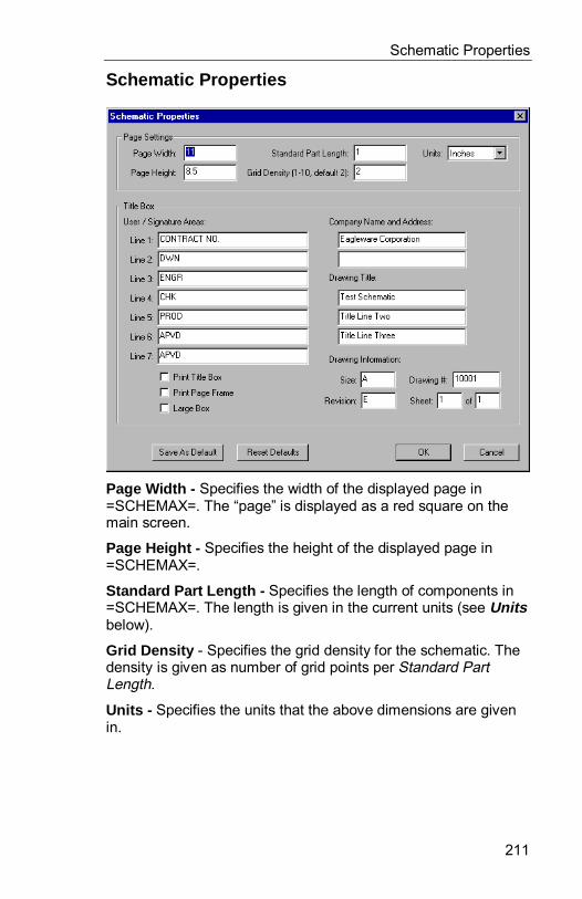
Schematic Properties
211
Schematic Properties
Page Width - Specifies the width of the displayed page in=SCHEMAX=. The “page” is displayed as a red square on themain screen.
Page Height - Specifies the height of the displayed page in=SCHEMAX=.
Standard Part Length - Specifies the length of components in=SCHEMAX=. The length is given in the current units (see Unitsbelow).
Grid Density - Specifies the grid density for the schematic. Thedensity is given as number of grid points per Standard PartLength.
Units - Specifies the units that the above dimensions are givenin.
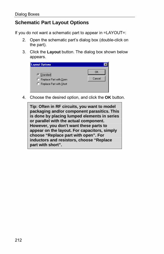
Dialog Boxes
212
Schematic Part Layout Options
If you do not want a schematic part to appear in =LAYOUT=:
2. Open the schematic part’s dialog box (double-click onthe part).
3. Click the Layout button. The dialog box shown belowappears.
4. Choose the desired option, and click the OK button.
Tip: Often in RF circuits, you want to modelpackaging and/or component parasitics. Thisis done by placing lumped elements in seriesor parallel with the actual component.However, you don’t want these parts toappear on the layout. For capacitors, simplychoose “Repl ace part with open”. Forinductors and resistors, choose “Replacepart with short”.
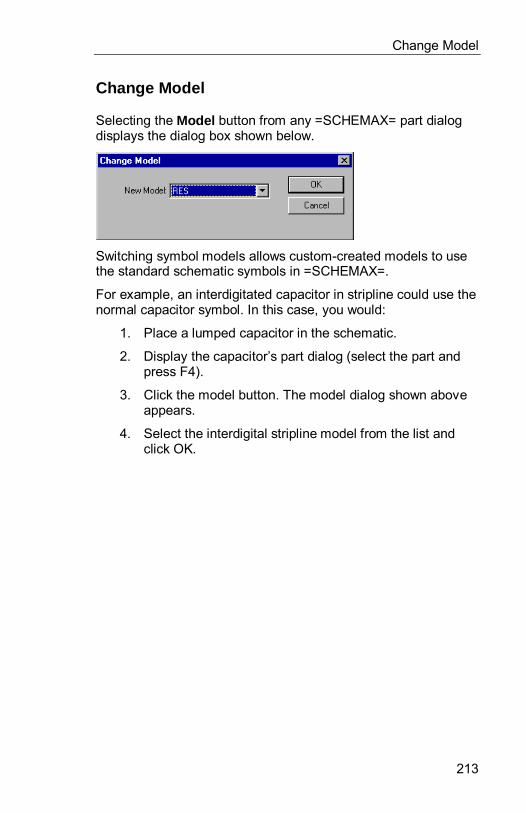
Change Model
213
Change Model
Selecting the Model button from any =SCHEMAX= part dialogdisplays the dialog box shown below.
Switching symbol models allows custom-created models to usethe standard schematic symbols in =SCHEMAX=.
For example, an interdigitated capacitor in stripline could use thenormal capacitor symbol. In this case, you would:
1. Place a lumped capacitor in the schematic.
2. Display the capacitor’s part dialog (select the part andpress F4).
3. Click the model button. The model dialog shown aboveappears.
4. Select the interdigital stripline model from the list andclick OK.
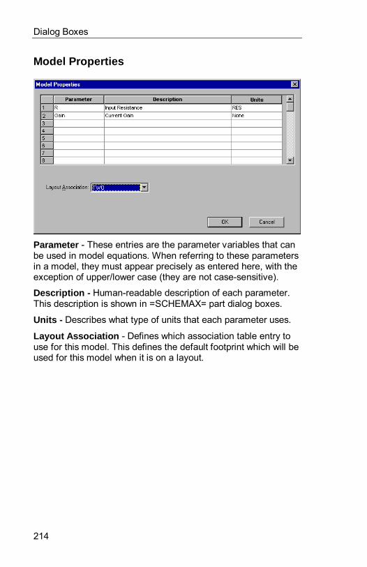
Dialog Boxes
214
Model Properties
Parameter - These entries are the parameter variables that canbe used in model equations. When referring to these parametersin a model, they must appear precisely as entered here, with theexception of upper/lower case (they are not case-sensitive).
Description - Human-readable description of each parameter.This description is shown in =SCHEMAX= part dialog boxes.
Units - Describes what type of units that each parameter uses.
Layout Association - Defines which association table entry touse for this model. This defines the default footprint which will beused for this model when it is on a layout.
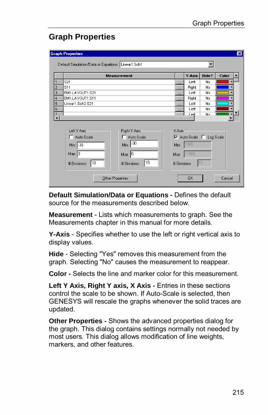
Graph Properties
215
Graph Properties
Default Simulation/Data or Equations - Defines the defaultsource for the measurements described below.
Measurement - Lists which measurements to graph. See theMeasurements chapter in this manual for more details.
Y-Axis - Specifies whether to use the left or right vertical axis todisplay values.
Hide - Selecting "Yes" removes this measurement from thegraph. Selecting "No" causes the measurement to reappear.
Color - Selects the line and marker color for this measurement.
Left Y Axis, Right Y axis, X Axis - Entries in these sectionscontrol the scale to be shown. If Auto-Scale is selected, thenGENESYS will rescale the graphs whenever the solid traces areupdated.
Other Properties - Shows the advanced properties dialog forthe graph. This dialog contains settings normally not needed bymost users. This dialog allows modification of line weights,markers, and other features.
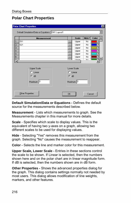
Dialog Boxes
216
Polar Chart Properties
Default Simulation/Data or Equations - Defines the defaultsource for the measurements described below.
Measurement - Lists which measurements to graph. See theMeasurements chapter in this manual for more details.
Scale - Specifies which scale to display values. This is theequivalent of having two y-axes on a graph, allowing twodifferent scales to be used for displaying values.
Hide - Selecting "Yes" removes this measurement from thegraph. Selecting "No" causes the measurement to reappear.
Color - Selects the line and marker color for this measurement.
Upper Scale, Lower Scale - Entries in these sections controlthe scale to be shown. If Linear is selected, then the numbersshown here and on the polar chart are in linear magnitude form.If dB is selected, then the numbers shown are in dB form.
Other Properties - Shows the advanced properties dialog forthe graph. This dialog contains settings normally not needed bymost users. This dialog allows modification of line weights,markers, and other features.
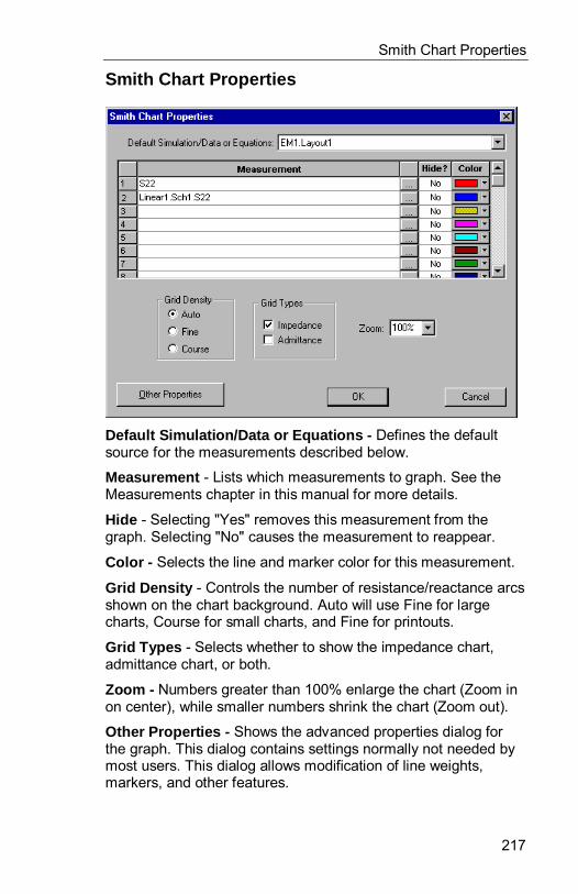
Smith Chart Properties
217
Smith Chart Properties
Default Simulation/Data or Equations - Defines the defaultsource for the measurements described below.
Measurement - Lists which measurements to graph. See theMeasurements chapter in this manual for more details.
Hide - Selecting "Yes" removes this measurement from thegraph. Selecting "No" causes the measurement to reappear.
Color - Selects the line and marker color for this measurement.
Grid Density - Controls the number of resistance/reactance arcsshown on the chart background. Auto will use Fine for largecharts, Course for small charts, and Fine for printouts.
Grid Types - Selects whether to show the impedance chart,admittance chart, or both.
Zoom - Numbers greater than 100% enlarge the chart (Zoom inon center), while smaller numbers shrink the chart (Zoom out).
Other Properties - Shows the advanced properties dialog forthe graph. This dialog contains settings normally not needed bymost users. This dialog allows modification of line weights,markers, and other features.
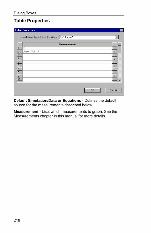
Dialog Boxes
218
Table Properties
Default Simulation/Data or Equations - Defines the defaultsource for the measurements described below.
Measurement - Lists which measurements to graph. See theMeasurements chapter in this manual for more details.
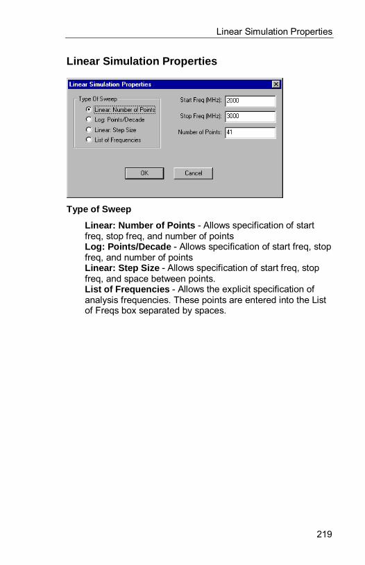
Linear Simulation Properties
219
Linear Simulation Properties
Type of Sweep
Linear: Number of Points - Allows specification of startfreq, stop freq, and number of pointsLog: Points/Decade - Allows specification of start freq, stopfreq, and number of pointsLinear: Step Size - Allows specification of start freq, stopfreq, and space between points.List of Frequencies - Allows the explicit specification ofanalysis frequencies. These points are entered into the Listof Freqs box separated by spaces.
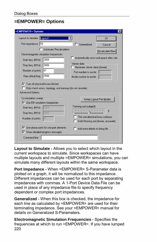
Dialog Boxes
220
=EMPOWER= Options
Layout to Simulate - Allows you to select which layout in thecurrent workspace to simulate. Since workspaces can havemultiple layouts and multiple =EMPOWER= simulations, you cansimulate many different layouts within the same workspace.
Port Impedance - When =EMPOWER= S-Parameter data isplotted on a graph, it will be normalized to this impedance.Different impedances can be used for each port by separatingimpedances with commas. A 1-Port Device Data File can beused in place of any impedance file to specify frequencydependent or complex port impedances.
Generalized - When this box is checked, the impedance foreach line as calculated by =EMPOWER= are used for theirterminating impedance. See your =EMPOWER= manual fordetails on Generalized S-Parameters.
Electromagnetic Simulation Frequencies - Specifies thefrequencies at which to run =EMPOWER=. If you have lumped
=EMPOWER= Options
221
elements in your simulation, you can often turn down the numberof frequencies here and increase the number of frequencies inthe Co-simulation sweep specified below.
Start Freq (MHz) - Specifies the minimum frequency toanalyze.Stop Freq (MHz) - Specifies the maximum frequency toanalyze.Number of Points - Specifies the number of frequencypoints to analyze. Points are distributed linearly between thelow and high freq specified above.Max Critical Freq (MHz) - Specifies the highest importantfrequency that will be analyzed on any run of this circuit.See the “Maximum Critical Frequency” header in Chapter 3(Tips) and the “MAXFRQ” entry in Chapter 11 (TPL FileFormat) of your =EMPOWER= manual for more details.
Automatically save workspace after calc - This checkbox ishandy for overnight runs to help protect against a power outage.Note that checking this box will force the entire workspace to besaved after each run.
Generate Viewer Data (Slower) - Checking this box causes=EMPOWER= to generate a *.EMV file that can be loaded in the=EMPOWER= current/voltage viewer program. Selecting thisbox will increase the amount of time required to solve theproblem. See Chapter 7 of your =EMPOWER= manual for moreinformation on the viewer.
Port number to excite - This option is available if “Generateviewer data” above is checked. It specifies which EMport toexcite for viewer data. By default, mode one is excited, but if theinput is multi-mode, then you can add the option -Imj to excitemode j instead.
Mode number to excite - This option is available if “Generateviewer data” above is checked. It specifies which mode to excitefor viewer data. Generally, mode one is excited, but if the input ismulti-mode, then you can add excite any mode number up to thenumber of modes at that input.
Turn off physical losses (Faster) - If checked, =EMPOWER=will ignore any losses specified in the =EMPOWER= Layer tab.This option is very useful to speed up any preliminary runs.
Only check errors, topology, and memory (do not simulate) -Useful to make sure you have the simulation and layout setupproperly before a long =EMPOWER= run.

Dialog Boxes
222
Co-Simulation Sweep - Specifies the frequencies at which torun simulate the lumped elements + =EMPOWER= datacombination. If you have no lumped elements in your simulation,you should normally check the "Use EM Simulation Frequencies"box. For circuits with lumped elements, you can often save muchtime by using fewer points in the electromagnetic simulationfrequencies above, allowing the co-simulation to interpolate the=EMPOWER= data before the lumped elements are added.
Setup Layout Port Modes - Brings up the multi-mode setupdialog box as described in Chapter 5 (Decomposition) of your=EMPOWER= manual. If this button has exclamation points onit, then multi-mode lines are active.
Thinning out (slider) - Control the amount of thinning. Thedefault thinning out amount is 5. Setting the slider to zero turnsoff thinning. See your =EMPOWER= manual for details onthinning.
Thin out electrical lossy surfaces - If checked, lossy metaldescribed using electrical parameters will also be thinned. Sincethe thinning out model assumes that most current flows on theedges of the lines, this option will be somewhat less accurate forresistive films (where current flows more evenly throughout thematerial). In these cases, you should probably also check theSolid thinning option shown below.
Solid Thinning out (slower) - If checked, slower solid thinningout model is used. This model restores capacitance lost due tothinning out and can be most useful for when large sections ofmetal have been thinned out.
Use planar ports for one-port elements - This box shouldalmost always be checked. When not checked, =EMPOWER=uses z-directed ports at each terminal for all devices. When it ischecked, =EMPOWER= uses in-line ports for elements likeresistors and capacitors (two-terminal, one-port devices). Theonly time this can cause a problem is when you have a linerunning "under" an element (for example, running a line betweenthe two terminals on a resistor, in the same metal layer as theresistor pads).
Add extra details to listing file - If checked, extra informationwhich can be used to double-check your setup is inserted intothe listing file. See Chapter 10 of your =EMPOWER= manual formore details.
Show detailed progress messages - Turning this option offsuppresses almost all output in the =EMPOWER= log. (The

=EMPOWER= Options
223
listing file is not affected.) Turning it off can dramatically speedup very small runs.
Command Line - Any options shown in Chapter 10 of your=EMPOWER= manual which are not covered above can beentered here. One common example is the -On option whichcontrols the size of the box for line analysis.

Dialog Boxes
224
Link to Data File Setup
Filename - Specifies the file containing the Device Data to load.
Browse - Opens a File Open Dialog box so that you can locatethe desired data file.
Number of ports - Specifies the number of ports the data filehas.
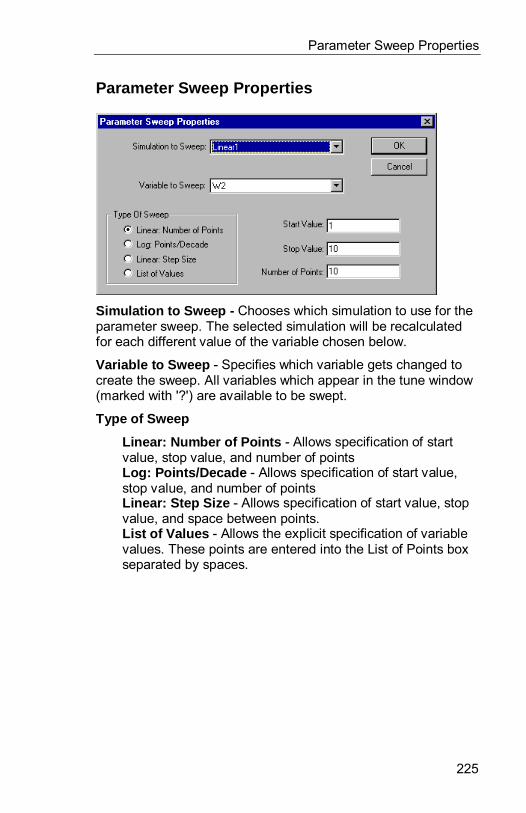
Parameter Sweep Properties
225
Parameter Sweep Properties
Simulation to Sweep - Chooses which simulation to use for theparameter sweep. The selected simulation will be recalculatedfor each different value of the variable chosen below.
Variable to Sweep - Specifies which variable gets changed tocreate the sweep. All variables which appear in the tune window(marked with '?') are available to be swept.
Type of Sweep
Linear: Number of Points - Allows specification of startvalue, stop value, and number of pointsLog: Points/Decade - Allows specification of start value,stop value, and number of pointsLinear: Step Size - Allows specification of start value, stopvalue, and space between points.List of Values - Allows the explicit specification of variablevalues. These points are entered into the List of Points boxseparated by spaces.
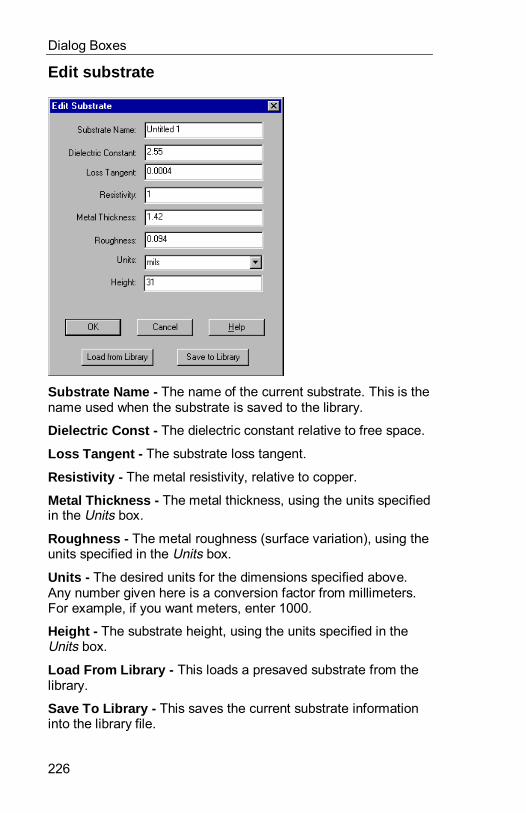
Dialog Boxes
226
Edit substrate
Substrate Name - The name of the current substrate. This is thename used when the substrate is saved to the library.
Dielectric Const - The dielectric constant relative to free space.
Loss Tangent - The substrate loss tangent.
Resistivity - The metal resistivity, relative to copper.
Metal Thickn ess - The metal thickness, using the units specifiedin the Units box.
Roughness - The metal roughness (surface variation), using theunits specified in the Units box.
Units - The desired units for the dimensions specified above.Any number given here is a conversion factor from millimeters.For example, if you want meters, enter 1000.
Height - The substrate height, using the units specified in theUnits box.
Load From Library - This loads a presaved substrate from thelibrary.
Save To Library - This saves the current substrate informationinto the library file.
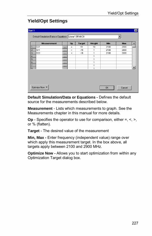
Yield/Opt Settings
227
Yield/Opt Settings
Default Simulation/Data or Equations - Defines the defaultsource for the measurements described below.
Measurement - Lists which measurements to graph. See theMeasurements chapter in this manual for more details.
Op - Specifies the operator to use for comparison, either =, <, >,or % (flatten).
Target - The desired value of the measurement
Min, Max - Enter frequency (independent value) range overwhich apply this measurement target. In the box above, alltargets apply between 2100 and 2900 MHz.
Optimize Now - Allows you to start optimization from within anyOptimization Target dialog box.
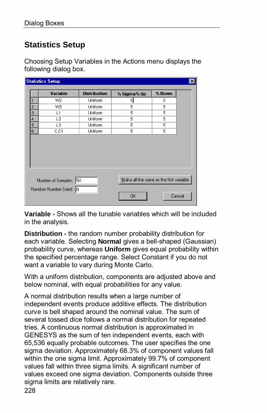
Dialog Boxes
228
Statistics Setup
Choosing Setup Variables in the Actions menu displays thefollowing dialog box.
Variable - Shows all the tunable variables which will be includedin the analysis.
Distribution - the random number probability distribution foreach variable. Selecting Normal gives a bell-shaped (Gaussian)probability curve, whereas Uniform gives equal probability withinthe specified percentage range. Select Constant if you do notwant a variable to vary during Monte Carlo.
With a uniform distribution, components are adjusted above andbelow nominal, with equal probabilities for any value.
A normal distribution results when a large number ofindependent events produce additive effects. The distributioncurve is bell shaped around the nominal value. The sum ofseveral tossed dice follows a normal distribution for repeatedtries. A continuous normal distribution is approximated inGENESYS as the sum of ten independent events, each with65,536 equally probable outcomes. The user specifies the onesigma deviation. Approximately 68.3% of component values fallwithin the one sigma limit. Approximately 99.7% of componentvalues fall within three sigma limits. A significant number ofvalues exceed one sigma deviation. Components outside threesigma limits are relatively rare.
Statistics Setup
229
% Sigma - Specifies one standard deviation (as a percentage ofthe nominal component value). This applies if NormalDistribution is selected.
% Up - Specifies the percentage tolerance above the nominalvalue for the selected variable. This applies if UniformDistribution is selected.
% Down - Specifies the percentage tolerance below the nominalvalue for the selected variable.
Make all the same as the first variable - Sets all variabletolerances and types to the same value.
Number of Samples - Specifies the number of random sampleruns for each Monte Carlo analysis.
Random Number Seed - Specifies a seed for the randomnumber generator. Random numbers used for componentdistribution are derived from the specified seed. Enter an integerseed between -2000000 and +2000000. Runs with the sameseed, circuit file and sample size are identical. This provides theuser with both the ability to repeat a specific run or to create avirtually unlimited number of different runs of a specified samplesize.

Chapter 8: Error MessagesThis chapter has four sections: General, Touchstone Export,SPICE Export, and =EMPOWER= Messages.
General
A fatal internal =SCHEMAX= error has occurredIf this error occurs, please contact Eagleware.
A node number was expected wh ere __ was found, lineThis error occurs on a component line. Check the line numberand change the indicated string to a node number in the editor.
Ambiguous keyword __ on line __You have abbreviated the title of a component value to anambiguous name, such as NA for NARROW or NAME.
__ can only be used with 2-port data at __.Some output parameters, such as circles and noise, are onlyvalid for two port data.
Cannot find S or Y-parameter device data file __. Checkfilename. The name may need a full path such asC:\EAGLE\EXAMPLES\MRF901.615 orC:\SDATA\MOTOROLA\2NXXXX\2N6618A.A03The S- or Y-parameter file specified on a TWO code line was notfound. Check the filename. Check that the file exists in thedefault or specified directory. The filename may need to includea pathname.
Data in file __ does not cover the analysis frequency range.The data has been extrapolated.The data file does not contain data at low or high enoughfrequencies. The extrapolation may not be valid for the givendevice.
Different names found on input and output of networkIf both the input and the output of a network are named, thenames must be exactly the same. Choose one name and deletethe other one.
Error in format (#) line of S-parameter data file.The line beginning with "#" of the specified S-parameter data fileis invalid. Check this line in the S-parameter file.
Error Messages
232
FUNCTIONs nested too deeply (__ levels maximum). Currentfunction is __.Check to see that you have not used a recursive function (afunction that calls itself).
FUNCTION Parameter __ is declared twice at __The FUNCTION declaration has two or more parameters withthe same name.
FUNCTION _ is declared twice (first declaration was at )The same FUNCTION name has been reused.
G and H Parameter files can only be used for loading two-port data in data file __.G and H parameters are undefined for other numbers of ports(eg, 1 or 3).
Incorrect form for IF-THEN statement at __An IF-THEN statement in the EQUATE block had an incorrectformat.
Incorrect function at (__) at __=SuperStar= is expecting a function such as SIN(x) or COS(x).The indicated function is not valid.
Incorrect function call __ at __The syntax is invalid or the function name is unknown.
Incorrect number of parameters sent to FUNC TION __The number of parameters used does not match the number ofparameters in the FUNCTION declaration.
Incorrect number of parameters sent to MODEL __ at __The number of parameters used does not match the number ofparameters in the MODEL definition.
Incorrect number of noise parameters on a line in data file__. Each frequency must include an additional fourparametersThe data file does not contain complete noise data on thespecified line. See Chapter 5 for more information.
Incorrect number of parameters at __.Check to see that the parameters are as expected.
Incorrect number of RX parameters on a line in data file __.Each frequency must include two additional parameters.The data file does not include complete RX data on the specifiedline. See Chapter 5 for more information.
General
233
Incorrect number of S-Parameters in data file __. Eachfrequency must include the correct number of parameterswith spaces between each as the delimiter.Each line in an S- or Y-parameter data file must have ninenumbers. One for the frequency in megahertz and eight for themagnitudes and angles. See Chapter 5 for details.
Invalid DEFnP line for MODEL at __The DEFnP name should match the model name. Also, checkthe number of nodes, it should match the DEFnP .
Invalid EQUATE statement at __There is a syntax error in the EQUATE statement.
Invalid FUNCTION decl aration at __There is a syntax error in the FUNCTION declaration.
Invalid GOTO statement at __There is a syntax error in the GOTO statement.
Invalid LABEL statement at __There is a syntax error in the LABEL statement.
Invalid MODEL declaration at __There is a syntax error in the MODEL declaration.
Invalid number (__) found at __This error occurs in the equation block. =SuperStar= is lookingfor a number that is not present.
Invalid operator (__) at __Only valid operators may be used, such as "+", "-", "*", etc.
Invalid or unknown parameter name (__) at __.Check to see that the parameter name is valid.
Invalid port number used (__) in network __.Port numbers must be a single digit between 1 and 9.
Invalid use of DEFnP at __. Valid Examples: DEF2P 1 5NAME, DEF4P 1 4 3 5 COUPLERThe DEF2P code must contain two nodes and a name for thenetwork. Check the indicated line.
Invalid use of not operator (~) at __The not operator is a unary operator and must precede the valueto operate on.
Label __ has already been defined at __A Label can only be used once.
Error Messages
234
Libraries nested too deeply (__ levels maximum). Currentfilename is __.Check to see that you have not used a file that loads itself.
Maximum node number is 9999 at __.Only use node numbers between 0 (ground) and 9999.
MODEL __ is declared twice (first declaration was at __)The model name specified has already been defined.
MODEL declarations must end with a DEFnP line at __All models must declare the equivalent circuit followed by aDEFnP line.
MODEL declarations must only have one DEFnP line, and notext may follow the DEFnP line at __A possible cause of this is forgetting to put a block label
MODEL Parameter __ is declared twice at __The MODEL declaration has two or more parameters with thesame name.
Models should contain exactly one network. This sch ematiccontains __ networks.Each model definition can only contain one model and may notcontain sub-networks.
Multiple port #__'s found in network __There may be multiple networks on a schematic, but there maybe only one of each port # in a network.
Networks contain circular references. Cannot write file.Your schematic has two or more networks that are referring toeach other. You must redesign the schematic so that circularreferences no longer occur.
No format line (#) found in data file __. We are assuming thisdata file to be in MHz, __ Parameter, __, %lg ohm. Pleaseadd a format line to the data file.All data files must have a format line.
No name given for a NET block. Name all NET blocks withthe name of the referenced network.The NET block contains an invalid network name.
No name given for a network. This name must be specifiedin the input.Each network must have a name on either the input or output,specified through the input or output dialog boxes. After placingthe INP on the circuit, you are automatically asked for a name.
General
235
No samples met yield criteria. Either Restart with slowersetting or use Monte Carlo Setup to either changecomponent tolerances or increase the number of samples.Yield optimization must find at least one sample which meets theyield criteria.
No noise data found in file __. We have assumed the data tobe passive.If you intend to use a device for noise analysis, you shouldensure that the data file contains noise data.
No values are marked for optimization.No values are marked for tuning.Values to tune or optimize must be preceded by a "?".
__ only contains __-port data so __ cannot be displayedFor instance, S32 cannot be displayed for a 2-port.
Operator __[] can only be used with circles.Operator __[] can only be used with complex quantities.Operator __[] can only be used with gain circles.Operator __[] can only be used with noise circles.Operator __[] can only be used with stability circles.The given operator can only be used with the given type. Forexample, RAD can only be used with circles (to find the radius).
Optimization frequencies do not cover any analysis pointsat __. (Requested __ to __, but nearest points are __ and __.)The frequency range requested for optimization is within thesweep range, but the discrete points do not lie on the sweeppoints.
Port #__ connected directly to ground in network __Ports cannot be connected directly to ground.
Port #__ is missing in network __.Each network must use port numbers sequentially. Use the INand OUT buttons to place them on your schematic.
Substrate names beginning with Default cannot be saved tothe library. Rename the substrate and resave it.The subtrate has Default in its name. Default is reserved for thedefault substrate in =SCHEMAX=. Although the default substratecan be chosen, no substrate can be named default.
Too few parameters in part __More parameters must be specified for the indicated part.
Too few parameters on __More parameters must be specified on the indicated line.
Error Messages
236
Too many parameters on __There are too many parameters on the indicated line.
Too many pins for model __ used in part __.The element used in =SCHEMAX= for a model has too manypins (terminals).
Two or more format (#) lines found in data file __.Data files can only contain one format line.
Undefined substrate __ used in part __You must specify the substrate you want to use in the dialog boxfor each part. Use the Substrate menu to add a substrate or editan already existing substrate.
Undefined variable __ or incorrect mathematical functionA variable was used in the CIRCUIT or EQUATE blocks whichhasn't been assigned a value.
Undefined variable __ or incorrect mathematical functionduring MODEL expansion at __An undefined variable was found inside a MODEL declaration.Edit the model to fix the problem.
__: Unknown label in equation blockA label was specified by a GOTO which was not defined.
Unknown variable or invalid number __ at __Check the spelling for a variable, or make sure that the letter O isnot used for a zero (0).
Unmatched parentheses at __Unmatched opening or closing parentheses were found.
Unnamed NET block found in network __. Name all NETblocks with the name of the referenced network.Name all NET blocks with existing network names.
Unrecognized keyword (__) on line __The command indicated is not a =SuperStar= keyword.
Warning: Part connected between grounds has no effect.There is a part that has ground on both ends. Note that a voltagesource is considered an RF ground.
Unknown Operator __[].The specified operator is not correct. See Operator reference.
Measurement "__" does not contain an operator, such asDB[] (e.g., DB[S21]). An operator must be specified for allmeasurements in equation blocks
General
237
For example, Change Linear1.Sch1.S11 toLinear1.Sch1.DB[S11].
There are no global equations in this workspace. SelectEquations from the Workspace menu to create equations.Measurement "__" cannot be used without global equations.You have requested to graph or optimize equation data, butnone was found.
Equate variable "__" does not swept (x vs. y) data. Normalnumbers and matrices cannot be used as measurements.Create a Variable Viewer output to see the values of variables.
Analysis/Data "__" does not contain "__". Measurement"__" cannot be created.Analysis/Data "__" contains multiple members. You mustspecify which data within the analysis to use. Measurement"__" cannot be created.Workspace "__" does not contain Analysis/Data "__".Measurement "__" cannot be created.Workspace "__" not found. Measurement "__" cannot becreated.Workspace/Analysis/Data "__" not found. Measurement "__"cannot be created.Workspace "__" contains multiple Analysis/Data items. Youmust specify analysis/data to use. Measurement "__" cannotbe created.See the measurements chapter in the reference manual fordetails on creating measurements.
Too many periods in measurement "__".See the measurements chapter in the reference manual fordetails on creating measurements.
The default context for equation based measurements mustbe "Equations". Context "__" is invalid.See the measurements chapter in the reference manual fordetails on creating measurements.
This file was saved in a newer version of GENESYS and maynot be compatible with this version.You should not attempt to load files from a newer verion ofGENESYS, such as 7.0, into an older version, such as 6.5.
Error Messages
238
Touchstone Export
Error in Touchstone Validation parameter (TCHVALID).This error should not occur.
Error in Touchstone Parameter Translation (TCHPARM).This error should not occur.
If units other than MM are used, CPL/TLP parts must not usea variable or a tuned value for length.The indicated part has a variable or tuned length, but the currentsubstrate uses units other than 1.
Warning: In Touchstone, attenuation in CPL/CLINP is notfrequency dependent.Touchstone's attenuation is constant with frequency, and mayvary from =SuperStar='s frequency dependent model.
Warning: In Touchstone, attenuation p arameters arerequired in CPL/CLINP. Using 1E-9 for AE and AO.The indicated part is missing attenuation parameters. The valueshown has been substituted during translation.
Warning: In Touchstone, frequency and attenuationparameters are re quired in TLE/TLINP. Using 1E-9 for A and1000 for F in part __.Either frequency or attenuation was left out of the indicated part.The values shown have been substituted.
Incomplete or missing parameter on line __ of text portionof schematic.The line does not have a complete parameter list.
Invalid output types (__).The indicated output selection is not supported.
Missing frequency in FREQ block.The FREQ block is missing a parameter. Check the outputrequest line for missing parameters.
Missing frequency in OPT block.The OPT block is missing a parameter. Check the optimizationrequests for missing parameters.
Missing parameter in part __.The part is missing a required value for translation.
Missing parameter in substrate __ used in part __.The indicated substrate is missing a required parameter fortranslation of the indicated part.
Touchstone Export
239
Warning: MST asymmetrical does not have a Touchstoneequivalent in part __. Using symmetrical.Self explanatory.
Warning: MVH radius cannot be tuneable in part __.A tuneable radius is not allowed for translation.
Warning: Only one unit type per circuit is allowed.Conflicting units were found on different substrate declarations.Units must be consistent throughout the circuit for translation.
Required parameter (_) was not given in part _ of type _.A parameter was not given which is Touchstone requires.
There is no schematic to translate!The schematic is empty
Touchstone does not support __ in part __.The indicated part is not supported for translation.
Touchstone does not support E12 for optimization.E12 has been selected for optimization, but cannot be translated.
Touchstone does not support E12 for output.E12 has been requested, but cannot be translated.
Warning: Touchstone does not support full nodal noiseanalysis.Noise figure data was requested, but is not available forcomplete circuit simulation (Available for devices only).
Touchstone does not support IF, GOTO, and LABEL fromthe =SuperStar= EQUATE block.Conditionals were found in the EQUATE block, but are notsupported for translation.
Warning: Touchstone does not support Polar charts (POL),using Smith charts instead.POL in the WINDOW blocks has been translated to SMH.
Warning: Touchstone does not support the flatten op erator(%).The delay flatten operator is not supported in Touchstone.
Warning: Touchstone does not support Zo.In Touchstone, these elements use the terminating impedance ofthe network as Zo.
Warning: Touchstone does not support thickn ess.Use care: The resulting simulation may not be accurate.
Error Messages
240
Touchstone only supports a transformer secondary of onein part __.The indicated transformer must use a secondary of 1. Divideeach side by the secondary number to adjust, if no variables areused.
Warning: __ - Touchstone only supports one frequencyrange per circuit file.More than one frequency range has been specified, but only thefirst will be used.
Touchstone only supports one set of terminations per 2-portname. Window __ is used more than once with differentterminations.The indicated window has been used before with differentterminations. This is not allowed in Touchstone.
Touchstone only supports the TR (turns ratio) transformeroption in part __.The indicated transformer has impedance ratio selected, butmust use turns ratio for translation.
Warning: Touchstone parts PRC, PRL, PRLC, SRC, SRL, andSRLC do not support Q in part __.The element has been translated using ideal L's and C's.
Touchstone requires nodes 3 and 4 of GYR (gyrator) to begrounded in part __.The indicated nodes must be connected directly to ground.
Touchstone requires the third node of NET parts to begrounded in part __.The third node of the indicated network block must be connecteddirectly to ground.
Touchstone requires the last node to be grounded in THR,FOU, and NPO in part __.The indicated node must be connected directly to ground.
Touchstone substrate model for __ requires a heightThe part requires a height, but none was specified.
Touchstone translations don't support postprocessing.Combined responses are not translatable.
Touchstone uses only specific units. Valid values are:0.001(UM), 0.0254(MIL), 1.0(MM), 10(CM), 25.4(IN), and1000(M). Check the default substrate.One of the substrates contained in the circuit does not use oneof the above units.
Spice Export
241
Touchstone's BIP and FET models are not compatible with=SuperStar=. Use TWO instead.The models used by Touchstone do not coincide with the=SuperStar= transistor models. Use S-Parameter devicesinstead, or edit the translated file and use a Touchstone model.
Warning: Touchstone's TLIN model does not use anattenuation model in part __.The indicated part has an attenuation specified, butTouchstone's model will not include it.
__ - Unknown frequency code.The indicated line contains an error.
Unrecognized DSP option __.The indicated paramter is not supported for display, and cannotbe translated.
Unrecognized GPH option __.The indicated option is not supported for output selection.
Validation error (__) in part __ of type __.The part cannot be translated accurately to Touchstone due tothe condition shown.
Variables cannot be used in place of frequency in FREQblock.A variable, or non-number has been used where a numbershould have been in the FREQ block.
Variables or tunable elements may not be used within theMUI model in part __.The indicated part contains variables or tunable values, andcannot be translated.
Spice Export
Warning: Cannot find subcircuit __ ref erenced by __ incircuit __.An undefined network name was referenced in the indicatedcircuit.
Equations with operators (such as '+' or '-') can't beexported to Spice. The first illegal line is __. Edit the textand replace it with a simple assignment such as X=5.The indicated line contains an illegal equation.
Error writing file __.The indicated file was not written due to a file error.
Error Messages
242
Invalid filename, cannot write Spice file.The filename chosen is not valid, and can't be written to.
Invalid subcircuit reference at nodes __.The indicated nodes are connected to an undefined or unnamedsubcircuit.
Warning: OpAmp subckt X $__ is a only a simplifiedapproximation; Crossover frequency is not modeled.The indicated op-amp does not model frequency-dependentgain.
Primary Circuit (_) not found. Check Spice Preferences.An undefined network name was given for the primary circuittranslation.
Selected SPICE version(__) does not support __ parts.The SPICE target version does not support the part.
SPICE does not support __ parts.SPICE does not support the indicated parts.
Spice does not support ideal TRF's. Part __ should bereplaced by an MUI.The indicated part is not an ideal transformer. Instead, usemutually coupled inductors (MUI).
There is no schematic to translate!Export was selected, but there is no schematic loaded.
User defined device __ at nodes __ is missing userparameters.The indicated device is missing parameters.
=EMPOWER=
All PADs will be no rmalized to ___ Ohms to generate viewerdata.Terminations for internal ports are not defined in =EMPOWER=unless the normalization impedance is entered directly in the -NIoption. The terminations are necessary only to compute data forvisualization. The internal inputs will be terminated by theimpedance specified in this message (1 Ohm) to generate theviewer data files *.EMV and (or) *.PLX.
Bad frequency range (___ to ___) at ___The frequencies F0 and F1 from the EMFRQ line should bepositive, and F0 must be less than or equal to F1.
=EMPOWER=
243
Both physical and electrical parameters specified at ___.Physical parameters will be used.Either physical (RHO, TMET, ROUGH) or electrical (Z)parameters of a surface can be used to describe the physicalproperties of a a top or bottom wall in the package block or asurface in the geometry block, but not both.
Cannot normalize impedance matrix.Normalization failure due to uncertain or zero value of anexternal port normalization impedance. Check the geometry ofthe problem, delete relevant de-embedding data files (*.RGF or*.Ln) and rerun.
Cannot transform immitance matrix to S-matrix.The normalized impedance or admittance matrix of the problemis singular. This happen for some particular circuits and as anaftereffect of a resonance occurring in the structure. A chance ofthe last event is very low, so change slightly frequencies orintroduce physical losses in the structure and if the problempersists check the normalization coefficients and the geometry.
Contact support group. Occurred: ___.An unexplainable problem occurred in the specified programblock. It could be a warning or a fatal error. Check the geometry,delete all output and auxiliary files related to the problem andrerun. If it did not help, send Eagleware the schematic or TPL fileand all relevant input data files.
Dielectric constant of media layer number __ (___) is invalid.Must be > 1, and < __.The relative permittivity of a media layer must be real valuegreater then or equal to 1 and less then the indicated value.
Different order of the inputs regions.A multiconductor or multimode line segment should havemodally connected ports at the opposite sides of the segmentnumbered sequentially starting from one side of the box. It isvalid if the line analysis mode is directly specified (EMLINE),otherwise the structure with wrong numeration will be treated asa discontinuity with different inputs at the opposite sides of thesegment.
Duplicate PORT/PAD node number found at ___.All inputs must be enumerated sequentially and have distinctnumbers.
END_PACKAGE not found.The package block of the TPL file must be terminated by theEND_PACKAGE line.
Error Messages
244
Error: Normal =EMPOWER= ports (shown in gray) musthave lower numbers than nondeembedded ports or pads(white). For example, you should switch the port numberson =EMPOWER= ports __ and __.All inputs must be enumerated sequentially and have distinctnumbers. Also, the inputs to be de-embedded must beenumerated first.
Fatal Error: Can not open file: ___A generic message for all kinds of files. The most common case:the specified TPL file (input data file) does not exist in thespecified directory. This message may also arise if the programcan not open exchange files (*.SS,*.Rn), an admittance matrixfile (*.Y) or a de-embedding data file (*.RGF or *.Ln). A crash ofthe program in a previous run could cause it. Try to fix corruptedfiles before further runs.
Fatal Error: Can not open output file: ___A listing file open error. The listing file might be corrupted forsome reason, or your hard drive might be full
Fatal Error: Can not read from file: ___An error when reading a de-embedding file (*.RGF or *.Ln) or anadmittance matrix file (*.Y). Delete the file and rerun=EMPOWER=.
Fatal Error: Can not set position in file: ___An error when reading or writing a de-embedding file (*.RGF or*.Ln) or an admittance matrix file (*.Y). Delete them and rerun=EMPOWER=.
Fatal Error: Can not write to file: ___An error when writing a de-embedding file (*.RGF or *.Ln) or anadmittance matrix file (*.Y). Delete the specified file and rerun=EMPOWER=. Also, check hard drive space.
Fatal error: Not enough memory.The problem does not fit to the total available RAM of thecomputer. Check out all messages of the memory estimationprogram in the listing file (MEMORY section) and try to figure itout how to reduce the problem (see the Tips Chapter). Ifeverything is as expected you can use the -VM option to let theprogram use the virtual memory more freely, however, addingmore RAM is a better solution. The program only allows the useof virtual memory in a rational way and this message occurs onlyif some computationally intensive parts of the simulation requiresubstantial hard disk space to be completed.

=EMPOWER=
245
Fatal Error: Out of memory during parsing of input file.An error occurred related to allocation of memory duringprocessing of the TPL file.
Fatal Error: Wrong file label: ___The program tried to treat a wrong file as a descriptor file (*.Y) ora de-embedding file (*.RGF or *.Ln). The descriptor file shouldbegin with the label YMT, and the de-embedding file alwaysstarts with the RGF. Check it out, remove the relative files andrerun.
Fatal Error: Wrong file version: ___Can occur when running a new version of =EMPOWER= withsome files prepared using a previous version of the program (orvice versa). It happens only if the format of the file has beenchanged and are not compatible.
Few topology definitions for layer number __.Each signal layer geometry block must have a distinctive numbercorresponding to the signal layer in the package block.(Multilevel signal layer version only, should not occur yet as ofthe printing of this manual.)
File n ame too long.The total length of a file name (including path) must be less then256 characters.
First Polygon point (X1,Y1) must be specified at ___Polygonal region vertexes must be enumerated and enteredsequentially starting from (X1,Y1).
Height of media l ayer number __ (___) is invalid. Must be >__, and < __.An acceptable media layer thickness or height value isconstrained by the values indicated in the message. The actualvalue and limits are given in meters.
Illegal d escription of layer number __.The signal or metal layers (the LAYER keyword) must benumbered starting from 1 and entered sequentially in thepackage block.
Illegal dimension of p ackage along __ axis( ___ ).The shielding box dimensions along X- and Y-axis defined in theSIZE line must be real positive numbers greater then zero.
Illegal keyword (___) in description of ___ wall at ___The top and bottom wall TYPE parameter can assume valuesMETAL, MAGNETIC or OPEN.
Error Messages
246
Illegal number of p arameters at ___The frequency sweep line EMFRQ must have three parameters:F0, F1 and COUNT.
In line mode, only rectangles and ports may be used.A structure can be treated as a line segment if it contains onlyexternal inputs (PORT) and rectangular metallized regions(RECT).
Inappropriate line length (___ mm) for analysis at ___ MHz.Decrease length and try again.The structure in the line analysis mode does not behave as a linesegment due to some irregularities or singularities inside. Thus,the line parameters and de-embedding data could not becalculated. Change the line segment length if you are trying toanalyze a line. If this happens during automatic de-embedding,change the default lengths of the line segments using thecommand line option -On (n>1).
Information: Bottom and top coordinates are reversed onsome elements.Coordinates X1, Y1 in the RECT descriptor should correspond tothe left bottom corner and X2,Y2 should correspond to the righttop corner of a rectangular region.
Information: Left and right coordinates are reversed onsome elements.Coordinates X1, Y1 in the RECT descriptor should correspond tothe left bottom corner and X2,Y2 should correspond to the righttop corner of a rectangular region.
Input __, mode __ will be excited instead of specified input__, mode __.Either the port or mode number specified in the options -In and -Im to excite an incident eigenwave do not correspond to a port ormode of the actual structure. The program will set a defaultincident wave.
Input number __ doesn't touch side wall.The external ports should touch a sidewall. The proximity iscontrolled by the input position parameter TOLERANCE.
Input number __ has regions with different lengths.All surface current regions of the modally coupled external portshould have equal lengths along the line to be excited.
Invalid current/voltage direction parameter (___) at ___The current direction parameter (CD) can assume values X, Y or
=EMPOWER=
247
Z for inputs, or X, Y, Z, XY, XZ, YZ, or XYZ for rectangular andpolygonal regions.
Invalid DELTA (grid size) along ___ axis (___). Must be >__and < __.The grid cell sizes along X- and Y-axis must be within theindicated limits.
Invalid layer type (___) at ___The layer type can assume value CURRENT (strip-type metal) orVOLTAGE (slot-type metal).
Invalid line direction parameter (___) at ___The line direction parameter (LD) can take on value X or Y for aline oriented along corresponding coordinate axis.
Invalid or missing SIZE and DELTA in package.The shielding box size (SIZE) and the grid cell size (DELTA)descriptors are mandatory in the package sub-block.
Line segment too long to extract non-propagating mode:f=___ MHz: aras=___, arbs=___.Since a non-propagating eigenwave in the structure decays toomuch on the length of the line segment, it is impossible toevaluate parameters of the mode and de-embedding data. Itcould be the consequence of a wrong definition of the inputregions and approaching line metallization.
Line should have two inputs at opposite sides of the box.The structure to be analyzed in the line analysis mode (EMLINE)does not meet the line segment requirements. There must betwo external inputs in the structure to be treated as a linesegment.
Missing DEFnP line at end of input file.The CIRCUIT block should end with the DEFnP line.
Missing frequency sweep. The PACKAGE section mustspecify a frequency sweep.The frequency sweep must be defined in the EMFRQ line of thepackage block.
Network ___ is missing port number __. Each number usedin the DEFnP line must have a corresponding port.The DEFnP line must contain a table of numbers of all externaland internal ports, where n is the total number of ports. Theinputs must be enumerated in the order that you want them to bereferenced in the data files (external first).
Error Messages
248
No EM ports were found. Please add EM ports and re-outputthe TPL file.The structure to be analyzed must have at least one external orinternal port.
No substrate (MEDIA) layers were defined.The structure to be analyzed must have at least two medialayers (the MEDIA keyword) and one signal or metallization layer(the LAYER keyword) between them in the package section.Check the =EMPOWER= Layer settings in the =LAYOUT=Preferences dialog.
Number of grid points along axes is too large. Carefullycheck the package SIZE and DELTA.((SIZEX/dx)+1)*((SIZEY/dy)+1) should not be >__.Either the shielding box is too large or grid cell is too small tomap the problem on the grid.
Only two inputs should be used in line analysis mode (not__).The structure to be analyzed in the line analysis mode (EMLINE)does not meet the line segment requirements. If the inputs nearone box side are modally coupled, they should be enumeratedproperly and put in parentheses in the DEFnP line.
Opposite inputs in line analysis mode have differentlengths.The structure to be analyzed in the line analysis mode (EMLINE)does not meet the line segment requirements. All surface currentregions must have equal dimensions along the line in the lineanalysis mode.
Opposite inputs in line analysis mode have different numberof modes.The structure to be analyzed in the line analysis mode (EMLINE)does not meet the line segment requirements. The number ofinput regions must be equal at the opposite sides of the linesegment in the line analysis mode.
Opposite inputs in line analysis mode have different regionsor incorrect order of regions.The structure to be analyzed in the line analysis mode (EMLINE)does not meet the line segment requirements. The input regionsat the opposite sides of the box must be enumeratedsequentially starting from the same sidewall and the wholestructure must have a reflection symmetry. A small deviation ofan port position could cause different mapping on the grid andfinally give a difference in region positions.

=EMPOWER=
249
Opposite inputs in line analysis mode have different shiftregarding to sidewalls.The structure to be analyzed in the line analysis mode (EMLINE)does not meet the line segment requirements. The input regionsat the opposite sides of the box must be enumeratedsequentially starting from the same sidewall and the wholestructure must have a reflection symmetry. A small deviation ofan port position could cause different mapping on the grid andfinally give a difference in region positions.
Package dimension along ___ axis is not an integer multipleof the grid size (__!=__x__).The box size along X- or Y-axis must be equal to an integernumber of the grid cell size along corresponding axis.
PACKAGE must be defined before ___ can be used at ___The package block is mandatory and must precede to thegeometry definition block. See general description of theCIRCUIT block.
PAD nodes cannot be multi-mode at ___.Only the external inputs or PORTs can be modally coupled andput in the parentheses in the DEFnP line. The internal inputs orPADs are always just places to connect a lumped element or anenergy source.
PAD number __ does not appear on the grid.After mapping on the grid each input region must be representedby at least one pair of the grid terminals. If a PAD region either issmaller then the grid cell and not positioned properly on the gridor is out of the shielding box, it will not appear on the grid andthe error occurs. The number indicated in the messagecorresponds to the order number of the PAD in the DEFnP line(count modally coupled inputs as one).
Permeability of media l ayer number __ (___) is invalid. Mustbe >1, and < __.The relative permeability coefficient of a media layer must be areal value greater than or equal to 1 and less than the indicatedvalue.
PORT nodes must come before PAD nodes in the DEFnPstatement at ___.The DEFnP line must contain all external (PORT) and internal(PAD) port numbers and the external ports must be enumeratedbefore the internal ones. n in the DEFnP is the total number ofinputs.
Error Messages
250
Port number __ is too small and does not appear on thegrid.A port region must be either commensurable with the grid cell orpositioned properly in accordance with the grid definition to bemapped as at least one pair of the grid terminals. Otherwise itdoes not appear on the grid and the circuit cannot be simulated.The number indicated in the message corresponds to the ordernumber of the PORT in the DEFnP line (count modally coupledinputs as one).
PORT/PAD node __ used at ___ is not in the DEFnP line.All inputs in the structure must be enumerated in the DEFnP line(the external inputs first). The indicated input number is theactual number specified in the corresponding PORT/PAD line.
Ports overlap (__ terminals).Input regions can not intercross each other. The overlappingcould happen if some input regions are not commensurable withthe grid cell and/or they are incorrectly positioned on the grid.
Regions (rectangles and ports) in line analysis mode aredescribed incorrectly.All rectangular regions defining metallization patterns in the lineanalysis mode must have dimensions along the line segmentgreater or equal to the box size along the line minus double sizeof the input region along the line. Additionally, if the dimensionsare the minimum possible, the rectangles have to be positionedsymmetrically about a plane situated a half way between theopposite inputs. In other words, the metal rectangular regionsmust be long enough to connect input regions at the oppositesides of the box in the line analysis mode.
Resonance in the structure at frequency ___ MHz. Changefrequency or add losses.A box mode resonance in the structure. Possible ways to fix itare: changing frequency point, changing box dimensions, andadding physical losses.
Singular inverting matrix. Input data may be incorrect, orthere may be a resonance in the structure.A box mode resonance in the structure. Possible ways to fix itare: changing frequency point, changing box dimensions, andadding physical losses.
Structure has no inputs.The structure to be analyzed must have at least one external(PORT) or internal (PAD) port.
=EMPOWER=
251
The package was not defined. You must include MEDIA andLAYER descriptions.The structure to be analyzed must have at least two medialayers (the MEDIA keyword) and one signal layer (the LAYERkeyword) between them defined in the package sub-block.Check the =EMPOWER= Layer settings in the =LAYOUT=Preferences dialog.
There must be a substrate (MEDIA) layer above the topmostmetal LAYER.There must be at least one media layer (the MEDIA keyword)between the signal or metallization layer (the LAYER keyword)and and the top cover of the shielding box. Check the=EMPOWER= Layer settings in the =LAYOUT= Preferencesdialog.
There must be a substrate (MEDIA) layer below thebottommost metal LAYER.There must be at least one media layer (the MEDIA keyword)between the signal or metallization layer (the LAYER keyword)and the bottom cover of the shielding box. Check the=EMPOWER= Layer settings in the =LAYOUT= Preferencesdialog.
There was not a substrate layer above the topmost usedmetal layer (___). You should add a substrate (possibly air,Er=1) above this layer.There must be at least one media layer between the metal orsignal layer and the top cover of the shielding box. Check the=EMPOWER= Layer table settings in the =LAYOUT=Preferences dialog.
There was not a substrate layer below the bottommost usedmetal layer (___). You should add a substrate (possibly air,Er=1) below this layer.There must be at least one media layer between the metal orsignal layer and the bottom cover of the shielding box. Check the=EMPOWER= Layer table settings in the =LAYOUT=Preferences dialog.
Too few points in POLYGON at ___. There must be at least3.A polygonal region (POLYGON) must have at least threevertices.
Too many modes for port at ___. The max number __.The number of regions (PORTs) in the modally coupled externalinput is limited to the indicated number.
Error Messages
252
Too short line segment for analysis.There must be at least two grid cells between inputs at theopposite sides of a line segment in the line analysis mode. Eitherincrease the box size or decrease the grid cell size along the linesegment.
Topology for layer number __ is not defined.Each signal or metal layer defined in the package sub-blockmust have corresponding geometry definition section (beginswith LAYER N=... in the geometry block).
Unexpected topology of layer __. Define reference inPACKAGE block.Each geometry definition section (begins with LAYER N=... in thegeometry block) must be described first as a signal or metallayer (the LAYER keyword) in the package sub-block. Otherwise,the position of the layer is uncertain along z-axis.
Warning: High impedance analysis error at ___ MHz (R1=___R2=___).An unusually large computational error was detected during aline segment analysis. A possible cause is a box resonance inthe structure. A likely aftereffect is some additional error in thecalculated generalized scattering matrix.
Warning: High Y-matrix calculation error at ___ MHz.The structure in the line analysis mode does not behave as a linesegment due to some stray coupling between the opposite inputports. Consequences are unpredictable. Thus, check calculatedline parameters and de-embedding data. If they does not lookright, either change the line segment length if you try to analyzea line or change default lengths of line segments using thecommand line option -On (n>1) if it happened during theautomatic de-embedding.
Warning: Losses in line analysis mode will be omitted.A line segment in the line analysis mode (EMLINE) must belossless. To estimate an eigenwave attenuation, analyze thesegment as a discontinuity and then get the attenuation bydividing the eigenwave transformation coefficient by the segmentlength.
Warning: May be high errors in mode characteristics.f=___MHz: term1=___, term2=___.When analyzing the line segment, either high error in calculatedevanescent mode parameters or some propagating mode turnedinto non-propagating due to stray couplings between theopposite input regions. Try to change either the line segment
=EMPOWER=
253
length (the option -On, n>1 for the automatic de-embedding) orshape and position of the input surface current regions.
Warning: One frequency point specified, but start and endare different at ___. Using start frequency.It is assumed that the start (F0) and end (F1) frequencies areequivalent if only one frequency point (COUNT) is specified inthe EMFRQ line.
Warning: Reduction of t erminals are not available in thisvers ion.The reduction coefficient (N or M) different from 1 is specified fora rectangular (RECT) or polygonal (POLYGON) region.Currently, these parameters are not available and should be setto one.
Warning: Too little w avelength to mesh size ratio along ___axis (___).The program tracks the minimum wavelength to grid cell sizeratio. It is assumed that the results of EM analysis are accurate ifthis value is not less than 20. The wavelength here correspondsto the TEM wave in the media with maximal relative permittivityand permeability at the specified maximal critical frequency(MAXFRQ). Ignore this message in preliminary solutions or if thestructure contains some media layers with large permittivity orpermeability and would not have muc h affect on the solution.
Warning: Z-directed currents flow through an overly thickmedia layer.Via-holes and Z-directed internal inputs are assumed to have auniform current across the entire media layer. Thisapproximation has little consequence unless the thickness of themedia layer exceeds l/10 to l/20. The threshold for this messageis l/10. You may proceed with the simulation but if goodgrounding through via holes or accurate via hole simulation iscritical in your circuit then a thinner substrate is recommended.Thick substrates also lead to excessive radiation from a circuit.
Z-directed currents can not go to open or magnetic wall.Via-holes and Z-directed internal inputs can be connected onlybetween the signal or metal layer and the metal top or bottomcover of the shielding box. Check the type of the box covers andthe destination layer for Z-directed currents.
Zero frequency points specified at ___.The number of frequencies (COUNT) specified for frequencysweep in the EMFRQ line should be a positive integer numbergreater than or equal to one.

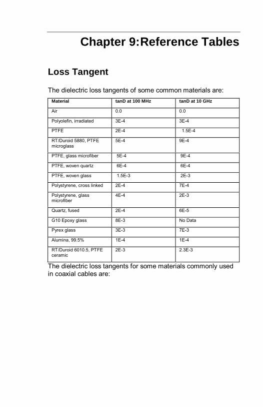
Chapter 9: Reference Tables
Loss Tangent
The dielectric loss tangents of some common materials are:Material tanD at 100 MHz tanD at 10 GHz
Air 0.0 0.0
Polyolefin, irradiated 3E-4 3E-4
PTFE 2E-4 1.5E-4
RT/Duroid 5880, PTFEmicroglass
5E-4 9E-4
PTFE, glass microfiber 5E-4 9E-4
PTFE, woven quartz 6E-4 6E-4
PTFE, woven glass 1.5E-3 2E-3
Polystyrene, cross linked 2E-4 7E-4
Polystyrene, glassmicrofiber
4E-4 2E-3
Quartz, fused 2E-4 6E-5
G10 Epoxy glass 8E-3 No Data
Pyrex glass 3E-3 7E-3
Alumina, 99.5% 1E-4 1E-4
RT/Duroid 6010.5, PTFEceramic
2E-3 2.3E-3
The dielectric loss tangents for some materials commonly usedin coaxial cables are:

Reference Tables
256
Material tanD at 100 MHz tanD at 3 GHz
Air 0.0 0.0
PTFE 2E-4 15E-4
PolyEthylene, DE-3401 2E-4 3.1E-4
Polyolefin, irradiated 3E-4 3E-4
Polystyrene 1E-4 3.3E-4
Polyvinal formal (Formvar) 1.3E-2 1.1E-2
Nylon 2E-2 1.2E-2
Quartz, fused 2E-4 6E-5
Pyrex Glass 3E-3 5.4E-3
Water, distilled 5E-3 1.6E-1
Note : This data is for solid materials. Foamed materials havelower loss tangents. These data are approximate. Consultmanufacturer for critical applications.
Metal Thickness
The thickness of the conductor metallization for planarstructures. The algorithms for microstrip are most accurate forthin metallization, but both loss and Zo are corrected forthickness.
For stripline, the algorithms are more accurate to thickermetallization. Thickness to 0.1*b or to the width is permissible.
Commonly used thicknesses:Metallization Type Thickness (mm) Thickness (mils)
½ ounce copper 0.018 0.71
1 ounce copper 0.036 1.42
2 ounce copper 0.072 2.83
Relative Dielectric Constants
Er is the substrate or dielectric constant, relative to free space.Following are constants of some common materials:
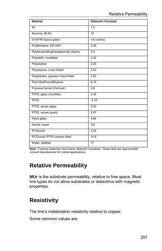
Relative Permeability
257
Material Dielectric Constant
Air 1.0
Alumina, 99.5% 10
G10/FR4 Epoxy glass 4.8 (varies)
PolyEthylene, DE-3401 2.26
Polyhexamethyleneadipamide (Nylon) 2.9
Polyolefin, irradiated 2.32
Polystyrene 2.53
Polystyrene, cross linked 2.53
Polystyrene, glassed cross linked 2.62
PolyTetraFluoroEthylene 2.10
Polyvinal formal (Formvar) 2.8
PTFE, glass microfiber 2.35
PTFE 2.10
PTFE, woven glass 2.55
PTFE, woven quartz 2.47
Pyrex glass 4.84
Quartz, fused 3.8
RT/Duroid 2.20
RT/Duroid, PTFE ceramic filled 10.5
Water, distilled 77
Note : Foamed materials have lower dielectric constants. These data are approximate;consult manufacturer for critical applications.
Relative Permeability
MUr is the substrate permeability, relative to free space. Mostline types do not allow substrates or dielectrics with magneticproperties.
Resistivity
The line’s metalization resistivity relative to copper.
Some common values are:
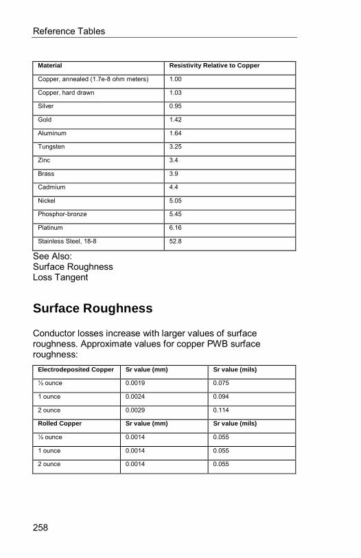
Reference Tables
258
Material Resistivity Relative to Copper
Copper, annealed (1.7e-8 ohm meters) 1.00
Copper, hard drawn 1.03
Silver 0.95
Gold 1.42
Aluminum 1.64
Tungsten 3.25
Zinc 3.4
Brass 3.9
Cadmium 4.4
Nickel 5.05
Phosphor-bronze 5.45
Platinum 6.16
Stainless Steel, 18-8 52.8
See Also:Surface RoughnessLoss Tangent
Surface Roughness
Conductor losses increase with larger values of surfaceroughness. Approximate values for copper PWB surfaceroughness:
Electrodeposited Copper Sr value (mm) Sr value (mils)
½ ounce 0.0019 0.075
1 ounce 0.0024 0.094
2 ounce 0.0029 0.114
Rolled Copper Sr value (mm) Sr value (mils)
½ ounce 0.0014 0.055
1 ounce 0.0014 0.055
2 ounce 0.0014 0.055
Chapter 10: S Parameters
Overview
The purpose of this chapter is to summarize network analysisconcepts and to define some of the parameters plotted by=SuperStar=.
Networks are considered as "black boxes". Because thenetworks are assumed to be linear and time invariant, thecharacteristics of the networks are uniquely defined by a set oflinear equations relating port voltages and currents. A number ofnetwork parameter types have been developed for this purpose,including H, Y, Z, S, ABCD, and others. These parameters maybe used to compute and display network responses and tocompute quantities useful for circuit design such as Gmax(maximum gain) and gain circles. Each parameter type hasadvantages and disadvantages. Carson [1] and Altman [2]provide additional information.
Introduction
S-parameters have earned a prominent position in RF circuitdesign, analysis, and measurement. Parameters used earlier inRF design, such as Y-parameters, require opens or shorts onports during measurement. This is a nearly impossible constraintfor high-frequency broadband measurements. Scatteringparameters [3, 4] (S-parameters) are defined and measured withthe ports terminated in a characteristic reference impedance.Modern network analyzers are well suited for measuring S-parameters. Because the networks being analyzed are oftenemployed by insertion in a transmission medium with a commoncharacteristic reference impedance, S-parameters have theadditional advantage that they relate directly to commonlyspecified performance parameters such as insertion gain andreturn loss.
Two-port S-parameters are defined by considering a set ofvoltage traveling waves. When a voltage wave from a source isincident on a network, a portion of the voltage wave istransmitted through the network, and a portion is reflected backtoward the source. Incident and reflected voltage waves mayalso be present at the output of the network. New variables are
S Parameters
260
defined by dividing the voltage waves by the square root of thereference impedance. The square of the magnitude of these newvariables may be viewed as traveling power waves.
|a1|2 = incident power wave at the network input|b1|2 = reflected power wave at the network input|a2|2 = incident power wave at the network output|b2|2 = reflected power wave at the network output
These new variables and the network S-parameters are relatedby the expressions:
b1 = a1S11 + a2S12
b2 = a1S21 + a2S22
S11 = b1/a1, a2 = 0
S12 = b1/a2, a1 = 0
S21 = b2/a1, a2 = 0
S22 = b2/a2, a1 = 0
Terminating the network with a load equal to the referenceimpedance forces a2 = 0. Under these conditions
S11 = b1/a1
S21 = b2/a1
S11 is then the network input reflection coefficient and S21 is thegain or loss of the network.
Terminating the network at the input with a load equal to thereference impedance and driving the network from the outputport forces a1 = 0. Under these conditions
S22 = b2/a2
S12 = b1/a2
S22 is then the network output reflection coefficient and S12 is thereverse gain or loss of the network.
Linear S-parameters are unitless. Since they are based onvoltage waves, they are converted to decibel format bymultiplying the log of the linear ratio by 20. It is not alwaysobvious whether an author is refering to linear or decibelparameters. To avoid this confusion, the book Oscillator Designand Computer Simulation and Versions 5.4 and earlier of=SuperStar= use C for linear S-parameters and S for the decibelform. This is somewhat unconventional. Version 6.0 and later of
Stability
261
GENESYS also supports the convention MAG[S21] which islinear and DB[S21] which is the decibel form. With reflectionparameters, the linear form is often refered to as a relectioncoefficient and the decibel form as return loss.
S11(dB)=input reflection gain=20 log S11
S22 (dB)=output reflection gain=20 log S22
S21(dB)=forward gain=20log S21
S12(dB)=reverse gain=20log S12
S21 and S12 are the forward and return gain (or loss) when thenetwork is terminated with the reference impedance. The gainwhen matching networks are inserted at the input, output, or bothis described later.
S11 and S22 coefficients are less than 1 for passive networks withpositive resistance. Therefore, the input and output reflectiongains, S11 and S22, are negative decibel numbers. ThroughoutEagleware material, the decibel forms S11 and S22 are referred toas return losses, in agreement with standard industryconvention. To be mathematically correct, they have been left asnegative numbers. As such, the rigorous convention would be tocall them return gain.
Input VSWR (VSWR1) and S11 are related by
VSWR1 = ( 1 + |S11| ) / ( 1 - |S11| )
The output VSWR is related to S22 by an analogous equation. Acircle of constant radius centered on the Smith chart is a circle ofconstant VSWR. The complex input impedance is related to theinput reflection coefficients by the expression:
I1 = Zo ( 1 + S11 ) / ( 1 - S11 )
The output impedance is similarly related to S22.
Stability
Because S12 of devices is not zero, a signal path exists from theoutput to the input. This feedback path creates an opportunity foroscillation. The stability factor, K, is
K = ( 1 - |S11|2 - |S22|2 + |D|2 ) / (2 |S12| |S21|)
where
D = S11S22 - S12S21
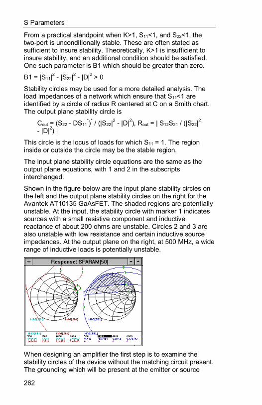
S Parameters
262
From a practical standpoint when K>1, S11<1, and S22<1, thetwo-port is unconditionally stable. These are often stated assufficient to insure stability. Theoretically, K>1 is insufficient toinsure stability, and an additional condition should be satisfied.One such parameter is B1 which should be greater than zero.
B1 = |S11|2 - |S22|2 - |D|2 > 0
Stability circles may be used for a more detailed analysis. Theload impedances of a network which ensure that S11<1 areidentified by a circle of radius R centered at C on a Smith chart.The output plane stability circle is
Cout = (S22 - DS11*)* / (|S22|2 - |D|2), Rout = | S12S21 / (|S22|2
- |D|2) |
This circle is the locus of loads for which S11 = 1. The regioninside or outside the circle may be the stable region.
The input plane stability circle equations are the same as theoutput plane equations, with 1 and 2 in the subscriptsinterchanged.
Shown in the figure below are the input plane stability circles onthe left and the output plane stability circles on the right for theAvantek AT10135 GaAsFET. The shaded regions are potentiallyunstable. At the input, the stability circle with marker 1 indicatessources with a small resistive component and inductivereactance of about 200 ohms are unstable. Circles 2 and 3 arealso unstable with low resistance and certain inductive sourceimpedances. At the output plane on the right, at 500 MHz, a widerange of inductive loads is potentially unstable.
When designing an amplifier the first step is to examine thestability circles of the device without the matching circuit present.The grounding which will be present at the emitter or source
Matching
263
should be included in the analysis. This stability data is used to1) add stabilizing components such as shunt input and outputresistors for bipolars or inductance in the source path forGaAsFETs and to 2) select an input and output matchingnetwork topology which properly terminates the device (at lowand high frequencies) for stability.
In the example above, matching networks with a small seriescapacitor adjacent to the device would insure capacitive loads atlow frequencies, thus enhancing stability. This is probablysufficient for the input. However, considering that device S-parameter data is approximate and since the output plane of thisdevice is more threatening, it would be prudent to stabilize thisdevice in addition to using series capacitors.
Note: Stability should be checked not only atthe amplifier operating frequencies, but alsoover the entire frequency range for which S-Parameter data is available.
Matching
One definition of network gain is the transducer power gain, Gt:Transducer power gain is the power delivered to the load dividedby the power available from the source.
Gt = P(delivered-to-load) / P(available-from-source)
Other gain definitions include the power gain, Gp, and theavailable power gain, Ga.
Gp = P(delivered-to-load) / P(input-to-network)
Ga = P(available-from-network) / P(available-from-source)
The S-parameter data for the network is measured with a sourceand load equal to the reference impedance. If the network is notterminated in the reference impedance, Gt can be computedfrom the reflection coefficients of the terminations on the networkand the S-parameters of the network. At this point we havemultiple sets of reflection coefficients: those of the terminationsand S11 and S22 of the network. To avoid confusion thetermination reflection coefficients are given a different symbol, G.
The transducer power gain with the network inserted in a systemwith arbitrary source and load reflection coefficients is [4]:
S Parameters
264
Gt = ( |S21|2 (1 - |Rs|2)(1 - |RL|2) ) / |(1 - S11RS)(1 - S22RL)- S21S12RLRS|2
where
RS = reflection coefficient of the sourceRL = reflection coefficient of the load
If and are both zero, then
Gt=S21
or
Gt(dB)=20log S21=S21(dB)
Therefore, when a network is installed in a system with sourceand loads equal to the reference impedance, S21 is the networktransducer power gain in decibels.
Because S11 and S22 of a network are not in general zero, aportion of the available source power is reflected from thenetwork input and is dissipated in the source. The insertion of alossless matching network at the input (and/or output) of thenetwork could increase the gain of the overall system ifreflections toward the source were reduced. Shown below is atwo-port network with lossless matching networks insertedbetween the network and the source and load.
GMAX and MSG
When the input and output networks are simultaneouslydesigned for maximum gain, there is no reflection at the sourceor load. The maximum transducer power gain, Gmax, is given by
Gmax = ( |S21| / |S12| ) * (K - sqrt(K2 - 1))
The maximum stable gain, MSG, is defined as Gmax with K=1.Therefore
MSG = |S21| / |S12|
A GENESYS plot of GMAX shows Gmax when K>1 and MSGwhen K<1.
Again, acheiving this maximum gain requires that the inputnetwork is designed such that RS is the complex conjugate of S11and RL is the complex conjugate of S22. GENESYS returns therequired reflection coefficients, impedance and admittance forthe input and output networks as GM1, GM2, ZM1, ZM2, YM1and YM2, respectively.
The Unilateral Case
265
The Unilateral Case
Historically, to simplify the complex equation for Gt in theprevious section on matching, S12 was set to zero. At higherfrequencies, where the device S12 is typically larger, thisassumption is less valid. The assumption simplifies manual andgraphical design but is unnecessary in modern computer-assisted design. The assumption also allows factoring the aboveequation into terms that provide insight into the design process.If S12 =0, then
Gtu = ( |S21|2 (1 - |Rs|2)(1 - |RL|2) ) / |(1 - S11RS)(1 -S22RL)|2
where
Gtu=unilateral transducer power gain
When both ports of the network are conjugately matched, andS12 = 0,
Gtu = |S21|2 / ( (1 - |S11|2)(1 - |S22|2) )
The first and third terms indicate the gain increase achievable bymatching the input and output, respectively. If S11 or S22approach 1, substantial gain improvement is achieved bymatching. Matching not only increases the network gain, butreduces reflections from the network.
When network gain flatness across a frequency band is moredesirable than minimum reflections, the lossless matchingnetworks are designed to provide a better match at frequencieswhere the two-port gain is lower. By careful design of amplifiermatching networks, it is possible to achieve a gain response flatwithin fractions of a decibel over a bandwidth of an octave ormore.
Gain Circles
When the device is complex conjugately matched, thetransducer gain is Gmax and if the device is terminated with thesame resistance used to measure the device S-parameters thetransducer gain is S21. The gain with arbitrary terminations canbe visualized on the Smith chart using gain circles.
=SuperStar= plots three forms of gain circles: transducer gainunilateral circles, GU1 for the input network and GU2 for the
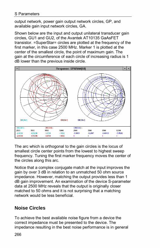
S Parameters
266
output network, power gain output network circles, GP, andavailable gain input network circles, GA.
Shown below are the input and output unilateral transducer gaincircles, GU1 and GU2, of the Avantek AT10135 GaAsFETtransistor. =SuperStar= circles are plotted at the frequency of thefirst marker, in this case 2500 MHz. Marker 1 is plotted at thecenter of the smallest circle, the point of maximum gain. Thegain at the circumference of each circle of increasing radius is 1dB lower than the previous inside circle.
The arc which is orthogonal to the gain circles is the locus ofsmallest circle center points from the lowest to highest sweepfrequency. Tuning the first marker frequency moves the center ofthe circles along this arc.
Notice that a complex conjugate match at the input improves thegain by over 3 dB in relation to an unmatched 50 ohm sourceimpedance. However, matching the output provides less than 1dB gain improvement. An examination of the device S-parameterdata at 2500 MHz reveals that the output is originally closermatched to 50 ohms and it is not surprising that a matchingnetwork would be less beneficial.
Noise Circles
To achieve the best available noise figure from a device thecorrect impedance must be presented to the device. Theimpedance resulting in the best noise performance is in general
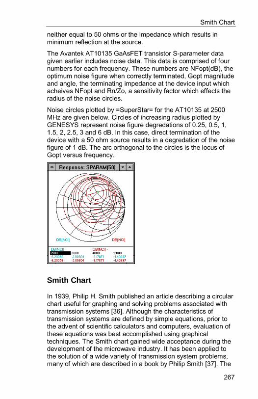
Smith Chart
267
neither equal to 50 ohms or the impedance which results inminimum reflection at the source.
The Avantek AT10135 GaAsFET transistor S-parameter datagiven earlier includes noise data. This data is comprised of fournumbers for each frequency. These numbers are NFopt(dB), theoptimum noise figure when correctly terminated, Gopt magnitudeand angle, the terminating impedance at the device input whichacheives NFopt and Rn/Zo, a sensitivity factor which effects theradius of the noise circles.
Noise circles plotted by =SuperStar= for the AT10135 at 2500MHz are given below. Circles of increasing radius plotted byGENESYS represent noise figure degredations of 0.25, 0.5, 1,1.5, 2, 2.5, 3 and 6 dB. In this case, direct termination of thedevice with a 50 ohm source results in a degredation of the noisefigure of 1 dB. The arc orthogonal to the circles is the locus ofGopt versus frequency.
Smith Chart
In 1939, Philip H. Smith published an article describing a circularchart useful for graphing and solving problems associated withtransmission systems [36]. Although the characteristics oftransmission systems are defined by simple equations, prior tothe advent of scientific calculators and computers, evaluation ofthese equations was best accomplished using graphicaltechniques. The Smith chart gained wide acceptance during thedevelopment of the microwave industry. It has been applied tothe solution of a wide variety of transmission system problems,many of which are described in a book by Philip Smith [37]. The
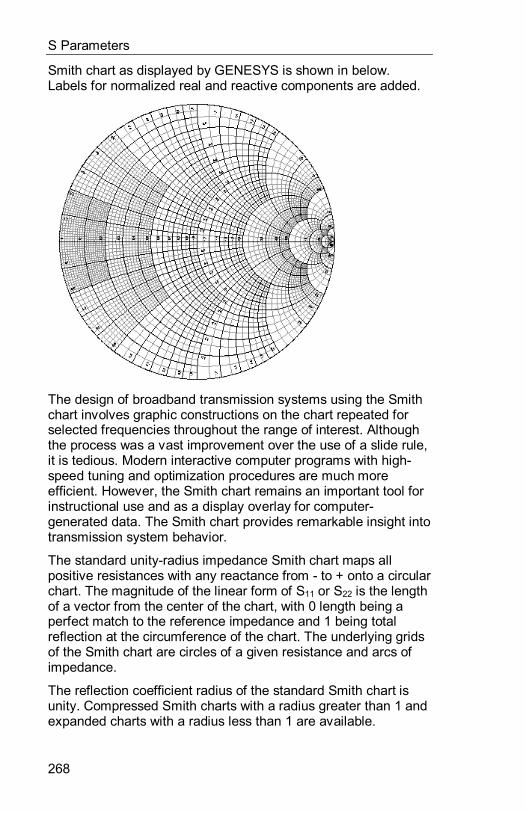
S Parameters
268
Smith chart as displayed by GENESYS is shown in below.Labels for normalized real and reactive components are added.
The design of broadband transmission systems using the Smithchart involves graphic constructions on the chart repeated forselected frequencies throughout the range of interest. Althoughthe process was a vast improvement over the use of a slide rule,it is tedious. Modern interactive computer programs with high-speed tuning and optimization procedures are much moreefficient. However, the Smith chart remains an important tool forinstructional use and as a display overlay for computer-generated data. The Smith chart provides remarkable insight intotransmission system behavior.
The standard unity-radius impedance Smith chart maps allpositive resistances with any reactance from - to + onto a circularchart. The magnitude of the linear form of S11 or S22 is the lengthof a vector from the center of the chart, with 0 length being aperfect match to the reference impedance and 1 being totalreflection at the circumference of the chart. The underlying gridsof the Smith chart are circles of a given resistance and arcs ofimpedance.
The reflection coefficient radius of the standard Smith chart isunity. Compressed Smith charts with a radius greater than 1 andexpanded charts with a radius less than 1 are available.
Smith Chart
269
High impedances are located on the right portion of the chart,low impedances on the left portion, inductive reactance in theupper half, and capacitive reactance in the lower half. Realimpedances are on a line from the left to right, and purelyreactive impedances are on the circumference. The angle of thereflection coefficient is measured with respect to the real axis,with zero degrees to the right of the center, 90o straight up, and -90o straight down.
The impedance of a load as viewed through an increasing lengthof lossless transmission line, or through a fixed length withincreasing frequency, rotates in a clockwise direction withconstant radius when the line impedance equals the referenceimpedance. If the line and reference impedances are not equal,the center of rotation is not about the center of the chart. Onecomplete rotation occurs when the electrical length of the lineincreases by 180o. Transmission line loss causes the reflectioncoefficient to spiral inward.
The length of a vector from the center to a given point on theSmith chart is the magnitude of the reflection coefficient. Theangle of that vector with respect to the real axis to the right is thephase angle of the reflection coefficient. Several commondefinitions are used to represent the length of this vector. Theyare referred to as radially scaled parameters because they relateto a radial distance from the center towards the outside circle ofthe chart.

Chapter 11: Device Data
Overview
Within GENESYS are a wide range of element models. Also, themodel and equation features provide for user creation of models.However, it is often necessary or desirable to characterize adevice used in GENESYS by measured or externally computeddata. This function is provided for by the use of the ONE, TWO,THR, FOU, and NPO elements which read S, Y, G, H, or Z-parameter data.
Because =SuperStar= is a linear simulator, and because circuitsare assumed time-invariant (element values are not a function oftime), sub-components are uniquely defined by a set of portparameter sets, such as two-port S-parameter data.
Although ONE, TWO, THR, FOU, and NPO are typically used foractive devices, they may be used for any devices for which youcan compute or measure data. For example, they could be usedto characterize an antenna, a circuit with specified group delaydata, or measured data for a broadband transformer or a pad.
Using a Data File in GENESYS
Data files can be used in GENESYS in two different ways:
y By adding a Link to a Data File in a simulation. Thisallows measurements to refer directly to the data filewithout the need to create a design.
y By using ONE, TWO, THR, FOU, or NPO elementsin a circuit file or schematic.
In both cases, you must know in advance how many ports thedevice data represents. For transistors, this is almost always 2.
Provided Device Data
GENESYS includes over 25,000 data files for many differentdevice types. Device data was provided directly by themanufacturers in electronic format.

Device Data
272
Note: Eagleware could not test every file thatwas provided. Through random sampling, weedited errors found in some files. It is theuser’s responsibility to test each file foraccuracy.
Creating New Data Files
You may easily add other devices to the library using the editorin =SuperStar= to simply type the data into a file with the nameof your choice. From the =SuperStar= Menu, select File/New andchoose Text. Type in the data, and when you have finished,select File/Save. The file format is standard ASCII.
The first line in the file after any initial comments is a formatspecifier in the form:
# units type format R impedance
where:
units is either Hz, kHz, MHz, or GHztype is the type of the data file, either S, Y, G, H, or Zformat is DB for dB/angle data, MA for linearmagnitude/angle data, or RI for real/imaginary dataimpedance is the reference impedance in ohms,commonly 50 or 75
One of the most common format specifiers is:
# MHZ S MA R 50
This indicates that the data is in S parameter form normalized to50 ohms. The data is given in linear polar format (magnitude &angle). The frequencies are in megahertz.
The data follows after the format specifier. A typical line for thistwo-port file is:
500 .64 -23 12.5 98 .03 70 .8 -37
In this case, 500 is the frequency in megahertz. The magnitudesof S11, S21, S12 and S22 are .64, 12.5, .03 and .8, respectively.The phases are -23, 98, 70 and -37 degrees, respectively.
Alternatively, Y-parameter data may be used. The formatspecifier could be:
# GHZ Y RI R 1
File Record Keeping
273
This would indicate rectangular, unnormalized Y parameter datawith frequencies in GHz. A typical line is:
30 0 3E-4 9E-3 -8E-3 2E-5 0 -1E-4 1E-3
In this case, the frequency in gigahertz is 30. The real values ofY11, Y21, Y12 and Y22 are 0, 9E-3, 2E-5 and -1E-4 mhos,respectively. The imaginary values are 3E-4, -8E-3, 0 and 1E-3mhos, respectively.
A sample S-parameter data file is shown below. The only portionof the file required for GENESYS is the segment in the middlewith frequencies and S-parameter data. Lines in the data filebeginning with "!" are comments and are ignored. The noise dataat the end of the file is used for noise figure analysis. (Noise isdiscussed in a later section.)! AT41435 S AND NOISE PARAMETERS! Vce=8V Ic=10mA! LAST UPDATED 06-1-89# GHZ S MA R 50!FREQ S11 S21 S12 S220.1 .80 -32 24.99 157 .011 82 .93 -120.5 .50 -110 1 2.30 108 .033 52 .61 -281.0 .40 -152 6.73 85 .049 56 .51 -301.5 .38 176 4.63 71 .063 59 .48 -322.0 .39 166 3.54 60 .080 58 .46 -372.5 .41 156 2.91 53 .095 61 44 -403.0 .44 145 2.47 43 .115 61 .43 -483.5 .46 137 2.15 33 .133 58 .43 -584.0 .46 127 1.91 23 .153 53 .45 -684.5 .47 116 1.72 13 .178 50 .46 -755.0 .49 104 1.58 3 .201 47 .48 -826.0 .59 81 1.34 -17 .247 36 .43 -101!FREQ Fopt GAMMA OPT RN/Zo0.1 1.2 .12 3 0.170.5 1.2 .10 14 0.171.0 1.3 .05 28 0.172.0 1.7 .30 -154 0.164.0 3.0 .54 -118 0.35
File Record Keeping
Most device files provided with GENESYS are S-parameter filesin the usual device configuration, typically common emitter orcommon source. Devices you add to the library may use theground terminal of your choice. However, if you always keepdata in a consistent format, record keeping chores are greatlyminimized.
Device Data
274
Exporting Data Files
"Export/S-Parameters" in the File menu writes S-parameter datafrom any simulation or data source. This output data file hasexactly the same format as S-parameter files used to importdata. This allows the user to analyze, tune and optimize sub-networks which are then stored as S-parameter data files for uselater in other circuit files. The S-parameter data file written byGENESYS has one line of data for each simulation frequency. Ifthere are two or more available simulations or designs in thecircuit file, GENESYS displays a dialog box to allow you to selectthe simulation or design to use.
Note: To avoid confusion, we recommendyou use the .OUT extension for naming allyour output data files.
Noise Data in Data Files
Some of the data files provided with GENESYS also includenoise data used for noise figure analysis. This data includes theoptimum noise figure (NFopt), the complex source impedance topresent to the device to achieve the optimum noise figure (Gopt),and the effective noise resistance (Rn). Example data can beseen in the data file previously shown in Creating New DataFiles.
The best noise figure in a circuit is achieved when the device ispresented with an optimum source impedance. The optimuminput network to achieve this objective does not in general resultin an excellent return loss match. Balanced amplifiers andisolators are sometimes used to achieve both the optimum noisefigure and a good match.
Losses in the input network, feedback networks around thetransistor, emitter feedback and multiple stages all effect thenoise figure of the circuit. All of these effects are accuratelysimulated in GENESYS using the noise correlation matrixtechnique [5,6].
Chapter 12: References
GENESYS References
[1] Ralph S. Carson, High-Frequency Amplifiers, John Wiley &Sons, New York, 1982.
[2] Jerome L. Altman, Microwave Circuits, D. Van Nostrand,Princeton, NJ, 1964.
[3] Application Note 95, S-Parameters-Circuit Analysis andDesign, Hewlett-Packard, Palo Alto, CA, September 1968.
[4] Application Note 154, S-Parameter Design, Hewlett-Packard,Palo Alto, CA, April 1972.
[5] V. Rizzoli and A. Lipparini, "Computer-Aided Noise Analysisof Linear Multiport Networks of Arbitrary Topology," IEEE Trans.MTT-33, No. 12, December 1985.
[6] H. Hillbrand and P. Russer, "An Efficient Method forComputer Aided Nose Analysis of Linear Amplifier Networks,"IEEE Trans. Circuits Syst., Vol. CAS-23, April 1976.
[7] H.A. Watson, ed., Microwave Semiconductor Devices andTheir Circuit Applications, McGraw-Hill, New York, 1969, pp.271-278.
[8] Lloyd P. Hunter, ed., Handbook of SemiconductorElectronics, 3rd edition, McGraw-Hill, New York, 1970, pp. 11-3to 11-19.
[9] H.E. Green, "The Numerical Solution of Transmission LineProblems," Advances in Microwaves, Vol. 2, Academic Press,New York, 1967, pp. 327-393.
[10] K.C. Gupta, et al., Computer-Aided Design of MicrowaveCircuits, Artech House, Dedham, Massachusetts, 1981, pp. 131-134.
[11] P.I. Somlo, "The Computation of Coaxial Line StepCapacitances," IEEE Trans. MTT, Vol MTT-15, January 1967,pp. 48-53.
[12] W. Alan Davis, Microwave Semiconductior Circuit Design,Van Nostrand Reinhold, New York, 1984, pp. 118-119.
References
276
[13] P. Wolf, "Microwave Properties of Schottky-barrier Field-effect Transistors," IBM Journal of Research and Development,March 1970, pp. 125-141.
[14] "Device Modeling," Avantek Microwave Semiconductors:GaAs and Silicon Products, Avantek, Santa Clara, 1989, pp. 8-12 to 8-13.
[15] M. Kirshning, et al., "Measurement and Computer-AidedModeling of Microstrip Discontinuities by an Improved ResonatorMethod," MTT-S Digest, 1983, pp. 495-497.
[16] M. Kirshning, et al., "Accurate Wide-Range DesignEquations for the Frequency Dependent Characteristics ofParallel Coupled Microstrip Lines," IEEE MTT-32, 1984, pp. 83-90. Errata, MTT-33, 1985, p. 288.
[17] Rolf H. Jansen, "High-Speed Computation of Single andCoupled Microstrip Parameters Including Dispersion, High-OrderModes, Loss and Finite Strip Thickness," MTT-26, 1978, pp. 75-81.
[18] M.V. Schneider, "Microstrip Lines for Microwave IntegratedCircuits," The Bell System Technical Journal, May-June 1969,pp. 1421-1444.
[19] E.O. Hammerstad, "Equations for Microstrip Circuit Design,"Proc. 5th European Microwave Conference, Hamberg, 1975, pp.268-272.
[20] P. Benedek and P. Silvester, "Equivalent Capacitance forMicrostrip Gaps and Steps," IEEE MTT-20, November, 1972, pp.729-733.
[21] R. Jansen and M. Kirschning, "Arguments and an AccurateModel for the Power-Current Formulation of MicrostripCharacteristics Impedance," AEU, Band 37, 1983, Heft 3/4, pp.108-112.
[22] Harold A. Weeler, "Transmission-Line Properties of a Stripon a Dielectric Sheet on a Plane," IEEE MTT-25, 1977, pp. 631-647.
[23] H. Atwater, "Microstrip Reactive Circuit Elements," IEEEMTT-31, June 1983, pp. 488-491.
[24] J.P. Vinding, "Radial Line Stubs as Elements in StriplineCircuits," NEREM Rec., pp. 108-109, 1967.
GENESYS References
277
[25] A. Farrar and A.T. Adams, "Matrix Methods for MicrostripChange in Width and Cross-Junctions," IEEE MTT-20, August1972, pp. 497-504.
[26] A. Gopinath, "Equivalent Circuit Parameters of MicrostripChange in Width and Cross-Junctions," IEEE MTT-24, March1976, pp. 142-144.
[27] M.E. Goldfarb and R.A. Pucel, "Modeling Via Hole Groundsin Microstrip," IEEE Microwave and Guided Wave Letters, Vol. 1No. 6, June 1991, pp. 135-137.
[28] G.B. Stracca, G. Macchiarella and M. Politi, "NumericalAnalysis of Various Configurations of Slab Lines," MTT-34, No.3, March 1986, p. 359-363.
[29] H.M. Altschuler and A.A. Oliner, "Discontinuities in theCenter Conductor of Symmetric Strip Transmission Line" IREMTT-8, May 1960, pp. 328-339.
[30] Seymour B. Cohn, "Shielded Coupled-Strip TransmissionLine," MTT-3, 1955, pp. 29-38.
[31] S.B. Cohn, "Characteristic Impedance of Shielded StripTransmission Line," MTT-2, 1954, pp. 52-55/
[32] H.A. Wheeler, "Transmission Line Properties of a StriplineBetween Parallel Planes," MTT-26, 1978, pp. 866-876.
[33] I.J. Bahl and R.Garg, "A Designer's Guide to StriplineCircuits," Microwaves, Jan. 1978, pp. 90-96.
[34] Private phone conversation between R.W. Rhea and I.J.Bahl, October 1987.
[35] N. Marcuvitz, Waveguide Handbook, Peter Peregrinus Ltd.,London, 1986.
[36] Phillip H. Smith, "Transmission Line Calculator," Electronics,Vol. 12, Jamuary 1994, p. 29.
[37] Phillip H. Smith, Electronic Applications of the Smith Chart,2nd edition, Noble Publishing, Atlanta, 1995.
[38] Guillermo Gonzales, Microwave Transistor Amplifiers:Analysis and Design, 2nd edition, Prentice-Hall, New York, 1997.
[39] H.C. Miller, "Inductance Formula for a Single-Layer CircularCoil," Proc. IEEE, Vol. 75, pp. 256,257, 1987.
[40] R.G. Medhurst, "H.F. Resistance and Self-Capacitance ofSingle-Layer Solenoids," Wireless Engineer, pp. 80-92, 1947.

References
278
[41] C.A. Balanis, Antenna Theory: Analysis & Design, JohnWiley & Sons, New York, 1982, pp. 292-295.
[42] A. Weisshaar and V.K. Tripathi, "Perturbation Analysis andModeling of Curved Microstrip Bends," IEEE MTT, Vol. 38(10),1990, pp. 1449-1454.
[43] S.S. Gevorgian, et.al., "CAD Models for MultilayeredSubstrate Interdigital Capacitors," IEEE MTT-44, 1996, pp. 896-904.
[44] F.W. Grover, Inductance Calculations, Dover Publications,Inc., New York, 1962.
[45] J.I. Smith, "The Even- and Odd-Mode CapacitanceParameters for Coupled Lines in Suspended Substrate," IEEEMTT-19, 1971, pp. 424-431.
[46] R.L. Remke and G.A. Burdick, "Spiral Inductors for Hybridand Microwave Applications," Proc. 24th Electron ComponentsConf., 1974, pp. 152-161.
[47] C.R. Burrows, "The Exponential Transmission Line," BellSystem Technical Journal, Vol. 37, 1938, pp. 555-573.
[48] R.E. Collin, Field Theory of Guided Waves, McGraw-Hill,New York, 1960, pp. 185-195.
[49] H.M. Greenhouse, "Design of Planar RectangularMicroelectronic Inductors," IEEE Trans. Parts, Hybrids, andPackaging, PHP-10(2), June 1974, pp. 101-109.
[50] B.C. Wadell, Transmission Line Design Handbook, ArtechHouse, Boston, 1991.
[51] C.L. Ruthroff, "Some Broad-Band Transformers," Proc. IRE,Vol. 47, 1959, pp. 1337-1342.
[52] D.M. Krafcsik and D.E. Dawson, "A Closed-FormExpression for Representing the Distributed Nature of the SpiralInductor," 1986 Microwave and Millimeter-Wave MonolithicCircuits Symposium, 1986, pp. 87-92.
Index
11-Port Data File , 64
22-port , 1212-Port Data File , 113
33-Port Data File , 101
990 Degree Line , 161
AABC , 12ABCD , 12, 259ABS , 132AC, 161Actions Menu , 152Adding , 271
Link , 271Admittance , 121, 217, 264Air Above , 206Air Below , 206Air core inductor , 13AIRIND1, 13Allow Multiple Open
Workspaces , 169ANG, 123, 132ANG360, 123, 132Angle , 123Aperture List , 174, 175
Editing , 175Arc Object , 185ARCCOS, 132ARCCOSH, 132ARCSIN, 132ARCSINH, 132ARCTAN , 132ARCTANH , 132
Array Index , 131Arrays , 131, 132, 136, 138ASCII, 63, 113ASCII Drill List , 147Assembly , 204Associations , 203Asymmetrical , 56ATN, 132Auto-Replace Tuned Values ,
169Available Footprints , 182
BB1, 121, 261Balanced amplifiers , 274BASE , 127Bends , 81BESSELJ0 , 132BIP, 14Bipolar transistor model , 14Bitmap , 147Bond-wire inductances , 31Bottom Cover , 200, 206Box Height , 200Box Settings , 200Box Width , 200Built-in Functions , 132, 138Bulk Conductivity , 206BYREF, 142
CCalling C/C++ Programs , 143CAP, 16Capacitors , 16CCC, 17CCV, 18CEN, 19Center Selected On Page ,
155CGA, 20Chamfered , 38Change Footprint , 186CIR3, 21Circles , 121, 124, 259, 261,
266, 267
Index
280
CLI, 22CLI4, 23Close Workspace , 147Closed Loop , 179Coax Toolbar , 165Coaxial center conductor
gap , 20Coaxial conductor step , 27Coaxial End , 19Combline , 25, 39, 76, 82COMPLEX, 132Component Object , 186Components , 211Concatenation , 135Conducting Wire , 118Connect Selected Parts , 155Connections , 182Constants , 121, 135Copper , 257Copy , 149COS, 132COSH, 132Co-simulation , 220COUNT, 132, 136, 138Coupled lines , 24Coupled Microstrip Lines , 41Coupled Slabline , 77Coupled striplines , 83CPL, 24, 25CPN, 25Create Mask , 191Creating , 33, 63, 101, 113,
272four-port , 33New Data Files , 272n-port , 63three-port , 101two-port , 113
CST, 27Current controlled current
source , 17Current controlled voltage
source , 18Current Dir , 187Custom Aperture List dialog ,
174Custom Apertures , 176Cut , 149
DData File , 224, 271, 274DB, 121, 123, 272DB Magnitude , 124DB/angle , 272DB10, 132DB20, 132DBANG , 121, 123DBANG360, 123DBMAG , 121DC, 161D-code identifier , 175Decomposition , 220Default Footprint , 203Default Operator , 121, 123Default Simulation/Data , 124,
215, 216, 217, 218, 227Default Viahole Layers , 200DELAY , 29Delete Layer , 204Device Toolbar , 163Dielectric , 255Dielectric Const , 226Dielectric Constant , 256Dim , 138Dimensions , 226DIPOLE, 30Dipole antenna , 30Disable All Simulations , 169Dispersion , 48Distortionless TEM
Transmission Line , 106Distributed RC , 164Distributed RC Transmission
Line , 75Distribution , 228DLLs , 143Draw Size , 187, 194Drill Diameter , 198Drill List , 147Drop Trailing Zeros , 169DTOR, 135Duplicate , 149DXF File, 147DXF Setup , 173
Index
281
EEdit Menu , 149Edit substrate , 226Element Z-Ports , 206Elements , 9EMport , 160, 220EMPort Object , 187EPS0, 135Equality Check , 131Equations , 123, 124, 125,
131, 132, 136, 138, 142,218, 227
Equivalence , 131Errors Window , 150, 159ETA0, 135Etch Factor , 204Excellon , 147Exclusive-OR , 141EXP, 132EXP1, 135Exponential Notation Above ,
169Exponential TEM
Transmission Line , 108Exponentiation , 131Export/DXF File , 173Export/Gerber File , 174Export/HPGL File , 178Exporting , 147, 154, 274
ASCII, 147Data Files , 274Excellon , 147SPICE file , 154Touchstone file , 147
Expression , 132Extrapolate , 33, 63, 64, 101,
113, 138
FFET transistor model , 31FIX, 132FN_E, 132FN_K, 132Font , 197Fonts , 210Footprint Editor , 153, 186
Footprint Library Selector ,182
Footprints , 153, 194, 200, 203FOU, 33, 271Four Terminal coaxial line ,
23Four-Port Data , 33FREQ, 138Frequencies , 219FUNCTION, 127, 142
GGA, 263, 265GA Circles , 121GAIN, 34Gain Circles , 121, 259, 265Gap, 87Gaussian , 228GD, 123General Layer , 204, 206General Layer Tab , 206General Options , 169Generalized S-Parameters ,
220Generate Custom Apertures ,
174, 175Generate Viewer Data , 220Gerber , 147, 174, 176Gerber File , 147, 176Gerber Setup dialog , 175GET, 132GETINDEPVALUE , 132, 138GETVALUE , 132, 138GETVALUEAT , 132, 138Global Options , 171Global Units , 145GM, 123GM1, 264GM2, 264GMAX, 121, 123, 259, 264,
265GMi, 121GOPT, 121, 123, 274GOTO, 127GP, 263, 265GP Circles , 121Graph Properties , 215
Index
282
Graph Toolbar , 160Greater Than , 131Grid , 200, 211Grid Density , 211, 217Grid Spacing , 200Grid Spacing Y , 200Grid Style , 200Ground Plane , 195, 206Grounded Input , 179Ground-plane , 191, 198, 206Group Object , 189Gt, 263GU1, 265GU1 Circles , 121GU2, 265GU2 Circles , 121GYR, 35Gyrator , 35
HH Parameters , 121Height , 145, 226Hide Silk Layers , 186Higher resolution , 181HPGL file , 147, 178Hyperbolic , 132
IIdeal delay block , 29Ideal gain block , 34Ideal isolator , 37Ideal monopole , 49Ideal Phase Shift , 68Ideal Transformer , 110, 111IF, 127IF THEN GOTO Statement ,
127, 141IFF, 132, 138IF-THEN statements , 138IFTRUE, 132, 138IM, 123, 132IMAG, 132IMP, 141Impedances , 121, 264, 267Implication , 131Import 6.x Model Library , 147
IND, 36Inductor , 36Inner Diameter , 191Input VSWR , 259Insert Layer , 204INT, 132Integer Division , 131Interdigital , 25, 39, 76, 82Interdigital Capacitor , 47Internal Ports , 187Interpolate , 33, 63, 64, 101,
113, 138, 220ISOLATOR, 37
JJunction Circle Size , 171
KKeep Away , 195
LLABEL , 127Layout Menu , 155Layout Toolbar , 160Leading Digits , 174Less Than , 131, 132Line button , 200Line Direction , 187Line Object , 190Line Width , 160, 190, 200Linear Magnitude , 124Linear Measurements , 121Linear Simulation Properties ,
219Linear S-parameters , 259Link , 224, 271LN, 132LN2, 135Load Footprint , 153Load From Layer File , 204Load From Library , 226Loaded Q , 123, 124LOG, 132Logical Operators , 141Loss Tangent , 206, 226, 255
Index
283
Lumped capacitance , 16Lumped resistance , 78Lumped Toolbar , 162
MMA, 272MAG, 123, 132MAGANG , 121, 123MAGANG360 , 123Magnetic Wall , 206Main GENESYS Toolbar , 159Make Tunable , 154Marcuvitz , 117Matrices , 136MATRIX, 132MAX, 132Max Critical Freq , 220MBN, 38MCN, 39MCP, 41MCR, 42MCURVE, 44Measurements , 121, 123, 124,
125, 132, 138, 215, 216,218, 227, 259
Measuring , 259S-parameters , 259
MEN, 45Merge Footprint , 153Metal , 206Metal Thickness , 226, 256Metalization resistivity , 257MGA, 46Microstrip , 206Microstrip Bend , 38Microstrip Cross , 42Microstrip Curved Bend , 44Microstrip Gap , 46Microstrip Interdigital
Capacitor , 47Microstrip Line , 48Microstrip Linearly Tapered
Line , 58Microstrip Open End , 45Microstrip Radial Stub , 52Microstrip Rectangular
Inductor , 50
Microstrip Spiral Inductor , 54Microstrip Step , 56Microstrip Tee Junction , 59Microstrip Toolbar , 165Microstrip Via Hole , 61MIDCAP, 47Min
Max, 227MIN, 132Mirror , 149MLI, 48MMTLP, 90Model , 9Model Properties , 214Modify Footprint Library , 153MONOPOLE, 49Monopole Antenna , 49Monte Carlo , 152, 228MRIND, 50MRS, 52MSG, 264MSPIND, 54MST, 56MTAPER, 58MTE, 59MU0, 135MUI, 60Multi Place Parts , 200Multi-dimensional , 138Multi-mode , 90, 187, 220Multi-Page Output , 178, 181Multiple coupled , 25Multiple Coupled Microstrip
Lines , 39Multiple Coupled Rods , 76Multiple Coupled Striplines ,
82Multiplication , 131Multiplier , 135MUr, 257Mutually Coupled Inductors ,
60MVH, 61
NNCI, 124NCI Circles , 121
Index
284
NET, 62NET Block , 62Netlist , 9New Data Files , 272
Creating , 272New Footprint , 153NF, 121, 123NFMIN, 121, 123NFopt , 274NFT, 121NMEAS, 121, 123Noise Circles , 121, 124, 266Noise correlation , 121, 274Noise Data , 274Non-deembedded , 187Normal Distribution , 228Normalized , 220, 272NOT, 141NPO, 271NPOn, 63N-Port Data File , 63Number Format , 174
OObject Dimensions , 200Omit Leading Zeros , 174Omit Trailing Zeros , 174ONE, 64, 271One-port , 206One-port S-Parameter , 64OPA, 65Operational amplifiers , 65Operations , 138Operator descriptions , 131Operators , 123, 124, 131, 135,
136, 141, 227Optimal admittance , 121Optimization , 121, 124, 152,
227Optimization Target dialog ,
227Optimization Targets , 180,
227Optimization Targets On
Graphs , 169OR, 141Origin , 155, 200
Orthogonal Mode , 190Oscillator Design , 259Out-of-bounds , 136Output Aperture List , 174Output Equations , 138
PPad Diameter , 191Pad Height , 191Pad Object , 191Pad Shape , 191, 198Pad Width , 191Page Height , 211Page Width , 211Parallel L-C resonator , 66, 67Parameter Sweep Properties ,
225Parameters , 121Parasitics , 212Part Constrain Angle , 149,
171Paste, 149Percentage , 228Permeability , 257Permittivity , 206PFC, 66PFL, 67PHASE, 68Physical Desc , 206PI, 135Piezoelectric resonator , 120PIN, 69Place Footprint Port , 155PLC, 71Polar Chart Properties , 216Polygon Fill Min Aperture
Diameter , 174Polygon Object , 193Port Impedance , 220Port Number , 194Port Object , 194Port Size , 200Post-processing , 121, 123,
124, 125, 132, 138Pour Object , 195PRC, 72Precedence , 131
Index
285
Print Preview , 147Print Quality , 181Print Setup , 181PRL, 73Probability , 228Probability distribution , 228Provided Device Data , 271PRX, 74
QQL, 123
RRadians multiplier , 135Random Number Seed , 228Raster Scan , 174RCLIN, 75RCN, 76RCP, 77RE, 123, 132REAL , 132Record Keeping , 273RECT, 121, 123Rectangle Object , 196Rectangular , 191Rectangular Waveguide Line ,
119Rectangular waveguide-to-
TEM, 117Rectangular Wire , 79Redo , 149, 159REF, 127Reference Plane , 187Reflection Coefficient , 259,
263, 264, 267Relational , 141Relative Dielectric
Constants , 206, 256Relative Permeability , 257Renumber Nodes , 154RES, 78Reset Defaults , 186Resistance , 121Resistivity , 206, 226, 257Resistor , 78Resolution , 181
RETURN, 127, 142RI, 272RIBBON, 79RLI, 80RN, 121, 274RND, 132Rotate , 149Roughness , 206, 226Round , 191Rounded Ends , 185, 190Rounded/square , 160RTOD, 135Rubber Bands , 182, 200Rubber-bands , 200Ruthroff transformer , 112
SS Parameters , 121, 124Sample Expressions , 132Sample Measurements , 124Samples , 228Save, 147Save Footprint , 153Save Layout As Footprint ,
155SB1 Circles , 121SB2 Circles , 121SBN, 81Scalar/matrix combination ,
136Schematic Menu , 154Schematic Part Layout
Options , 212Schematic Properties , 211SCN, 82SCP, 83Select All , 149Semi-Infinite Waveguide , 206SEN, 84Sensitivity , 152, 266Sensitivity Analysis , 152Series inductor , 88Series L-C , 85, 86Setup Variables , 228SFC, 85SFL, 86SGA, 87
Index
286
Show =EMPOWER= , 200Show Box , 200Show Data Points on New
Graphs , 169Show Drill Holes , 173, 178,
181Show grid , 171Show Grid Dots , 200Show SPICE Details , 171Show Yield Targets On
Graphs , 169Sigma , 206, 228Silk , 186, 204Simulation , 124Simulation/Data , 124SIN, 132Single-mode , 90SINH, 132Slabline , 76, 80Slabline Toolbar , 166SLC, 86, 88SLI, 89SmartScan , 174Smith Chart , 121, 124, 267Smith Chart Properties , 217SMTLP, 90Snap Angle , 171, 200Soldering , 191, 198Solid Thinning , 220SPA, 91S-parameter , 91, 101, 147,
261, 263, 272, 273, 274S-Parameter file , 113SPICE, 161, 179SPICE file , 154SPIND, 92Spiral Inductor , 92SQR, 132Square/Rect , 191SRC, 94SRL, 95SRX, 96SSP, 97Stability , 121, 124, 261Standard Part Length , 211Statistics , 155, 182Statistics Setup , 228Status Advisor , 150, 159
Status Bar , 150STE, 98Strings , 132, 135, 136Stripline , 82, 89, 206Stripline Bend , 81Stripline gap , 87Stripline Open End , 84Stripline Step , 97Stripline Tee Junction , 98Stripline Toolbar , 166Striplines , 83Substrate , 145, 256, 257Substrate Name , 226Substrate/air , 206Subtraction , 131Superconductors , 206Surface Roughness , 206Sweep , 219, 225Symmetrical , 56Synthesis Menu , 156
TTable Properties , 218TAN, 132TanD, 255TANH, 132Tapped Transformer , 111Targets , 227Temperature , 121Terminations , 121, 263Text Object , 197TFC, 99TFR, 100Thicknesses , 206, 256Thin film capacitor , 99Thin Film Resistor , 100THR, 101, 271Three Port circulator , 21Three-port , 101TLE, 102TLE4, 103T-Line Toolbar , 164TLP, 104TLP4, 105TLRLDC , 106TLRLGC, 107TLX, 108
Index
287
Tolerance , 173, 174, 178, 195Tolerances , 228Tools Menu , 153Top Cover , 206TORIND, 109Toroidal Core Inductor , 109Touchstone File , 147TPL file , 200, 220Tranformer , 110Transducer , 263, 264Transformers , 60Transistor , 14, 31, 163, 266,
271, 274Transmission Line , 22, 90,
102, 103, 104, 105, 164, 267TRF, 110TRFCT, 111TRFRUTH, 112Tune Window , 150TWO, 113, 271Two-port , 113, 259, 261, 263,
265Two-port file , 272Two-port S-parameters , 259,
271
UUndo , 149, 159Uniform Distribution , 228Uniform TEM Transmission
Line , 107Unilateral , 121Unilateral Case , 265Units , 145, 174, 200, 211, 226Unnormalized Y , 272Unresolved Rubber Bands ,
182Update Dashed Traces , 152,
160Use 274-X Format , 174Use Default Layers , 198Use Default Size , 197, 210Use Engineering Notation ,
169User Functions , 142User Ground , 191, 195, 198USING, 138
Using Equation Results , 125Using Non-Default
Simulation/Data , 124
VVAIR, 135Variable Values , 131Variables , 132, 135, 136, 228VCC, 115VCV, 116VECTOR, 132Vectors , 136Viahole , 160, 198Viahole Object , 198Viaholes , 200, 204
layers , 200View Menu , 150View Variables , 131Viewer , 220Voltage Controlled Current
Source , 115Voltage Controlled Voltage
Source , 116VSWR, 121, 259
WWagon Wheel , 191, 198Waveguide , 117Waveguide Toolbar , 167Waveguide-to-TEM Adapter ,
117Widths , 160, 200WIRE, 118WLI, 119Workspace Dialogs , 180Workspace Menu , 151Workspace Window , 150
XXTL, 120
YY Parameters , 121

Index
288
Y-Axis , 215Yield , 124, 152Yield Optimization , 152Yield Targets , 180Yield/Opt Settings , 227YM1, 264YM2, 264YMi, 121YOPT, 121Y-parameters , 259, 272
ZZ Parameters , 121ZM1, 264ZM2, 264ZMi, 121Zo, 259Zoom , 150, 217ZOPT, 121