Embed Size (px)
Citation preview
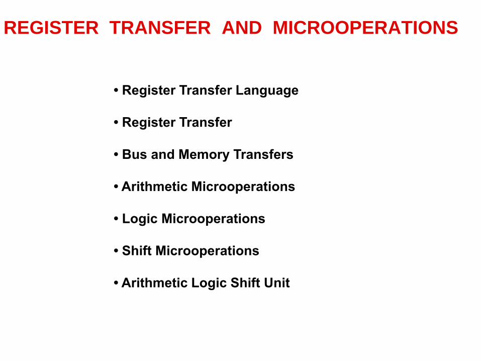
REGISTER TRANSFER AND MICROOPERATIONS
• Register Transfer Language
• Register Transfer
• Bus and Memory Transfers
• Arithmetic Microoperations
• Logic Microoperations
• Shift Microoperations
• Arithmetic Logic Shift Unit
SIMPLE DIGITAL SYSTEMS
• Combinational and sequential circuits can be used to create simple digital systems.
• These are the low-level building blocks of a digital computer.
• Simple digital systems are frequently characterized in terms of
– the registers they contain, and
– the operations that they perform.
• Typically,
– What operations are performed on the data in the registers
– What information is passed between registers
MICROOPERATIONS (1)
Register Transfer Language
• The operations on the data in registers are called microoperations.
• The functions built into registers are examples of microoperations
– Shift
– Load
– Clear
– Increment
– …
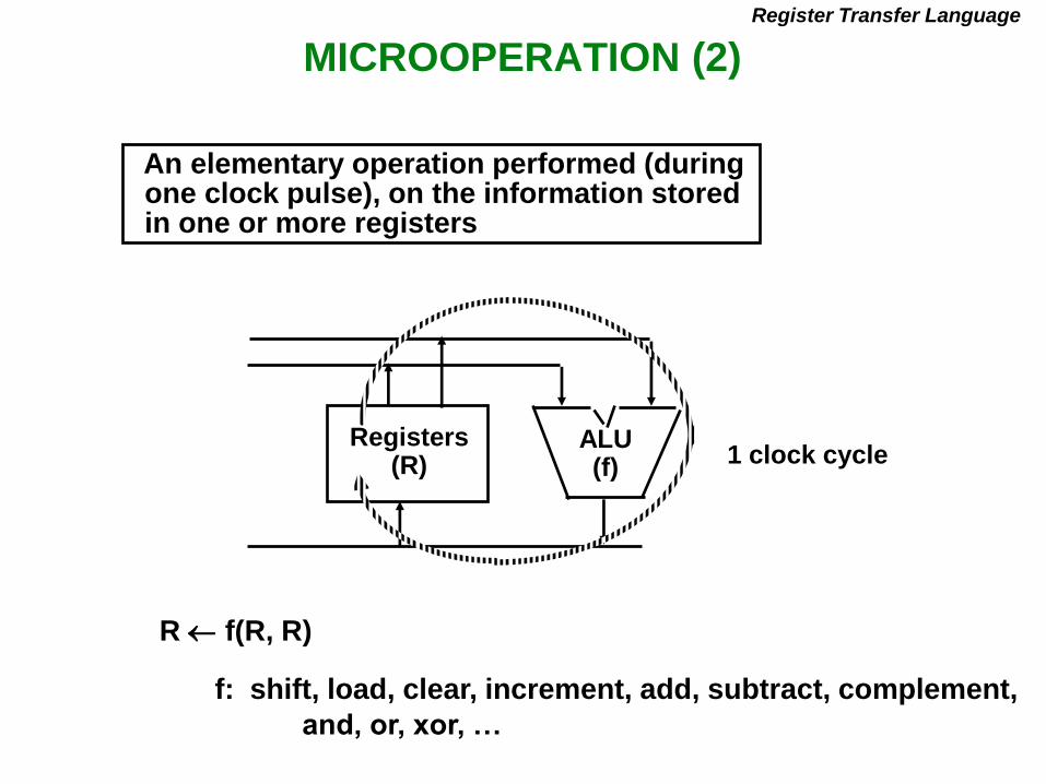
MICROOPERATION (2)
An elementary operation performed (during one clock pulse), on the information stored in one or more registers
R f(R, R)
f: shift, load, clear, increment, add, subtract, complement,
and, or, xor, …
ALU(f)
Registers(R) 1 clock cycle
Register Transfer Language
ORGANIZATION OF A DIGITAL SYSTEM
- Set of registers and their functions
- Microoperations set
Set of allowable microoperations providedby the organization of the computer
- Control signals that initiate the sequence of microoperations (to perform the functions)
• Definition of the (internal) organization of a computer
Register Transfer Language
REGISTER TRANSFER LEVEL
Register Transfer Language
• Viewing a computer, or any digital system, in this way is called the register transfer level
• This is because we’re focusing on
– The system’s registers
– The data transformations in them, and
– The data transfers between them.
REGISTER TRANSFER LANGUAGE
Register Transfer Language
• Rather than specifying a digital system in words, a specific notation is used, register transfer language
• For any function of the computer, the register transfer language can be used to describe the (sequence of) microoperations
• Register transfer language
– A symbolic language
– A convenient tool for describing the internal organization of digital computers
– Can also be used to facilitate the design process of digital systems.
DESIGNATION OF REGISTERS
Register Transfer Language
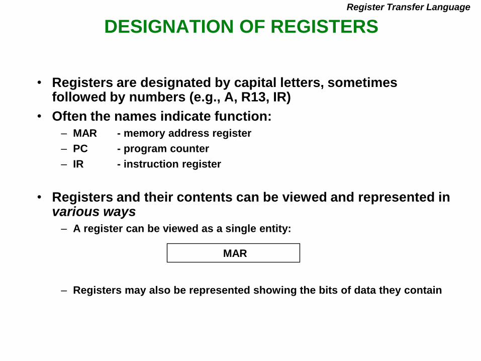
• Registers are designated by capital letters, sometimes followed by numbers (e.g., A, R13, IR)
• Often the names indicate function:
– MAR - memory address register
– PC - program counter
– IR - instruction register
• Registers and their contents can be viewed and represented in various ways
– A register can be viewed as a single entity:
– Registers may also be represented showing the bits of data they contain
MAR
DESIGNATION OF REGISTERS
Register Transfer Language
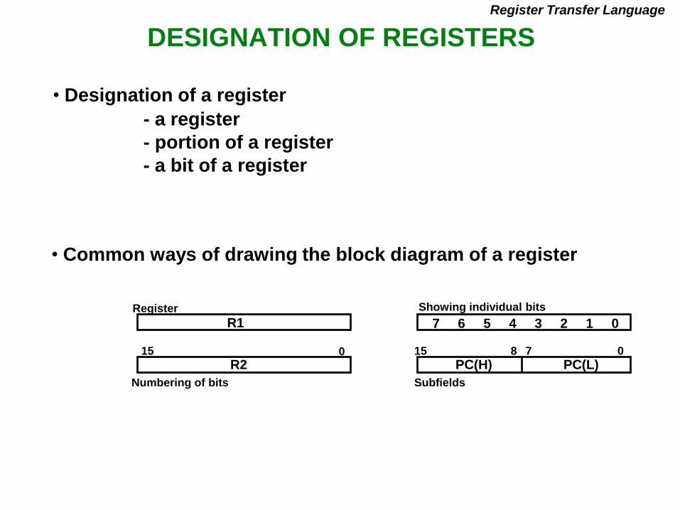
R1Register
Numbering of bits
Showing individual bits
Subfields
PC(H) PC(L)15 8 7 0
- a register
- portion of a register
- a bit of a register
• Common ways of drawing the block diagram of a register
7 6 5 4 3 2 1 0
R215 0
• Designation of a register
REGISTER TRANSFER
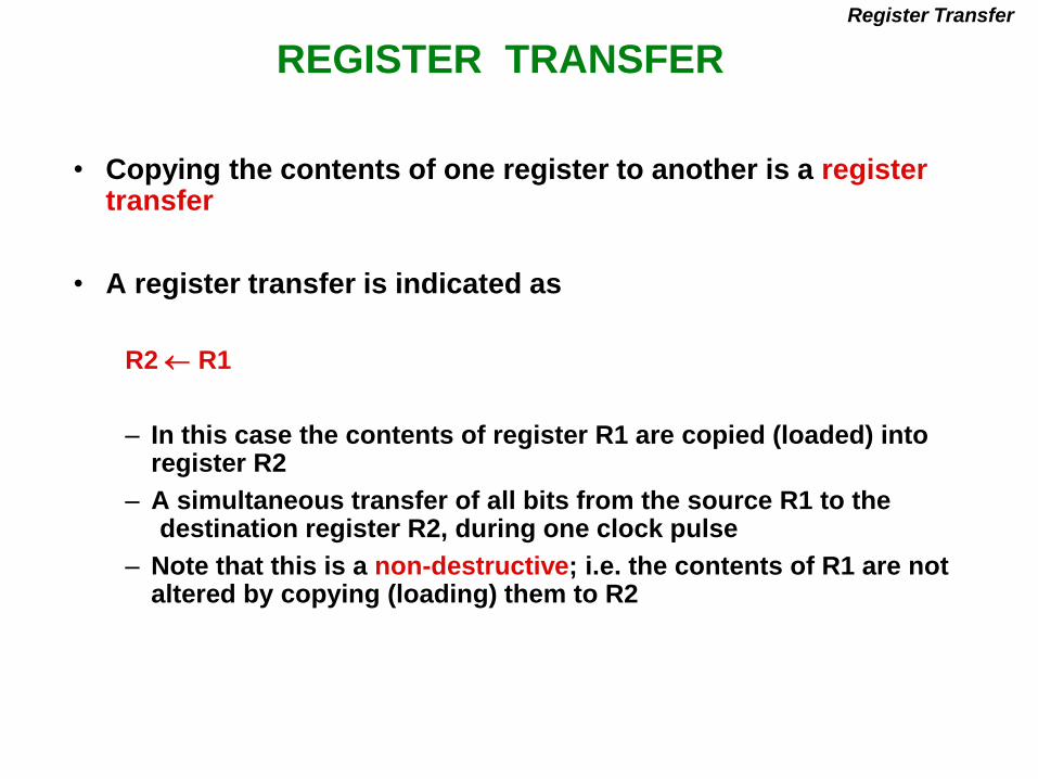
Register Transfer
• Copying the contents of one register to another is a register transfer
• A register transfer is indicated as
R2 R1
– In this case the contents of register R1 are copied (loaded) into register R2
– A simultaneous transfer of all bits from the source R1 to the destination register R2, during one clock pulse
– Note that this is a non-destructive; i.e. the contents of R1 are not altered by copying (loading) them to R2
REGISTER TRANSFER
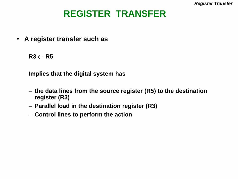
Register Transfer
• A register transfer such as
R3 R5
Implies that the digital system has
– the data lines from the source register (R5) to the destination register (R3)
– Parallel load in the destination register (R3)
– Control lines to perform the action
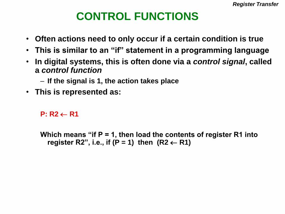
CONTROL FUNCTIONS
Register Transfer
• Often actions need to only occur if a certain condition is true
• This is similar to an “if” statement in a programming language
• In digital systems, this is often done via a control signal, called a control function
– If the signal is 1, the action takes place
• This is represented as:
P: R2 R1
Which means “if P = 1, then load the contents of register R1 into register R2”, i.e., if (P = 1) then (R2 R1)
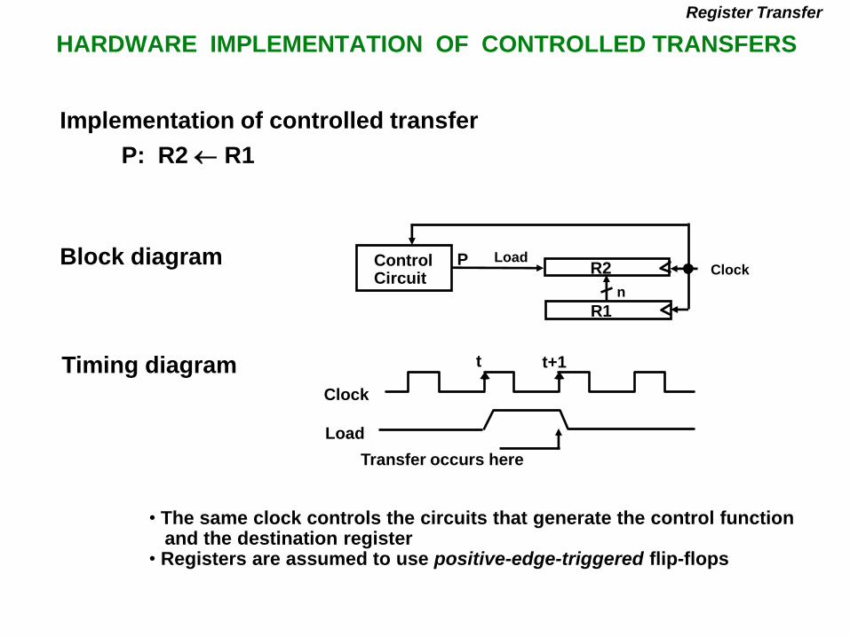
HARDWARE IMPLEMENTATION OF CONTROLLED TRANSFERS
Implementation of controlled transfer
P: R2 R1
Block diagram
Timing diagram
Clock
Register Transfer
Transfer occurs here
R2
R1
Control Circuit
LoadP
n
Clock
Load
t t+1
• The same clock controls the circuits that generate the control functionand the destination register
• Registers are assumed to use positive-edge-triggered flip-flops
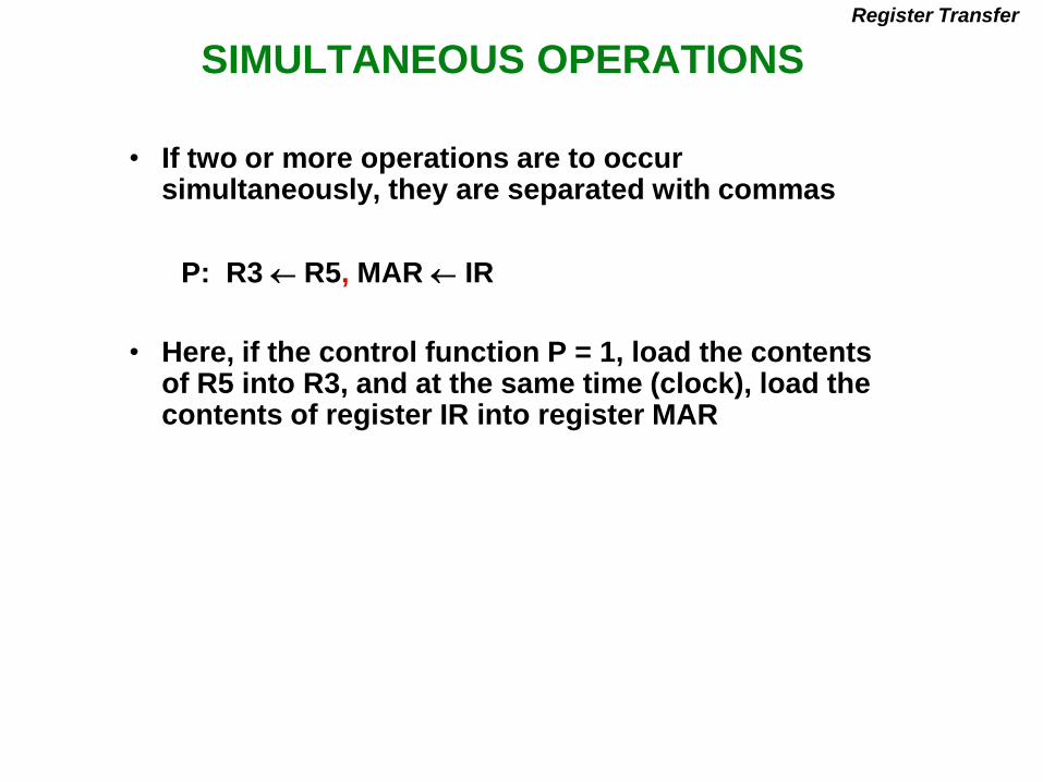
SIMULTANEOUS OPERATIONS
Register Transfer
• If two or more operations are to occur simultaneously, they are separated with commas
P: R3 R5, MAR IR
• Here, if the control function P = 1, load the contents of R5 into R3, and at the same time (clock), load the contents of register IR into register MAR
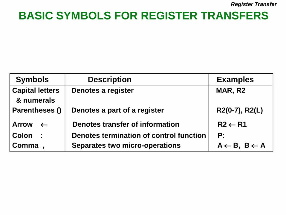
BASIC SYMBOLS FOR REGISTER TRANSFERS
Capital letters Denotes a register MAR, R2
& numerals
Parentheses () Denotes a part of a register R2(0-7), R2(L)
Arrow Denotes transfer of information R2 R1
Colon : Denotes termination of control function P:
Comma , Separates two micro-operations A B, B A
Symbols Description Examples
Register Transfer
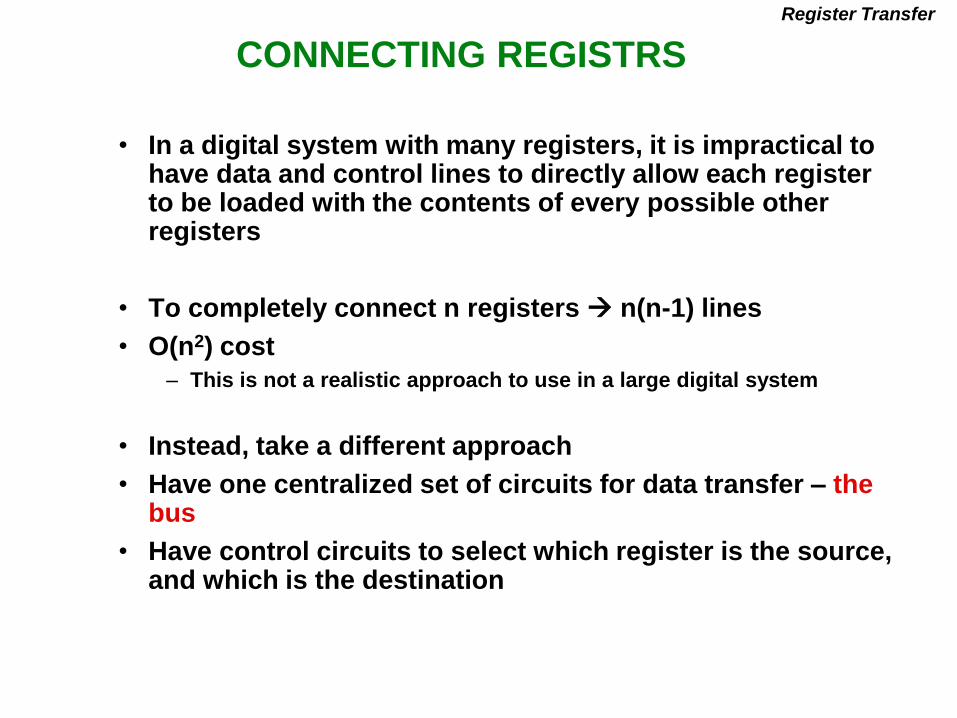
CONNECTING REGISTRS
Register Transfer
• In a digital system with many registers, it is impractical to have data and control lines to directly allow each register to be loaded with the contents of every possible other registers
• To completely connect n registers n(n-1) lines
• O(n2) cost
– This is not a realistic approach to use in a large digital system
• Instead, take a different approach
• Have one centralized set of circuits for data transfer – the bus
• Have control circuits to select which register is the source, and which is the destination
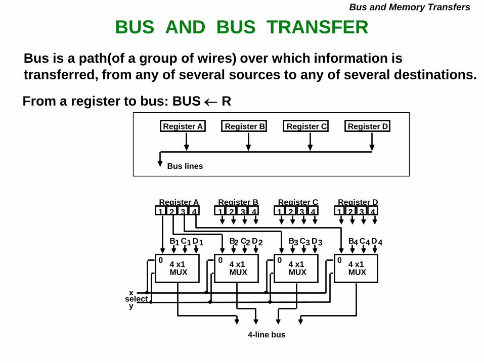
BUS AND BUS TRANSFER
Bus is a path(of a group of wires) over which information is
transferred, from any of several sources to any of several destinations.
From a register to bus: BUS R
1 2 3 4 1 2 3 4 1 2 3 4 1 2 3 4
Register A Register B Register C Register D
B C D1 1 1
4 x1MUX
B C D2 2 2
4 x1MUX
B C D3 3 3
4 x1MUX
B C D4 4 4
4 x1MUX
4-line bus
x
yselect
0 0 0 0
Register A Register B Register C Register D
Bus lines
Bus and Memory Transfers
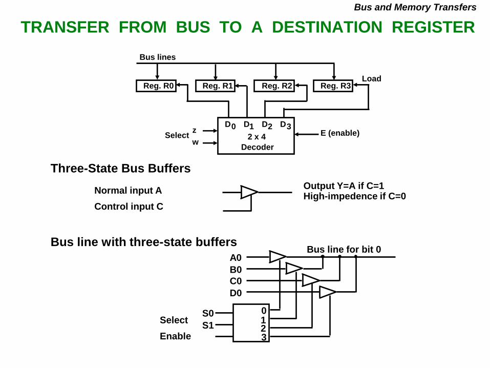
TRANSFER FROM BUS TO A DESTINATION REGISTER
Three-State Bus Buffers
Bus line with three-state buffers
Reg. R0 Reg. R1 Reg. R2 Reg. R3
Bus lines
2 x 4
Decoder
Load
D0 D1 D2 D3z
wSelect E (enable)
Output Y=A if C=1High-impedence if C=0
Normal input A
Control input C
Select
Enable
0123
S0
S1
A0
B0
C0
D0
Bus line for bit 0
Bus and Memory Transfers
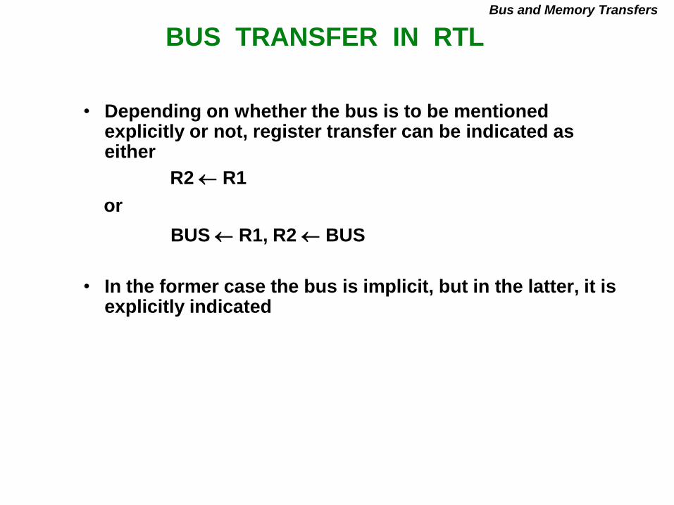
BUS TRANSFER IN RTL
Bus and Memory Transfers
• Depending on whether the bus is to be mentioned explicitly or not, register transfer can be indicated as either
or
• In the former case the bus is implicit, but in the latter, it is explicitly indicated
R2 R1
BUS R1, R2 BUS
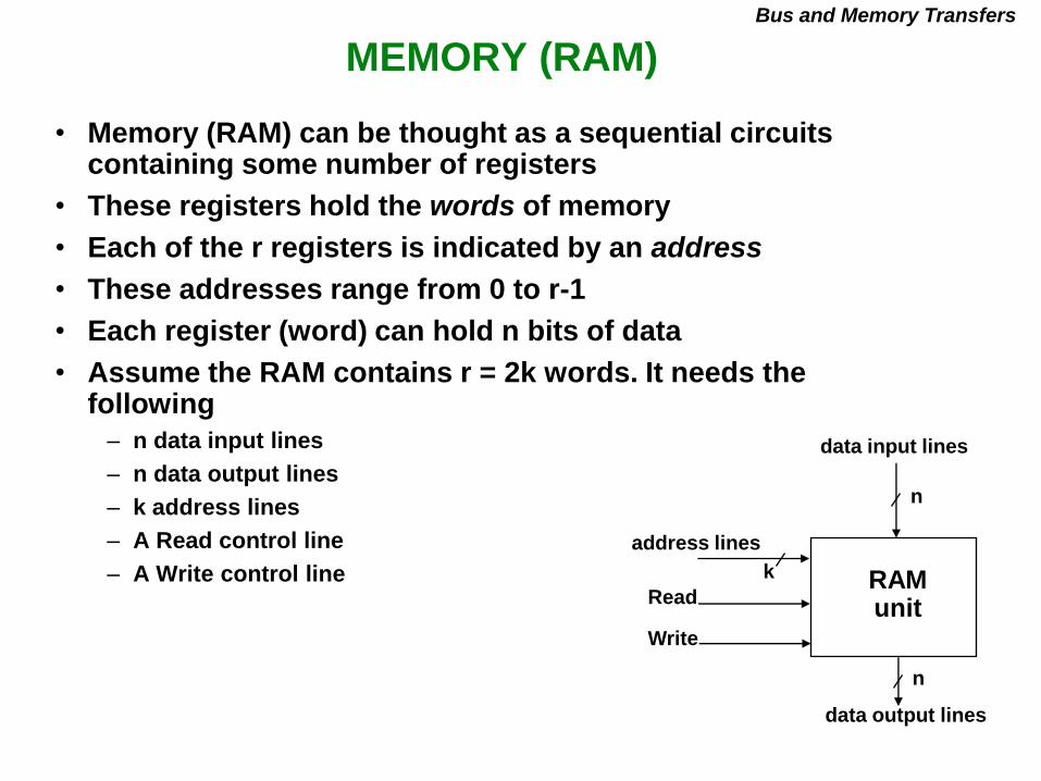
MEMORY (RAM)
Bus and Memory Transfers
• Memory (RAM) can be thought as a sequential circuits containing some number of registers
• These registers hold the words of memory
• Each of the r registers is indicated by an address
• These addresses range from 0 to r-1
• Each register (word) can hold n bits of data
• Assume the RAM contains r = 2k words. It needs the following
– n data input lines
– n data output lines
– k address lines
– A Read control line
– A Write control line
data input lines
data output lines
n
n
k
address lines
Read
Write
RAMunit
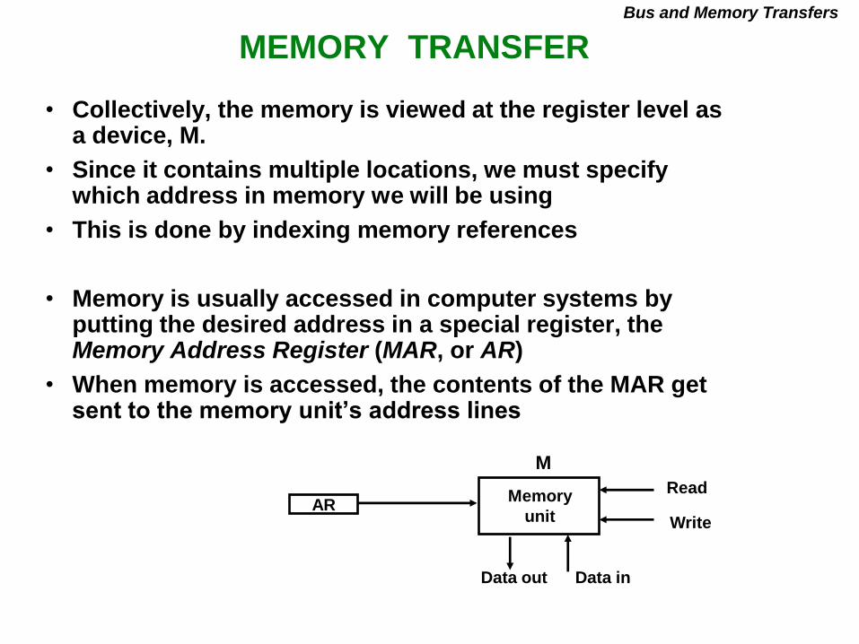
MEMORY TRANSFER
Bus and Memory Transfers
• Collectively, the memory is viewed at the register level as a device, M.
• Since it contains multiple locations, we must specify which address in memory we will be using
• This is done by indexing memory references
• Memory is usually accessed in computer systems by putting the desired address in a special register, the Memory Address Register (MAR, or AR)
• When memory is accessed, the contents of the MAR get sent to the memory unit’s address lines
ARMemory
unit
Read
Write
Data inData out
M
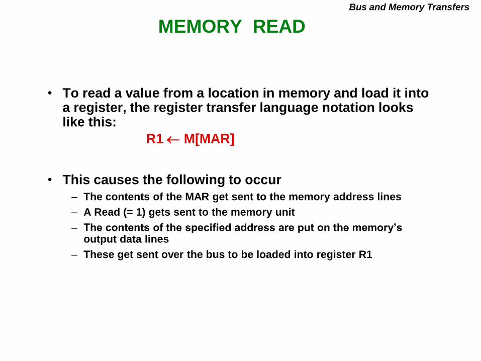
MEMORY READ
Bus and Memory Transfers
• To read a value from a location in memory and load it into a register, the register transfer language notation looks like this:
• This causes the following to occur
– The contents of the MAR get sent to the memory address lines
– A Read (= 1) gets sent to the memory unit
– The contents of the specified address are put on the memory’s output data lines
– These get sent over the bus to be loaded into register R1
R1 M[MAR]
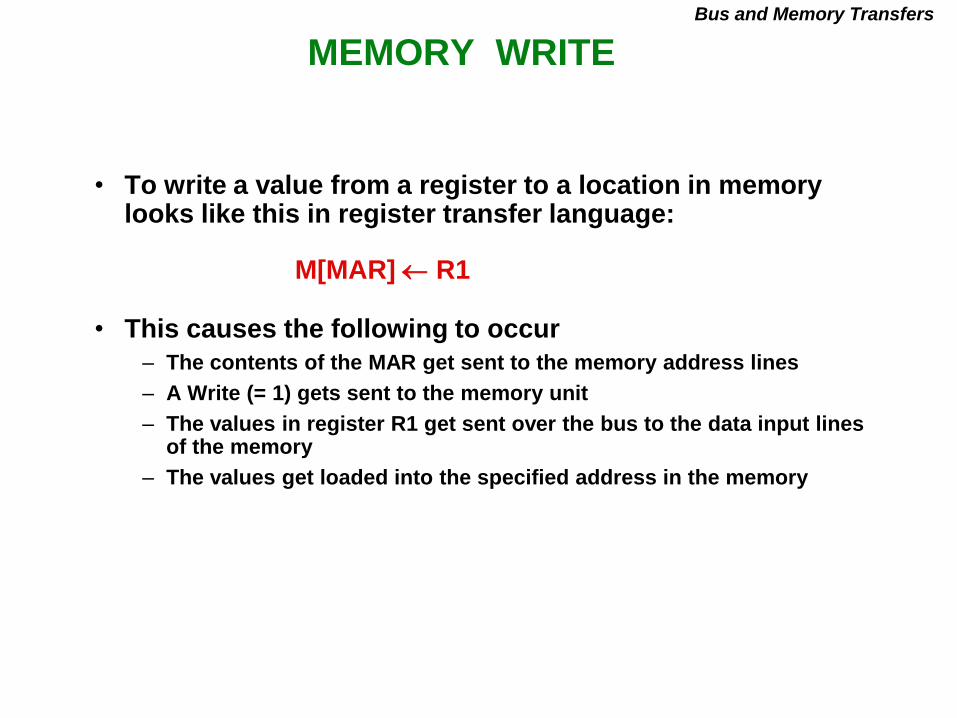
MEMORY WRITE
Bus and Memory Transfers
• To write a value from a register to a location in memory looks like this in register transfer language:
• This causes the following to occur
– The contents of the MAR get sent to the memory address lines
– A Write (= 1) gets sent to the memory unit
– The values in register R1 get sent over the bus to the data input lines of the memory
– The values get loaded into the specified address in the memory
M[MAR] R1

SUMMARY OF R. TRANSFER MICROOPERATIONS
Bus and Memory Transfers
A B Transfer content of reg. B into reg. A
AR DR(AD) Transfer content of AD portion of reg. DR into reg. AR
A constant Transfer a binary constant into reg. A
ABUS R1, Transfer content of R1 into bus A and, at the same time,
R2 ABUS transfer content of bus A into R2
AR Address register
DR Data register
M[R] Memory word specified by reg. R
M Equivalent to M[AR]
DR M Memory read operation: transfers content of
memory word specified by AR into DR
M DR Memory write operation: transfers content of
DR into memory word specified by AR
MICROOPERATIONS
• Computer system microoperations are of four types:
- Register transfer microoperations
- Arithmetic microoperations
- Logic microoperations
- Shift microoperations
Arithmetic Microoperations
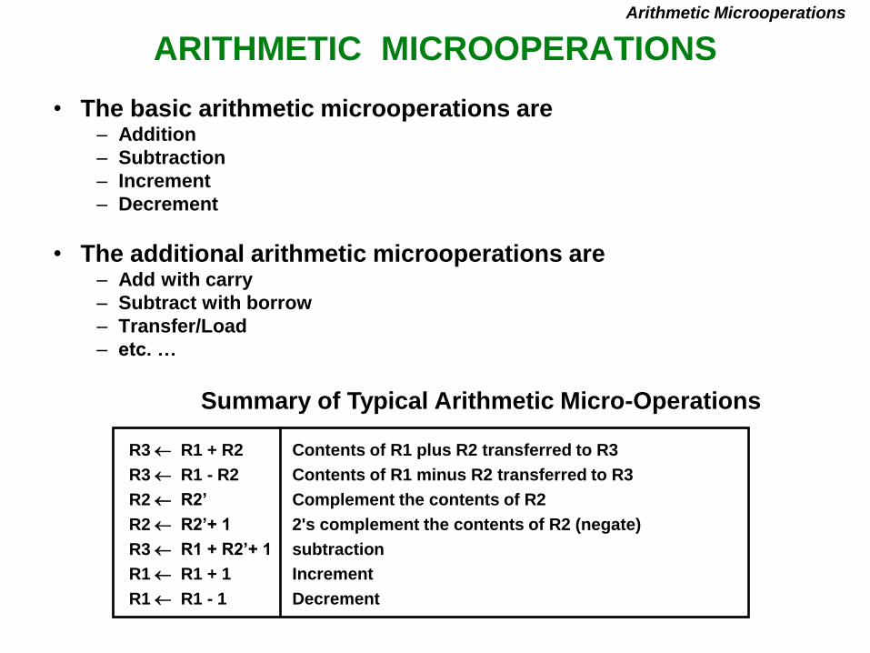
ARITHMETIC MICROOPERATIONS
Summary of Typical Arithmetic Micro-Operations
Arithmetic Microoperations
R3 R1 + R2 Contents of R1 plus R2 transferred to R3
R3 R1 - R2 Contents of R1 minus R2 transferred to R3
R2 R2’ Complement the contents of R2
R2 R2’+ 1 2's complement the contents of R2 (negate)
R3 R1 + R2’+ 1 subtraction
R1 R1 + 1 Increment
R1 R1 - 1 Decrement
• The basic arithmetic microoperations are– Addition
– Subtraction
– Increment
– Decrement
• The additional arithmetic microoperations are– Add with carry
– Subtract with borrow
– Transfer/Load
– etc. …
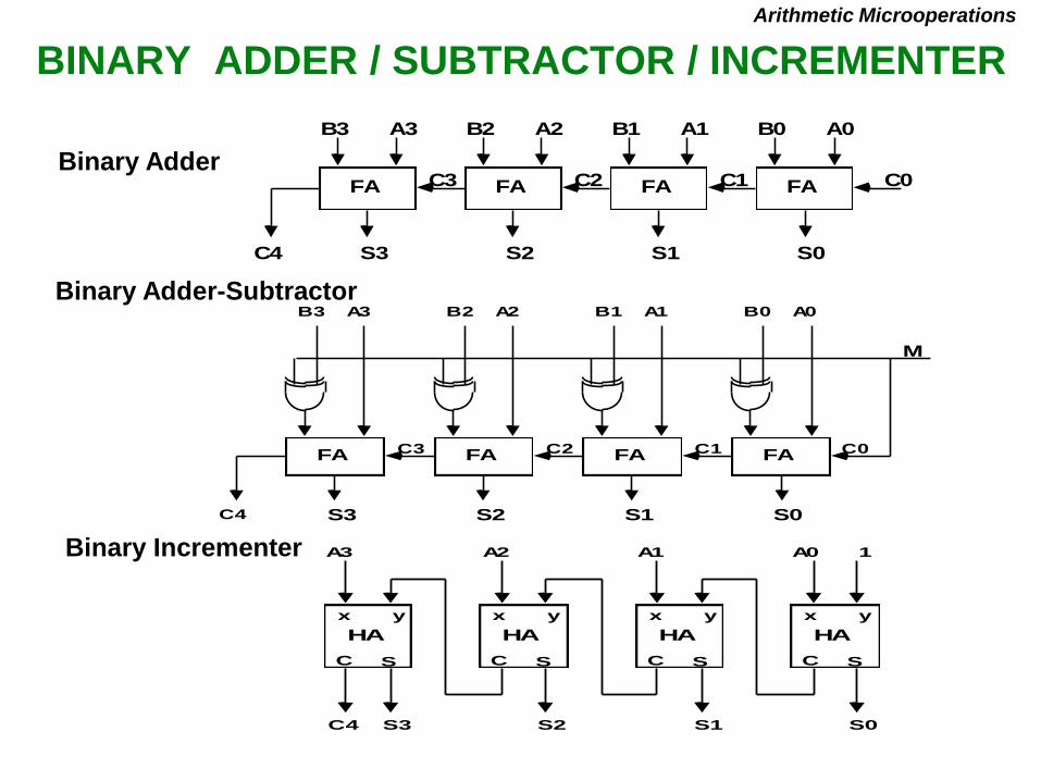
BINARY ADDER / SUBTRACTOR / INCREMENTER
FA
B0 A0
S0
C0FA
B1 A1
S1
C1FA
B2 A2
S2
C2FA
B3 A3
S3
C3
C4
Binary Adder-Subtractor
FA
B0 A0
S0
C0C1FA
B1 A1
S1
C2FA
B2 A2
S2
C3FA
B3 A3
S3C4
M
Binary Incrementer
HA
x y
C S
A0 1
S0
HA
x y
C S
A1
S1
HA
x y
C S
A2
S2
HA
x y
C S
A3
S3C4
Binary Adder
Arithmetic Microoperations
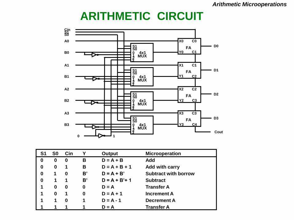
ARITHMETIC CIRCUIT
S1S00123
4x1MUX
X0
Y0
C0
C1
D0FA
S1S00123
4x1MUX
X1
Y1
C1
C2
D1FA
S1S00123
4x1MUX
X2
Y2
C2
C3
D2FA
S1S00123
4x1MUX
X3
Y3
C3
C4
D3FA
Cout
A0
B0
A1
B1
A2
B2
A3
B3
0 1
S0S1Cin
S1 S0 Cin Y Output Microoperation
0 0 0 B D = A + B Add
0 0 1 B D = A + B + 1 Add with carry
0 1 0 B’ D = A + B’ Subtract with borrow
0 1 1 B’ D = A + B’+ 1 Subtract
1 0 0 0 D = A Transfer A
1 0 1 0 D = A + 1 Increment A
1 1 0 1 D = A - 1 Decrement A
1 1 1 1 D = A Transfer A
Arithmetic Microoperations
LOGIC MICROOPERATIONS
Logic Microoperations
• Specify binary operations on the strings of bits in registers
– Logic microoperations are bit-wise operations, i.e., they work on the individual bits of data
– useful for bit manipulations on binary data
– useful for making logical decisions based on the bit value
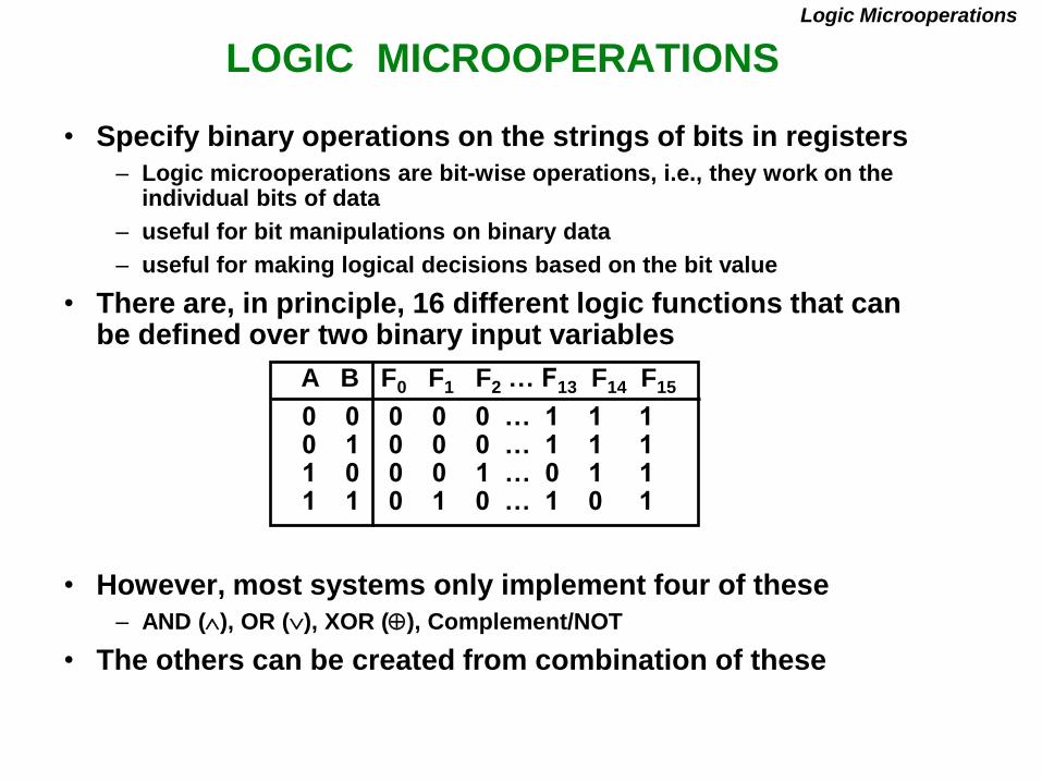
• There are, in principle, 16 different logic functions that can be defined over two binary input variables
• However, most systems only implement four of these
– AND (), OR (), XOR (), Complement/NOT
• The others can be created from combination of these
0 0 0 0 0 … 1 1 10 1 0 0 0 … 1 1 11 0 0 0 1 … 0 1 11 1 0 1 0 … 1 0 1
A B F0 F1 F2 … F13 F14 F15
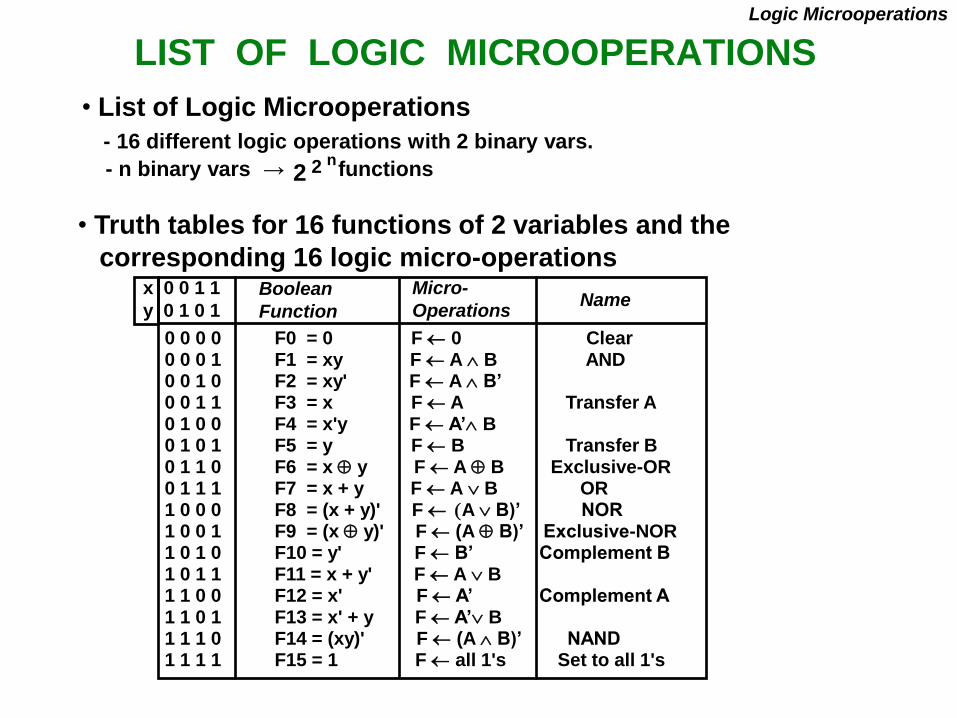
LIST OF LOGIC MICROOPERATIONS
• List of Logic Microoperations
- 16 different logic operations with 2 binary vars.
- n binary vars → functions2 2 n
• Truth tables for 16 functions of 2 variables and the
corresponding 16 logic micro-operationsBoolean
Function
Micro-
OperationsName
x 0 0 1 1
y 0 1 0 1
Logic Microoperations
0 0 0 0 F0 = 0 F 0 Clear0 0 0 1 F1 = xy F A B AND0 0 1 0 F2 = xy' F A B’0 0 1 1 F3 = x F A Transfer A0 1 0 0 F4 = x'y F A’ B0 1 0 1 F5 = y F B Transfer B0 1 1 0 F6 = x y F A B Exclusive-OR0 1 1 1 F7 = x + y F A B OR1 0 0 0 F8 = (x + y)' F A B)’ NOR1 0 0 1 F9 = (x y)' F (A B)’ Exclusive-NOR1 0 1 0 F10 = y' F B’ Complement B1 0 1 1 F11 = x + y' F A B1 1 0 0 F12 = x' F A’ Complement A1 1 0 1 F13 = x' + y F A’ B1 1 1 0 F14 = (xy)' F (A B)’ NAND1 1 1 1 F15 = 1 F all 1's Set to all 1's
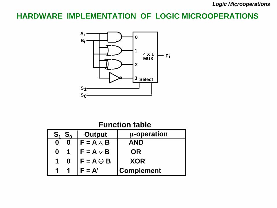
HARDWARE IMPLEMENTATION OF LOGIC MICROOPERATIONS
0 0 F = A B AND
0 1 F = AB OR
1 0 F = A B XOR
1 1 F = A’ Complement
S1 S0 Output -operation
Function table
Logic Microoperations
B
A
S
S
F
1
0
i
i
i0
1
2
3
4 X 1MUX
Select
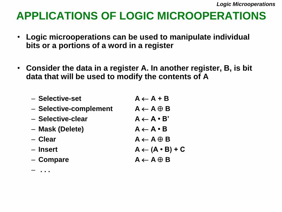
APPLICATIONS OF LOGIC MICROOPERATIONS
Logic Microoperations
• Logic microoperations can be used to manipulate individual bits or a portions of a word in a register
• Consider the data in a register A. In another register, B, is bit data that will be used to modify the contents of A
– Selective-set A A + B
– Selective-complement A A B
– Selective-clear A A • B’
– Mask (Delete) A A • B
– Clear A A B
– Insert A (A • B) + C
– Compare A A B
– . . .

SELECTIVE SET
Logic Microoperations
• In a selective set operation, the bit pattern in B is used to setcertain bits in A
1 1 0 0 At
1 0 1 0 B
1 1 1 0 At+1 (A A + B)
• If a bit in B is set to 1, that same position in A gets set to 1, otherwise that bit in A keeps its previous value
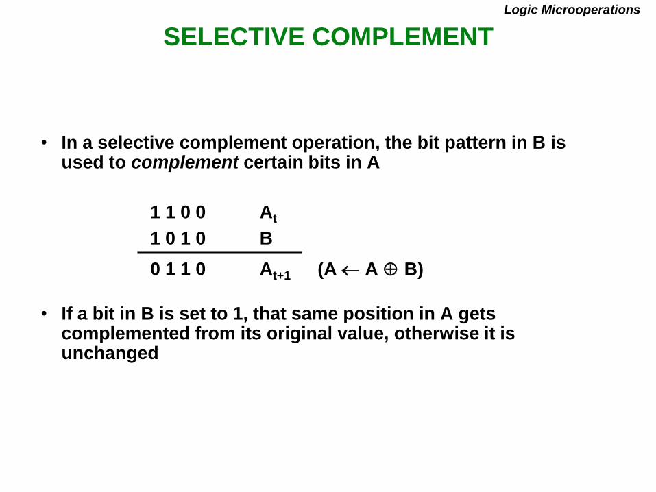
SELECTIVE COMPLEMENT
Logic Microoperations
• In a selective complement operation, the bit pattern in B is used to complement certain bits in A
1 1 0 0 At
1 0 1 0 B
0 1 1 0 At+1 (A A B)
• If a bit in B is set to 1, that same position in A gets complemented from its original value, otherwise it is unchanged
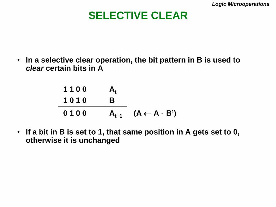
SELECTIVE CLEAR
Logic Microoperations
• In a selective clear operation, the bit pattern in B is used to clear certain bits in A
1 1 0 0 At
1 0 1 0 B
0 1 0 0 At+1 (A A B’)
• If a bit in B is set to 1, that same position in A gets set to 0, otherwise it is unchanged
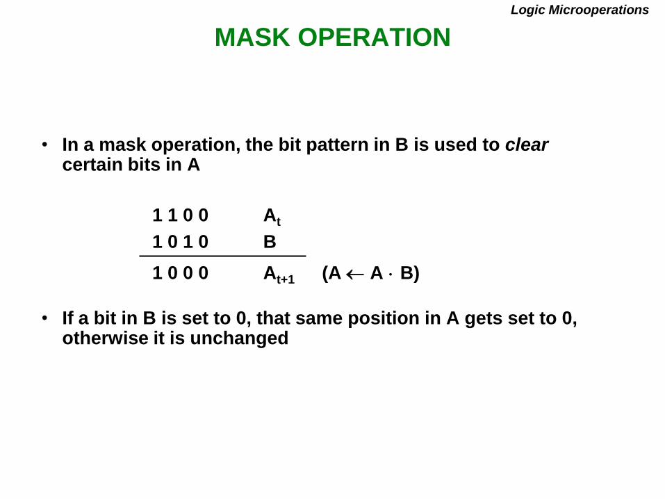
MASK OPERATION
Logic Microoperations
• In a mask operation, the bit pattern in B is used to clearcertain bits in A
1 1 0 0 At
1 0 1 0 B
1 0 0 0 At+1 (A A B)
• If a bit in B is set to 0, that same position in A gets set to 0, otherwise it is unchanged
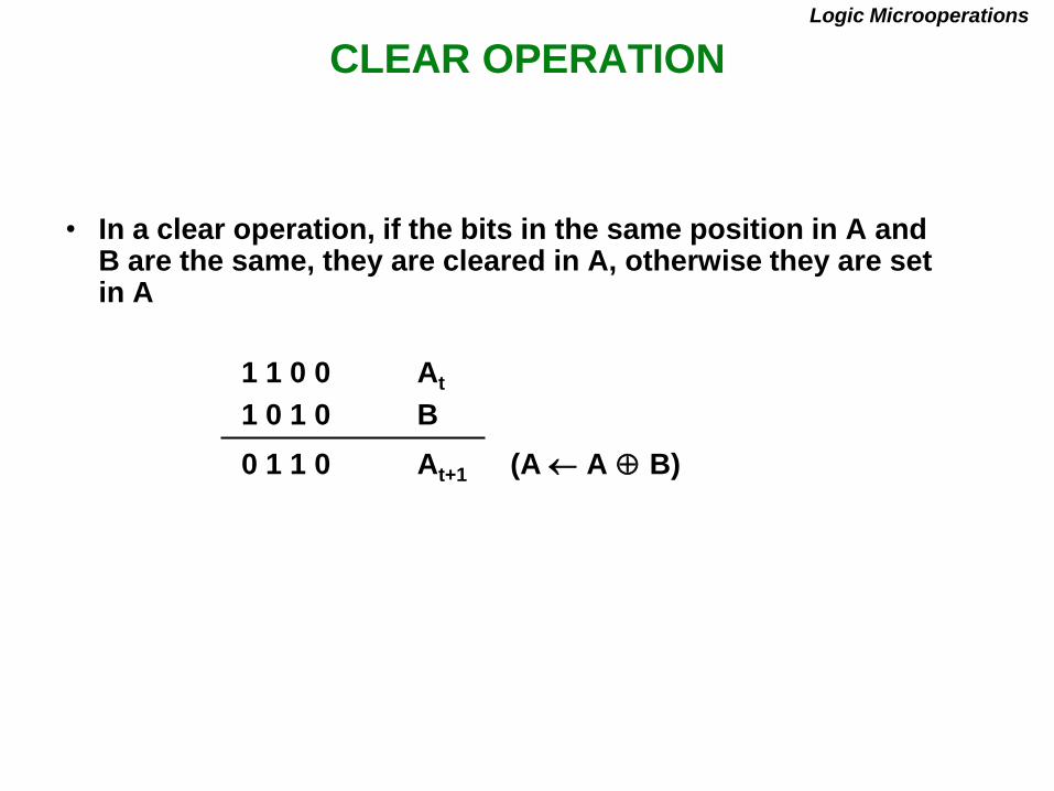
CLEAR OPERATION
Logic Microoperations
• In a clear operation, if the bits in the same position in A and B are the same, they are cleared in A, otherwise they are set in A
1 1 0 0 At
1 0 1 0 B
0 1 1 0 At+1 (A A B)
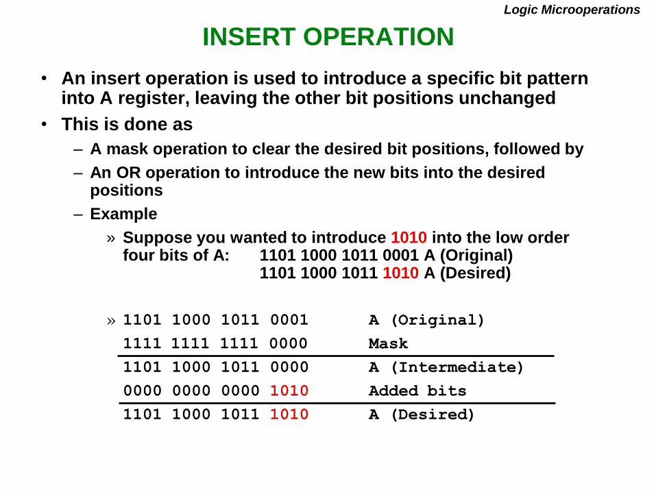
INSERT OPERATION
Logic Microoperations
• An insert operation is used to introduce a specific bit pattern into A register, leaving the other bit positions unchanged
• This is done as
– A mask operation to clear the desired bit positions, followed by
– An OR operation to introduce the new bits into the desired positions
– Example
» Suppose you wanted to introduce 1010 into the low order four bits of A: 1101 1000 1011 0001 A (Original)
1101 1000 1011 1010 A (Desired)
» 1101 1000 1011 0001 A (Original)
1111 1111 1111 0000 Mask
1101 1000 1011 0000 A (Intermediate)
0000 0000 0000 1010 Added bits
1101 1000 1011 1010 A (Desired)
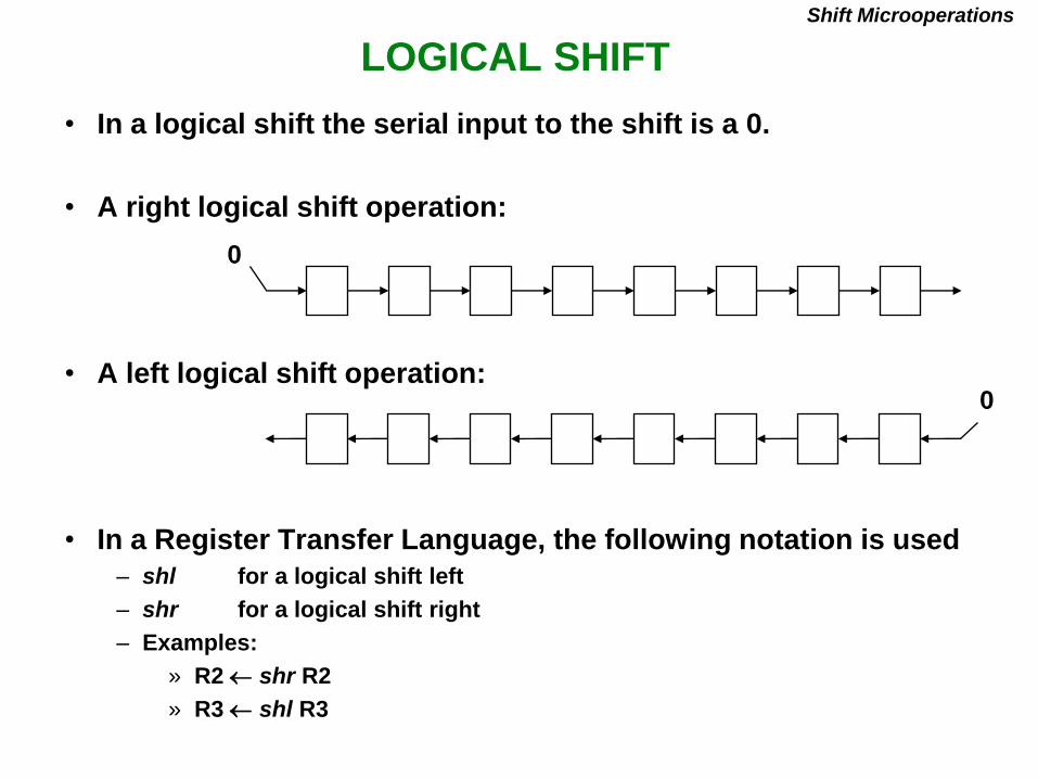
LOGICAL SHIFT
Shift Microoperations
• In a logical shift the serial input to the shift is a 0.
• A right logical shift operation:
• A left logical shift operation:
• In a Register Transfer Language, the following notation is used
– shl for a logical shift left
– shr for a logical shift right
– Examples:
» R2 shr R2
» R3 shl R3
0
0
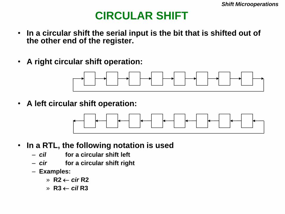
CIRCULAR SHIFT
Shift Microoperations
• In a circular shift the serial input is the bit that is shifted out of the other end of the register.
• A right circular shift operation:
• A left circular shift operation:
• In a RTL, the following notation is used– cil for a circular shift left
– cir for a circular shift right
– Examples:
» R2 cir R2
» R3 cil R3
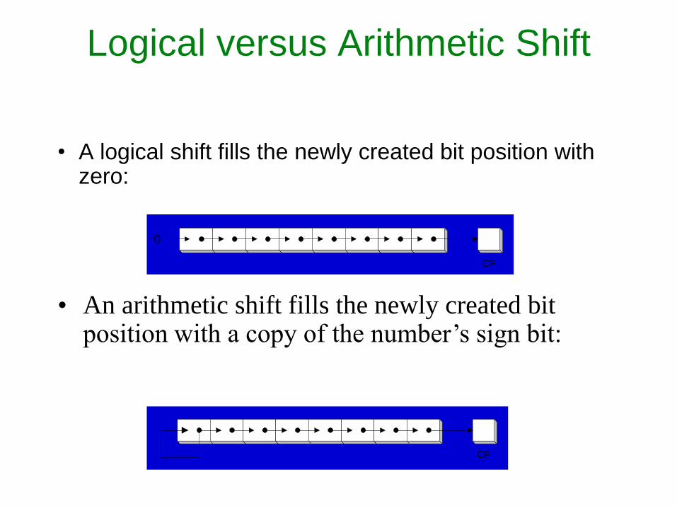
Logical versus Arithmetic Shift
• A logical shift fills the newly created bit position with zero:
• An arithmetic shift fills the newly created bit position with a copy of the number’s sign bit:
CF
0
CF
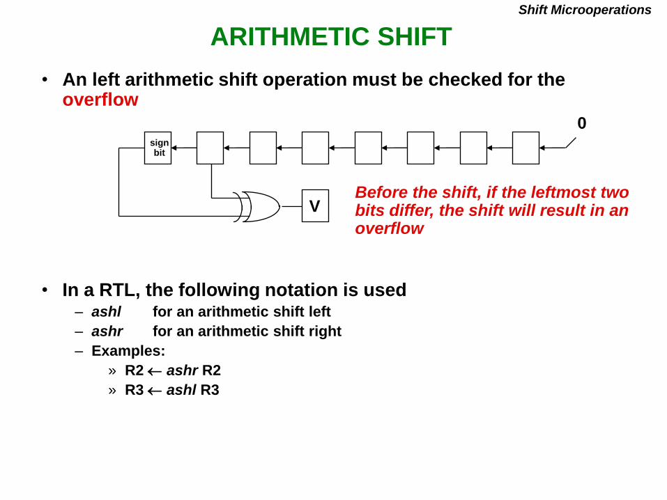
ARITHMETIC SHIFT
Shift Microoperations
• An left arithmetic shift operation must be checked for the overflow
0
VBefore the shift, if the leftmost twobits differ, the shift will result in anoverflow
• In a RTL, the following notation is used– ashl for an arithmetic shift left
– ashr for an arithmetic shift right
– Examples:
» R2 ashr R2
» R3 ashl R3
signbit
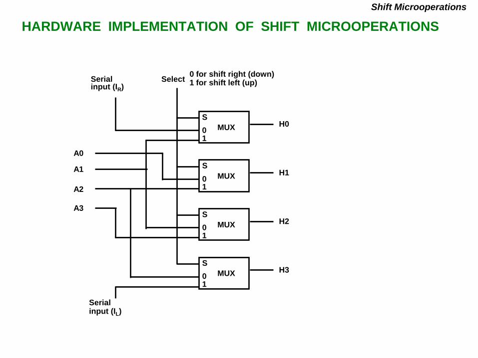
HARDWARE IMPLEMENTATION OF SHIFT MICROOPERATIONS
Shift Microoperations
S
01
H0MUX
S
01
H1MUX
S
01
H2MUX
S
01
H3MUX
Select0 for shift right (down) 1 for shift left (up)Serial
input (IR)
A0
A1
A2
A3
Serialinput (IL)
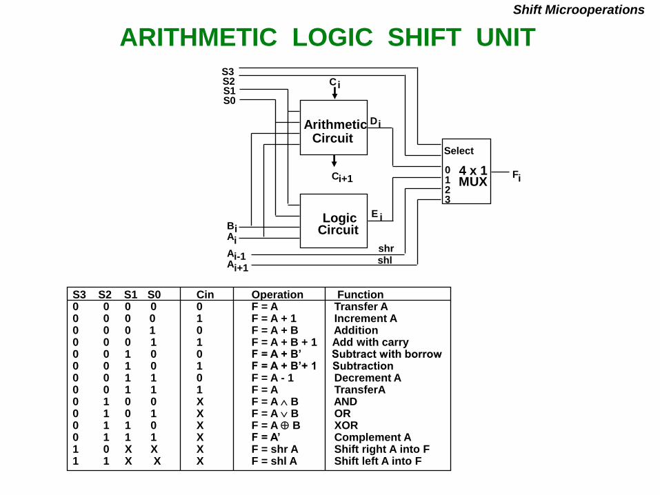
ARITHMETIC LOGIC SHIFT UNIT
S3 S2 S1 S0 Cin Operation Function0 0 0 0 0 F = A Transfer A0 0 0 0 1 F = A + 1 Increment A0 0 0 1 0 F = A + B Addition0 0 0 1 1 F = A + B + 1 Add with carry0 0 1 0 0 F = A + B’ Subtract with borrow0 0 1 0 1 F = A + B’+ 1 Subtraction0 0 1 1 0 F = A - 1 Decrement A0 0 1 1 1 F = A TransferA0 1 0 0 X F = A B AND0 1 0 1 X F = A B OR0 1 1 0 X F = A B XOR0 1 1 1 X F = A’ Complement A1 0 X X X F = shr A Shift right A into F1 1 X X X F = shl A Shift left A into F
Shift Microoperations
ArithmeticCircuit
LogicCircuit
C
C 4 x 1MUX
Select
0123
F
S3S2S1S0
BA
i
A
D
A
E
shrshl
i+1 i
ii
i+1i-1
i
i
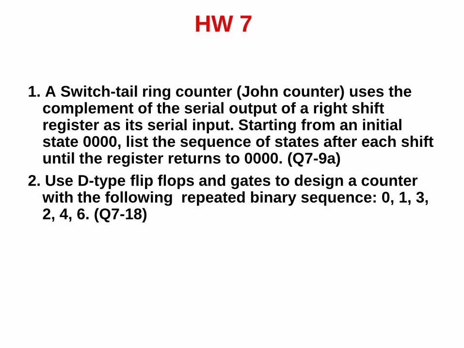
HW 7
1. A Switch-tail ring counter (John counter) uses the complement of the serial output of a right shift register as its serial input. Starting from an initial state 0000, list the sequence of states after each shift until the register returns to 0000. (Q7-9a)
2. Use D-type flip flops and gates to design a counter with the following repeated binary sequence: 0, 1, 3, 2, 4, 6. (Q7-18)