Embed Size (px)
Citation preview
Relation Between Incremental Intrinsic Capacitances and Transconductances in MOS Transistors
Abstract-The ratio of intrinsic substrate and gate capacitances is related to the ratio of substrate transconductance to gate transconduc- tance for a long-channel MOS transistor in strong inversion. It is shown that under certain assumptions the two ratios are approximately equal.
I INTRODUCTION
NCREMENTAL MODELS for the MOS transistor have been provided by several authors. A detailed derivation of such
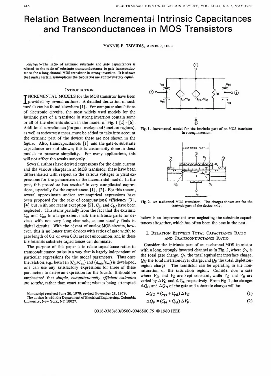
models can be found elsewhere [ l ] . For computer simulations of electronic circuits, the most widely used models for the intrinsic part of a transistor in strong inversion contain some or all of the elements shown in the model of Fig. 1 [2] - [ 6 ] . Additional capacitances (for gate-overlap and junction regions), as well as series resistances, must be added to take into account the extrinsic part of the device; these are not shown in the figure. Also, transcapacitances [ l ] and the gate-to-substrate capacitance are not shown; this is customarily done in these models to preserve simplicity. For many applications, this will not affect the results seriously.
Several authors have derived expressions for the drain current and the various charges in an MOS transistor; these have been differentiated with respect to the various voltages to yield ex- pressions for the parameters of the incremental model. In the past, this procedure has resulted in very complicated expres- sions, especially for the capacitances [ l ] , [2] . For this reason, several approximate and/or semiempirical expressions have been proposed for the sake of computational efficiency [3], [4] but, with one recent exception [5], cbs and Cbd have been neglected. This stems partially from the fact that the extrinsic c b , and cbd to a large extent mask the intrinsic parts for de- vices with not very long channels, as one usually finds in digital circuits. With the advent of analog MOS circuits, how- ever, this is no longer true; devices with ratios of gate width to gate length of 0.1 or even 0.01 are not uncommon, and in these the intrinsic substrate capacitances can dominate.
The purpose of this paper is to relate capacitance ratios to transconductance ratios in a way that is largely independent of particular expressions for the model parameters. Thus once the relation, e.g., between ( c b s / c g s ) and (gmb/gm) is developed, one can use any satisfactory expressions for three of these parameters to derive an expression for the fourth. It should be emphasized that simple, computationally ejpcient estimates are sought, rather than exact results; what is being attempted
Manuscript received June 20,1979;revised November 28,1979. The author is with the Department of Electrical Engineering, Columbia
University, New York, NY 10027.
8 Fig. 1. Incremental model for the intrinsic part of an MOS transistor
in strong inversion.
I I hIh lTRlNSlC PART-: I
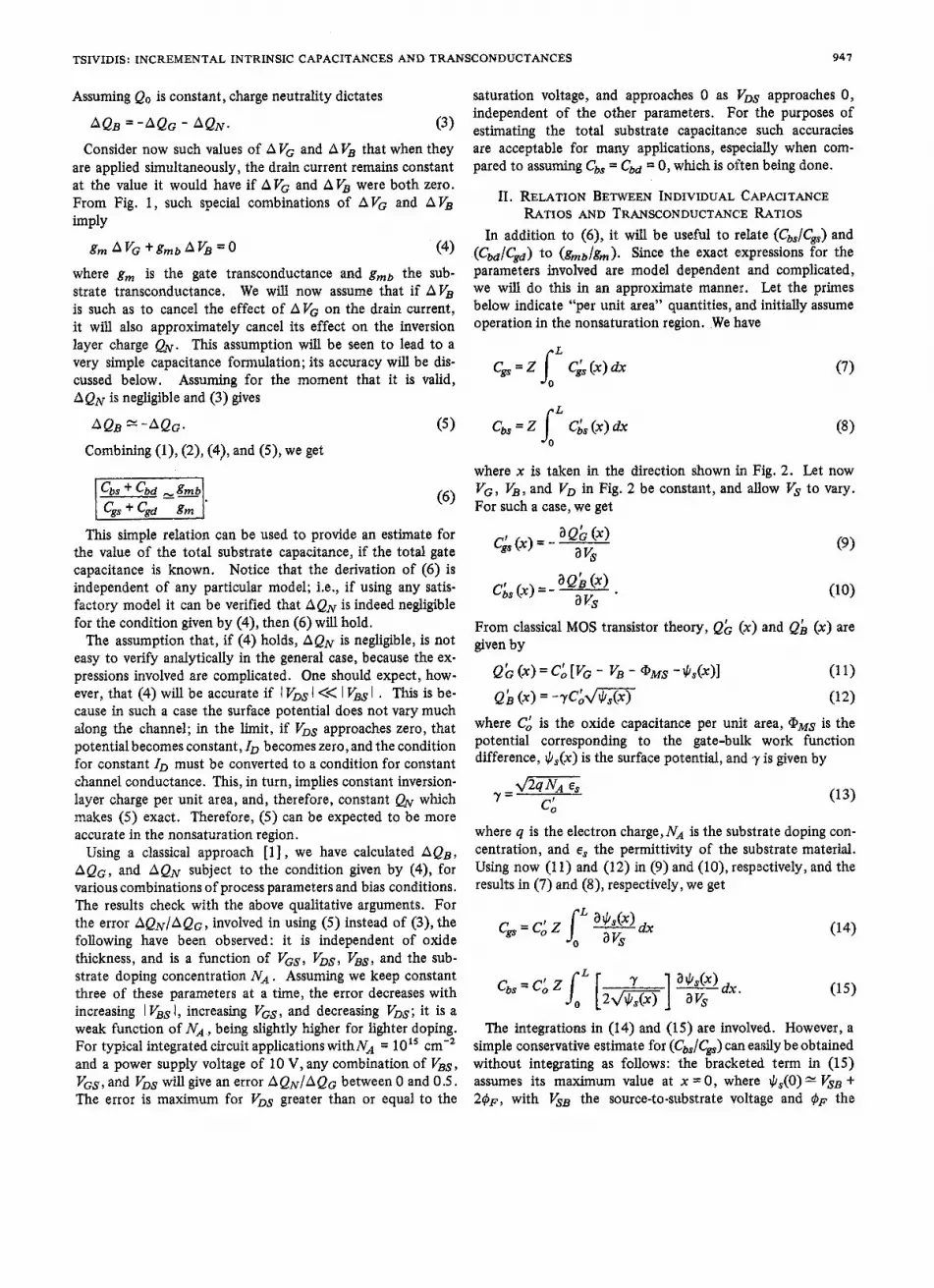
Fig. 2. An n-channel MOS t1:ansistor. The charges shown are for the intrinsic part of the device only.
below is an improvement over neglecting the substrate capaci- tances altogether, which has often been the case in the past.
I. RELATION BETWEEN TOTAL CAPACITANCE RATIO AND TRANSCONDUCTANCE RATIO
Consider the intrinsic part of an n-channel MOS tlransistor with a long, strongly inverted channel as in Fig. 2, where QG is the total gate charge, Qo the total equivalent interface charge, QN the total inversion-layer charge, and QB the total depletion- region charge. The transistor can be operating in the non- saturation or the satura.tion region. Consider now a case where V, and Vs are k:ept constant, while VG and V’ are varied by A VG and A V,, respectively. From Fig. 1, the changes AQc and AQB of the gate and substrate charges will be
0018-9383/80/0500-0946$00.75 0 1980 IEEE
TSIVIDIS: INCREMENTAL INTRINSIC CAPACITANCES AND TRANSCONDUCTANCES 94 7
Assuming Qo is constant, charge neutrality dictates
AQB = - A Q c - AQN. (3)
Consider now such values of A VG and A VB that when they are applied simultaneously, the drain current remains constant at the value it would have if AVG and AVB were both zero. From Fig. 1 , such special combinations of AV, and A VB imply
gm AvG + g m b AvB = o (4)
where g , is the gate transconductance and gmb the sub- strate transconductance. We will now assume that if AVB is such as to cancel the effect of A VG on the drain current, it will also approximately cancel its effect on the inversion layer charge a. This assumption will be seen to lead to a very simple capacitance formulation; its accuracy will be dis- cussed below. Assuming for the moment that it is valid, A QN is negligible and (3) gives
AQB - A Q G . (5 1 Combining (l), (2), (4), and (9 , we get
This simple relation can be used to provide an estimate for the value of the total substrate capacitance, if the total gate capacitance is known. Notice that the derivation of (6) is independent of any particular model; i.e., if using any satis- factory model it can be verified that AQN is indeed negligible for the condition given by (4), then (6) will hold.
The assumption that, if (4) holds, AQN is negligible, is not easy to verify analytically in the general case, because the ex- pressions involved are complicated. One should expect, how- ever, that (4) will be accurate if I VDS l << l VBs l . This is be- cause in such a case the surface potential does not vary much along the channel; in the limit, if VDs approaches zero, that potential becomes constant, ID becomes zero,and the condition for constant ID must be converted to a condition for constant channel conductance. This, in turn, implies constant inversion- layer charge per unit area, and, therefore, constant QN which makes ( 5 ) exact. Therefore, ( 5 ) can be expected to be more accurate in the nonsaturation region.
Using a classical approach [ l ] , we have calculated AQB, AQG, and AQN subject to the condition given by (4), for various combinations of process parameters and bias conditions. The results check with the above qualitative arguments. For the error AQN/AQG, involved in using ( 5 ) instead of (3), the following have been observed: it is independent of oxide thickness, and is a function of V&, VDS, VBs, and the sub- strate doping concentration NA . Assuming we keep constant three of these parameters at a time, the error decreases with increasing I VBs I , increasing V&, and decreasing VDS; it is a weak function of NA , being slightly higher for lighter doping. For typical integrated circuit applications withNA = 10’’ cm-’ and a power supply voltage of 10 V, any combination of VBs, VGS, and VDS will give an error AQN/AQG between 0 and 0.5. The error is maximum for VDs greater than or equal to the
saturation voltage, and approaches 0 as VDS approaches 0, independent of the other parameters. For the purposes of estimating the total substrate capacitance such accuracies are acceptable for many applications, especially when com- pared to assuming CbS = cbd = 0, which is often being done.
11. RELATION BETWEEN INDIVIDUAL CAPACITANCE RATIOS AND TRANSCONDUCTANCE RATIOS
In addition to (6), it will be useful to relate (cb&gs) and (Cbd/Cgd) to (gmb/gm) . Since the exact expressions for the parameters involved are model dependent and complicated, we will do this in an approximate manner. Let the primes below indicate “per unit area” quantities, and initially assume operation in the nonsaturation region. We have
where x is taken in the direction shown in Fig. 2. Let now VG , VB, and V’ in Fig. 2 be constant, and allow Vs to vary. For such a case, we get
(9)
From classical MOS transistor theory, Q b ( x ) and Qh (x) are given by
Qb (x) CL [VG - V , - QMS - d’s(x)I (1 1 )
where Cd is the oxide capacitance per unit area, 4 j ~ s is the potential corresponding to the gate-bulk work function difference, $,(x) is the surface potential, and ‘y is given by
m c; Y = (13)
where 4 is the electron charge, NA is the substrate doping con- centration, and es the permittivity of the substrate material. Using now (1 1) and (12) in (9) and (lo), respectively, and the results in (7) and (8), respectively, we get
The integrations in (14) and (1 5) are involved. However, a simple conservative estimate for ( c b s / c @ ) can easily be obtained without integrating as follows: the bracketed term in (15) assumes its maximum value at x = 0, where $,(O) * VsB t 2&, with VsB the source-to-substrate voltage and $F the
94 8 IEEE TRANSACTIONS ON ELECTRON DEVICES, VOL. ED-21, NO. 5 , MAY 1980
Fermi potential. The maximum value of that term is given by ^.
Therefore, a conservative (overestimated) value for cbs will be
The parameter X in (16) can be shown to satisfy, for both the regions of nonsaturation and saturation [6]
X”_& gm
From (14), (17), and (18) then we obtain
In a similar manner, we get
I -
As mentioned, these expressions overestimate the capaci- tance ratios, but the error involved is small. The results in (19) and (20) are consistent with those of Section I, and are valid in both the nonsaturation and the saturation regions; in the latter, the parameters involved will have values equal to those at the boundary between nonsaturation and saturation (channel-length modulation is assumed negligible). From (18), (19), and (20), the simple expressions
cbs “_ X cgs (21)
cgd (22) ”_
can be used to estimate cbs and cb, by using the simple semi- empirical expressions that have been proposed for C, and cgd [3], [4] . These results are more accurate in the nonsaturation region. From their development, it should be clear that (21) and (22) become exact for VDs = 0 , since then the bracketed term in (15) is constant with x and equal to the value given by (16). As a check, assume VDs = 0; then the depletion region is
uniform and is often considered to correspond to that of an n +-p junction with built-in potential 2qF and reverse bias - VBS. The total capacitance c b of the depletion region is then given by [7]
It is easy to check that the value given by (23) is what (21) and (22) would have yielded for c b , t Cbd; one need only recall that in the saturation region (Cgs t Cga) = (ZL)CL.
The values obtained by (21), (22) are in satisfactory agree- ment with more exact results obtained elsewhere [5], and have been used successfully in the design of analog MOS in- tegrated circuits.
CONCLUSIONS Simple approximate expressions have been derived relating
the ratios of substrate capacitances to gate capacitances to the ratio of substrate transconductance to gate transconductance, for the intrinsic part of a long-channel MOS transistor in strong inversion. The results can be used to derive simple estimates for the substrate capacitances in terms of well-known expres- sions for the gate capacitances.
ACKNOWLEDGMENT The author would like to thank J. I . Arreola and J . R. Brews
for useful discussions.
REFERENCES [ l ] R. S. Cobbold, TheoryandApplications ofField-Effect Transistors.
New York: Wiley-Interscience, 1970. [2] D. J. Hamilton, F. A. Lindholm, and A. H. Marsh&, Principles and
Applications of Semiconductor Device Modeling. New York: Holt, Reinhart, and Winston, 1971.
[3] F. M . Klaassen, “A MOS model for computer-aided design,” Philips Res. Rep. ,vol. 31, pp. 71-83,1976.
[4] J . E. Meyer, “MOS models and circuit simulation,” RCA Rev., vol.
[5] J. I . Arreola, “Equivalent-circuit modeling of the large-signal tran- sient response of four-terminal MOS fieldeffect transistors,” Ph.D. dissertation, University of Florida, Gainesville, 1978.
[6] Y. P. Tsividis, “Design considerations in singlechannel MOS analog integrated circuits-A tutorial,” IEEE J. Solid-state Circuits, vol. SC-13,no. 3, pp. 383-391, June 1978.
[7] S . M. Sze, Physics of Semiconductor Devices. New York: Wiley- Interscience, 1969.
32, pp. 42-63, MU. 1971.


![[Chapter III] Basic Knowledge of Discrete Semiconductor ......transistors (IGBTs) Power transistors (2SAxx,2SBxx,2SCxx,2SDxx, TTAxx,TTBxx,TTCxx,TTDxx) Types of Transistors Transistors](https://img.pdfslide.net/doc/110x75/5e766014341a1a707d5f4c34/chapter-iii-basic-knowledge-of-discrete-semiconductor-transistors-igbts.jpg)