Embed Size (px)
Citation preview

Relaxing Non-Volatility for Fast and Energy-Efficient STT-RAM Caches
Clinton W. Smullen, IV ∗, Vidyabhushan Mohan ∗, Anurag Nigam †,
Sudhanva Gurumurthi ∗, Mircea R. Stan †
∗ Department of Computer Science and† Department of Electrical and Computer Engineering
University of VirginiaEmail: [email protected], [email protected], [email protected], [email protected], [email protected]
Abstract
Spin-Transfer Torque RAM (STT-RAM) is an emerg-
ing non-volatile memory technology that is a potential
universal memory that could replace SRAM in proces-
sor caches. This paper presents a novel approach for
redesigning STT-RAM memory cells to reduce the high
dynamic energy and slow write latencies. We lower
the retention time by reducing the planar area of the
cell, thereby reducing the write current, which we then
use with CACTI to design caches and memories. We
simulate quad-core processor designs using a combi-
nation of SRAM- and STT-RAM-based caches. Since
ultra-low retention STT-RAM may lose data, we also
provide a preliminary evaluation for a simple, DRAM-
style refresh policy. We found that a pure STT-RAM
cache hierarchy provides the best energy efficiency,
though a hybrid design of SRAM-based L1 caches
with reduced-retention STT-RAM L2 and L3 caches
eliminates performance loss while still reducing the
energy-delay product by more than 70%.
1. Introduction
Today’s multicore processors require an efficient
memory system to leverage the available computing
power. Much of the energy consumption comes from
the large, multi-level, on-die cache hierarchy that
most designs utilize. Further increasing the number
of cores on chip will require continued expansion
of the memory hierarchy while avoiding a power
wall. One promising approach to achieving this is
to swap SRAM, the dominant memory technology
used in caches, with a non-volatile memory (NVM)
technology.
NVMs offer several benefits such as low power
(especially low leakage), high density, and the ability
to retain the stored data over long time periods (non-
volatility) that have made them attractive for use as
secondary storage. Flash memory is already widely
used in consumer electronics and in solid-state disks
due to its low cost and extremely high density. Other
NVMs are candidates for use directly within the pro-
Dotted border is optimal, black line is SRAMFigure 1: Comparison of NVM technologies to SRAM
Based on ITRS roadmap data [2]
cessor die as they combine low leakage and CMOS
compatibility. Spin-Transfer Torque RAM (STT-RAM)
is a promising NVM that is actively being developed
by industry and that is a potential universal mem-
ory technology [6], [11], [17]; Phase-Change Memory
(PCM) has already been shown to be a viable candidate
for use in main memory [12], [16].
Figure 1 qualitatively compares these three NVM
technologies against SRAM for various figures of
merit. The relative trends are based on data from
ITRS and other publications on these memory tech-
nologies [2]. The retention time is the duration that
data is preserved in the absence of an external power
source. The outer boundary of the hexagons represent
the ideal characteristics of an universal memory, while
the heavy black line represents SRAM.
As the Figure shows, none of the three NVM tech-
nologies can approach the performance or endurance of
SRAM, though its leakage power is far higher than any
of the NVM technologies. STT-RAM and PCM have
similar performance and energy characteristics, while
Flash gives up performance in exchange for density.
However, poor endurance and lack of CMOS compat-
ibility inhibits the use of Flash on the processor die,
and, though better than Flash, the endurance of PCM
is still significantly lower than STT-RAM (109 versus
1012 write cycles [2]). Combining high endurance with
low leakage, STT-RAM is the best candidate for use
within the processor, though it suffers from high write
energies and significantly slower writes than SRAM.
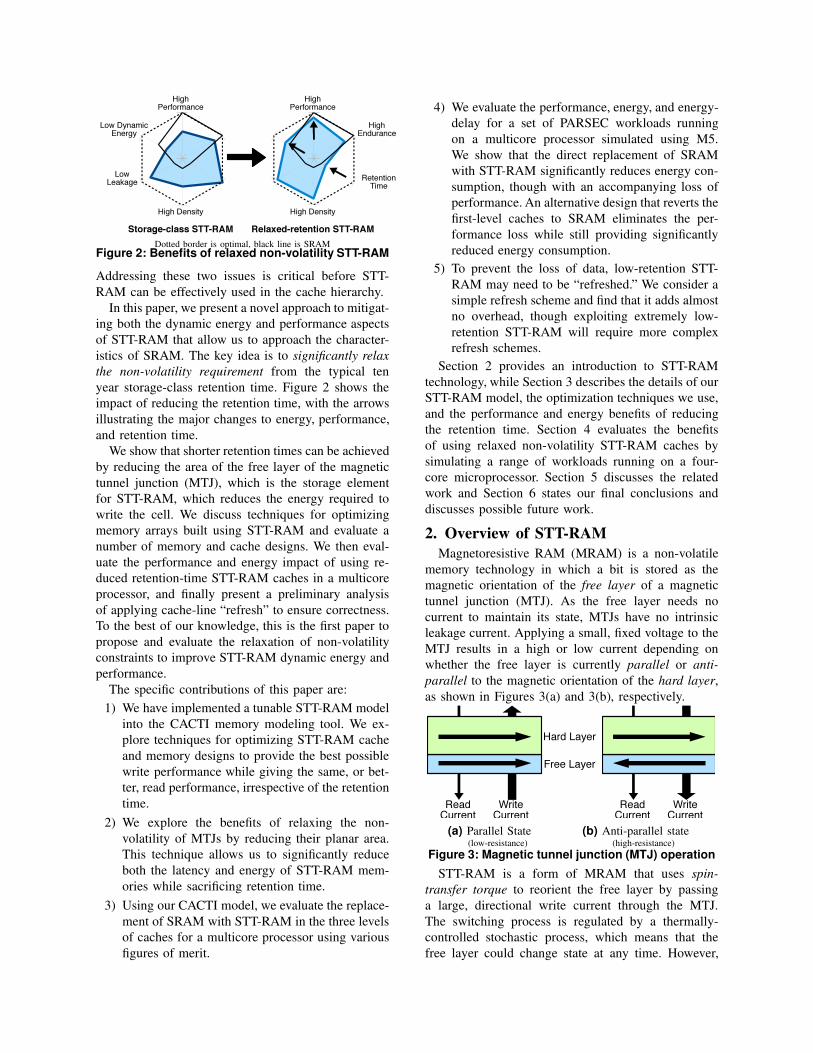
Dotted border is optimal, black line is SRAMFigure 2: Benefits of relaxed non-volatility STT-RAM
Addressing these two issues is critical before STT-
RAM can be effectively used in the cache hierarchy.
In this paper, we present a novel approach to mitigat-
ing both the dynamic energy and performance aspects
of STT-RAM that allow us to approach the character-
istics of SRAM. The key idea is to significantly relax
the non-volatility requirement from the typical ten
year storage-class retention time. Figure 2 shows the
impact of reducing the retention time, with the arrows
illustrating the major changes to energy, performance,
and retention time.
We show that shorter retention times can be achieved
by reducing the area of the free layer of the magnetic
tunnel junction (MTJ), which is the storage element
for STT-RAM, which reduces the energy required to
write the cell. We discuss techniques for optimizing
memory arrays built using STT-RAM and evaluate a
number of memory and cache designs. We then eval-
uate the performance and energy impact of using re-
duced retention-time STT-RAM caches in a multicore
processor, and finally present a preliminary analysis
of applying cache-line “refresh” to ensure correctness.
To the best of our knowledge, this is the first paper to
propose and evaluate the relaxation of non-volatility
constraints to improve STT-RAM dynamic energy and
performance.
The specific contributions of this paper are:
1) We have implemented a tunable STT-RAM model
into the CACTI memory modeling tool. We ex-
plore techniques for optimizing STT-RAM cache
and memory designs to provide the best possible
write performance while giving the same, or bet-
ter, read performance, irrespective of the retention
time.
2) We explore the benefits of relaxing the non-
volatility of MTJs by reducing their planar area.
This technique allows us to significantly reduce
both the latency and energy of STT-RAM mem-
ories while sacrificing retention time.
3) Using our CACTI model, we evaluate the replace-
ment of SRAM with STT-RAM in the three levels
of caches for a multicore processor using various
figures of merit.
4) We evaluate the performance, energy, and energy-
delay for a set of PARSEC workloads running
on a multicore processor simulated using M5.
We show that the direct replacement of SRAM
with STT-RAM significantly reduces energy con-
sumption, though with an accompanying loss of
performance. An alternative design that reverts the
first-level caches to SRAM eliminates the per-
formance loss while still providing significantly
reduced energy consumption.
5) To prevent the loss of data, low-retention STT-
RAM may need to be “refreshed.” We consider a
simple refresh scheme and find that it adds almost
no overhead, though exploiting extremely low-
retention STT-RAM will require more complex
refresh schemes.
Section 2 provides an introduction to STT-RAM
technology, while Section 3 describes the details of our
STT-RAM model, the optimization techniques we use,
and the performance and energy benefits of reducing
the retention time. Section 4 evaluates the benefits
of using relaxed non-volatility STT-RAM caches by
simulating a range of workloads running on a four-
core microprocessor. Section 5 discusses the related
work and Section 6 states our final conclusions and
discusses possible future work.
2. Overview of STT-RAM
Magnetoresistive RAM (MRAM) is a non-volatile
memory technology in which a bit is stored as the
magnetic orientation of the free layer of a magnetic
tunnel junction (MTJ). As the free layer needs no
current to maintain its state, MTJs have no intrinsic
leakage current. Applying a small, fixed voltage to the
MTJ results in a high or low current depending on
whether the free layer is currently parallel or anti-
parallel to the magnetic orientation of the hard layer,
as shown in Figures 3(a) and 3(b), respectively.
(a) Parallel State (b) Anti-parallel state(low-resistance) (high-resistance)
Figure 3: Magnetic tunnel junction (MTJ) operation
STT-RAM is a form of MRAM that uses spin-
transfer torque to reorient the free layer by passing
a large, directional write current through the MTJ.
The switching process is regulated by a thermally-
controlled stochastic process, which means that the
free layer could change state at any time. However,

Table 1: Example thermal factors (∆) for a range ofretention times at 300 K
Retention time ∆
10 years 40.29
1 year 37.99
1 month 35.52
1 week 34.04
1 day 32.09
1 hour 38.91
1 minute 24.82
1 second 20.72
the MTJ magnetic properties and sizing are selected to
make this unlikely. Performing a write requires holding
the write current for a sufficient amount of time, which
we call the MTJ writetime, to ensure the free layer has
changed state.
MTJ Stability and Retention:
The retention time of a MTJ is a characterization
of the expected time until a random bit-flip occurs
and is determined by the thermal stability of the MTJ.
High stability indicates the cell is unlikely to suffer
from random bit-flips but makes it more difficult to
write, requiring either higher currents or more time.
The stability is estimated by the thermal factor, ∆,
which is calculated from Equation 1 using the volume
(V ), the in-plane anisotropy field (Hk), the saturation
magnetization (Ms), and the absolute temperature in
kelvin (T ) [8].
∆ ∝V ·Hk ·Ms
T(1)
Ic (writetime) = A ·
(
Jc0 +C
writetimeγ
)
(2)
Most research into MTJs has focused on developing
storage-class memory with at least a 10 year reten-
tion time at room temperature, and many projections
assume ∆ > 60 to ensure high-reliability at a range
of operating temperatures [2], [6]. Rizzo, et al., use
the formula 1ns · e∆ to estimate the average time to a
MTJ bit flip, which we used to calculate the minimum
thermal factors for the range of retention times shown
in Table 1 [19]. Simply increasing the temperature
from room temperature (300K) to 350K, typical for a
performance microprocessor, can reduce the retention
time to less than a month, while halving the volume
of the free layer can reduce it to mere seconds. By
shrinking an existing MTJ design and taking a hit to
retention time, we can gain the benefits of increased
storage density and reduced write currents.
MTJ Switching Performance:
As we are looking to replace SRAM-based designs,
we look only at using the high-speed precessional
switching mode of STT-RAM that occurs for write-
times less than ≈ 3ns. We characterize the write
current in this region using Equation 2, which we have
adapted from Raychowdhury, et al. [18]. The critical
current density at zero temperature, Jc0, is a figure of
merit for MTJ designs and primarily depends on the
vertical structure and magnetic properties of the MTJ.
We model a STT-RAM MTJ demonstrated by Diao,
et al., that uses two pinned layers with MgO barriers
and CoFeB magnetic materials to achieve an average
Jc0 of 1 MA/cm2, as compared to 2–3 MA/cm2 or more
for single-barrier designs [9]. We performed Monte-
Carlo simulation on this MTJ design for precessional
switching writetimes (from 3 ns to approaching zero) to
determine values for the fitting constants C and γ . The
relative independence of the cross-sectional area of the
free layer, A, allows us to directly reduce the required
write current at the cost of exponentially reducing the
retention time. As a baseline for STT-RAM, we have
conservatively estimated ∆ to be 36 for the design
given by Diao, et al., so we increase the area from
28F2 to 32F2 for a 32 nm process to ensure 10 year
retention time at room temperature.
3. Designing Caches with STT-RAM
We have integrated the analytic model of the MTJ
write current dependence on writetime presented in
Section 2 into CACTI 6.5, the current version of a
widely used tool for estimating the latency, area, and
energy consumption of caches and memories [14],
[21]. We model the SRAM and peripheral circuitry
using the 32 nm ITRS roadmap process integrated into
CACTI [1].
We next describe the parameterization of the an-
alytic MTJ model and our modeling of STT-RAM
circuitry in Section 3.1. Section 3.2 then discusses
two approaches to optimizing the STT-RAM latency,
and Section 3.3 shows the performance improvements
possible by reducing the non-volatility of the MTJs.
Section 3.4 shows the tradeoffs between these different
approaches for replacing SRAM with STT-RAM in the
cache hierarchy of a modern multicore processor.
3.1. STT-RAM Modeling
The analytic MTJ model is fully parameterized to
allow exploring a wide range of designs. We use the
desired planar MTJ area to calculate the area of the
elliptical free layer, while maintaining an aspect ratio
of ≈ 2 : 1. Combining this area with the temperature,
Jc0, and the fitting constants from Section 2 gives us ∆
and the retention time. Given values for the MTJ pa-
rameters, we can then model the STT-RAM cell within
CACTI using the implementation details for reads and
writes given below. Using the output from CACTI,
we then manually tune the MTJ writetime to give the
desired performance and energy characteristics.
Read Operations:
A small voltage (< 0.5V) is applied across the
bit cell to sense the data stored in the MTJ, which

Figure 4: MTJ read sensing circuit
is compared to the average of two reference MTJ
cells. Figure 4 shows the circuit we use to adapt the
current-based operation of the MTJs to the voltage-
based senseamp modeled in CACTI [15]. One of the
reference cells is in the parallel (low resistance) state
while the other is in the anti-parallel (high resistance)
state. After the circuit has stabilized, the current pass-
ing through them is the harmonic mean of the parallel
and anti-parallel cell read currents and is mirrored by
the three PMOS transistors at the top of the circuit.
The inputs to the senseamp will measure the voltage
across the PMOS transistors connected to the test cell
and to the anti-parallel reference cell. The clamping
limits the bitline voltage to improve performance and
reliability.
0.1 0.2 0.3 0.4 0.5 0.6 0.7Read Voltage [V]
0.00
0.05
0.10
0.15
0.20
0.25
Read
late
ncy [
ns]
Figure 5: Read latency against read voltage for a128×8b STT-RAM memory
We modeled this circuit using SPICE at 45 nm and
found it to require ≈ 50ps for stabilization. As this
is a conservative estimate for the delay at 32 nm, we
include it into CACTI as part of the senseamp delay.
We also incorporate the read energy and area of two
reference cells per senseamp. Figure 5 demonstrates
the dependence of read latency on the MTJ read volt-
age. Raising the read voltage increases the probability
of read disturbs, as discussed in Section 2, and, for the
MTJ we model, voltages above 0.5V will significantly
reduce the reliability. The senseamp requires ≈ 0.1V
to ensure proper detection, but this gives 20% slower
reads than 0.6V. We use a read voltage of 0.3V
to minimize the impact on both performance and
reliability, giving reads only 3% slower than at 6 V.
Write Operations:
STT-RAM cells typically use an access transistor
to reduce the overall energy and to prevent write
disturbs [8]. Each cell is connected to both a bitline
and a senseline, as shown on the left of Figure 4, which
are isolated from the read circuitry during a write. The
high write currents involved in fast-switching STT-
RAM require that each bitline have dedicated write
circuitry, so we disallow CACTI from performing
bitline multiplexing. CACTI models the latency and
energy required to initiate a MTJ write operation
to which we add the time and energy necessary to
perform precessional switching at the desired speed.
We determine the sizing for the MTJ access transistor
using the MTJ write current and the high-performance
ITRS transistor scaling roadmaps [1].
Small Arrays:
Ideally, our model should scale from the small
structures within the processing cores to the main
memory. However, the STT-RAM model has 50%
slower reads than SRAM for a 128 B array, as shown
in Figure 6. It shows the read latency for a range of
small memory arrays using a 1 ns MTJ writetime. The
gap between STT-RAM and SRAM, which is just over
60 ps, remains relatively constant as the capacity is
increased, and it is actually dominated by the MTJ
read sensing circuit described earlier in this Section.
Alternative models, such as the lookup tables used by
Guo, et al., are necessary to build small, high-speed
arrays, such as those found within the core [11]. As
such, we focus on replacing the SRAM found in the
data arrays of the cache hierarchy.
128 B 256 B 512 B 1024 B 2 kB 4 kBCapacity
0.00
0.05
0.10
0.15
0.20
0.25
Read
late
ncy [
ns]
SRAM STT-RAM
Figure 6: Read latencies for small memories with 8 Bline size
Initial Results:
We allow CACTI to freely vary the internal organi-
zation to optimize for (in order of importance): (i) read
latency, (ii) leakage power, (iii) area, (iv) read energy,
and (v) cycle time. The difference between the write
latency and energy and the read latency and energy is
dominated by the write current and writetime, so we
exclude them from CACTI’s automated optimization
procedure. We fix the MTJ planar area and keep the
read voltage at 0.3 V, as previously described, while
varying the MTJ writetime within the precessional
switching mode from 0.1 ns to 3 ns by steps of 50 ps.
Figures 7(a) and 7(b) show the read and write
latency, respectively, plotted against the MTJ writetime
for a 1 MB memory array. The jumps in the curves
are caused by CACTI optimizing the internal array
organization as the writetime is changed. As the pe-
ripheral circuitry is largely shared between reads and

0.5 1.0 1.5 2.0 2.5 3.0MTJ Writetime [ns]
0.0
0.5
1.0
1.5R
ead
late
ncy [
ns]
SRAM STT-RAM
(a) Read latency
0.5 1.0 1.5 2.0 2.5 3.0MTJ Writetime [ns]
0.0
0.5
1.0
1.5
2.0
2.5
3.0
3.5
Wri
te late
ncy [
ns]
SRAM STT-RAM
(b) Write latency
Figure 7: Latency against MTJ writetime for a 1 MBmemory with 64 B line size
writes, the write latency can be estimated as the read
latency plus the MTJ writetime. The horizontal dashed
lines are the latency for a high-performance SRAM
cache, and the heavy vertical line at 1.35 ns shows the
STT-RAM design that matches the SRAM read latency
while minimizing the write latency. Increasing the MTJ
writetime beyond this threshold will give faster reads
than SRAM at the cost of even slower writes, while
reducing it gives faster writes at the cost of slower
reads. Unfortunately, these results show that STT-RAM
is unable match the write latency of SRAM, regardless
of how slow reads are made. Since a tradeoff must be
made between read and write latency, we next explore
different techniques for optimizing the design of STT-
RAM-based caches and memories.
3.2. Optimizing STT-RAM Performance
As seen in Section 3.1, STT-RAM cannot match
the write latency of SRAM. To improve on those
results, we leverage the fact that latency variations
less than one clock cycle will not affect performance,
as most caches operate synchronously with the pro-
cessor’s clock. Thus, matching the read performance
of a SRAM design requires only that the cycle-based
read latency be the same. Below, we describe two
procedures that match or exceed the read performance
of SRAM while maximizing the write performance. In
this paper, we use a somewhat aggressive clock fre-
quency of 4 GHz (current processors top out at around
0.50 0.75 1.00 1.25 1.50MTJ Writetime [ns]
0.50
0.75
1.00
1.25
Read
late
ncy [
ns]
SRAM STT-RAM
(a) Read latency
0.50 0.75 1.00 1.25 1.50MTJ Writetime [ns]
1.25
1.50
1.75
2.00
2.25
Wri
te late
ncy [
ns]
SRAM STT-RAM
(b) Write latency
Figure 8: Latency against MTJ writetime for a 1 MBmemory with 64 B line size
3.5 GHz). Howerver, the procedures we describe below
can be applied to any clock speed.
Write Optimization:
We first maximize our write performance (that is, the
cycle-based write latency) while matching the SRAM
read performance. The first step is to increase the
read latency, thus reducing the write latency, with-
out impacting the performance of reads, as shown
in Figure 8(a). The vertical dashed line shows the
original design choice from Section 3.1 while the
vertical solid line shows the design chosen by this first
step, with the arrow showing the direction of travel.
Figure 8(b) shows the second step, where we increase
the MTJ writetime to find the Pareto optimal point,
thus reducing the read energy by 5% and the write
energy by 3% while giving the same read and write
performance. The vertical dashed lines again show the
obsolete designs, while the solid vertical line shows
the final write-optimized design chosen by following
the arrow. Overall, this procedure reduces the effective
write latency by three cycles compared to the naive
approach used in Section 3.1 (six cycles instead of
nine), while giving the same effective read latency of
four cycles.
Read Optimization:
The write optimization of the previous section at-
tempts to minimize the negative performance impact
of switching to STT-RAM by matching the SRAM
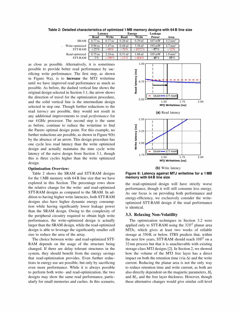
Table 2: Detailed characteristics of optimized 1 MB memory designs with 64 B line size
.
Latency Energy Leakage
Read Write Read Write Power Area
SRAM 0.77 ns 0.77 ns 0.28 nJ 0.29 nJ 447 mW 4.2 mm2
Write-optimized 0.96 ns 1.47 ns 0.48 nJ 3.38 nJ 192 mW 4.7 mm2
STT-RAM +25% +90% +70% +1072% −57% +12%
Read-optimized 0.75 ns 2.24 ns 0.31 nJ 1.68 nJ 105 mW 1.9 mm2
STT-RAM −3% +190% +11% +484% −45% −55%
as close as possible. Alternatively, it is sometimes
possible to provide better read performance by sac-
rificing write performance. The first step, as shown
in Figure 9(a), is to increase the MTJ writetime
until we have improved read performance as much as
possible. As before, the dashed vertical line shows the
original design selected in Section 3.1, the arrow shows
the direction of travel for the optimization procedure,
and the solid vertical line is the intermediate design
selected in step one. Though further reductions to the
read latency are possible, they would not result in
any additional improvements to read performance for
our 4 GHz processor. The second step is the same
as before, continue to reduce the writetime to find
the Pareto optimal design point. For this example, no
further reductions are possible, as shown in Figure 9(b)
by the absence of an arrow. This design procedure has
one cycle less read latency than the write optimized
design and actually maintains the nine cycle write
latency of the naive design from Section 3.1, though
this is three cycles higher than the write optimized
design.
Optimization Overview:
Table 2 shows the SRAM and STT-RAM designs
for the 1 MB memory with 64 B line size that we have
explored in this Section. The percentage rows show
the relative change for the write- and read-optimized
STT-RAM designs as compared to the SRAM. In ad-
dition to having higher write latencies, both STT-RAM
designs also have higher dynamic energy consump-
tion while having significantly lower leakage power
than the SRAM design. Owing to the complexity of
the peripheral circuitry required to obtain high write
performance, the write-optimized design is actually
larger than the SRAM design, while the read-optimized
design is able to leverage the significantly smaller cell
size to reduce the area of the array.
The choice between write- and read-optimized STT-
RAM depends on the usage of the structure being
changed. If there are delay tolerant structures in the
system, they should benefit from the energy savings
that read-optimization provides. Even further reduc-
tions in energy use are possible, but only by sacrificing
even more performance. While it is always possible
to perform both write- and read-optimization, the two
designs may show the same read performance, partic-
ularly for small memories and caches. In this scenario,
1.50 1.75 2.00MTJ Writetime [ns]
0.50
0.75
1.00
Read
late
ncy [
ns]
SRAM STT-RAM
(a) Read latency
1.50 1.75 2.00MTJ Writetime [ns]
1.75
2.00
2.25
2.50
Wri
te late
ncy [
ns]
SRAM STT-RAM
(b) Write latency
Figure 9: Latency against MTJ writetime for a 1 MBmemory with 64 B line size
the read-optimized design will have strictly worse
performance, though it will still consume less energy.
As our focus is on providing both performance and
energy-efficiency, we exclusively consider the write-
optimized STT-RAM design if the read performance
is identical.
3.3. Relaxing Non-Volatility
The optimization techniques in Section 3.2 were
applied only to STT-RAM using the 32F2 planar area
MTJs, which gives at least two weeks of reliable
storage at 350K or below. ITRS predicts that, within
the next few years, STT-RAM should reach 10F2 on a
32 nm process but that it is unachievable with existing
storage-class MTJ designs [2]. In Section 2, we showed
how the volume of the MTJ free layer has a direct
impact on both the retention time (via ∆) and the write
current. Reducing the planar area is not the only way
to reduce retention time and write current, as both are
also directly dependent on the magnetic parameters, Hk
and Ms, and the free layer thickness. However, though
these alternative changes would give similar cell-level

0.4 0.8 1.2 1.6 2.0MTJ Writetime [ns]
0.50
0.75
1.00
1.25
1.50
1.75R
ead
late
ncy [
ns]
SRAM
32F2
19F2
10F2
WO
RO
(a) Read latency
0.4 0.8 1.2 1.6 2.0MTJ Writetime [ns]
1.00
1.25
1.50
1.75
2.00
2.25
2.50
2.75
Wri
te late
ncy [
ns]
SRAM
32F2
19F2
10F2
WO
RO
(b) Write latency
Figure 10: Latency against MTJ writetime for a 1 MBmemory with 64 B line size10F2 , 19F2 , 32F2 are STT-RAM designs, WO/RO indicates the write- and
read-optimized design points, respectively.
benefits as the 10F2 cells we model here, the larger
planar area could limit the total impact the latency,
energy, and area of the resulting design.
Reducing the planar area from 32F2 to 19F2 reduces
the retention time at 350K to little more than one
second — a dramatic reduction. Reducing it further
to 10F2 reduces the retention time to only 56 µs.
The downside, particularly for 10F2 designs, is that
reducing the retention time may require a form of
refreshing or error scrubbing to ensure correctness.
However, unlike DRAM, it is unnecessary to write the
data line if no error is detected, as STT-RAM has non-
destructive reads.
Figures 10(a) and 10(b) show the read and write
latency plotted against the MTJ writetime for these
three MTJ planar areas, with the SRAM design again
included for comparison. The write-optimized designs
are marked with circles, while the read-optimized
designs are marked with diamonds, and the 10F2
design has the same write- and read-optimized design
point. Both the 19F2 and 10F2 write-optimized designs
are able the improve write performance (only one
cycle slower than SRAM). The 19F2 read-optimized
design improves the read performance by one cycle,
obtains the same write performance as the 32F2 write-
optimized design from Section 3.2, all while reducing
the read and write energy by 35% and 69%, respec-
tively. The 10F2 design has one cycle faster read and
one cycle slower write performance than SRAM, while
using even less dynamic energy than either of the 19F2
designs (though leakage power is slightly higher).
3.4. STT-RAM Handbook
Sections 3.2 and 3.3 described orthogonal changes
to the STT-RAM cell design that significantly improve
the performance and energy of the STT-RAM designs
over the naive implementation. However, none of these
techniques are able to match the write performance
of SRAM. We must therefore weigh the benefits to
energy consumption against the impact on performance
(positive or negative). To perform this evaluation, we
now consider a three-level, on-chip cache hierarchy
for a four-core processor similar to Intel’s Core i7 or
AMD’s Phenom X4 processors, with the parameters
shown in Table 3, operating at 4GHz, as used in
previous Sections. All caches feature single-bit error
correction and we use high-performance transistors for
the peripheral circuitry and tag array except for the SL3
cache, which uses low power transistors and serialized
tag lookup to help reduce energy consumption. The re-
duction in area that the density of STT-RAM affords is
limited by the size of the peripheral circuitry necessary
to enable high-speed writes.Table 3: Cache configurations
Structure Size Associativity Banks
IL1 32 kB 4-way 1 bank
Private (per-core) level 1 instruction cache
DL1 32 kB 8-way 1 bank
Private (per-core) level 1 data cache
UL2 256 kB 8-way 1 bank
Private (per-core) level 2 unified cache
SL3 8 MB 16-way 4 banks
Shared level 3 unified cache
Figure 11 compares the STT-RAM designs to the
SRAM designs for the IL1 cache. Each of the six
properties ((i) read latency, (ii) write latency, (iii) read
energy, (iv) write energy, (v) leakage power, and
(vi) area) have been normalized against the SRAM
design (shown as the darkened ring at 100%) and
plotted on an inverted log scale. The ideal universal
memory would beat SRAM on every metric and would
thus fill the majority of the chart area. Read opti-
mization does not provide improved read performance
for either the IL1 or DL1, so we remove them from
consideration. Figure 11(a) shows that while the 32F2
design reduces leakage power and area the high write
current dramatically increases the write latency and
energy. The 10F2, shown in Figure 11(c), approaches

(a) 32F2 WO (b) 19F2 WO (c) 10F2 WO
Figure 11: Comparison of IL1 STT-RAM designs against the SRAM baseline
(a) 32F2 WO (b) 19F2 WO (c) 10F2 WO
(d) 19F2 RO (e) 10F2 RO
Figure 12: Comparison of UL2 STT-RAM designs against the SRAM baseline
the write energy and latency of SRAM while signifi-
cantly reducing all other properties. The 19F2 design
lies roughly half-way between the other two, though
its read energy is at parity with SRAM. The DL1 has
similar characteristics, though the higher associativity
increases the latency, energy, and area.
As expected, relaxing the non-volatility also im-
proves the write latency, read energy, and write en-
ergy for the UL2 as well, as shown in Figure 12,
though there is no read-optimized 32F2 design. Com-
paring the read-optimized 19F2 and 10F2 designs (Fig-
ures 12(d) and 12(e)) to the write-optimized designs
(Figures 12(b) and 12(c)) shows that there is a definite
tradeoff between write latency and all other character-
istics. The read-optimized 10F2 design exceeds SRAM
in every way except write latency, in which it is sig-
nificantly worse than the write-optimized version. The
SL3 shows these same trends and tradeoffs, though all
three MTJ sizings have read-optimized counterparts.
We are unable to completely eliminate the write
latency gap between STT-RAM and SRAM. However,
the significant improvements our optimizations and
relaxing non-volatility has provided may prove enough
to match the performance of SRAM, though possibly
not at the DL1 (which is the most write intensive).
Furthermore, the massive improvements to dynamic
energy and leakage possible with STT-RAM should
significantly reduce the total energy consumption. We
next perform architectural simulations to evaluate the
impact on performance and total energy and to deter-
mine whether write- or read-optimized STT-RAM is
more effective in practice.
4. Migrating to STT-RAM-based Caches
We now perform an architecture level evaluation
of the cache designs modeled in Section 3.4. We
describe our simulation infrastructure and workloads
in Section 4.1, compare the write- and read-optimized
designs for each of the three retention times in Sec-
tion 4.2, and look at the benefits of hybrid designs that
combine both SRAM and STT-RAM in Section 4.3.
Low-retention time STT-RAM is likely to have random
bit-flips, so we consider the impact of a simple refresh
policy on energy-efficiency in Section 4.4.

Table 4: Workload characteristicsInstruction Read & Write Read-Write
Workload Count Volume Ratio Application Description
blackscholes 817 M 11 GB 2.8 : 1 Computational finance
canneal 495 M 5.7 GB 5.9 : 1 EDA Kernel
rtview 5.3 B 100 GB 5.6 : 1 Real-time raytracing
x264 8.5 B 67 GB 7.3 : 1 Video encoder
facesim 24 B 288 GB 3.1 : 1 Facial animation
4.1. Experimental Setup
We model a 4 GHz processor with four out-of-order
cores using M5 [5]. We assume that main memory has
a fixed 200 cycle latency and model the three-level
cache configuration previously described in Table 3.
We have modified the simulator to model cache banks
and to use the subbank write buffering proposed by
Guo, et al. [11]. Once the MTJ write operation has
been initiated within a subbank, the write buffer main-
tains the data to be written and the bank is free to
handle a new request. As long as subsequent requests
access different subbanks, we are able to overlap
the requests and ameliorate the latency gap between
reads and writes. CACTI calculates the number of
subbanks for each cache design, but, in general, the
write-optimized STT-RAM designs have twice as many
subbanks as read-optimized ones.
We evaluate our STT-RAM designs using three
metrics: (i) speedup, (ii) total energy used by the
caches, and (iii) energy-delay (E-D) product for a set of
multithreaded workloads drawn from the PARSEC 2.0
benchmark suite [3], [4]. Each workload uses one
thread per core (four threads total) and is run using the
small input size, which gives the characteristics shown
in Table 4. To permit direct comparison between work-
loads, we normalize each metric against the SRAM-
based design. Simulation statistics are collected only
for the parallel portion of the workload, skipping the
initialization and termination phases. We estimate the
leakage power by multiplying the value determined in
Section 3.4 by the total execution time. We calculate
the dynamic energy consumption for each cache using
the total number of reads, writes, and fills combined
with the energy per operation from before. However,
as most of the writes to the DL1 cache will be ≈ 8B in
size, we improve the estimate for write energy by using
the average number of bytes written (either by a write
or by a fill) to interpolate between the energy per write
operation(which assumes 64 B are being written) and
the energy per read operation (a conservative estimate
for writing zero bytes).
4.2. Direct replacement of SRAM with STT-RAM
We start by replacing all three levels of cache with
the STT-RAM-based designs from Section 3.4. The
performance of this aggressive change is shown in
Figure 13, with each bar representing the speedup
0
0.1
0.2
0.3
0.4
0.5
0.6
0.7
0.8
0.9
1
black-scholes
canneal rtview x264 facesim Geometricmean
No
rma
lize
d S
pe
ed
up
Benchmarks
SRAM32F
2-WO
32F2-RO
19F2-WO
19F2-RO
10F2-WO
10F2-RO
Figure 13: Performance of write- and read-optimizedSTT-RAM cache hierarchies
(Normalized to SRAM baseline.)
relative to the SRAM cache baseline, and a speedup
of less than one indicating reduced performance. Each
bar represents replacing SRAM with the stated variant
of STT-RAM; WO indicates the exclusive use of
write-optimized STT-RAM, while RO indicates the
use of read-optimized STT-RAM for the UL2 and
SL3 caches. However, the 32F2-RO design uses the
write-optimized UL2 design since the read-optimized
version has no performance benefits, as described in
Section 3.4.
As expected, the increased write latency has a
significant negative impact on performance for most
of the workloads, though it is almost eliminated by
relaxing the retention time. Despite having higher write
latencies, the read-optimized STT-RAM designs do not
show any significant difference in performance from
the write-optimized designs, and they even achieve
speedup (for x264 and canneal) using the 10F2 de-
signs! This improvement is due to latency sensitivity
in the UL2 caches, as indicated by the fact that the
read- and write-optimized 32F2 designs give identical
performance.
Figures 14(a)–14(e) show the total energy for each
design, as well as the breakdown into read, write, and
leakage energy. As expected, STT-RAM reduces the
leakage power by more than 3×. On average, it uses
only 31% of the total energy for the 32F2 designs and
21% for the 10F2 designs. As the first-level caches
dominate the read and write energy, the slight reduction
in energy per read operation at that level results in a
significant reduction in the total read energy (almost
halved for the 10F2-RO design), regardless of retention
time. However, the write energy for canneal is almost
5× that of SRAM for the 32F2 designs, 2× for 10F2,
and still increased by 13% for 10F2. Overall, the

0 0.1 0.2 0.3 0.4 0.5 0.6 0.7 0.8 0.9
1
SRAM32F
2 -WO
32F2 -R
O
19F2 -W
O
19F2 -R
O
10F2 -W
O
10F2 -R
O
No
rma
lize
d e
ne
rgy
(a) blackscholesSRAM
32F2 -W
O
32F2 -R
O
19F2 -W
O
19F2 -R
O
10F2 -W
O
10F2 -R
O
(b) cannealSRAM
32F2 -W
O
32F2 -R
O
19F2 -W
O
19F2 -R
O
10F2 -W
O
10F2 -R
O
(c) facesimSRAM
32F2 -W
O
32F2 -R
O
19F2 -W
O
19F2 -R
O
10F2 -W
O
10F2 -R
O
(d) rtviewSRAM
32F2 -W
O
32F2 -R
O
19F2 -W
O
19F2 -R
O
10F2 -W
O
10F2 -R
O
ReadWrite
Leakage
(e) x264
Figure 14: Energy consumption of write- and read-optimized STT-RAM cache hierarchies(Normalized to SRAM baseline.)
32F2 designs do increase the write energy by 46%
on average, but the 19F2 and 10F2 designs are able to
reduce it by at least 12%.
The normalized energy-delay for these designs is
nearly identical to the normalized energy, as the re-
duction in leakage alone far outweighs the reduction in
performance. Overall, the massive reduction in energy
(particularly leakage) makes a strong case for using
STT-RAM caches, though only the 10F2 designs are
able to consistently match the performance of SRAM.
Despite having higher write latencies, the benefits of
reducing the read latency and energy consumption
allows the read-optimized UL2 and SL3 cache designs
to be more energy-efficient.
4.3. SRAM and STT-RAM Hybrid
The performance statistics from the previous simu-
lations showed that the DL1 caches have more than
two orders-of-magnitude more writes and fills than
the UL2 caches, while the SL3 has roughly the same
number as the four UL2 caches combined, indicating
that the DL1 is the most write-latency sensitive cache.
Though the IL1 caches have far fewer writes than
the DL1 caches, delays in handling IL1 misses can
have a significant impact on processor performance
as well. As the first-level caches represent only a
fraction of the total power, negating the performance
slowdown should improve the performance and could
also improve the energy-efficiency. To test this, we
took the read-optimized designs used in Section 4.2
and reverted both the DL1 and IL1 caches to use
SRAM.
As a result, the 32F2 hybrid design reduces the peak
slowdown from 23% to 3%, while the 19F2 and 10F2
hybrid designs meet or exceed the full performance
of the SRAM baseline in all but one instance. How-
ever, the hybrid designs generally have lower energy-
efficiency than the pure STT-RAM designs, though still
far better than SRAM, as shown in Figure 15. The per-
formance improvement does reduce the leakage energy
for the second and third level caches. However, the
first-level caches dominate the dynamic read and write
energy of the cache hierarchy, and reverting them to
SRAM thus negates the improvements to both dynamic
0
0.1
0.2
0.3
0.4
0.5
0.6
0.7
0.8
0.9
1
black-scholes
canneal rtview x264 facesim GeometricMean
No
rmali
zed
en
erg
y-d
ela
y p
rod
uc
t
Benchmarks
SRAM32F
2-RO
SRAM+32F2-RO
19F2-RO
SRAM+19F2-RO
10F2-RO
SRAM+10F2-RO
Figure 15: Energy-efficiency of hybrid SRAM andSTT-RAM cache hierarchies
(Normalized to SRAM baseline.)
and leakage energy. The STT-RAM IL1 caches give a
16% (for 32F2) to 52% (for 10F2) average reduction in
total energy, and the DL1 caches give a 34% to 48%
average reduction. For the SRAM+32F2-RO design,
the 8% increase in average total energy is mitigated
by a matching 8% increase in average performance.
The performance improvement for the 19F2 and 10F2
designs is unable to overcome their respective 15%
and 24% increase in average total energy. Though
pure STT-RAM hierarchies provide the best energy-
efficiency, further improvements to the use of STT-
RAM for first-level caches are necessary to completely
bridge the performance gap.
4.4. Refreshing Non-volatile Memory
We have shown that reducing the retention time
of STT-RAM caches improves both performance and
energy efficiency. Thus far, however, we have ne-
glected the possible correctness issues that may arise
due to random bit-flips. The use of single-bit error
correction facilitates the implementation of a refresh-
like operation that reads the contents of a line and
writes it back after performing error correction. As
previously mentioned, the non-destructive nature of
STT-RAM reads makes it unnecessary to perform the
writeback if no error is detected.
We now present a simple, DRAM-style refresh pol-
icy that iterates through each line, refreshing them
in-turn, and we conservatively assume the worst-case
scenario in which every refresh operation detects an
error and requires a writeback. The refresh interval

is calculated to guarantee that every line will be
“refreshed” within the retention time interval. Even at
350 K, the 32F2 design can retain data for more than
two weeks, negating the need for a hardware-based
cache refresh policy. The 19F2 designs retain data for
more than 30 seconds at room temperature and slightly
more than one second at our operating temperature,
still far larger than the standard DRAM refresh interval
of 64 ms.
However, the 10F2 design has only 345 µs retention
time at room temperature and 56 µs at 350 K. This cre-
ates a problem for the SL3 at the operating temperature
since it must refresh a line every 427 ps. Each bank
must start a refresh every 1.7 ns, which is less than
the write latency and only slightly more than the read
latency. Though possible, this would leave almost no
time to service actual requests, negating any benefits
to the read and write latency. Because of the excessive
refresh rate, we exclude the 10F2 SL3 design from
our evaluation of refresh. We can continue using the
microsecond retention time STT-RAM for the UL2, as
the lower capacity gives a refresh interval of 13.7ns.
For comparison, the 19F2 SL3 has a refresh interval
of 33 µs.
0
0.1
0.2
0.3
0.4
0.5
0.6
0.7
0.8
0.9
1
black-scholes
canneal rtview x264 facesimNo
rmali
zed
en
erg
y-d
ela
y p
rod
uct
Benchmarks
SRAMSRAM+32F
2-RO
SRAM+19F2-RO
SRAM+19F2-RO+REF
SRAM+10F2-RO
SRAM+10/19F2-RO+REF
Figure 16: Impact of STT-RAM refreshing on theenergy-delay product
(Normalized to SRAM baseline.)
We model two designs using the DRAM-style re-
fresh policy: the first using 19F2 for both the UL2
and SL3 caches (SRAM+19F2-RO+REF), while the
second switches the UL2 caches to the 10F2 design
(SRAM+10/19F2-RO+REF). These designs are based
on the hybrid designs from Section 4.3 to provide
a consistent performance reference. Figure 16 shows
the normalized energy-delay product for these designs
as well as the original hybrid designs. As expected,
the energy and performance impact of performing
refreshing is negligible for the 19F2 designs. Despite
the addition of refresh operations, which take time
and consume energy, the 19F2 design continues to
provide improved energy efficiency over the 32F2-
based design. However, switching the UL2 to 10F2 in-
creases the energy while providing no performance im-
provement which, overall, slightly reduces the energy-
efficiency. Though unsuitable for use with the DRAM-
style refresh policy, the hybrid combination of SRAM-
based first-level caches with the 10F2 read-optimized
STT-RAM still has 15% better efficiency than 19F2
and is almost 20% better than the storage-class 32F2.
We have demonstrated that the 19F2 STT-RAM
cache designs using a simple refresh policy can im-
prove performance and reduce energy consumption
over the more direct implementation of 32F2 STT-
RAM designs while providing significantly higher
densities. Improving the density of on-chip memory
is important as it facilitates the continued scaling of
multicore processors [23]. Planar areas other than 10F2
and 19F2 are possible, and it may be necessary to
tune the retention time for each structure to achieve
the best balance between performance and total energy
consumption. The use of a more advanced design, such
as a policy that only refreshes dirty cache lines or a
multi-bit error-correcting code, could make ultra-low
retention designs practical.
5. Related Work
STT-RAM is a promising new technology that has
the potential to become a truly universal memory.
Existing studies have looked at using STT-RAM within
the processor to exploit the leakage power benefits of
STT-RAM [6], [11], [17]. Guo, et al., designed combi-
national logic and on-chip caches using scalable RAM
blocks, look-up tables (LUTs) and by re-architecting
the pipeline using STT-RAM [11]. They use a subbank
write buffering policy to increase write throughput and
to allow read-write bypassing in order to hide the high
write latency of storage-class STT-RAM.
Rasquinha, et al., address the high write energy of
STT-RAM by using policies that prevent premature
eviction of lines from higher level caches to lower
level caches [17]. They propose a new replacement
algorithm to increase the residency of dirty lines at
the penalty of increasing the miss rate. Other studies
have used the predecessor to STT-RAM, MRAM, to
design memory systems that take advantage of their
low leakage [7], [20], [22]. However, these designs
circumvent the write energy and write latency penalty
of STT-RAM memory technology by changing the
microarchitecture rather than the memory cells them-
selves. Unlike previous work, we show methods for
adapting STT-RAM to make it suitable as a drop in
replacement for SRAM by reducing the latency and
energy.
Cache line refresh policies have been evaluated
by Liang, et al., in the context of 3T-1D memory
arrays [13]. They evaluated refresh policies and re-
placement algorithms to handle the limited retention
of 3T-1D cells, and Emma, et al., make the case for

reducing main memory DRAM power consumption
by reducing the refresh intervals [10]. Less intrusive
retention-aware policies are feasible for STT-RAM
because the refresh interval required can be tuned for
the memory structure’s usage patterns and size.
6. Conclusions and Future Work
The memory system (and the cache hierarchy in
particular) has a large impact on the performance of
applications running on multicore processors. While
SRAM has been the technology of choice for caches,
its excessive leakage power consumption poses a sig-
nificant challenge. The high endurance, density, and
low leakage of STT-RAM make it an attractive mem-
ory technology to use in lieu of SRAM, though STT-
RAM poses its own challenges with regard to dynamic
energy and slow write latencies.
In this paper, we have shown that it is possible
to address these issues by redesigning the MTJ to
use a smaller free layer, though this entails sacrificing
retention time. Using CACTI and the STT-RAM model
we have developed, we have shown how such cells
can be designed and optimized to provide improved
read or write performance while also reducing the
dynamic energy when compared to storage-class STT-
RAM. Using M5 and a set of PARSEC workloads, we
have evaluated the performance, energy, and energy-
delay of incorporating such caches into the memory
hierarchy of a multicore processor.
We have shown that a STT-RAM cache hierarchy
provides the best energy-efficiency and that using a
hybrid design with SRAM L1 caches ensures the
same performance as an all-SRAM hierarchy. We then
provided a preliminary evaluation of a simple cache-
line refresh scheme that prevents the premature loss of
data from the STT-RAM caches and show that it has
only a small impact on the energy-delay product. In
future work, we plan to carry out a more detailed ex-
ploration of refresh techniques and further approaches
to designing low-retention STT-RAM caches.
AcknowledgmentWe thank Eugene Chen from Grandis, and Avik Ghosh,
Kamaram Munira, Jiwei Lu and Stu Wolf from the Universityof Virginia, and the reviewers for their valuable inputs. Thisresearch was supported in part by NSF CAREER AwardCCF-0643925, DARPA’s STT-RAM program, and gifts fromGoogle and HP. Any opinions, findings and conclusions orrecommendations expressed in this material are those of theauthors and do not necessarily reflect the views of DARPA.
References[1] W. Arden, P. Cogez, M. Graef, H. Ishiuchi, T. Osada, J. Moon, J. Roh,
H.-C. Sohn, W. Yang, M.-S. Liang, C. H. Diaz, C.-H. Lin, P. Apte,
B. Doering, P. Gargini et al., International Technology Roadmap
for Semiconductors. http://www.itrs.net/: Semiconductor Industries
Association, 2007.[2] W. Arden, P. Cogez, M. Graef, R. Mahnkopf, , H. Ishiuchi, T. Osada,
J. Moon, J. Roh, C. H. Diaz, B. Lin, P. Apte, B. Doering, P. Gargini
et al., International Technology Roadmap for Semiconductors. http://
www.itrs.net/: Semiconductor Industries Association, 2009.
[3] C. Bienia, S. Kumar, J. P. Singh, and K. Li, “The parsec benchmark
suite: Characterization and architectural implications,” in Proceedings
of the 17th International Conference on Parallel Architectures and
Compilation Techniques, October 2008.
[4] C. Bienia and K. Li, “Parsec 2.0: A new benchmark suite for chip-
multiprocessors,” in Proceedings of the 5th Annual Workshop on
Modeling, Benchmarking and Simulation, June 2009.
[5] N. L. Binkert, R. G. Dreslinski, L. R. Hsu, K. T. Lim, A. G. Saidi, and
S. K. Reinhardt, “The M5 Simulator: Modeling Networked Systems,”
IEEE Micro, vol. 26, no. 4, pp. 52–60, 2006.
[6] E. Chen, D. Apalkov, Z. Diao, A. Driskill-Smith, D. Druist, D. Lottis,
V. Nikitin, X. Tang, S. Watts, S. Wang, S. A. Wolf, A. W. Ghosh,
J. W. Lu, S. J. Poon, M. Stan, W. H. Butler, S. Gupta, C. Mewes,
W. Mewes, and P. B. Visscher, “Advances and future prospects of
spin-transfer torque random access memory,” IEEE Transactions on
Magnetics, vol. 46, no. 6, pp. 1873–1878, 2010.
[7] R. Desikan, C. R. Lefurgy, S. W. Keckler, and D. Burger, “On-chip
mram as a high-bandwidth, low-latency replacement for dram physical
memories,” University of Texas at Austin, Tech. Rep. TR-02-47, 2002.
[8] Z. Diao, Z. Li, S. Wang, Y. Ding, A. Panchula, E. Chen, L.-C.
Wang, and Y. Huai, “Spin-transfer torque switching in magnetic tunnel
junctions and spin-transfer torque random access memory,” Journal of
Physics: Condensed Matter, vol. 19, p. 165209, 2007.
[9] Z. Diao, A. Panchula, Y. Ding, M. Pakala, S. Wang, Z. Li, D. Apalkov,
H. Nagai, A. Driskill-Smith, L.-C. Wang, E. Chen, , and Y. Huai, “Spin
transfer switching in dual MgO magnetic tunnel junctions,” Applied
Physics Letters, vol. 90, p. 132508, 2007.
[10] P. G. Emma, W. R. Reohr, and M. Meterelliyoz, “Rethinking refresh:
Increasing availability and reducing power in dram for cache applica-
tions,” IEEE Micro, vol. 28, no. 6, pp. 47–56, 2008.
[11] X. Guo, E. Ipek, and T. Soyata, “Resistive computation: Avoiding
the power wall with low-leakage, stt-mram based computing,” in
Proceedings of the 37th annual International Symposium on Computer
Architecture, 2010, pp. 371–382.
[12] B. C. Lee, E. Ipek, O. Mutlu, and D. Burger, “Architecting Phase
Change Memory as a Scalable DRAM Alternative,” in Proceedings of
the 36th International Symposium on Computer Architecture, 2009, pp.
2–13.
[13] X. Liang, R. Canal, G.-Y. Wei, and D. Brooks, “Process variation
tolerant 3t1d-based cache architectures,” in Proceedings of the 40th
Annual IEEE/ACM International Symposium on Microarchitecture,
2007, pp. 15–26.
[14] N. Muralimanohar, R. Balasubramonian, and N. P. Jouppi, “CACTI
6.0: A Tool to Model Large Caches,” HP Laboratories, Tech. Rep.
HPL-2009-85, 2009.
[15] S. Natarajan, S. Chung, L. Paris, and A. Keshavarzi, “Searching for
the dream embedded memory,” IEEE Solid-State Circuits Magazine,
vol. 1, no. 3, pp. 34–44, 2009.
[16] M. K. Qureshi, V. Srinivasan, and J. A. Rivers, “Scalable High
Performance Main Memory System Using Phase-Change Memory
Technology,” in Proceedings of the 36th International Symposium on
Computer Architecture, 2009, pp. 24–33.
[17] M. Rasquinha, D. Choudhary, S. Chatterjee, S. Mukhopadhyay, and
S. Yalamanchili, “An energy efficient cache design using spin torque
transfer (stt) ram,” in Proceedings of the 16th ACM/IEEE International
Symposium on Low Power Electronics and Design, 2010, pp. 389–394.
[18] A. Raychowdhury, D. Somasekhar, T. Karnik, and V. De, “Design space
and scalability exploration of 1t-1stt mtj memory arrays in the presence
of variability and disturbances,” in IEEE International Electron Devices
Meeting, 2009, pp. 1 –4.
[19] N. D. Rizzo, M. DeHerrera, J. Janesky, B. Engel, J. Slaughter,
and S. Tehrani, “Thermally activated magnetization reversal in
submicron magnetic tunnel junctions for magnetoresistive random
access memory,” Applied Physics Letters, vol. 80, no. 13, pp.
2335–2337, 2002. [Online]. Available: http://link.aip.org/link/?APL/
80/2335/1
[20] G. Sun, X. Dong, Y. Xie, J. Li, and Y. Chen, “A novel architecture of
the 3D stacked MRAM L2 cache for CMPs,” in Proceedings of the 15th
International Symposium on High Performance Computer Architecture,
February 2009, pp. 239–249.
[21] S. Thoziyoor, N. Muralimanohar, and N. P. Jouppi, “CACTI 5.0,” HP
Laboratories, Tech. Rep. HPL-2007-167, 2007.
[22] X. Wu, J. Li, L. Zhang, E. Speight, R. Rajamony, and Y. Xie, “Hybrid
cache architecture with disparate memory technologies,” in Proceedings
of the 36th International Symposium on Computer Architecture, 2009,
pp. 34–45.
[23] L. Zhao, R. R. Iyer, R. Illikkal, and D. Newell, “Exploring dram cache
architectures for cmp server platforms,” in Proceedings of the 25th
International Conference on Computer Design, 2007, pp. 55–62.