Embed Size (px)
Citation preview
Reliability-Aware Design Method for CMOS Circuits
Theodor Hillebrand, Nico Hellwege, Steffen Paul, Dagmar Peters-DrolshagenInstitute of Electrodynamics and Microelectronic (ITEM.me)
University of Bremen, Germany, +49(0)421/218-62551{hillebrand, hellwege, steffen.paul, peters}@me.uni-bremen.de
Abstract—In this paper a reliability-aware design method
based on the
gm/I
D
-methodology is presented which allows
designers of integrated analog circuits to consider process as well
as environmental variations and aging effects already at early
design stages. Within this method the whole simulation effort is
shifted to a single transistor level. With a generated stochastic
Look-Up table the small signal characteristics of transistors and
circuits can be predicted. Exemplarily, a reliability-aware design
for common source amplifiers is shown and the predicted values
are compared to those from a traditional simulation showing good
data fitting and small deviations.
I. INTRODUCTION
Reliable design flows for integrated CMOS circuits musttake into account all effects that influence whole circuits orseveral single transistors. For larger technology nodes it wassufficient to design a circuit with respect to pure electricalproperties like voltages, currents or capacitance. However, theprogressive downscaling of CMOS transistors necessitates adesign flow that is able to consider both process variationsand time-dependent degradation at early stages of the design.Other approaches will lead to an iterative simulation flow oncean initial design has been found. The drawback of a designflow that depends on intensive simulations at system levelis that for example aging simulations on this level are verytime consuming or even unfeasible. Therefore a methodologyis needed that enables designers to consider all effects onscaled down devices and does not evoke complex simulationsat system level.
The two most important aging mechanisms in CMOS tran-sistors are Bias Temperature Instability (BTI) and Hot CarrierDegradation (HCD) [1]. For both effects exist several differentmodels that can explain some of the observed phenomenalinked to these mechanisms. Nevertheless, the physics behindBTI and HCD are yet not fully understood. The main impactof those aging influences is an increase of the charge under thegate oxide of transistors causing higher threshold voltage Vth,higher Rds,on and reduced mobility µn/p. Simply expressed,the transistor becomes slower.
This work is based on the gm
/ID
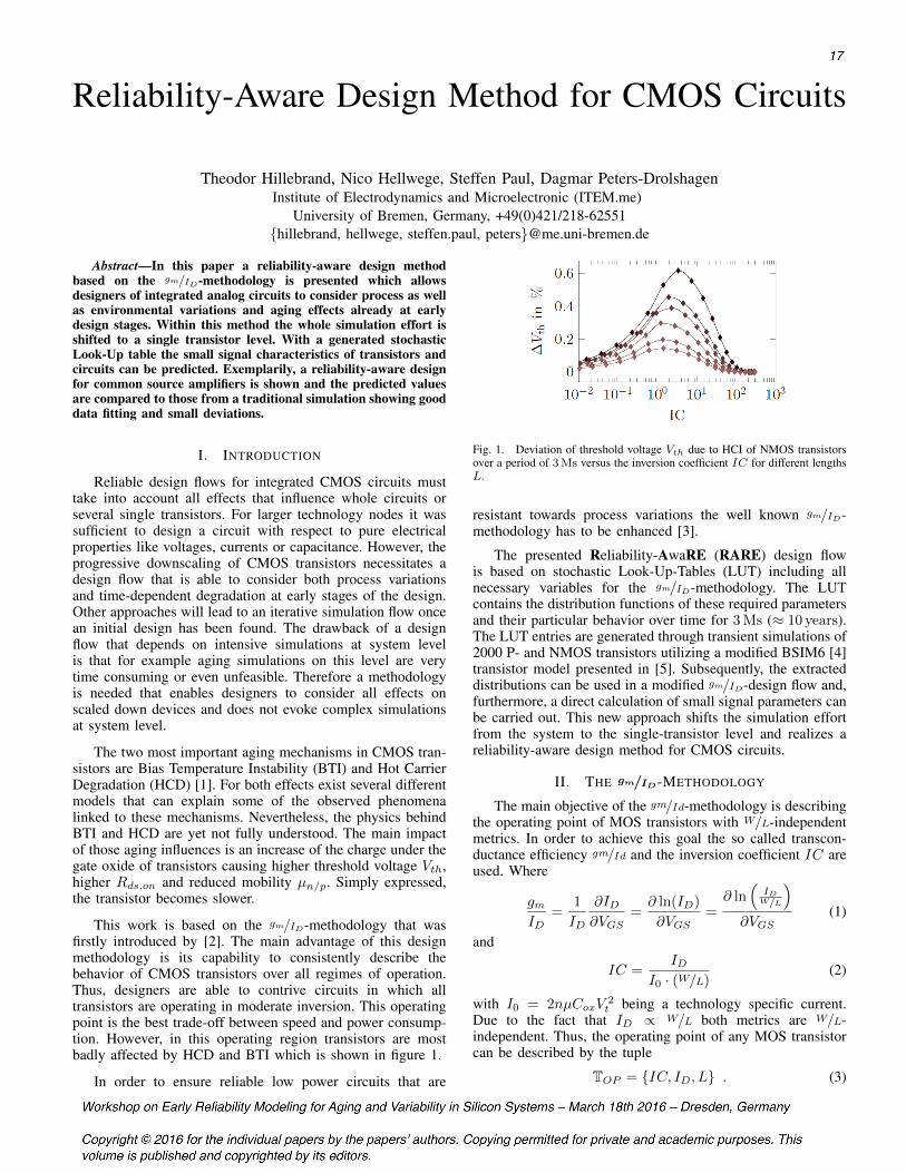
-methodology that wasfirstly introduced by [2]. The main advantage of this designmethodology is its capability to consistently describe thebehavior of CMOS transistors over all regimes of operation.Thus, designers are able to contrive circuits in which alltransistors are operating in moderate inversion. This operatingpoint is the best trade-off between speed and power consump-tion. However, in this operating region transistors are mostbadly affected by HCD and BTI which is shown in figure 1.
In order to ensure reliable low power circuits that are
Fig. 1. Deviation of threshold voltage Vth due to HCI of NMOS transistorsover a period of 3Ms versus the inversion coefficient IC for different lengthsL.
resistant towards process variations the well known gm
/ID
-methodology has to be enhanced [3].
The presented Reliability-AwaRE (RARE) design flowis based on stochastic Look-Up-Tables (LUT) including allnecessary variables for the g
m
/ID
-methodology. The LUTcontains the distribution functions of these required parametersand their particular behavior over time for 3Ms (⇡ 10 years).The LUT entries are generated through transient simulations of2000 P- and NMOS transistors utilizing a modified BSIM6 [4]transistor model presented in [5]. Subsequently, the extracteddistributions can be used in a modified g
m
/ID
-design flow and,furthermore, a direct calculation of small signal parameters canbe carried out. This new approach shifts the simulation effortfrom the system to the single-transistor level and realizes areliability-aware design method for CMOS circuits.
II. THE gm/ID-METHODOLOGY
The main objective of the gm/Id-methodology is describing
the operating point of MOS transistors with W/L-independent
metrics. In order to achieve this goal the so called transcon-ductance efficiency gm
/Id and the inversion coefficient IC areused. Where
gm
ID=
1
ID
@ID
@VGS=
@ ln(ID)
@VGS=
@ ln
⇣ID
W/L
⌘
@VGS(1)
and
IC =
ID
I
0
· (W/L)(2)
with I
0
= 2nµCoxV2
t being a technology specific current.Due to the fact that ID / W
/L both metrics are W/L-
independent. Thus, the operating point of any MOS transistorcan be described by the tuple
TOP = {IC, ID, L} . (3)
By choosing an operating point, e.g. in moderate inversion, theIC is set, which leads to ID, further L should be chosen largeenough to prevent short channel effects. According to equation(2) the width can be calculated as
W =
ID · LI
0
· IC . (4)
To improve the accuracy of this method Look-up tables areused because the simulated data considers additional effectswhich may be included in specific transistor models andmanufacturing processes. The transconductance is then derivedfrom
gm =
✓gm
ID
◆
sim· ID . (5)
Utilizing this design method the operating point of everytransistor in a circuit can be derived and furthermore smallsignal performances of the circuit can be directly analyzed.
III. GENERATION OF STOCHASTIC LUTS
Due to the fact that within the mentioned gm/Id-
methodology every transistor is designed separately, it issufficient for the LUT to analyze the behavior of one PMOSand one NMOS transistor. The only parameters that have tobe swept, are the length L and the gate-source voltage Vgs.
Lmin L 3⇥ Lmin
0 Vgs Vdd = 1V (6)
Within this work a 65 nm CMOS technology is consideredthe maximum length of which is confined to 3 ⇥ Lmin. Forevery specific sweep point a 3Ms transient simulation with2000 transistors affected by process and temperature variationis performed. Table I shows the normal distribution functionsof all considered parameters with their particular mean valueµ and standard deviation �. The values for µ and � correspondto those which are specified by the technology.
TABLE I. PARAMETERS OF NORMAL DISTRIBUTION FUNCTIONS OFALL CONSIDERED QUANTITIES
Parameter Symbol µ �
Temperature T 27
�C
p2
�C
Gate oxide thickness tox
tox,norm
7pm
Length L Lspec
2nm
Width W Wspec
2nm
Gate doping concentration Ngate
Ngate,norm
5 · 1022 m�3
Channel doping concentration Ndep
Ndep,norm
1 · 1021 m�3
Source / Drain doping concentration NS/D
NS/D,norm
1 · 1023 m�3
Figure 2 shows the test benches for NMOS and PMOStransistors.
Fig. 2. Test benches for NMOS (a) and PMOS (b) transistors.
The simulation data is fitted either with a normal fn(x, t)(7) or with a log-normal fln(x, t) (8) distribution depending onwhich one describes the basic population best. Two differentdistribution functions are required because some distributionfunctions are symmetrical and some possibly not.
fn(x, t) =1p2⇡�
exp
�1
2
✓x� µ
�
◆2
!(7)
fln(x, t) =
8<
:1p
2⇡�xexp
✓� 1
2
⇣ln (x)�µ
�
⌘2
◆x > 0
0 x 0
(8)
x denotes any fitted parameter (e.g. IC, gm) and t is the time.These two functions were chosen because both have two fittingparameters (µ, �) with the same meaning and this simplifiesthe calculus of small signal parameters. The time dependencycomes in with the fitting of µ and �, as a matter of simplicity,with a fourth order polynomial function over time which gives
µ(t) = p
1,µt4
+ p
2,µt3
+ p
3,µt2
+ p
4,µt+ p
5,µ (9)
and
�(t) = p
1,�t4
+ p
2,�t3
+ p
3,�t2
+ p
4,�t+ p
5,� . (10)
The numerical analysis is performed in MATLAB. The sim-ulation data is reduced from 16 GB to approximately 240 MBcontaining the same amount of information. The data reductioncan be realized by storing the coefficient of distribution andfitting functions instead of storing the whole data. The secondadvantage is that this simulation has to be performed only oncefor every technology. Moreover, the resulting time-dependentdistribution functions for the parameters can subsequently beused in the gm
/Id-methodology which is shown in the nextsection.
IV. CALCULATION OF SMALL SIGNAL PARAMETERS
In order to perform the calculation of small signal parame-ters for MOS transistors as well as circuit performances like theDC gain ADC of common source amplifiers, some calculationspecification has to be performed in a different manner becauserandom variables are considered. The inversion coefficient ICis given by equation (2) where I
D
, I0
, W and L are partiallyindependent random variables denoted with bold print. Animportant fact is that some parameters are not stochasticallyindependent, thus the covariance is
cov(x,y) 6= 0 . (11)
In common design flows the technology current I0
is treatedas a constant value for each technology. However, in this casethis current is given by I
0
= 2nµCox
V
t
2 which is not aconstant value because each parameter is affected in a differentway by the variations specified in table I. Table II showsthe interdependencies of I
0
and the process/environmentalvariations.
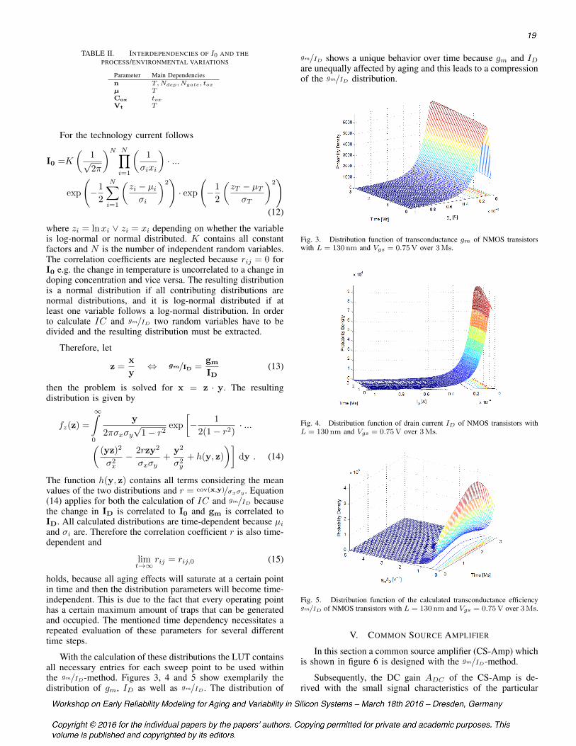
TABLE II. INTERDEPENDENCIES OF I0 AND THEPROCESS/ENVIRONMENTAL VARIATIONS
Parameter Main Dependenciesn T,N
dep
, Ngate
, tox
µ TC
ox
tox
V
t
T
For the technology current follows
I
0
=K
✓1p2⇡
◆N NY
i=1
✓1
�ixi
◆· ...
exp
�1
2
NX
i=1
✓zi � µi
�i
◆2
!· exp
�1
2
✓zT � µT
�T
◆2
!
(12)
where zi = lnxi _ zi = xi depending on whether the variableis log-normal or normal distributed. K contains all constantfactors and N is the number of independent random variables.The correlation coefficients are neglected because rij = 0 forI
0
e.g. the change in temperature is uncorrelated to a change indoping concentration and vice versa. The resulting distributionis a normal distribution if all contributing distributions arenormal distributions, and it is log-normal distributed if atleast one variable follows a log-normal distribution. In orderto calculate IC and g
m
/ID
two random variables have to bedivided and the resulting distribution must be extracted.
Therefore, let
z =
x
y
, gm/I
D
=
g
m
I
D
(13)
then the problem is solved for x = z · y. The resultingdistribution is given by
fz(z) =
1Z
0
y
2⇡�x�y
p1� r
2
exp
� 1
2(1� r
2
)
· ...
✓(yz)
2
�
2
x
� 2rzy
2
�x�y+
y
2
�
2
y
+ h(y, z)
◆�dy . (14)
The function h(y, z) contains all terms considering the meanvalues of the two distributions and r =
cov(x,y)/�
x
�y
. Equation(14) applies for both the calculation of IC and g
m
/ID
becausethe change in I
D
is correlated to I
0
and g
m
is correlated toI
D
. All calculated distributions are time-dependent because µi
and �i are. Therefore the correlation coefficient r is also time-dependent and
lim
t!1rij = rij,0 (15)
holds, because all aging effects will saturate at a certain pointin time and then the distribution parameters will become time-independent. This is due to the fact that every operating pointhas a certain maximum amount of traps that can be generatedand occupied. The mentioned time dependency necessitates arepeated evaluation of these parameters for several differenttime steps.
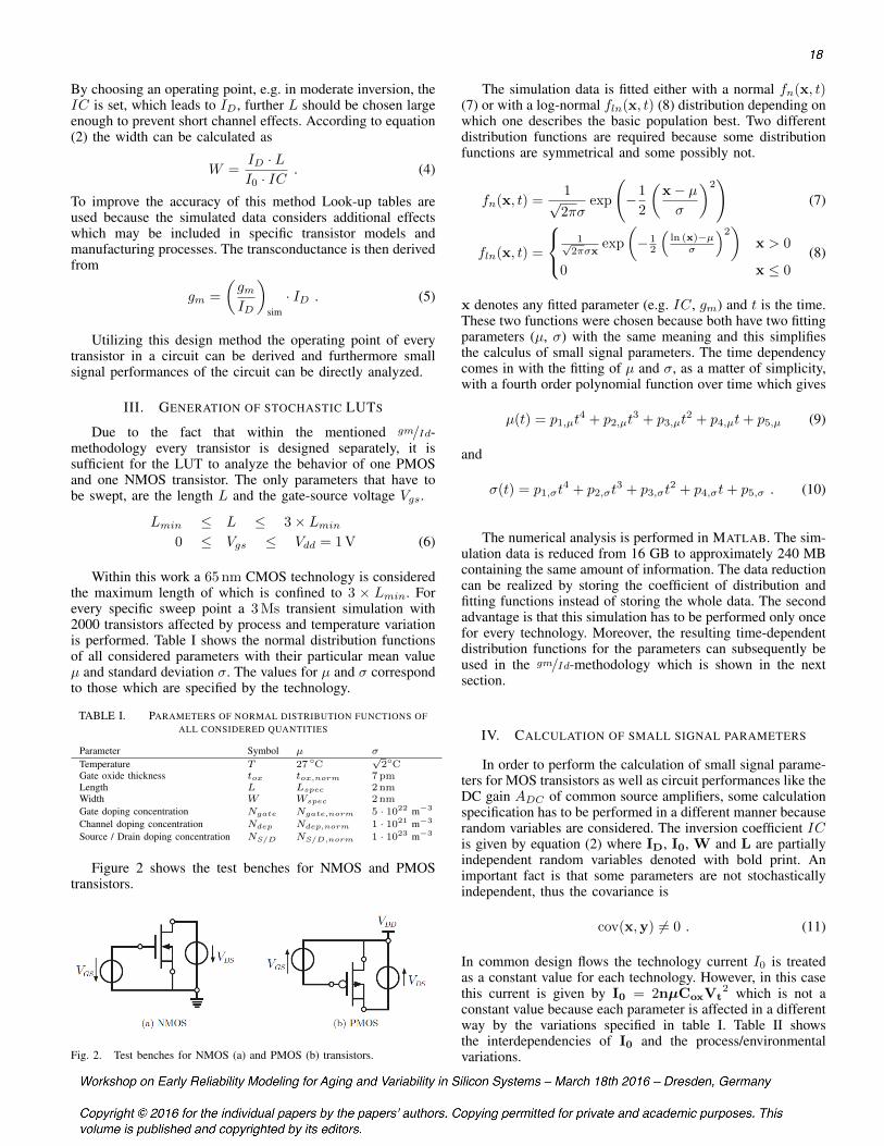
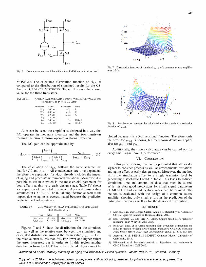
With the calculation of these distributions the LUT containsall necessary entries for each sweep point to be used withinthe g
m
/ID
-method. Figures 3, 4 and 5 show exemplarily thedistribution of gm, ID as well as g
m
/ID
. The distribution of
gm
/ID
shows a unique behavior over time because gm and ID
are unequally affected by aging and this leads to a compressionof the g
m
/ID
distribution.
Fig. 3. Distribution function of transconductance gm of NMOS transistorswith L = 130 nm and Vgs = 0.75V over 3Ms.
Fig. 4. Distribution function of drain current ID of NMOS transistors withL = 130 nm and Vgs = 0.75V over 3Ms.
Fig. 5. Distribution function of the calculated transconductance efficiencygm/I
D
of NMOS transistors with L = 130 nm and Vgs = 0.75V over 3Ms.
V. COMMON SOURCE AMPLIFIER
In this section a common source amplifier (CS-Amp) whichis shown in figure 6 is designed with the g
m
/ID
-method.
Subsequently, the DC gain ADC of the CS-Amp is de-rived with the small signal characteristics of the particular
M3 M2
VDD VDD
Vout
Ibias
VSSVin
VSS
M1
Fig. 6. Common source amplifier with active PMOS current mirror load.
MOSFETs. The calculated distribution function of ADC iscompared to the distribution of simulated results for the CS-Amp in CADENCE VIRTUOSO. Table III shows the chosenvalue for the three transistors.
TABLE III. APPROPRIATE OPERATING POINT PARAMETER VALUES FORTRANSISTORS IN THE CS-AMP
Parameter Value Parameter ValueW1 260nm IC1 5W2 260nm IC2 50W3 2.6 µm IC3 50L1 130nm
L2 130nm ID
100 µAL3 130nm I0 995nA
As it can be seen, the amplifier is designed in a way thatM1 operates in moderate inversion and the two transistorsforming the current mirror operate in strong inversion.
The DC gain can be approximated by
ADC =
⇣g
m,1
I
D
⌘
sim⇣g
ds,1
I
D
⌘
sim+
⇣g
ds,2
I
D
⌘
sim
=
g
m,1
g
ds,1 + g
ds
2
. (16)
The calculation of ADC follows the same scheme likethat for IC and g
m
/ID
. All conductances are time-dependent,therefore the expression for ADC already includes the impactof aging and process/environmental variations. Moreover, it ispossible to evaluate which is the most crucial parameter forboth effects at this very early design stage. Table IV showsa comparison of predicted fresh/aged ADC and those valuessimulated in CADENCE. The initial amplification as well as theimpact due to aging is overestimated because the predictionneglects the load resistance.
TABLE IV. COMPARISON OF MEAN PREDICTED AND SIMULATEDFRESH/AGED ADC .
Fresh Value Aged ValueA
DC,pre
93.1dB ADC,pre
13.7dBA
DC,sim
82.3dB ADC,sim
19.12dB
Figures 7 and 8 show the distribution for the simulatedgm,1 as well as the relative error between the simulated andcalculated distribution. Around the mean value µg
m,1 = 1mS
the relative error is less than 3%. For lower and higher valuesthe error increases, but in order to fit this region anotherdistribution from the LUT has to be utilized. ADC cannot be
Fig. 7. Distribution function of simulated gm,1 of a common source amplifierover 3Ms.
Fig. 8. Relative error between the calculated and the simulated distributionfunction of gm,1.
plotted because it is a 5-dimensional function. Therefore, onlythe error for gm,1 is shown, but the shown deviation appliesalso for gds,1 and gds,2.
Additionally, the shown calculation can be carried out forevery small signal circuit performance.
VI. CONCLUSION
In this paper a design method is presented that allows de-signers to consider process as well as environmental variationsand aging effect at early design stages. Moreover, the methodshifts the simulation effort to a single transistor level bygenerating a stochastic Look-Up Table. This leads to reducedsimulation time and amount of data that must be stored.With this data good predictions for small signal parametersof MOSFET and circuit performances can be derived. Themethod is evaluated with the design of a common sourceamplifier showing only small errors in the prediction of theinitial distribution as well as for the degraded distribution.
REFERENCES
[1] Maricau, Elie, and Georges Gielen. Analog IC Reliability in NanometerCMOS. Springer Science & Business Media, 2013.
[2] Enz, Christian C., and Eric A. Vittoz. Charge-based MOS transistormodeling. John Wiley & Sons, 2006.
[3] Hellwege, Nico, et al. Using operating point-dependent degradation andg m/I D method for aging-aware design. Integrated Reliability Workshop
Final Report (IRW), 2013 IEEE International. IEEE, 2013. S. 113-116.[4] Agarwal, et al. BSIM6.1.0 MOSFET Compact Model. University of
Calirfornia, 2014.[5] Hillebrand, et al. Stochastic analysis of degradation and variations in
CMOS Transistors, ZuE 2015.


![Cmos Rf Cituits Sic] Variability And Reliability Resilient](https://img.pdfslide.net/doc/110x75/61eff30f1f58b06c3f317164/cmos-rf-cituits-sic-variability-and-reliability-resilient-.jpg)