Embed Size (px)
Citation preview

1
Supplementary Material
Reliability Improvement of a Flexible FD-SOI
MOSFET via Heat Management
Jae Hoon Bong1, Seung-Yoon Kim1, Chan Bae Jeong2, Ki Soo Chang2, Wan Sik Hwang3 and
Byung Jin Cho1,a)
1School of Electrical Engineering, Korea Advanced Institute of Science and Technology,
Daejeon, 34141, Republic of Korea 2Division of Scientific Instrumentation, Korea Basic Science Institute, Daejeon, 34133, Republic
of Korea 3Department of Materials Engineering, Korea Aerospace University, Goyang, 10540, Republic
of Korea
a) Corresponding author. E-mail: [email protected]
2
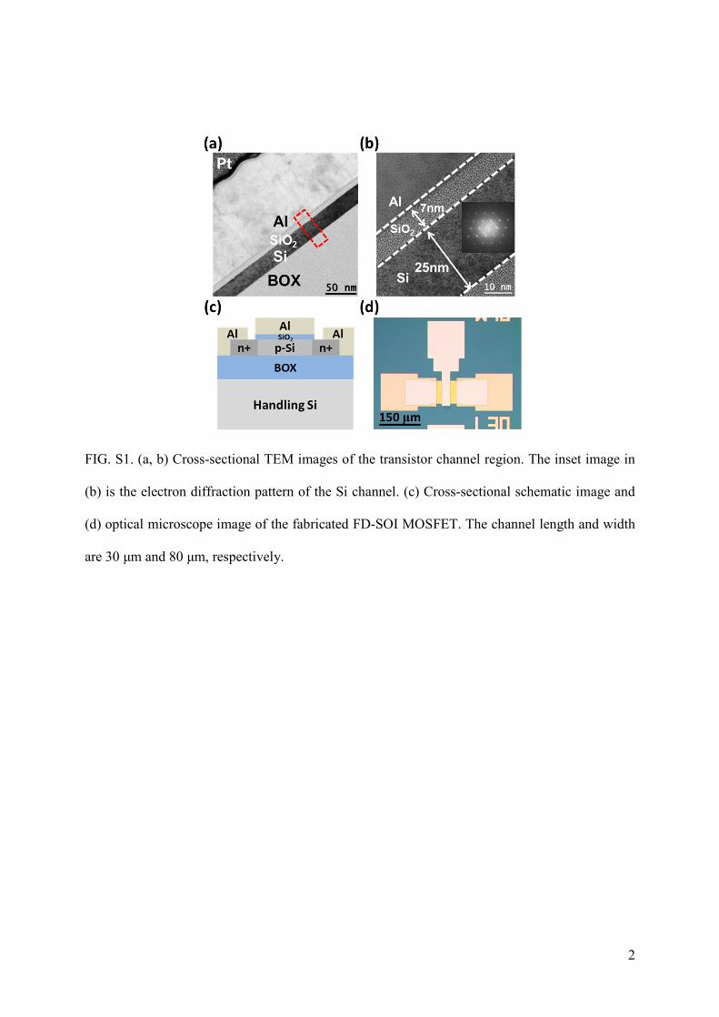
FIG. S1. (a, b) Cross-sectional TEM images of the transistor channel region. The inset image in
(b) is the electron diffraction pattern of the Si channel. (c) Cross-sectional schematic image and
(d) optical microscope image of the fabricated FD-SOI MOSFET. The channel length and width
are 30 μm and 80 μm, respectively.

3
FIG. S2. Drain currents of the sc-Si membrane transistor on PDMS/PI film with and without the
HSL as a function of bias stress time at VG = 3 V, VD = 8 V for 30 min.
FIG. S3. Repeated measurement results (ID-VG) of the bias-stressed sc-Si membrane transistor on
PDMS/PI film without the HSL.
0 5 10 15 20 25 300.5
1.0
1.5
2.0
2.5L/W(mm) = 30/80
w/ HSL w/o HSL
Drai
n cu
rrent
(mA)
Time (min)
VG = 3 V, VD = 8 V

4
FIG. S4. Maximum device temperature of the sc-Si membrane transistor on PDMS/PI film
without the silver HSL during the device operation at VG = 3 V, VD = 8 V.
FIG. S5. Large scale temperature profile image of the transferred Si membrane device w/o HSL.
The transistor inside box #6 is biased at VG = 3 V, VD = 8 V, and the other transistors are not
biased.
0 5 10 15 20 25 3020
30
40
50
60
70
80VG= 3 V, VD= 8 V
Time (min)
Tem
pera
ture
(°C)
5
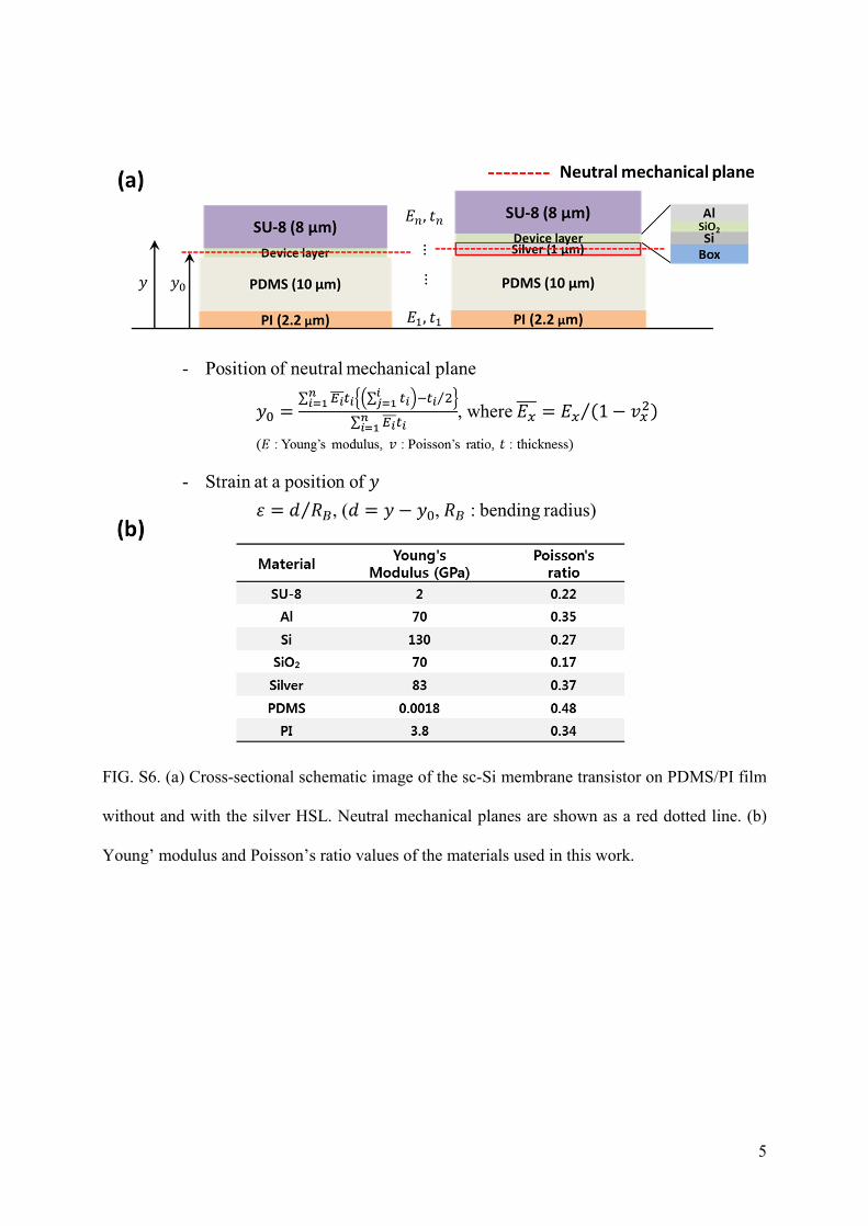
FIG. S6. (a) Cross-sectional schematic image of the sc-Si membrane transistor on PDMS/PI film
without and with the silver HSL. Neutral mechanical planes are shown as a red dotted line. (b)
Young’ modulus and Poisson’s ratio values of the materials used in this work.