Embed Size (px)
Citation preview
1
REMOTE CONTROL SOLAR PLOUGHING MACHINE
PROJECT REPORT
Submitted to
The Director/M.S (PCS&T)
REF No.10761/PCS&T/FA/PROJ/JSA-II/2014/648
GOVERNMENT OF PUDUCHERRY
DEPARTMENT OF SCIENCE, TECHNOLOGY AND ENVIRONMENT
PUDUCHERRU COUNCIL FOR SCIENCE AND TECHNOLOGY
III FLOOR,PHB BUILDING,ANNA NAGAR,PUDUCHERRY-5
2
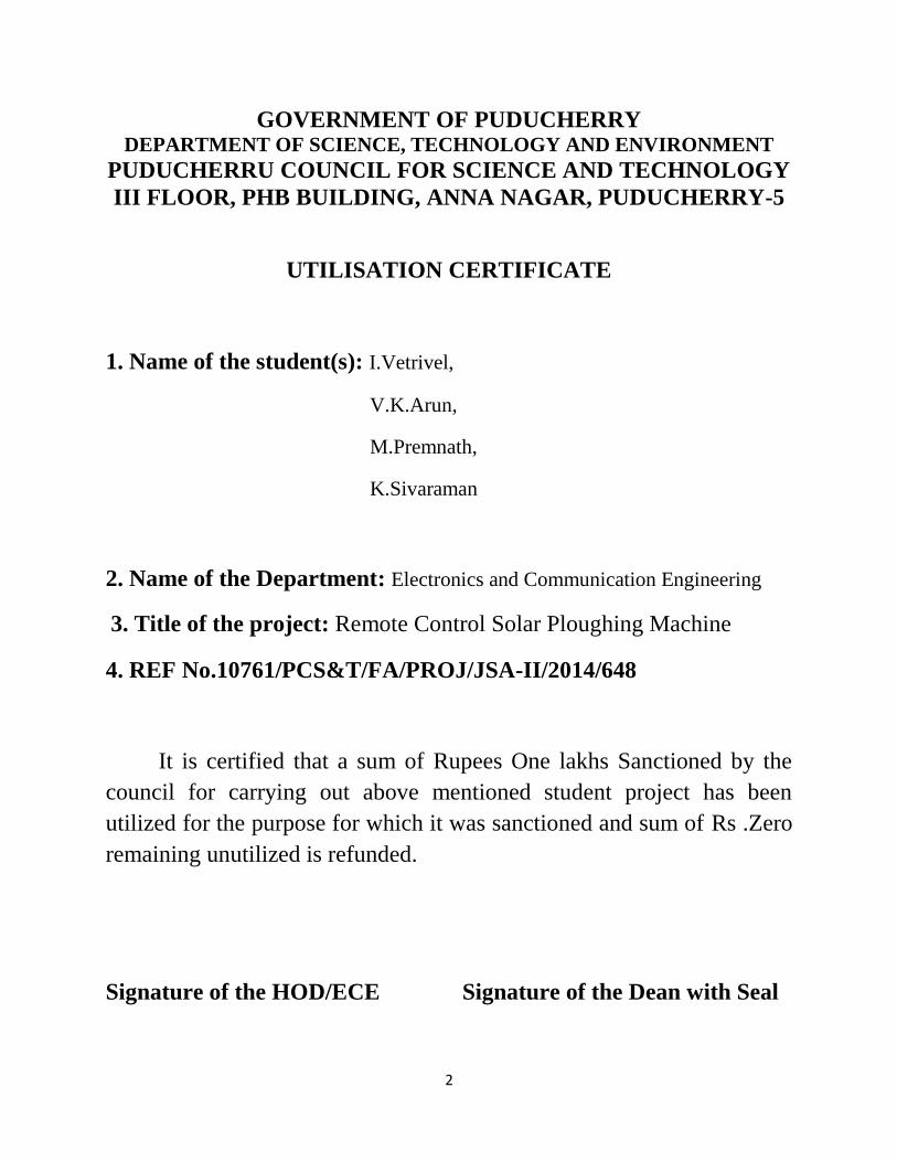
GOVERNMENT OF PUDUCHERRY DEPARTMENT OF SCIENCE, TECHNOLOGY AND ENVIRONMENT
PUDUCHERRU COUNCIL FOR SCIENCE AND TECHNOLOGY
III FLOOR, PHB BUILDING, ANNA NAGAR, PUDUCHERRY-5
UTILISATION CERTIFICATE
1. Name of the student(s): I.Vetrivel,
V.K.Arun,
M.Premnath,
K.Sivaraman
2. Name of the Department: Electronics and Communication Engineering
3. Title of the project: Remote Control Solar Ploughing Machine
4. REF No.10761/PCS&T/FA/PROJ/JSA-II/2014/648
It is certified that a sum of Rupees One lakhs Sanctioned by the
council for carrying out above mentioned student project has been
utilized for the purpose for which it was sanctioned and sum of Rs .Zero
remaining unutilized is refunded.
Signature of the HOD/ECE Signature of the Dean with Seal
3
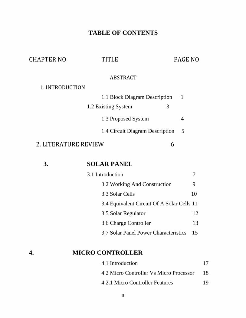
TABLE OF CONTENTS
CHAPTER NO TITLE PAGE NO
ABSTRACT
1. INTRODUCTION
1.1 Block Diagram Description 1
1.2 Existing System 3
1.3 Proposed System 4
1.4 Circuit Diagram Description 5
2. LITERATURE REVIEW 6
3. SOLAR PANEL
3.1 Introduction 7
3.2 Working And Construction 9
3.3 Solar Cells 10
3.4 Equivalent Circuit Of A Solar Cells 11
3.5 Solar Regulator 12
3.6 Charge Controller 13
3.7 Solar Panel Power Characteristics 15
4. MICRO CONTROLLER
4.1 Introduction 17
4.2 Micro Controller Vs Micro Processor 18
4.2.1 Micro Controller Features 19
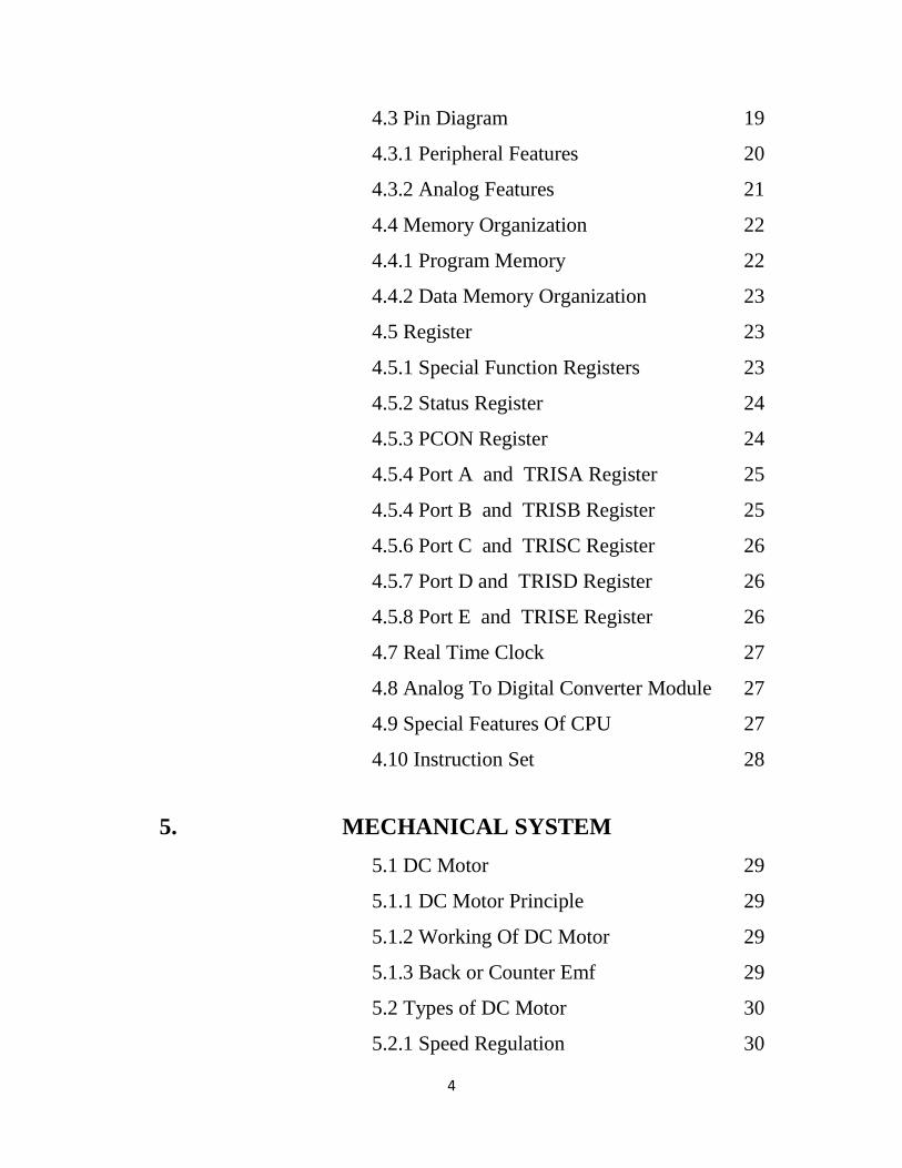
4
4.3 Pin Diagram 19
4.3.1 Peripheral Features 20
4.3.2 Analog Features 21
4.4 Memory Organization 22
4.4.1 Program Memory 22
4.4.2 Data Memory Organization 23
4.5 Register 23
4.5.1 Special Function Registers 23
4.5.2 Status Register 24
4.5.3 PCON Register 24
4.5.4 Port A and TRISA Register 25
4.5.4 Port B and TRISB Register 25
4.5.6 Port C and TRISC Register 26
4.5.7 Port D and TRISD Register 26
4.5.8 Port E and TRISE Register 26
4.7 Real Time Clock 27
4.8 Analog To Digital Converter Module 27
4.9 Special Features Of CPU 27
4.10 Instruction Set 28
5. MECHANICAL SYSTEM
5.1 DC Motor 29
5.1.1 DC Motor Principle 29
5.1.2 Working Of DC Motor 29
5.1.3 Back or Counter Emf 29
5.2 Types of DC Motor 30
5.2.1 Speed Regulation 30
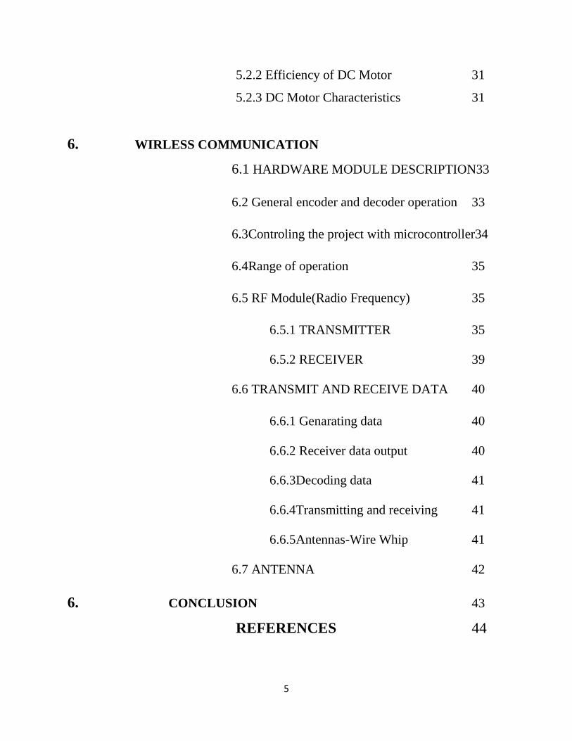
5
5.2.2 Efficiency of DC Motor 31
5.2.3 DC Motor Characteristics 31
6. WIRLESS COMMUNICATION
6.1 HARDWARE MODULE DESCRIPTION33
6.2 General encoder and decoder operation 33
6.3Controling the project with microcontroller34
6.4Range of operation 35
6.5 RF Module(Radio Frequency) 35
6.5.1 TRANSMITTER 35
6.5.2 RECEIVER 39
6.6 TRANSMIT AND RECEIVE DATA 40
6.6.1 Genarating data 40
6.6.2 Receiver data output 40
6.6.3Decoding data 41
6.6.4Transmitting and receiving 41
6.6.5Antennas-Wire Whip 41
6.7 ANTENNA 42
6. CONCLUSION 43
REFERENCES 44
6
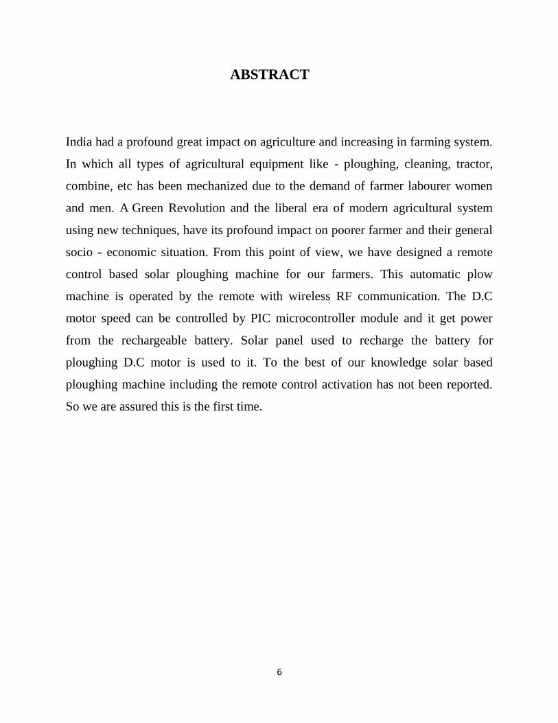
ABSTRACT
India had a profound great impact on agriculture and increasing in farming system.
In which all types of agricultural equipment like - ploughing, cleaning, tractor,
combine, etc has been mechanized due to the demand of farmer labourer women
and men. A Green Revolution and the liberal era of modern agricultural system
using new techniques, have its profound impact on poorer farmer and their general
socio - economic situation. From this point of view, we have designed a remote
control based solar ploughing machine for our farmers. This automatic plow
machine is operated by the remote with wireless RF communication. The D.C
motor speed can be controlled by PIC microcontroller module and it get power
from the rechargeable battery. Solar panel used to recharge the battery for
ploughing D.C motor is used to it. To the best of our knowledge solar based
ploughing machine including the remote control activation has not been reported.
So we are assured this is the first time.

7
CHAPTER-1 INTRODUCTION
1.1 DESCRIPTION
We are doing our project REMOTE CONTROL BASED SOLAR
PLOUGHING MACHINE. It is used to avoid the environmental pollution and
utilize the man power.
Our aim is manufacture the plow machine and everyone to operate it especially the
youth to take part in the agriculture.
In future we proposed all the tillage tolls are placed in our remote control machine.
One of the major economic issues faced by the country is agriculture as this is the
sector which is source of livelihood for about 54% of Indians till date. Still today
this sector is not well developed and faces lots of problems resulting into low
productivity of crops.
Indian agriculture includes a mix of traditional to modern farming techniques. In
some parts of India, traditional use of cattle to plough farms remains in use.
Traditional farms have some of the lowest per capita productivities and farmer
incomes.
Since 2002, India has become the world's largest manufacturer of tractorswith 29%
of world's output in 2013; it is also the world's largest tractor market. Above a
tractor in use in north India.
The main advantage of the project is avoid the environmental pollution from
an exhaust gas and utilizes the renewable source. And it‟s easy to handle
8
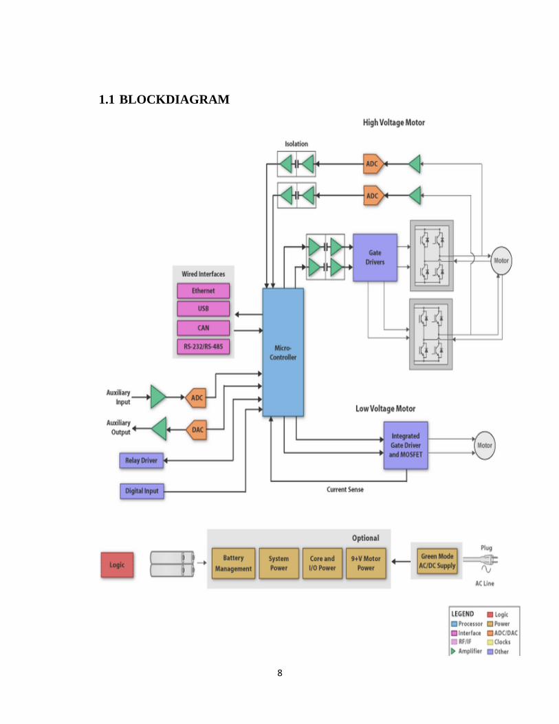
1.1 BLOCKDIAGRAM
9
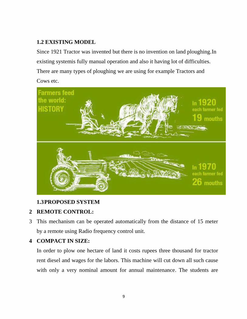
1.2 EXISTING MODEL
Since 1921 Tractor was invented but there is no invention on land ploughing.In
existing systemis fully manual operation and also it having lot of difficulties.
There are many types of ploughing we are using for example Tractors and
Cows etc.
1.3 PROPOSED SYSTEM
2 REMOTE CONTROL:
3 This mechanism can be operated automatically from the distance of 15 meter
by a remote using Radio frequency control unit.
4 COMPACT IN SIZE:
In order to plow one hectare of land it costs rupees three thousand for tractor
rent diesel and wages for the labors. This machine will cut down all such cause
with only a very nominal amount for annual maintenance. The students are
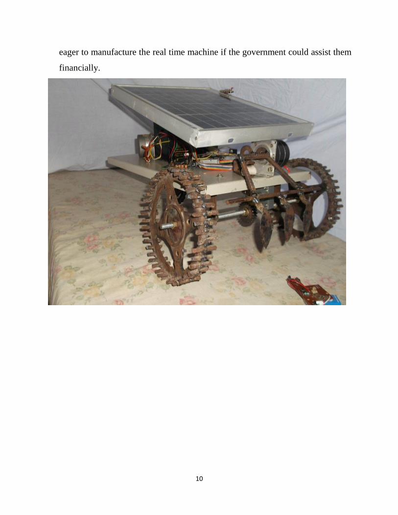
10
eager to manufacture the real time machine if the government could assist them
financially.
11
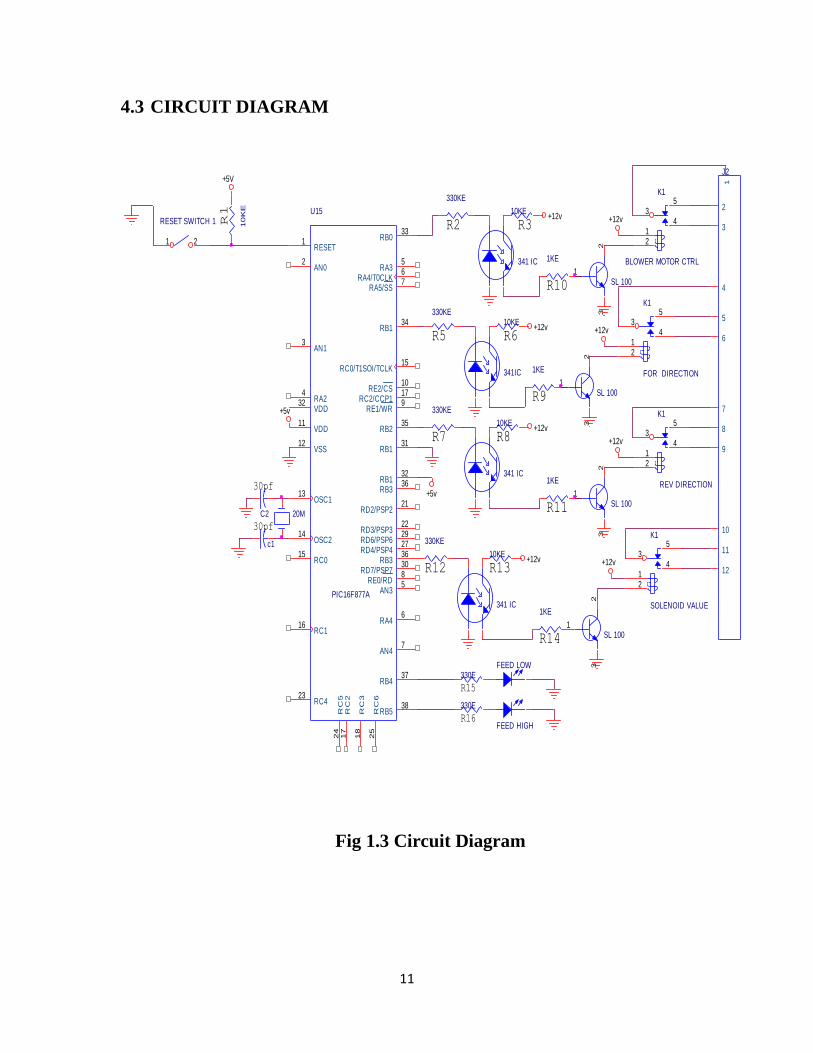
4.3 CIRCUIT DIAGRAM
Fig 1.3 Circuit Diagram
+5v
SL 1001
23
1KE
R6
1KE
30pf
341 IC
+12vR3
U15
PIC16F877A
2
3
4
567
33
34
35
36
5
6
7
37
15
15
17
16
23
24
17
18
32
1
13
14
11
8
9
10
38
25
21
22
2736
29
30
12 31
32
AN0
AN1
RA2
RA3RA4/T0CLK
RA5/SS
RB0
RB1
RB2
RB3
AN3
RA4
AN4
RB4
RC0/T1SOI/TCLK
RC0
RC2/CCP1
RC1
RC4
RC
5R
C2
RC
3
VDD
RESET
OSC1
OSC2
VDD
RE0/RD
RE1/WR
RE2/CS
RB5RC
6
RD2/PSP2
RD3/PSP3
RD4/PSP4RB3
RD6/PSP6
RD7/PSP7
VSS RB1
RB1
R10
330KE
+5v
FEED HIGH
30pf
341IC
+12v10KE
R9
330E
+12v
1KE
+12vR8
c1
+12v
341 IC
10KE
R7
+12v
SL 1001
23
R11
+12v
330KE
10K
E
341 IC
330KE
+12v
R15
SL 1001
23
K1
REV DIRECTION
35
412
R1
20M
SL 1001
23
K1
SOLENOID VALUE
35
412
R16
10KE
+5V
RESET SWITCH 1
1 2
10KE
R12
K1
BLOWER MOTOR CTRL
35
412
C2
R14
330E
K1
FOR DIRECTION
35
412
FEED LOW
R13
J2
1
2
3
4
5
7
8
9
6
10
11
12
R2
330KE
R5
1KE
12
CHAPTER 2
LITERATURE SURVEY
1. Ludwig Kronthaler,EURAC Research,Institute for Renewable Energy,Viale
Druso 1,39100 Bolzano, Italy. This paper presents a screening methodology
to evaluate the economic feasibility and environmental impact of Vehicle-
integrated Photovoltaic (ViPV) Systems by means of various indicators.
2. Selver Senturk Turkish Agricultural Monitoring & Information Center
Istanbul Technical University Maslak, Istanbul For structuring national
irrigation policies and determining the exact yield production shares
separately generated from irrigated and unirrigated farmland practices fast
and simple to employ methods are of great importance. In this work, through
utilizing entire satellite image frames, with no masking or cropping any parts
out, a local, parcel-based Normalized Difference Vegetation Index (NDVI)
and Normalized Difference Moisture Index (NDMI) means and variance
techniques‟ mapping abilities were investigated.
13
CHAPTER 3
SOLAR PANEL
3.1 INTRODUCTION
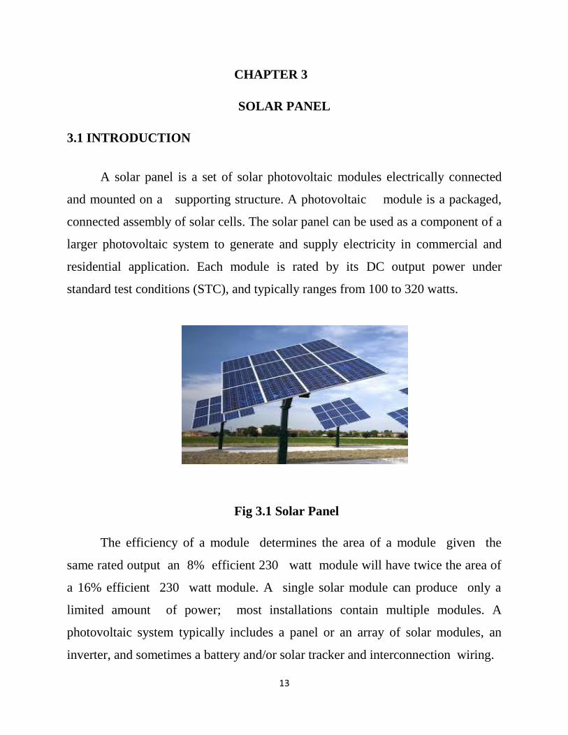
A solar panel is a set of solar photovoltaic modules electrically connected
and mounted on a supporting structure. A photovoltaic module is a packaged,
connected assembly of solar cells. The solar panel can be used as a component of a
larger photovoltaic system to generate and supply electricity in commercial and
residential application. Each module is rated by its DC output power under
standard test conditions (STC), and typically ranges from 100 to 320 watts.
Fig 3.1 Solar Panel
The efficiency of a module determines the area of a module given the
same rated output an 8% efficient 230 watt module will have twice the area of
a 16% efficient 230 watt module. A single solar module can produce only a
limited amount of power; most installations contain multiple modules. A
photovoltaic system typically includes a panel or an array of solar modules, an
inverter, and sometimes a battery and/or solar tracker and interconnection wiring.
14
3.2 WORKING AND CONSTRUCTIONS
Solar modules use light energy photons from the sun to generate electricity
through the photovoltaic effect. The majority of modules use wafer-based
crystalline silicon cells or thin film cells based on cadmium telluride or silicon.
The structural(load carrying)member of a module can either be the top layer or the
back layer. Cells must also be protected from mechanical damage and
moisture. Most solar
modules are rigid, but semi-flexible ones are available, based on thin-film
cells. These early solar modules were first used in space in 1958.
Electrical connections are made in series to achieve a desired output
voltage and/or in parallel to provide a desired current capability. The conducting
wire that take the current off the modules may contain silver, copper or other non-
magnetic conductive transition metals.

15
Fig 3.2 Solar Working
The cells must be connected electrically to one another and to the rest of the
system .Externally popular terrestrial usage photovoltaic modules use MC3 (older)
or MC4 connectors to facilitate easy weatherproof connections to the rest of the
system.
Bypass diodes may be incorporated or used externally, in case of partial
module shading, to maximize the output of module sections still illuminated.
Some recent solar module designs include concentrators in which light is
focused by lenses or mirrors onto an array of smaller cells. This enables the use of
cells with a high cost per unit area (such as gallium arsenide) in a cost
effective way.

16
3.3 SOLAR CELL
A solar cell made from a mono crystalline siliconwafer with its contact
grid made from bus bars (the larger strips) and fingers (the smaller ones)Solar cells
can be used in devices such as this portable mono crystalline solar charger. A solar
cell(also called a photovoltaic cell)is an electrical device that converts the energy
of light directly into electricity by the photovoltaic effect.
It is a form of photoelectric cell (in that its electrical characteristics e.g.
current, voltage, or resistance vary when light is incident upon it) which, when
exposed to light, can generate and support an electric current without being
attached to any external voltage source, but do require an external load for power
consumption.
The term "photovoltaic" comes from the Greek meaning "light", and from
"volt", the unit of electro-motive force, the volt, which in turn comes from the last
name of the Italian physicist Alessandro Volta, inventor of the battery
(electrochemical cell). The term "photo-voltaic" has been in use in English since
1849.
Photovoltaicis the field of technology and research related to the practical
application of photovoltaic cells in producing electricity from light, though it is
often used specifically to refer to the generation of electricity from sunlight. Cells
can be described as photovoltaic even when the light source is not necessarily
sunlight (lamplight, artificial light, etc.). In such cases the cell is sometimes used as
a photo detector (for example infrared detectors), detecting light or other
electromagnetic radiation near the visible range, or measuring light intensity.
17
A solar cell (also called a photovoltaic cell) is an electrical device that
converts the energy of light directly into electricity by the photovoltaic effect. It is
a form of photoelectric cell (in that its electrical characteristics e.g. current,
voltage, or resistance vary when light is incident upon it) which, when exposed to
light, can generate and support an electric current without being attached to any
external voltage source, but do require an external load for power consumption.
The term "photovoltaic" comes from the meaning "light", and from "volt",
the unit of electro-motive force, the volt, which in turn comes from the last name
of the Italian physicist Alessandro Volta, inventor of the battery (electrochemical
cell). The term "photo-voltaic" has been in use in English since 1849.
The operation of a photovoltaic (PV) cell requires 3 basic attributes:
1. The absorption of light, generating either electron-hole pairs or excitons.
2. The separation of charge carriers of opposite types.
3. The separate extraction of those carriers to an external circuit.
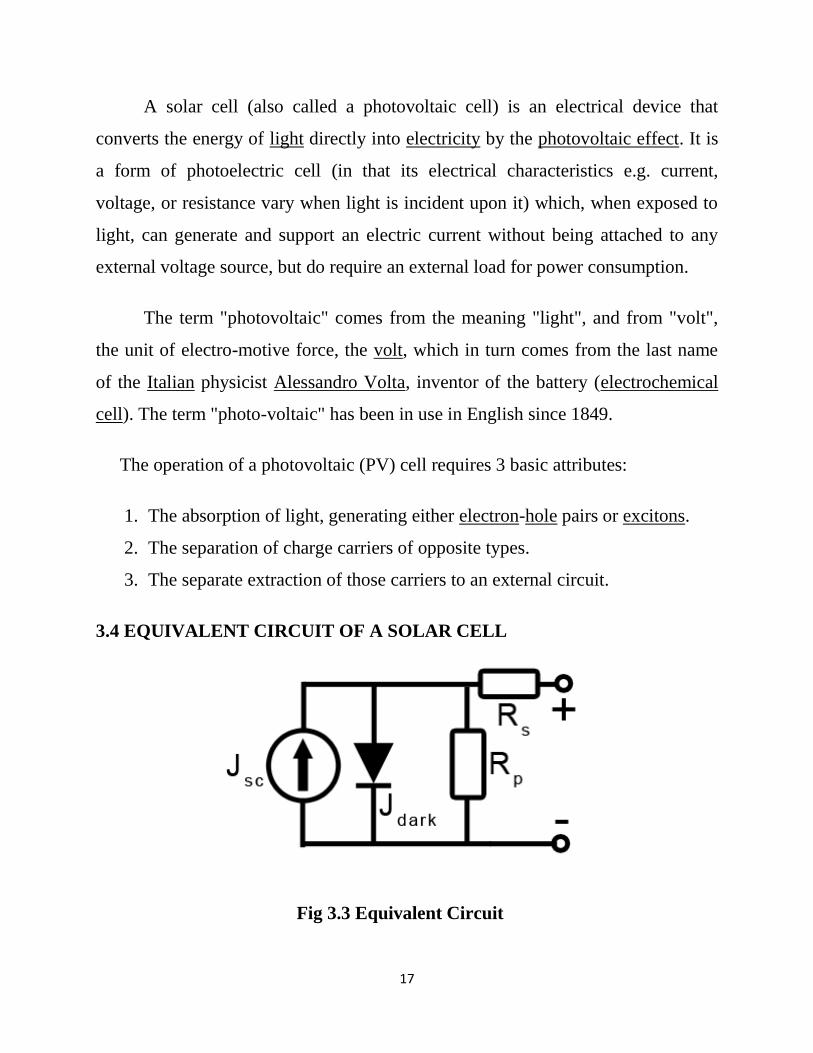
3.4 EQUIVALENT CIRCUIT OF A SOLAR CELL
Fig 3.3 Equivalent Circuit
18
The solar cell can be seen as a current generator which generates the current
(density) Jsc. The dark current flows in the opposite direction and is caused by a
potential between the + and - terminals. In addition you would have two
resistances; one in series (Rs) and one in parallel (Rp). The series resistance is
caused by the fact that a solar cell is not a perfect conductor. The parallel
resistance is caused by leakage of current from one terminal to the other due to
poor insulation, for example on the edges of the cell. In an ideal solar cell, you
would have Rs = 0 and Rp = ∞.
When these so called parasitic resistances are included, the current
expression (1.3) becomes
3.5 SOLAR REGULATOR
A solar regulator (also known as a charge controller) is used in conjunction
with a stand alone (off grid) system, or a grid connect solar power system that
incorporates a backup battery bank. For a grid connect solar power system that
doesn't use batteries, a solar regulator is not needed.
A solar regulator is a small box consisting of solid state circuitry that is
placed between a solar panel and a battery. Its function is to regulate the amount of
charge coming from the panel that flows into the deep cycle battery bank in order
to avoid the batteries being overcharged. A regulator can also provide a direct
connection to appliances, while continuing to recharge the battery; i.e. you can run
appliances directly from it, bypassing the battery bank; but the batteries will
continue to be charged.
19
3.6 CHARGE CONTROLLER
A charge controller, charge regulator or battery regulator limits the rate at
which electric current is added to or drawn from electric batteries. It prevents
overcharging and may prevent against overvoltage, which can reduce battery
performance or lifespan, and may pose a safety risk. It may also prevent
completely draining ("deep discharging") a battery, or perform controlled
discharges, depending on the battery technology, to protect battery life.
The terms "charge controller" or "charge regulator" may refer to either a
stand-alone device, or to control circuitry integrated within a battery pack, battery-
powered device, or battery recharger.
3.7 SOLAR PANEL POWER CHARACTERISTICS
The current and power output of photovoltaic solar panels are approximately
proportional to the sun‟s intensity. At a given intensity, a solar panel's output
current and operating voltage are determined by the characteristics of the load. If
that load is a battery, the battery's internal resistance will dictate the module's
operating voltage.
A solar panel, which is rated at 17 volts will put out less than its rated power
when used in a battery system. That‟s because the working voltage will be between
12 and 15 volts. Because wattage (or power) is the product of volts multiplied by
the amps, the module output will be reduced. For example, a 50-watt solar panel
working at 13.0 volts will products 39.0 watts (13.0 volts x 3.0 amps = 39.0 watts).
This is important to remember when sizing a PV system.
20
An I-V curve (see image on right) is simply all of a solar panel's possible
operating points (voltage/current combinations) at a given cell temperature and
light intensity. Increases in cell temperature increase a solar panel‟s current
slightly, but significantly decreases voltage and current.
Two important quantities to characterize a solar cell are
Open circuit voltage (Voc): The voltage between the terminals when no
current is drawn (infinte load resistance)
Short circuit current (Isc): The current when the terminals are connected to
eachother (zero load resistance)
The short circuit current increases with light intensity, as higher intensity means
more photons, which in turn means more electrons. Since the short circuit current
Isc is roughly proportional to the area of the solar cell, the short circuit current
density, Jsc = Isc/A, is often used to compare solar cells.
When a load is connected to the solar cell, the current decreases and a voltage
develops as charge builds up at the terminals. The resulting current can be viewed
as a superposition of the short circuit current, caused by the absorbtion of photons,
and a dark current, which is caused by the potential built up over the load and
flows in the opposite direction. As a solar cell contains a PN-junction (LINK), just
as a diode, it may be treated as a diode. For an ideal diode, the dark current density
is given by
(1.1)
21
Here J0 is a constant, q is the electron charge and V is the voltage between
the terminals. The resulting current can be approximated as a superposition of the
short circuit current and the dark current:
(1.2)
To find an expression for the open circuit voltage, Voc, we use (1.2) setting J
= 0. This means that the two currents cancel out so that no current flows, which
exactly is the case in an open circuit. The resulting expression is
(1.3)
3.8 EFFICIENCY
In general, the power delivered from a power source is P = IV, i.e. the
product of voltage and current. If we instead use the current density J, we get the
power density:
(1.4)
The maximum power density occurs somewhere between V = 0 (short
circuit) and V = Voc (open circuit) at a voltage Vm. The corresponding current
density is called Jm, and thus the maximum power density is Pd,m = JmVm.
The efficiency of a solar cell is defined as the power (density) output divided
by the power (density) output. If the incoming light has a power density Ps, the
efficiency will be
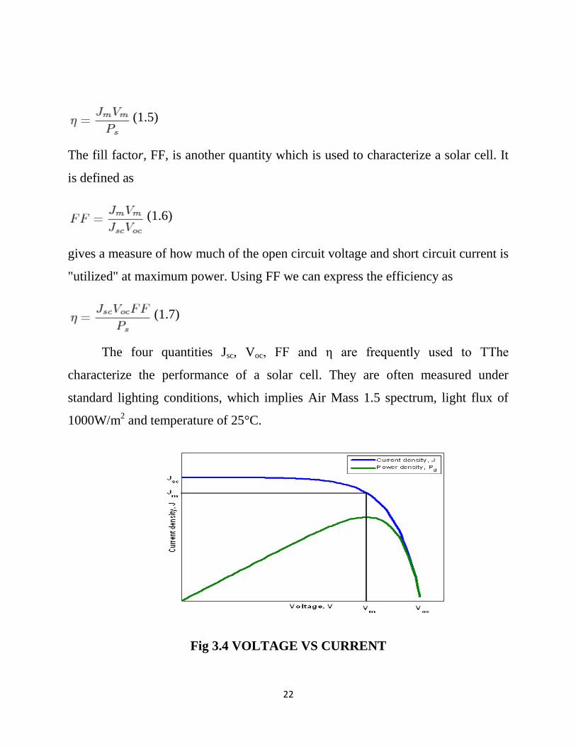
22
The fill factor, FF, is another quantity which is used to characterize a solar cell. It
is defined as
(1.6)
gives a measure of how much of the open circuit voltage and short circuit current is
"utilized" at maximum power. Using FF we can express the efficiency as
The four quantities Jsc, Voc, FF and η are frequently used to TThe
characterize the performance of a solar cell. They are often measured under
standard lighting conditions, which implies Air Mass 1.5 spectrum, light flux of
1000W/m2 and temperature of 25°C.
Fig 3.4 VOLTAGE VS CURRENT
(1.5)
(1.7)
23
CHAPTER 4
PIC MICRO CONTROLLER
4.1 INTRODUCTION
A Microcontroller is a programmable digital processor with necessary
peripherals. Both microcontrollers and microprocessors are complex sequential
digital circuits meant to carry out job according to the program / instructions.
Sometimes analog input/output interface makes a part of microcontroller circuit of
mixed mode(both analog and digital nature).
4.2 Microcontrollers Vs Microprocessors
A microprocessor requires an external memory for program/data storage.
Instruction execution requires movement of data from the external memory to the
microprocessor or vice versa. Usually, microprocessors have good computing
power and they have higher clock speed to facilitate faster computation.
A microcontroller has required on-chip memory with associated peripherals.
A microcontroller can be thought of a microprocessor with inbuilt peripherals.
A microcontroller does not require much additional interfacing ICs for
operation and it functions as a stand alone system. The operation of a
microcontroller is multipurpose, just like a Swiss knife.
Microcontrollers are also called embedded controllers. A microcontroller
clock speed is limited only to a few tens of MHz. Microcontrollers are numerous
and many of them are application specific.
24
A microprocessor requires an external memory for program/data storage.
Instruction execution requires movement of data from the external memory to the
microprocessor or vice versa. Usually, microprocessors have good computing
power and they have higher clock speed to facilitate faster computation.
A microcontroller has required on-chip memory with associated peripherals.
A microcontroller can be thought of a microprocessor with inbuilt peripherals.
4.2.1 MICROCONTROLLER FEATURES
Real-Time Clock (RTC) Counts Seconds, Minutes, Hours, Date of the
Month, Month, Day of the week, and Year with Leap-Year Compensation Valid
Up to 2100
56-Byte, Battery-Backed, General-Purpose RAM with Unlimited Writes
I2C Serial Interface
Programmable Square-Wave Output Signal
Automatic Power-Fail Detect and Switch Circuitry
Consumes Less than 500nA in Battery-Backup Mode with Oscillator
Running
Optional Industrial Temperature Range:
-40°C to +85°C
Available in 8-Pin Plastic DIP or SO
Underwriters Laboratories (UL) Recognized.
25
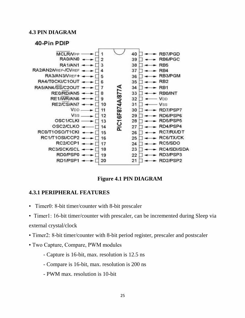
4.3 PIN DIAGRAM
Figure 4.1 PIN DIAGRAM
4.3.1 PERIPHERAL FEATURES
• Timer0: 8-bit timer/counter with 8-bit prescaler
• Timer1: 16-bit timer/counter with prescaler, can be incremented during Sleep via
external crystal/clock
• Timer2: 8-bit timer/counter with 8-bit period register, prescaler and postscaler
• Two Capture, Compare, PWM modules
- Capture is 16-bit, max. resolution is 12.5 ns
- Compare is 16-bit, max. resolution is 200 ns
- PWM max. resolution is 10-bit
26
• Synchronous Serial Port (SSP) with SPI™ (Master mode) and I2C™
(Master/Slave)
• Universal Synchronous Asynchronous Receiver Transmitter (USART/SCI) with
9-bit address detection
• Parallel Slave Port (PSP) – 8 bits wide with external RD, WR and CS controls
(40/44-pin only)
• Brown-out detection circuitry for Brown-out Reset (BOR)
4.3.2 ANALOG FEATURES
• 10-bit, up to 8-channel Analog-to-Digital Converter (A/D)
• Brown-out Reset (BOR)
• Analog Comparator module with:
- Two analog comparators
- Programmable on-chip voltage reference (VREF) module
- Programmable input multiplexing from device inputs and internal voltage
reference
- Comparator outputs are externally accessible
27
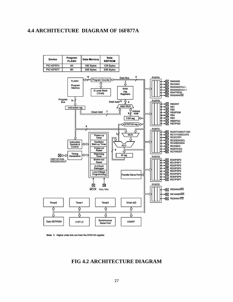
4.4 ARCHITECTURE DIAGRAM OF 16F877A
FIG 4.2 ARCHITECTURE DIAGRAM
28
4.5 MEMORY ORGANIZATION
The memory of a PIC 16F877 chip is divided into 3 sections. They are
Program memory
Data memory and
Data EEPROM
4.5.1. PROGRAM MEMORY
Program memory contains the programs that are written by the user. The
program counter (PC) executes these stored commands one by one. Usually
PIC16F877 devices have a 13 bit wide program counter that is capable of
addressing 8K×14 bit program memory space. This memory is primarily used for
storing the programs that are written (burned) to be used by the PIC. These devices
also have 8K*14 bits of flash memory that can be electrically erasable
/reprogrammed. Each time we write a new program to the controller, we must
delete the old one at that time. The figure below shows the program memory map
and stack.
4.5.2 DATA MEMORY ORGANITATION
The data memory is partitioned into multiple banks which contain the
General Purpose Registers and the Special Function Registers. Bits RP1
(Status<6>) and RP0 (Status<5>) are the bank select bits. Each bank extends up to
7Fh (128 bytes). The lower locations of each bank are reserved for the Special
Function Registers. Above the Special Function Registers are General Purpose
Registers, implemented as static RAM. All implemented banks contain Special
Function Registers. Some frequently used Special Function Registers from one
bank may be mirrored in another bank for code reduction and quicker access.
29
4.6 REGISTERS
The MSSP module has four registers for SPI mode operation. These are:
MSSSP Control Register(SSPCON)
MSSP Status Register(SSPSTAT)
SerialReceive/Transmit Buffer Register(SSPBUF)
Register (SSPSR) – Not directly accessible
SSPCON and SSPSTAT are the control and status registers in SPI mode
operation. The SSPCON register is readable and writable. The lower six bits of the
SSPSTAT are read-only. The upper two bits of the SSPSTAT are read/write.
4.6.1 SPECIAL FUNCTIONS REGISTER
The Special Function Registers are registers used by the CPU and peripheral
modules for controlling the desired operation of the device. The Special Function
Registers can be classified into two sets: core (CPU) and peripheral.
4.6.2 STATUS REGISTER
The Status register contains the arithmetic status of the ALU, the Reset
status and the bank select bits for data memory.
4.6.3 PCON REGISTER
The Power Control (PCON) register contains flag bits to allow
differentiation between a Power-on Reset (POR), a Brown-out Reset (BOR), a
Watchdog Reset (WDT) and an external MCLR Reset.
30
4.6.4 PORTA AND TRISB REGISTER PORTA is a 6-bit wide, bidirectional
port. The corresponding data direction register is TRISA. Setting a TRISA bit (= 1)
will make the corresponding PORTA pin an input (i.e., put the corresponding
output driver in a High-Impedance mode). Clearing a TRISA bit (= 0) will make
the corresponding PORTA pin an output (i.e., put the contents of the output latch
on the selected pin).
4.6.5 PORTB AND TRISB REGISTER
PORTB is an 8-bit wide, bidirectional port. The corresponding data direction
register is TRISB. Setting a TRISB bit (= 1) will make the corresponding PORTB
pin an input (i.e., put the corresponding output driver in a High-Impedance mode).
Clearing a TRISB bit (= 0)
will make the corresponding PORTB pin an output.
4.6.6 PORTC AND TRISC REGISTER
PORTC is an 8-bit wide, bidirectional port. The corresponding data direction
register is TRISC. Setting a TRISC bit (= 1) will make the corresponding PORTC
pin an input (i.e., put the corresponding output driver in a High-Impedance mode).
Clearing a TRISC bit (= 0)
will make the corresponding PORTC pin an output.
4.6.7 PORTD AND TRISD REGISTER
PORTD is an 8-bit port with Schmitt Trigger input buffers. Each pin is
individually configurable as an input or output.

31
PORTD can be configured as an 8-bit wide microprocessor port (Parallel
Slave Port) by setting control bit, PSPMODE (TRISE<4>). In this mode, the input
buffers are TTL.
4.6.8 PORTE AND TRISE REGISTER
PORTE has three pins (RE0/RD/AN5, RE1/WR/AN6 and RE2/CS/AN7)
which are individually configurable as inputs or outputs. These pins have Schmitt
Trigger input buffers.
4.7REAL TIME CLOCK ( DS 1307)
The DS1307 serial real-time clock (RTC) is a low-power, full binary-coded
decimal (BCD) clock/calendar plus 56 bytes of NV SRAM. Address and data are
transferred serially through an I2C, bidirectional bus. The clock operates in either
the 24-hour or 12- hour format with AM/PM indicator.
FIG 4.3 DS130 OPERATING CIRCUIT
32
4.8 ANALOG TO DIGITAL CONVERTER MODULE
The Analog-to-Digital (A/D) Converter module has five inputs for the 28-
pin devices and eight for the 40/44-pin devices.
The conversion of an analog input signal results in a corresponding 10-bit
digital number. The A/D module has high and low-voltage reference input that is
software selectable to some combination of VDD, VSS, RA2 or RA3.
The A/D converter has a unique feature of being able to operate while the
device is in Sleep mode. To operate in Sleep, the A/D clock must be derived from
the A/D‟s internal RC oscillator.
The A/D module has four registers. These registers are:
• A/D Result High Register (ADRESH)
• A/D Result Low Register (ADRESL)
• A/D Control Register 0 (ADCON0)
• A/D Control Register 1 (ADCON1)
The ADCON0 register, shown in Register 11-1, controls the operation of the A/D
module.
The port pins can be configured as analog inputs (RA3 can also be the voltage
reference) or as digital I/O.
4.9 SPECIAL FEATURES OF CPU
All PIC16F87XA devices have a host of features intended to maximize
system reliability, minimize cost through elimination of external components,
provide power saving operating modes and offer code protection. These are:
• Oscillator Selection
• Reset
- Power-on Reset (POR)
- Power-up Timer (PWRT)
33
- Oscillator Start-up Timer (OST)
- Brown-out Reset (BOR)
• Interrupts
• Watchdog Timer (WDT)
• Sleep
• Code Protection
• ID Locations
• In-Circuit Serial Programming
• Low-Voltage In-Circuit Serial Programming
4.10 INSTRUCTION SET
The PIC16 instruction set is highly orthogonal and is comprised of three
basic categories:
•Byte-oriented operations
•Bit-oriented operations
•Literal and control operations
Each PIC16 instruction is a 14-bit word divided into an opcodewhich
specifies the instruction type and one or more operands which further specify the
operation of the instruction.
For byte-oriented instructions, „f‟ represents a file register designator and „d‟
represents a destination designator. The file register designator specifies which file
register is to be used by the instruction.
The destination designator specifies where the result of the operation is to be
placed. If „d‟ is zero, the result is placed in the W register. If „d‟ is one, the result is
placed in the file register specified in the instruction.
34
For bit-oriented instructions, „b‟ represents a bit field designator which
selects the bit affected by the operation, while „f‟ represents the address of the file
in which the bit is located.
For literal and control operations, „k‟ represents an eight or eleven-bit
constant or literal value.
One instruction cycle consists of four oscillator periods; for an oscillator
frequency of 4 MHz, this gives a normal instruction execution time of 1s.
All instructions are executed within a single instruction cycle, unless a
conditional test is true, or the program counter is changed as a result of an
instruction. When this occurs, the execution takes two instruction cycles with the
second cycle executed as a NOP.
35
CHAPTER 5
MECHANICAL SYSTEM
5.1 DC MOTOR
5.1.1 D.C. MOTOR PRINCIPLE
A machine that converts d.c. power into mechanical power is known as a
d.c. motor. Its operation is based on the principle that when a current carrying
conductor is placed in a magnetic field, the conductor experiences a mechanical
force.
5.1.2 WORKING OF D.C. MOTOR
When the terminals of the motor are connected to an external source of d.c.
supply:
(i) The field magnets are excited developing alternate N and S poles
(ii) The armature conductors carry currents. All conductors under N-
pole carry currents in one direction while all the conductors under S-
pole carry currents in the opposite direction.
5.1.3 BACK OR COUNTER E.M.F
When the armature of a d.c. motor rotates under the influence of the driving
torque, the armature conductors move through the magnetic field and hence e.m.f.
is induced in them as in a generator The induced e.m.f. acts in opposite direction to
the applied voltage V (Lenz‟s law) and in known as back or counter e.m.f. Eb. The
back e.m.f. Eb(= P f ZN/60 A) is always less than the applied voltage V, although
this difference is small when the motor is running under normal conditions.
36
5.2 TYPES OF D.C. MOTORS
Like generators, there are three types of d.c. motors characterized by the
connections of field winding in relation to the armature viz.:
(i) Shunt-wound motor in which the field winding is connected in parallel
with the armature. The current through the shunt field winding is not the same as
the armature current. Shunt field windings are designed to produce the necessary
m.m.f. by means of a relatively large number of turns of wire having high
resistance. Therefore, shunt field current is relatively small compared with the
armature current.
(ii) Series-wound motor in which the field winding is connected in series
with the armature. Therefore, series field winding carries the armature current.
Since the current passing through a series field winding is the same as the armature
current, series field windings must be designed with much fewer turns than shunt
field windings for the same m.m.f. Therefore, a series field winding has a relatively
small number of turns of thick wire and, therefore, will possess a low resistance.
(iii) Compound-wound motor which has two field windings; one connected
in parallel with the armature and the other in series with it. There are two types of
compound motor connections (like generators). When the shunt field winding is
directly connected across the armature terminals, it is called short-shunt
connection. When the shunt winding is so connected that it shunts the series
combination of armature and series field, it is called long-shunt connection.
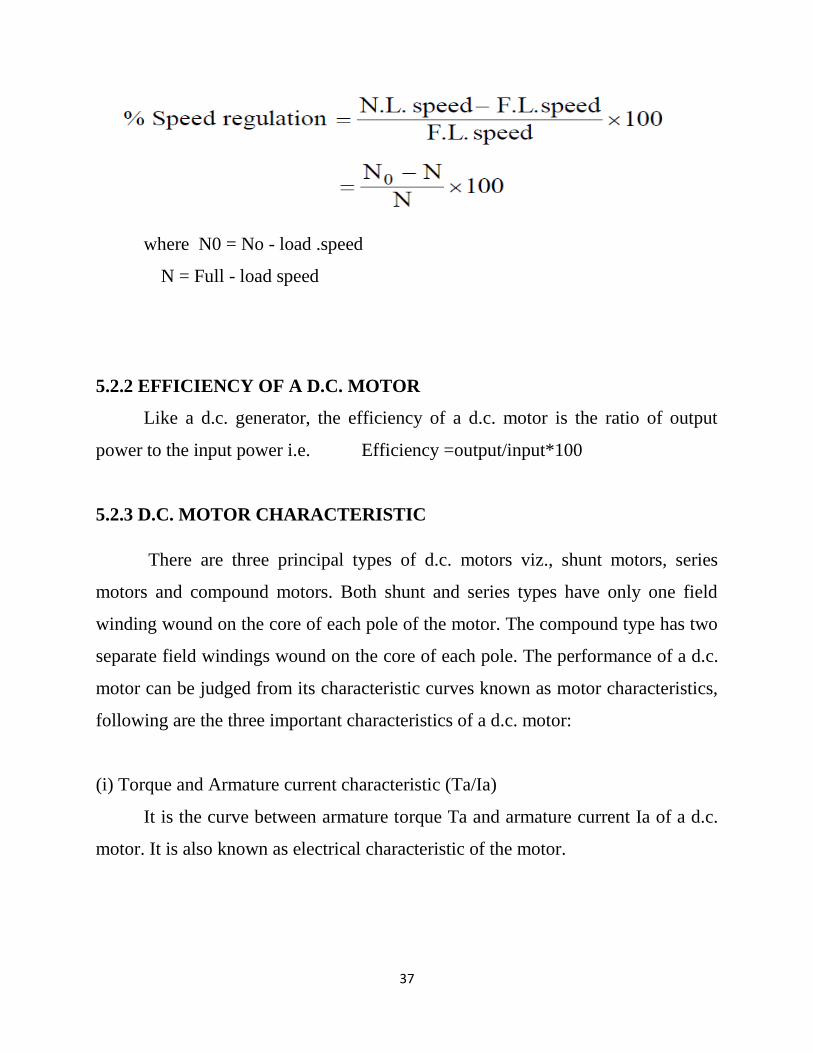
5.2.1 SPEED REGULATION
The speed regulation of a motor is the change in speed from full-load to no-
loud and is expressed as a percentage of the speed at full-load i.e.
37
where N0 = No - load .speed
N = Full - load speed
5.2.2 EFFICIENCY OF A D.C. MOTOR
Like a d.c. generator, the efficiency of a d.c. motor is the ratio of output
power to the input power i.e. Efficiency =output/input*100
5.2.3 D.C. MOTOR CHARACTERISTIC
There are three principal types of d.c. motors viz., shunt motors, series
motors and compound motors. Both shunt and series types have only one field
winding wound on the core of each pole of the motor. The compound type has two
separate field windings wound on the core of each pole. The performance of a d.c.
motor can be judged from its characteristic curves known as motor characteristics,
following are the three important characteristics of a d.c. motor:
(i) Torque and Armature current characteristic (Ta/Ia)
It is the curve between armature torque Ta and armature current Ia of a d.c.
motor. It is also known as electrical characteristic of the motor.
38
(ii) Speed and armature current characteristic (N/Ia)
It is the curve between speed N and armature current Ia of a d.c. motor. It is
very important characteristic as it is often the deciding factor in the selection of the
motor for a particular application.
(iii) Speed and torque characteristic (N/Ta)
It is the curve between speed N and armature torque Ta of a d.c. motor. It is
also known as mechanical characteristic.
39
CHAPTER 6
WIRELESS COMMUNICATION
6.1. HARDWARE MODULE DESCRIPTION
6.2. GENERAL ENCODER AND DECODER OPERATION
The Holtek HT-12E IC encodes 12-bits of information and serially transmits
this data on receipt of a Transmit Enable, or a LOW signal on pin-14 /TE. Pin-17
the D_OUT pin of the HT-12E serially transmits whatever data is available on pins
10,11,12 and 13, or D0,D1,D2 and D3. Data is transmitted at a frequency selected
by the external oscillator resistor. See the encoder/decoder datasheets for details.
Note that if you use anything other than 5V on both encoder/decoder circuits (you
will need to change these oscillator resistor values). Refer to the tables in the
HT12D/HT-12E datasheet.
By using the switches attached to the data pins on the HT-12E, as shown in the
schematic, we can select the information in binary format to send to the receiver.
The receiver section consists of the Ming RE-99 and the HT-12D decoder IC. The
DATA_IN pin-14 of the HT-12D reads the 12-bit binary information sent by the
HT-12E and then places this data on its output pins. Pins 10,11,12 and 13 are the
data out pins of the HT-12D, D0,D1,D2 and D3.
The HT-12D receives the 12-bit word and interprets the first 8-bits as address and
the last 4-bits as data. Pins 1-8 of the HT-12E are the address pins. Using the
address pins of the HT-12E, we can select different addresses for up to 256
receivers. The address is determined by setting pins 1-8 on the HT-12E to ground,
or just leaving them open. The address selected on the HT-12E circuit must match
40
the address selected on the HT-12D circuit (exactly), or the information will be
ignored by the receiving circuit.
When the received addresses from the encoder matches the decoders, the
Valid Transmission pin-17 of the HT-12D will go HIGH to indicate that a valid
transmission has been received and the 4-bits of data are latched to the data output
pins, 10-13. The transistor circuit shown in the schematic will use the VT, or valid
transmission pin to light the LED. When the VT pin goes HIGH it turns on the
2N2222 transistor which in turn delivers power to the LED providing a visual
indication of a valid transmission reception.
6.3. CONTROLING THE PROJECT WITH MICROCONTROLLER
Using these RF transmitter & receiver circuits with a Microcontroller would
be simple. We can simply replace the switches used for selecting data on the HT-
12E with the output pins of the microcontroller. Also we can use another output
pin to select TE, or transmit enable on the HT-12E. By taking pin-14 LOW we
cause the transmitter section to transmit the data on pins 10-13.
To receive information simply hook up the HT-12D output pins to the
microcontroller. The VT, or valid transmission pin of the HT-12D could signal the
microcontroller to grab the 4-bits of data from the data output pins. If you are
using a microcontroller with interrupt capabilities, use the VT pin to cause a jump
to an interrupt vector and process the received data.
The HT-12D data output pins will LATCH and remain in this state until
another valid transmission is received.
41
NOTE: You will notice that in both schematics each of the Holtek chips have
resistors attached to pins 15 and 16. These resistors must be the exact values shown
in the schematic. These resistors set the internal oscillators of the HT-12E/HT-
12D. It is recommended that you choose a 1% resistor for each of these resistors to
ensure the correct circuit oscillation.
6.4. RANGE OF OPERATION
The normal operating range using (only) the LOOP TRACE ANTENNA on
the transmitter board is about 50 feet. By connecting a quarter wave antenna using
9.36 inches of 22 gauge wire to both circuits, you can extend this range to several
hundred feet. Your actual range may vary due to your finished circuit design and
environmental conditions.
The transistors and diodes can be substituted with any common equivalent
type. These will normally depend on the types and capacities of the particular
loads you want to control and should be selected accordingly for your intended
application.
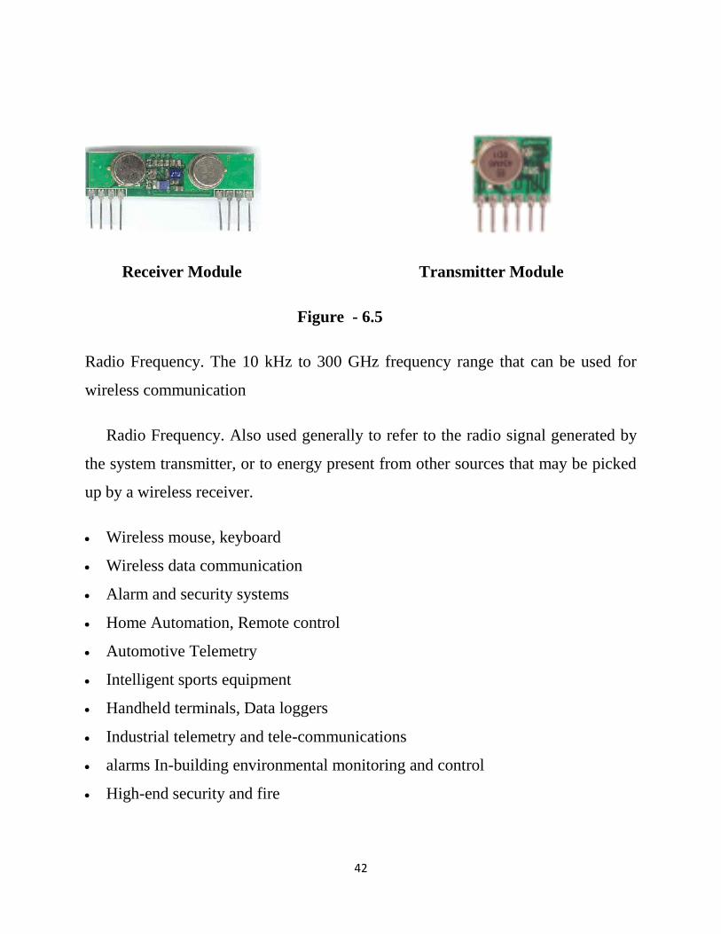
6.5. RF MODULE (RADIO FREQUENCY)
Radio Frequency, any frequency within the electromagnetic spectrum
associated with radio wave propagation. When an RF current is supplied to an
antenna, an electromagnetic field is created that then is able to propagate through
space. Many wireless technologies are based on RF field propagation.
42
Receiver Module Transmitter Module
Figure - 6.5
Radio Frequency. The 10 kHz to 300 GHz frequency range that can be used for
wireless communication
Radio Frequency. Also used generally to refer to the radio signal generated by
the system transmitter, or to energy present from other sources that may be picked
up by a wireless receiver.
Wireless mouse, keyboard
Wireless data communication
Alarm and security systems
Home Automation, Remote control
Automotive Telemetry
Intelligent sports equipment
Handheld terminals, Data loggers
Industrial telemetry and tele-communications
alarms In-building environmental monitoring and control
High-end security and fire
43
6.5.1. TRANSMITTER
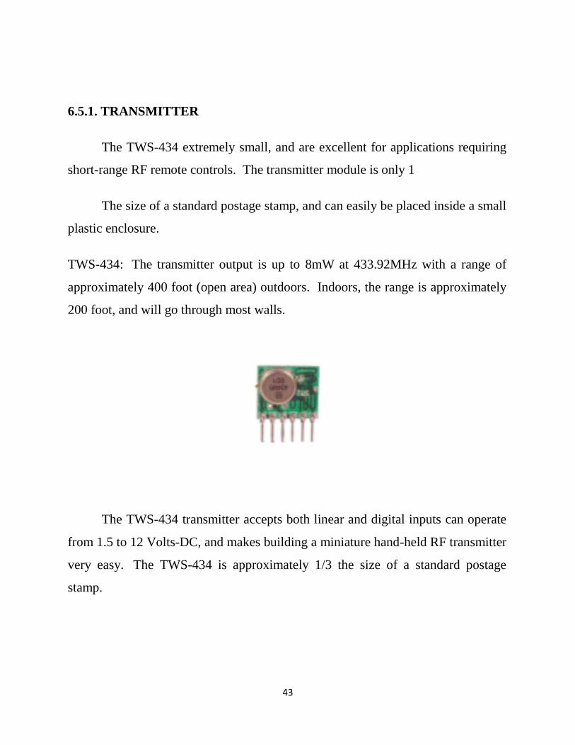
The TWS-434 extremely small, and are excellent for applications requiring
short-range RF remote controls. The transmitter module is only 1
The size of a standard postage stamp, and can easily be placed inside a small
plastic enclosure.
TWS-434: The transmitter output is up to 8mW at 433.92MHz with a range of
approximately 400 foot (open area) outdoors. Indoors, the range is approximately
200 foot, and will go through most walls.
The TWS-434 transmitter accepts both linear and digital inputs can operate
from 1.5 to 12 Volts-DC, and makes building a miniature hand-held RF transmitter
very easy. The TWS-434 is approximately 1/3 the size of a standard postage
stamp.
44
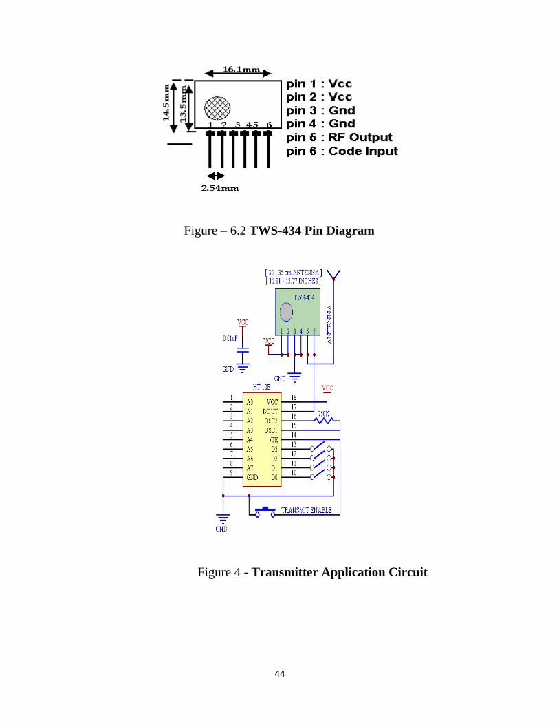
Figure – 6.2 TWS-434 Pin Diagram
Figure 4 - Transmitter Application Circuit
45
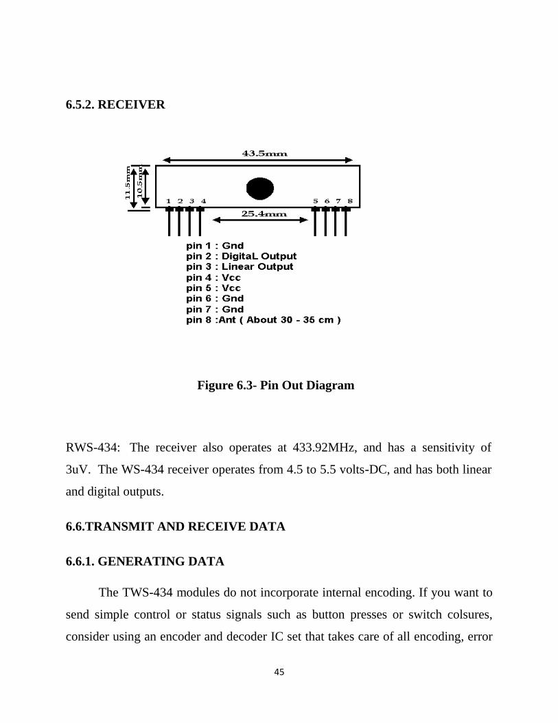
6.5.2. RECEIVER
Figure 6.3- Pin Out Diagram
RWS-434: The receiver also operates at 433.92MHz, and has a sensitivity of
3uV. The WS-434 receiver operates from 4.5 to 5.5 volts-DC, and has both linear
and digital outputs.
6.6.TRANSMIT AND RECEIVE DATA
6.6.1. GENERATING DATA
The TWS-434 modules do not incorporate internal encoding. If you want to
send simple control or status signals such as button presses or switch colsures,
consider using an encoder and decoder IC set that takes care of all encoding, error
46
checking, and decoding functions. These chips are made by Motorola and Holtek.
They are an excellent way to implement basic wireless transmission control.
6.6.2. RECEIVER DATA OUTPUT
A 0 volt to Vcc data output is available on pins. This output is normally used
to drive a digital decoder IC or a microprocessor which is performing the data
decoding. The receiver‟s output will only transition when valid data is present. In
instances when no carrier is present the output will remain low.
6.6.3. DECODINGDATA
The RWS-434 modules do not incorporate internal decoding. If you want to
receive Simple control or status signals such as button presses or switch colsures,
you can use the encoder and decoder IC set described above. Decoders with
momentary and latched outputs are available.
6.6.4. TRANSMITTING AND RECEIVING
Full duplex or simultaneous two-way operation is not possible with these
modules. If a transmit and receive module are in close proximity and data is sent to
a remote receive module while attempting to simultaneously receive data from a
remote transmit module, the receiver will be overloaded by its close proximity
transmitter. This will happen even if encoders and decoders are used with different
address settings for each transmitter and receiver pair. If two way communications
is required, only half duplex operation is allowed.
47
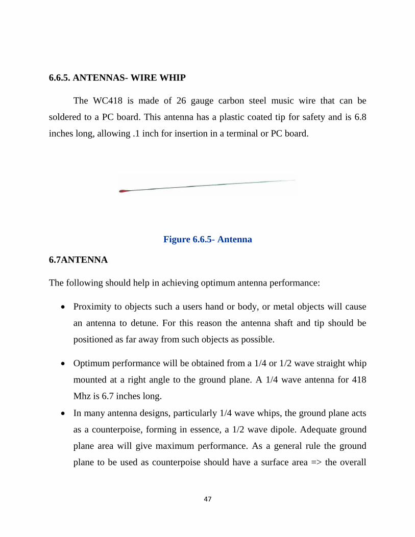
6.6.5. ANTENNAS- WIRE WHIP
The WC418 is made of 26 gauge carbon steel music wire that can be
soldered to a PC board. This antenna has a plastic coated tip for safety and is 6.8
inches long, allowing .1 inch for insertion in a terminal or PC board.
Figure 6.6.5- Antenna
6.7ANTENNA
The following should help in achieving optimum antenna performance:
Proximity to objects such a users hand or body, or metal objects will cause
an antenna to detune. For this reason the antenna shaft and tip should be
positioned as far away from such objects as possible.
Optimum performance will be obtained from a 1/4 or 1/2 wave straight whip
mounted at a right angle to the ground plane. A 1/4 wave antenna for 418
Mhz is 6.7 inches long.
In many antenna designs, particularly 1/4 wave whips, the ground plane acts
as a counterpoise, forming in essence, a 1/2 wave dipole. Adequate ground
plane area will give maximum performance. As a general rule the ground
plane to be used as counterpoise should have a surface area => the overall
48
length of the 1/4 wave radiating element (2.6 X 2.6 inches for a 6.7 inch
long antenna).
Remove the antenna as far as possible from potential interference sources.
Place adequate ground plane under all potential sources of noise.
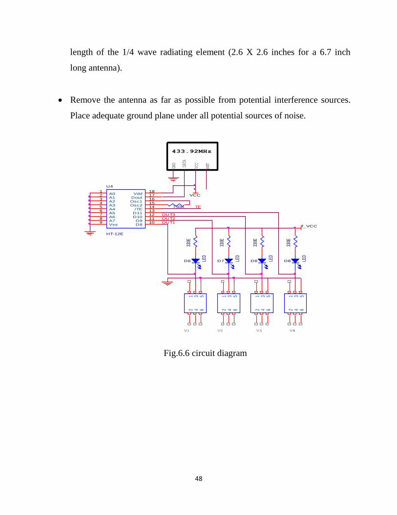
Fig.6.6 circuit diagram
VCC
T_VCC
OUT3
OUT1OUT2
TE
12
34
56
D8 LED
330E
U4
HT-12E
123456789 10
11121314
18171615
A0A1A2A3A4A5A6A7Vss D8
D9D10D11/TE
VddDoutOsc1Osc2 750K
12
34
56
D6 LED
330E
12
34
56
D7 LED
330E
12
34
56
330E
D8 LED
VCC
ANT
V1
DATA
433.92MHz
GND
V2 V3 V4
49
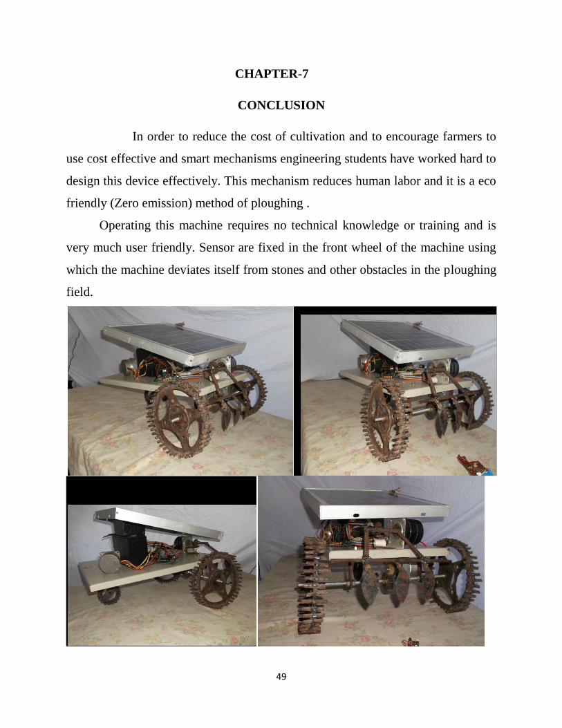
CHAPTER-7
CONCLUSION
In order to reduce the cost of cultivation and to encourage farmers to
use cost effective and smart mechanisms engineering students have worked hard to
design this device effectively. This mechanism reduces human labor and it is a eco
friendly (Zero emission) method of ploughing .
Operating this machine requires no technical knowledge or training and is
very much user friendly. Sensor are fixed in the front wheel of the machine using
which the machine deviates itself from stones and other obstacles in the ploughing
field.
50
REFERENCES
[1] Ford Motor Company, “Let the Sun In: Ford C-MAX Solar Energi Concept
Goes Off the Grid, Gives Glimpse of Clean Vehicle Future | Ford Media Center,”
02-Jan-2014. [Online]. Available:
https://media.ford.com/content/fordmedia/fna/us/en/news/201 4/01/02/let-the-sun-
in--ford-c-max-solar-energi-concept-goesoff- the-gri.html. [Accessed: 14-Jan-
2014].
[2] Webasto, “Webasto: Solar im Fahrzeug,” Solarapplikationen für zukünftige
Fahrzeuge, 2014. [Online]. Available: http://www.webasto-
group.com/de/webastogruppe/ technologien-kompetenzen/solar-im-fahrzeug/.
[Accessed: 20-Jan-2014].
[3] Audi AG, “Solarschiebedach > Audi Deutschland,” Energiemanagement
Solarschiebedach, 2014. [Online]. Available:
http://www.audi.de/de/brand/de/neuwagen/effizienz/effizienzt
echnologien/energiemanagement/solarschiebedach.html. [Accessed: 20-Jan-2014].
[4] Webasto, “Webasto: Solardächer,” Dachsysteme für Hersteller - Solardach,
2014. [Online]. Available: http://www.webasto.com/de/maerkteprodukte/
pkw/dachsysteme-fuer-hersteller/solardaecher/. [Accessed: 20-Jan-2014].
51
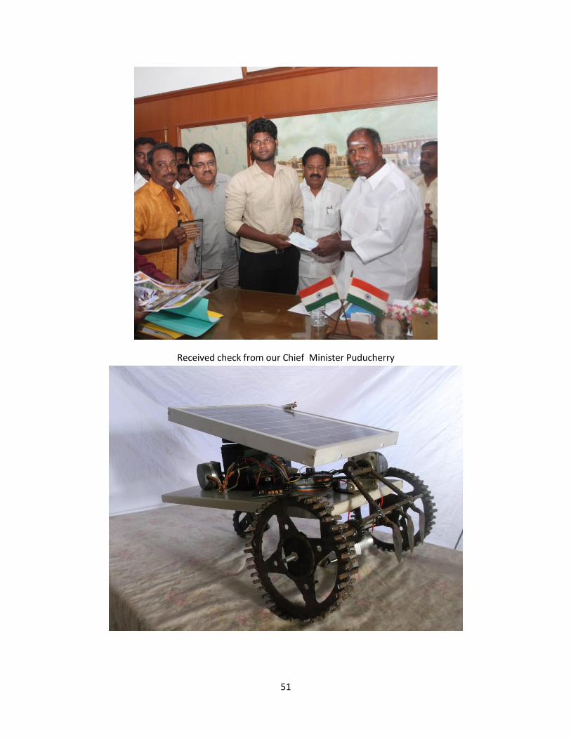
Received check from our Chief Minister Puducherry
52
53