Embed Size (px)
Citation preview
1606383 02 12/2008
1606
383
02
www.schneider-electric.com
Modbus Advantys OTBRemote Inputs/OutputsUser Manual2.0
12/2008

© 2008 Schneider Electric. All rights reserved.
2 1606383 02 12/2008

Table of Contents
Safety Information . . . . . . . . . . . . . . . . . . . . . . . . . . . . . . 7About the Book . . . . . . . . . . . . . . . . . . . . . . . . . . . . . . . . . 9
Chapter 1 Introduction . . . . . . . . . . . . . . . . . . . . . . . . . . . . . . . . . . . 13About Advantys OTB. . . . . . . . . . . . . . . . . . . . . . . . . . . . . . . . . . . . . . . . . 14 Maximum hardware configuration . . . . . . . . . . . . . . . . . . . . . . . . . . . . . . 18Specific Functions of the Network Interface Module . . . . . . . . . . . . . . . . . 21Communication Overview . . . . . . . . . . . . . . . . . . . . . . . . . . . . . . . . . . . . . 22
Chapter 2 Installation. . . . . . . . . . . . . . . . . . . . . . . . . . . . . . . . . . . . . 25Dimensions of the Network Interface Modules . . . . . . . . . . . . . . . . . . . . . 26How to Direct Mount on a Panel . . . . . . . . . . . . . . . . . . . . . . . . . . . . . . . . 27Installation Preparation . . . . . . . . . . . . . . . . . . . . . . . . . . . . . . . . . . . . . . . 28Mounting Positions for the Network Interface Module and the Expansion Modules. . . . . . . . . . . . . . . . . . . . . . . . . . . . . . . . . . . . . . . . . . . . . . . . . . . 29Assembly Precautions for an Island on a Panel or in a Cabinet . . . . . . . . 31Assembly of an Expansion Module to a Network Interface Module . . . . . 32Disassembling an Expansion Module and a Network Interface Module . . 35Removing a Terminal Block . . . . . . . . . . . . . . . . . . . . . . . . . . . . . . . . . . . 36How to Install and Remove a Network Interface Module from a DIN Rail. 38The DIN Rail . . . . . . . . . . . . . . . . . . . . . . . . . . . . . . . . . . . . . . . . . . . . . . . 40
Chapter 3 Description, characteristics, and wiring of the OTB module . . . . . . . . . . . . . . . . . . . . . . . . . . . . . . . . . . . . . . . . 41Wiring Rules and Recommendations . . . . . . . . . . . . . . . . . . . . . . . . . . . . 42Overview of the Network Interface Modules . . . . . . . . . . . . . . . . . . . . . . . 46Physical Description of an Advantys OTB Network Interface Module. . . . 47General Characteristics of the Network Interface Module. . . . . . . . . . . . . 48Network Interface Module I/O Characteristics. . . . . . . . . . . . . . . . . . . . . . 50Wiring diagram for the network interface modules . . . . . . . . . . . . . . . . . . 54How to Connect the Power Supply . . . . . . . . . . . . . . . . . . . . . . . . . . . . . . 55EMC Compatibility. . . . . . . . . . . . . . . . . . . . . . . . . . . . . . . . . . . . . . . . . . . 57Field Bus or Network Connection . . . . . . . . . . . . . . . . . . . . . . . . . . . . . . . 60
1606383 02 12/2008 3

Chapter 4 Description, characteristics, and wiring of the expansion modules . . . . . . . . . . . . . . . . . . . . . . . . . . . . . . 61
4.1 Discrete Expansion Modules . . . . . . . . . . . . . . . . . . . . . . . . . . . . . . . . . . 62Discrete Expansion Modules . . . . . . . . . . . . . . . . . . . . . . . . . . . . . . . . . . 62
4.2 Analog Expansion Modules . . . . . . . . . . . . . . . . . . . . . . . . . . . . . . . . . . . 63Analog Expansion Modules . . . . . . . . . . . . . . . . . . . . . . . . . . . . . . . . . . . 63
4.3 Expansion Module Common Blocks . . . . . . . . . . . . . . . . . . . . . . . . . . . . 64Common Block Expansion Module Wiring Diagrams . . . . . . . . . . . . . . . 64
Chapter 5 Modbus Network Interface of the OTB Module . . . . . . . . 655.1 General Principles . . . . . . . . . . . . . . . . . . . . . . . . . . . . . . . . . . . . . . . . . . 66
Communication on the Modbus Network. . . . . . . . . . . . . . . . . . . . . . . . . 665.2 Cabling on the Modbus Network . . . . . . . . . . . . . . . . . . . . . . . . . . . . . . . 69
Description of the OTB Module Modbus Network Interface. . . . . . . . . . . 70Modbus Field Bus Interface . . . . . . . . . . . . . . . . . . . . . . . . . . . . . . . . . . . 71Network Node Address . . . . . . . . . . . . . . . . . . . . . . . . . . . . . . . . . . . . . . 74Network Speed . . . . . . . . . . . . . . . . . . . . . . . . . . . . . . . . . . . . . . . . . . . . 76Modbus Configuration . . . . . . . . . . . . . . . . . . . . . . . . . . . . . . . . . . . . . . . 78
5.3 Behavior of OTB Modbus Splitter Box . . . . . . . . . . . . . . . . . . . . . . . . . . . 79Managing the Island's Behavior. . . . . . . . . . . . . . . . . . . . . . . . . . . . . . . . 80
Chapter 6 Application-Specific Functions . . . . . . . . . . . . . . . . . . . . 876.1 Island Registers . . . . . . . . . . . . . . . . . . . . . . . . . . . . . . . . . . . . . . . . . . . . 88
Island Registers . . . . . . . . . . . . . . . . . . . . . . . . . . . . . . . . . . . . . . . . . . . . 886.2 Description of the OTB Module I/Os . . . . . . . . . . . . . . . . . . . . . . . . . . . . 92
Description of the OTB Module Discrete I/Os . . . . . . . . . . . . . . . . . . . . . 93Read Input Registers . . . . . . . . . . . . . . . . . . . . . . . . . . . . . . . . . . . . . . . . 94Output Command Registers . . . . . . . . . . . . . . . . . . . . . . . . . . . . . . . . . . 95Advantys OTB Module I/O Parameter Registers . . . . . . . . . . . . . . . . . . . 96
6.3 Specific Functions of the OTB Module. . . . . . . . . . . . . . . . . . . . . . . . . . . 97Specific Functions of the Advantys OTB Modules. . . . . . . . . . . . . . . . . . 98Remote Fast Counter (RFC) Function . . . . . . . . . . . . . . . . . . . . . . . . . . . 99Fast Counter Registers (RFC) . . . . . . . . . . . . . . . . . . . . . . . . . . . . . . . . . 102 Remote Very Fast Counter (RVFC) function . . . . . . . . . . . . . . . . . . . . . 103Remote Very Fast Counter Registers (RVFC). . . . . . . . . . . . . . . . . . . . . 114 Pulse Generator Output Function (RPLS) . . . . . . . . . . . . . . . . . . . . . . . 116Remote Pulse Width Modulator Function (RPWM) . . . . . . . . . . . . . . . . . 120Remote Pulse Generators (RPLS, RPWM) Registers . . . . . . . . . . . . . . . 123
6.4 Discrete I/O of Expansion Modules . . . . . . . . . . . . . . . . . . . . . . . . . . . . . 125Description of the Expansion Module Discrete I/O . . . . . . . . . . . . . . . . . 125
6.5 Analog I/O of Expansion Modules . . . . . . . . . . . . . . . . . . . . . . . . . . . . . . 129Description of the Expansion Module Analog I/O . . . . . . . . . . . . . . . . . . 130TM2 AMI2HT Expansion Module Registers. . . . . . . . . . . . . . . . . . . . . . . 133TM2 AMO1HT Expansion Module Registers . . . . . . . . . . . . . . . . . . . . . . 134TM2 AMM3HT Expansion Module Registers. . . . . . . . . . . . . . . . . . . . . . 135TM2 AMM6HT Expansion Module Registers. . . . . . . . . . . . . . . . . . . . . . 137
4 1606383 02 12/2008
TM2 ALM3LT Expansion Module Registers . . . . . . . . . . . . . . . . . . . . . . . 139TM2 AVO2HT Expansion Module Registers . . . . . . . . . . . . . . . . . . . . . . . 141TM2 AMI2LT Expansion Module Registers. . . . . . . . . . . . . . . . . . . . . . . . 142TM2 AMI4LT Expansion Module Registers. . . . . . . . . . . . . . . . . . . . . . . . 143TM2 AMI8HT Expansion Module Registers . . . . . . . . . . . . . . . . . . . . . . . 144TM2 ARI8HT Expansion Module Registers. . . . . . . . . . . . . . . . . . . . . . . . 146TM2 ARI8LT and TM2 ARI8LRJ Expansion Module Registers. . . . . . . . . 149
Chapter 7 Software Tools . . . . . . . . . . . . . . . . . . . . . . . . . . . . . . . . . 1517.1 Introduction to Software Tools. . . . . . . . . . . . . . . . . . . . . . . . . . . . . . . . . . 152
Introduction . . . . . . . . . . . . . . . . . . . . . . . . . . . . . . . . . . . . . . . . . . . . . . . . 153Software Installation . . . . . . . . . . . . . . . . . . . . . . . . . . . . . . . . . . . . . . . . . 154
7.2 Product Configuration . . . . . . . . . . . . . . . . . . . . . . . . . . . . . . . . . . . . . . . . 155Creating a New Island with the Advantys Configuration Tool . . . . . . . . . . 156Customization of a Memory Area (Registers 1200 to 2199) . . . . . . . . . . . 159Downloading the Modbus Configuration . . . . . . . . . . . . . . . . . . . . . . . . . . 161How to Build Configuration Files? . . . . . . . . . . . . . . . . . . . . . . . . . . . . . . . 163Requests with Twido Soft . . . . . . . . . . . . . . . . . . . . . . . . . . . . . . . . . . . . . 166
Chapter 8 Diagnostics of the Advantys OTB Island . . . . . . . . . . . . 169Indicator Lights (LEDs) . . . . . . . . . . . . . . . . . . . . . . . . . . . . . . . . . . . . . . . 170OTB Island Diagnostic Registers . . . . . . . . . . . . . . . . . . . . . . . . . . . . . . . 172Behavior in the Event of a Fault . . . . . . . . . . . . . . . . . . . . . . . . . . . . . . . . 177
Chapter 9 Island Registers Table . . . . . . . . . . . . . . . . . . . . . . . . . . . 179Registers Table (mapping) for Modbus Advantys OTB Module . . . . . . . . 180I/O Registers . . . . . . . . . . . . . . . . . . . . . . . . . . . . . . . . . . . . . . . . . . . . . . . 182Application-Specific Function Registers . . . . . . . . . . . . . . . . . . . . . . . . . . 184Diagnostic Registers . . . . . . . . . . . . . . . . . . . . . . . . . . . . . . . . . . . . . . . . 188Island Management Registers. . . . . . . . . . . . . . . . . . . . . . . . . . . . . . . . . . 193Customized Zone Registers . . . . . . . . . . . . . . . . . . . . . . . . . . . . . . . . . . . 195Island Module Identification Registers. . . . . . . . . . . . . . . . . . . . . . . . . . . . 196
Appendices . . . . . . . . . . . . . . . . . . . . . . . . . . . . . . . . . . . . . . . . . . . 199Appendix A IEC Symbols . . . . . . . . . . . . . . . . . . . . . . . . . . . . . . . . . . . 201
Glossary of Symbols . . . . . . . . . . . . . . . . . . . . . . . . . . . . . . . . . . . . . . . . . 201
Glossary . . . . . . . . . . . . . . . . . . . . . . . . . . . . . . . . . . . . . . . . . . . 203Index . . . . . . . . . . . . . . . . . . . . . . . . . . . . . . . . . . . . . . . . . . . 207
1606383 02 12/2008 5

6 1606383 02 12/2008

§
Safety InformationImportant Information
NOTICE
Read these instructions carefully, and look at the equipment to become familiar with the device before trying to install, operate, or maintain it. The following special messages may appear throughout this documentation or on the equipment to warn of potential hazards or to call attention to information that clarifies or simplifies a procedure.
1606383 02 12/2008 7

PLEASE NOTE
Electrical equipment should be installed, operated, serviced, and maintained only by qualified personnel. No responsibility is assumed by Schneider Electric for any consequences arising out of the use of this material.
8 1606383 02 12/2008
About the Book
At a Glance
Document Scope
This user manual contains the information for installing an Advantys OTB Modbus network interface module.
It has been designed to facilitate rapid familiarization with the system, while optimizing the system's features for the most advanced technology available.
Anyone installing this equipment must be familiar with the relevant communication protocol, and installation should only be performed by qualified personnel. Special points and warnings regarding safety are highlighted in the different chapters.
The early chapters provide information for designers and installers on installing the mechanical and electrical elements of the system.
The following chapters, from the section on "Modbus network interface", are specific to the communications protocol. They contain information on specific wiring for the network interface and all the necessary information for the software application programmer, and for the end user (diagnostics).
1606383 02 12/2008 9
Record of Revisions:
Validity Note
This user manual applies to V2.0 or later versions of Advantys OTB Modbus modules. For earlier versions, visit http://www.schneider-electric.com.
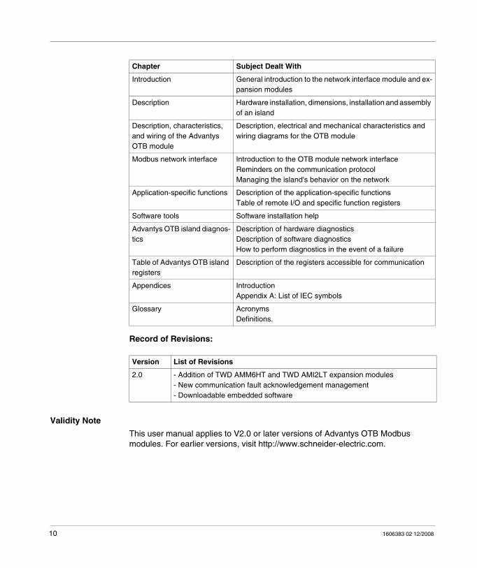
Chapter Subject Dealt With
Introduction General introduction to the network interface module and ex-pansion modules
Description Hardware installation, dimensions, installation and assembly of an island
Description, characteristics, and wiring of the Advantys OTB module
Description, electrical and mechanical characteristics and wiring diagrams for the OTB module
Modbus network interface Introduction to the OTB module network interfaceReminders on the communication protocolManaging the island's behavior on the network
Application-specific functions Description of the application-specific functionsTable of remote I/O and specific function registers
Software tools Software installation help
Advantys OTB island diagnos-tics
Description of hardware diagnosticsDescription of software diagnosticsHow to perform diagnostics in the event of a failure
Table of Advantys OTB island registers
Description of the registers accessible for communication
Appendices IntroductionAppendix A: List of IEC symbols
Glossary AcronymsDefinitions.
Version List of Revisions
2.0 - Addition of TWD AMM6HT and TWD AMI2LT expansion modules- New communication fault acknowledgement management- Downloadable embedded software
10 1606383 02 12/2008

Related Documents
You can download these technical publications and other technical information from our website at www.schneider-electric.com.
User Comments
We welcome your comments about this document. You can reach us by e-mail at [email protected].
Title of Documentation Reference Number
Instruction sheet 1724121
Hardware guide for TM2 discrete I/O expansion modules EIO0000000028
Hardware guide for TM2 analog I/O expansion modules EIO0000000034
Updating embedded OTB software 35015001
FAQ: If you still have questions after reading this guide, visit the FAQ section on http://www.schneider-electric.com.
-
1606383 02 12/2008 11

12 1606383 02 12/2008
1606383 02 12/2008
1
Introduction
1606383 02 12/2008
Introduction
Introduction
This chapter provides an overview of the Advantys OTB network interface modules, the different expansion modules, the maximum configuration and the specific functions of the module, as well as a communication architecture.
What's in this Chapter?
This chapter contains the following topics:
Topic Page
About Advantys OTB 14
Maximum hardware configuration 18
Specific Functions of the Network Interface Module 21
Communication Overview 22
13
Introduction
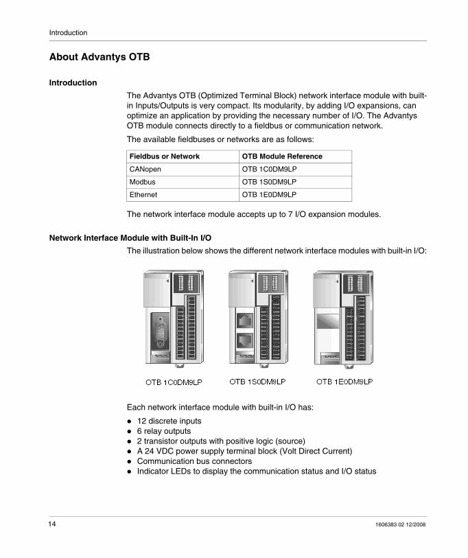
About Advantys OTB
Introduction
The Advantys OTB (Optimized Terminal Block) network interface module with built-in Inputs/Outputs is very compact. Its modularity, by adding I/O expansions, can optimize an application by providing the necessary number of I/O. The Advantys OTB module connects directly to a fieldbus or communication network.
The available fieldbuses or networks are as follows:
The network interface module accepts up to 7 I/O expansion modules.
Network Interface Module with Built-In I/O
The illustration below shows the different network interface modules with built-in I/O:
Each network interface module with built-in I/O has:
12 discrete inputs6 relay outputs2 transistor outputs with positive logic (source)A 24 VDC power supply terminal block (Volt Direct Current)Communication bus connectorsIndicator LEDs to display the communication status and I/O status
Fieldbus or Network OTB Module Reference
CANopen OTB 1C0DM9LP
Modbus OTB 1S0DM9LP
Ethernet OTB 1E0DM9LP
14 1606383 02 12/2008
Introduction
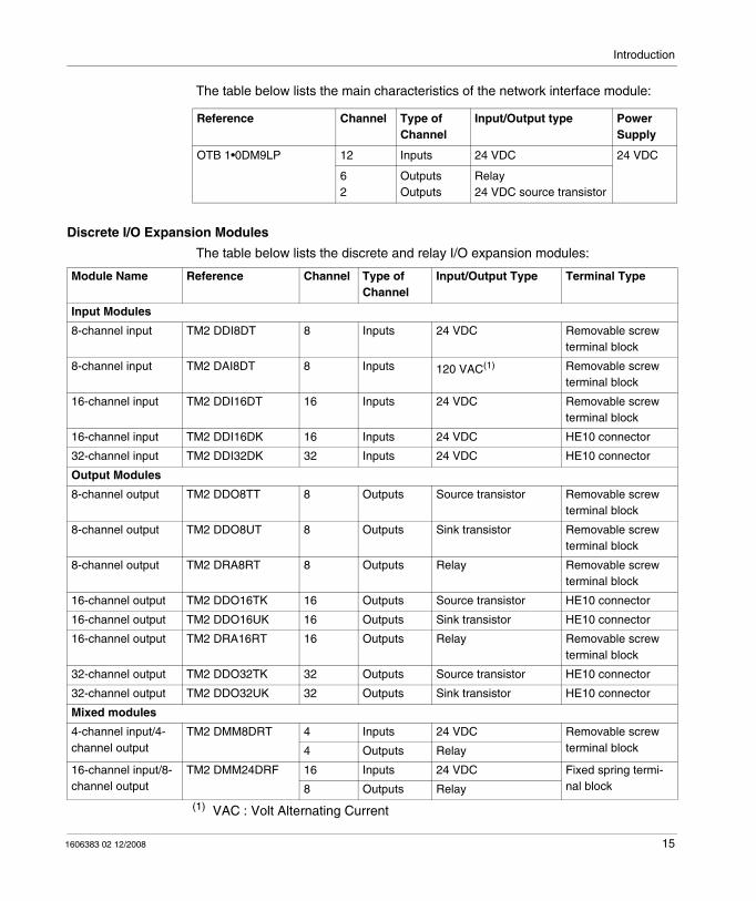
The table below lists the main characteristics of the network interface module:
Discrete I/O Expansion Modules
The table below lists the discrete and relay I/O expansion modules:
(1) VAC : Volt Alternating Current
Reference Channel Type ofChannel
Input/Output type Power Supply
OTB 1•0DM9LP 12 Inputs 24 VDC 24 VDC
62
OutputsOutputs
Relay24 VDC source transistor
Module Name Reference Channel Type ofChannel
Input/Output Type Terminal Type
Input Modules
8-channel input TM2 DDI8DT 8 Inputs 24 VDC Removable screw terminal block
8-channel input TM2 DAI8DT 8 Inputs 120 VAC(1) Removable screw terminal block
16-channel input TM2 DDI16DT 16 Inputs 24 VDC Removable screw terminal block
16-channel input TM2 DDI16DK 16 Inputs 24 VDC HE10 connector
32-channel input TM2 DDI32DK 32 Inputs 24 VDC HE10 connector
Output Modules
8-channel output TM2 DDO8TT 8 Outputs Source transistor Removable screw terminal block
8-channel output TM2 DDO8UT 8 Outputs Sink transistor Removable screw terminal block
8-channel output TM2 DRA8RT 8 Outputs Relay Removable screw terminal block
16-channel output TM2 DDO16TK 16 Outputs Source transistor HE10 connector
16-channel output TM2 DDO16UK 16 Outputs Sink transistor HE10 connector
16-channel output TM2 DRA16RT 16 Outputs Relay Removable screw terminal block
32-channel output TM2 DDO32TK 32 Outputs Source transistor HE10 connector
32-channel output TM2 DDO32UK 32 Outputs Sink transistor HE10 connector
Mixed modules
4-channel input/4-channel output
TM2 DMM8DRT 4 Inputs 24 VDC Removable screw terminal block4 Outputs Relay
16-channel input/8-channel output
TM2 DMM24DRF 16 Inputs 24 VDC Fixed spring termi-nal block8 Outputs Relay
1606383 02 12/2008 15
Introduction
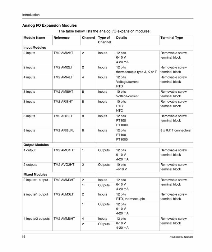
Analog I/O Expansion Modules
The table below lists the analog I/O expansion modules:
Module Name Reference Channel Type of Channel
Details Terminal Type
Input Modules
2 inputs TM2 AMI2HT 2 Inputs 12 bits0-10 V4-20 mA
Removable screw terminal block
2 inputs TM2 AMI2LT 2 Inputs 12 bitsthermocouple type J, K or T
Removable screw terminal block
4 inputs TM2 AMI4LT 4 Inputs 12 bitsVoltage/currentRTD
Removable screw terminal block
8 inputs TM2 AMI8HT 8 Inputs 10 bitsVoltage/current
Removable screw terminal block
8 inputs TM2 ARI8HT 8 Inputs 10 bitsPTCNTC
Removable screw terminal block
8 inputs TM2 ARI8LT 8 Inputs 12 bitsPT100PT1000
Removable screw terminal block
8 inputs TM2 ARI8LRJ 8 Inputs 12 bitsPT100PT1000
8 x RJ11 connectors
Output Modules
1 output TM2 AMO1HT 1 Outputs 12 bits0-10 V4-20 mA
Removable screw terminal block
2 outputs TM2 AVO2HT 2 Outputs 10 bits+/-10 V
Removable screw terminal block
Mixed Modules
2 inputs/1 output TM2 AMM3HT 2 Inputs 12 bits0-10 V4-20 mA
Removable screw terminal block1 Outputs
2 inputs/1 output TM2 ALM3LT 2 Inputs 12 bitsRTD, thermocouple
Removable screw terminal block
1 Outputs 12 bits0-10 V4-20 mA
4 inputs/2 outputs TM2 AMM6HT 4 Inputs 12 bits0-10 V4-20 mA
Removable screw terminal block2 Outputs
16 1606383 02 12/2008
Introduction
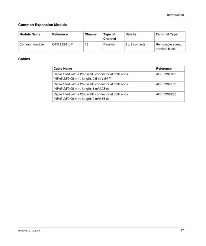
Common Expansion Module
Cables
Module Name Reference Channel Type of Channel
Details Terminal Type
Common module OTB 9ZZ61JP 16 Passive 2 x 8 contacts Removable screw terminal block
Cable Name Reference
Cable fitted with a 20-pin HE connector at both ends.(AWG 28/0.08 mm; length: 0.5 m/1.64 ft)
ABF T20E050
Cable fitted with a 20-pin HE connector at both ends.(AWG 28/0.08 mm; length: 1 m/3.28 ft)
ABF T20E100
Cable fitted with a 20-pin HE connector at both ends.(AWG 28/0.08 mm; length: 2 m/6.56 ft)
ABF T20E200
1606383 02 12/2008 17
Introduction
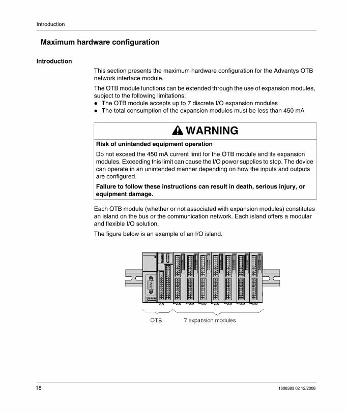
Maximum hardware configuration
Introduction
This section presents the maximum hardware configuration for the Advantys OTB network interface module.
The OTB module functions can be extended through the use of expansion modules, subject to the following limitations:
The OTB module accepts up to 7 discrete I/O expansion modulesThe total consumption of the expansion modules must be less than 450 mA
Each OTB module (whether or not associated with expansion modules) constitutes an island on the bus or the communication network. Each island offers a modular and flexible I/O solution.
The figure below is an example of an I/O island.
WARNINGRisk of unintended equipment operation
Do not exceed the 450 mA current limit for the OTB module and its expansion modules. Exceeding this limit can cause the I/O power supplies to stop. The device can operate in an unintended manner depending on how the inputs and outputs are configured.
Failure to follow these instructions can result in death, serious injury, or equipment damage.
18 1606383 02 12/2008
Introduction
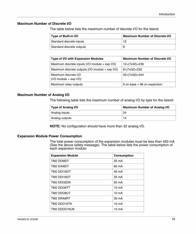
Maximum Number of Discrete I/O
The table below lists the maximum number of discrete I/O for the island:
Maximum Number of Analog I/O
The following table lists the maximum number of analog I/O by type for the island:
NOTE: No configuration should have more than 32 analog I/O.
Expansion Module Power Consumption
The total power consumption of the expansion modules must be less than 450 mA (See the above safety message). The table below lists the power consumption of each expansion module:
Type of Built-in I/O Maximum Number of Discrete I/O
Standard discrete inputs 12
Standard discrete outputs 8
Type of I/O with Expansion Modules Maximum Number of Discrete I/O
Maximum discrete inputs (I/O module + exp I/O) 12+(7x32)=236
Maximum discrete outputs (I/O module + exp I/O) 8+(7x32)=232
Maximum discrete I/O(I/O module + exp I/O)
20+(7x32)=244
Maximum relay outputs 6 on base + 96 on expansion
Type of Analog I/O Maximum Number of Analog I/O
Analog inputs 24
Analog outputs 14
Expansion Module Consumption
TM2 DDI8DT 25 mA
TM2 DAI8DT 60 mA
TM2 DDI16DT 40 mA
TM2 DDI16DT 35 mA
TM2 DDI32DK 65 mA
TM2 DDO8TT 10 mA
TM2 DDO8UT 10 mA
TM2 DRA8RT 30 mA
TM2 DDO16TK 10 mA
TM2 DDDO16UK 10 mA
1606383 02 12/2008 19

Introduction
TM2 DRA16RT 45 mA
TM2 DDO32TK 20 mA
TM2 DDO32UK 20 mA
TM2 DMM8DRT 25 mA
TM2 DMM24DRF 65 mA
TM2 AMI2HT 50 mA
TM2 AMO1HT 50 mA
TM2 AMM3HT 50 mA
TM2 AMM6HT 50 mA
TM2 ALM3LT 50 mA
TM2 AVO2HT 50 mA
TM2 AMI2LT 60 mA
TM2 AMI4LT 50 mA
TM2 AMI8HT 50 mA
TM2 ARI8HT 50 mA
TM2 ARI8LT 90 mA
TM2 ARI8LRJ 90 mA
Expansion Module Consumption
20 1606383 02 12/2008
Introduction
Specific Functions of the Network Interface Module
Introduction
By default, all I/Os of the network interface module are configured as Discrete I/Os. However, certain I/Os can be assigned to remote functions.
Specific Functions
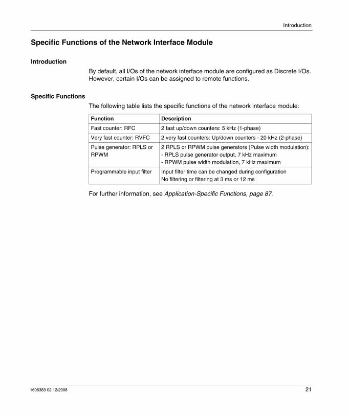
The following table lists the specific functions of the network interface module:
For further information, see Application-Specific Functions, page 87.
Function Description
Fast counter: RFC 2 fast up/down counters: 5 kHz (1-phase)
Very fast counter: RVFC 2 very fast counters: Up/down counters - 20 kHz (2-phase)
Pulse generator: RPLS or RPWM
2 RPLS or RPWM pulse generators (Pulse width modulation):- RPLS pulse generator output, 7 kHz maximum- RPWM pulse width modulation, 7 kHz maximum
Programmable input filter Input filter time can be changed during configurationNo filtering or filtering at 3 ms or 12 ms
1606383 02 12/2008 21
Introduction
Communication Overview
Introduction
The Advantys OTB network interface modules are available for CANopen and Modbus field buses, and for the Ethernet network. They are used to exchange data from the built-in I/Os and expansion module I/Os with the bus master or client.
Field Bus or Network
A module with or without expansion constitutes an I/O island. The network interface module manages data transfers between the island and the master or client, via the field bus or network.
22 1606383 02 12/2008
Introduction
Communication Architecture
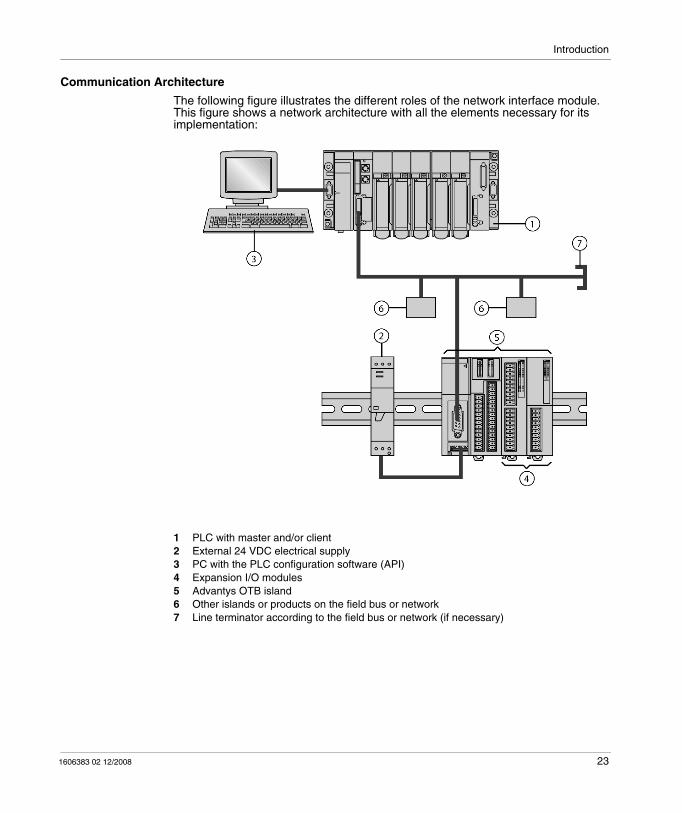
The following figure illustrates the different roles of the network interface module. This figure shows a network architecture with all the elements necessary for its implementation:
1 PLC with master and/or client2 External 24 VDC electrical supply3 PC with the PLC configuration software (API)4 Expansion I/O modules5 Advantys OTB island6 Other islands or products on the field bus or network7 Line terminator according to the field bus or network (if necessary)
1606383 02 12/2008 23

Introduction
24 1606383 02 12/2008
1606383 02 12/2008
2
Installation
1606383 02 12/2008
Installation
Introduction
This chapter provides dimensions, installation, and mounting instructions for Advantys OTB network interface modules, and digital and analog expansion I/O modules.
What's in this Chapter?
This chapter contains the following topics:
Topic Page
Dimensions of the Network Interface Modules 26
How to Direct Mount on a Panel 27
Installation Preparation 28
Mounting Positions for the Network Interface Module and the Expansion Modules
29
Assembly Precautions for an Island on a Panel or in a Cabinet 31
Assembly of an Expansion Module to a Network Interface Module 32
Disassembling an Expansion Module and a Network Interface Module 35
Removing a Terminal Block 36
How to Install and Remove a Network Interface Module from a DIN Rail 38
The DIN Rail 40
25
Installation
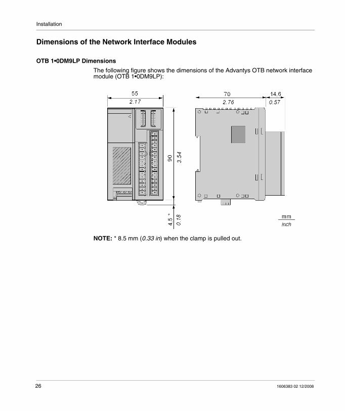
Dimensions of the Network Interface Modules
OTB 1•0DM9LP Dimensions
The following figure shows the dimensions of the Advantys OTB network interface module (OTB 1•0DM9LP):
NOTE: * 8.5 mm (0.33 in) when the clamp is pulled out.
26 1606383 02 12/2008
Installation
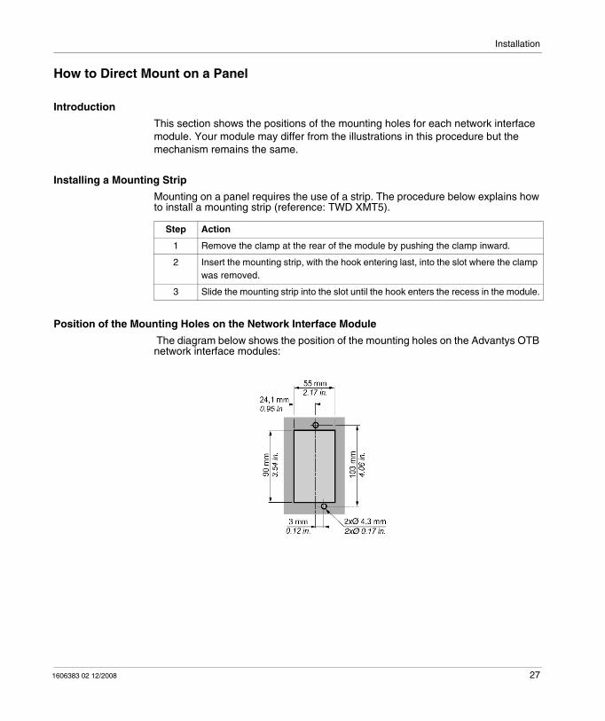
How to Direct Mount on a Panel
Introduction
This section shows the positions of the mounting holes for each network interface module. Your module may differ from the illustrations in this procedure but the mechanism remains the same.
Installing a Mounting Strip
Mounting on a panel requires the use of a strip. The procedure below explains how to install a mounting strip (reference: TWD XMT5).
Position of the Mounting Holes on the Network Interface Module
The diagram below shows the position of the mounting holes on the Advantys OTB network interface modules:
Step Action
1 Remove the clamp at the rear of the module by pushing the clamp inward.
2 Insert the mounting strip, with the hook entering last, into the slot where the clamp was removed.
3 Slide the mounting strip into the slot until the hook enters the recess in the module.
1606383 02 12/2008 27
Installation
Installation Preparation
Introduction
The following section provides information on installing network interface modules and expansion I/O modules.
Before Starting
Before installing network interface modules, read the Safety Information at the beginning of this book.
NOTE: All options and expansion I/O modules should be installed in the network interface module before installing an island on a DIN rail, on a mounting plate, or in a cabinet. The island should be removed from a DIN rail, a mounting plate or a cabinet before disassembling the different modules.
WARNINGRISK OF UNINTENDED EQUIPMENT OPERATION
Do not add or remove an expansion module to or from the system before first removing all power. Adding or removing an expansion module while under power may cause damage to the module and the system, resulting in unexpected operation of inputs and outputs. Depending on I/O configuration, unintended equipment operation may occur.
Failure to follow these instructions can result in death, serious injury, or equipment damage.
28 1606383 02 12/2008
Installation
Mounting Positions for the Network Interface Module and the Expansion Modules
Introduction
This section shows the correct and incorrect mounting positions for all network interface modules and expansion I/O modules.
WARNINGRISK OF UNEXPECTED EQUIPMENT OPERATION
Keep adequate spacing around the island for proper ventilation and to maintain an ambient temperature between 0 °C(32°F) and 55 °C (131°F). Overheating of the OTB module and/or the I/O expansion modules may result in unexpected operation of inputs and outputs.
Depending on the I/O configuration, unintended equipment operation may occur.
Failure to follow these instructions can result in death, serious injury, or equipment damage.
WARNINGRISK OF UNEXPECTED EQUIPMENT OPERATION
Do not place heat generating devices such as transformers and supply blocks under the island. Heat generating devices in the proximity of the OTB module and I/O expansion modules could result in elevated temperatures and overheating, and may result in unexpected operation of the inputs and outputs. Depending on the I/O configuration, unexpected equipment operation may occur.
Failure to follow these instructions can result in death, serious injury, or equipment damage.
1606383 02 12/2008 29
Installation
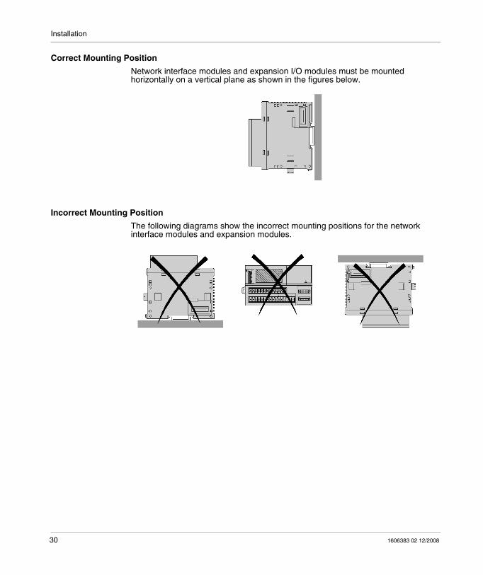
Correct Mounting Position
Network interface modules and expansion I/O modules must be mounted horizontally on a vertical plane as shown in the figures below.
Incorrect Mounting Position
The following diagrams show the incorrect mounting positions for the network interface modules and expansion modules.
30 1606383 02 12/2008
Installation
Assembly Precautions for an Island on a Panel or in a Cabinet
Introduction
This section presents the assembly precautions required for islands on a control panel or in a cabinet.
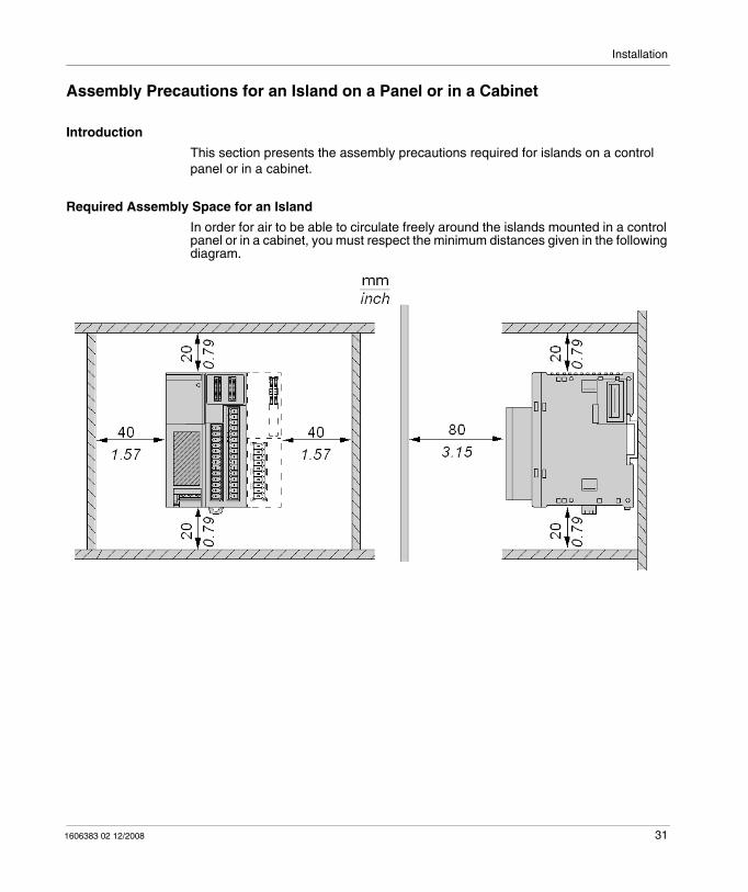
Required Assembly Space for an Island
In order for air to be able to circulate freely around the islands mounted in a control panel or in a cabinet, you must respect the minimum distances given in the following diagram.
1606383 02 12/2008 31
Installation
Assembly of an Expansion Module to a Network Interface Module
Introduction
This section shows how to assemble an expansion module to a network interface module. Your network interface module or expansion module may differ to the ones shown in the illustrations for this procedure, but the mechanism remains the same.
WARNINGRISK OF UNEXPECTED EQUIPMENT OPERATION
Do not change the hardware configuration without updating both the master device and the client application program. Do not reapply power after reconfiguring hardware until all updates to the master device and client application program have been accomplished and confirmed.
Failure to make these required updates may cause unintended operation of the inputs and outputs. Depending on I/O configuration, unintended equipment operation may result.
Failure to follow these instructions can result in death, serious injury, or equipment damage.
32 1606383 02 12/2008
Installation
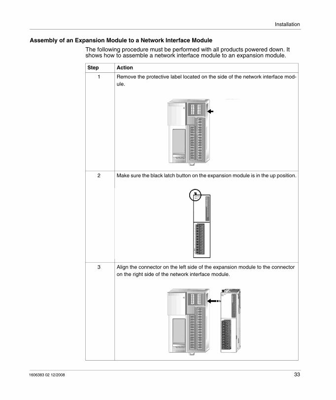
Assembly of an Expansion Module to a Network Interface Module
The following procedure must be performed with all products powered down. It shows how to assemble a network interface module to an expansion module.
Step Action
1 Remove the protective label located on the side of the network interface mod-ule.
2 Make sure the black latch button on the expansion module is in the up position.
3 Align the connector on the left side of the expansion module to the connector on the right side of the network interface module.
1606383 02 12/2008 33
Installation
4 Press the expansion module to the network interface module until it "clicks" into place.
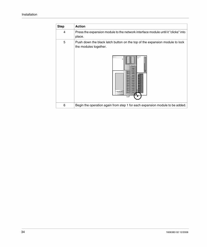
5 Push down the black latch button on the top of the expansion module to lock the modules together.
6 Begin the operation again from step 1 for each expansion module to be added.
Step Action
34 1606383 02 12/2008
Installation
Disassembling an Expansion Module and a Network Interface Module
Introduction
This section shows how to disassemble an expansion interface from a network interface module. Your network interface module or expansion module may differ to the ones shown in the illustrations for this procedure, but the mechanism remains the same.
Disassembly of an Expansion Module from a Network Interface Module
The following procedure must be performed with all products powered down. It shows how to disassemble an expansion module from a network interface module.
Step Action
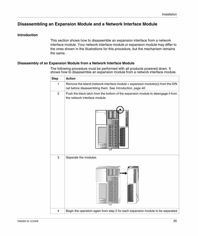
1 Remove the island (network interface module + expansion module(s)) from the DIN rail before disassembling them. See Introduction, page 40.
2 Push the black latch from the bottom of the expansion module to disengage it from the network interface module.
3 Separate the modules.
4 Begin the operation again from step 2 for each expansion module to be separated.
1606383 02 12/2008 35
Installation
Removing a Terminal Block
Introduction
This section describes the removal of terminal blocks from Advantys OTB network interface modules.
Removing a Terminal Block
The following procedure describes how to remove terminal blocks from the network interface module.
Step Action
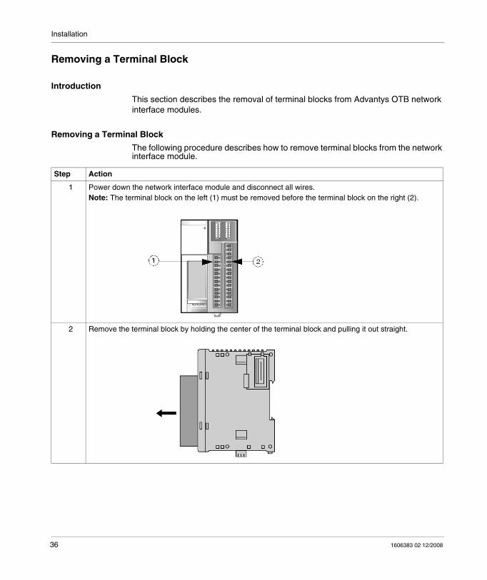
1 Power down the network interface module and disconnect all wires.Note: The terminal block on the left (1) must be removed before the terminal block on the right (2).
2 Remove the terminal block by holding the center of the terminal block and pulling it out straight.
36 1606383 02 12/2008

Installation
CAUTIONRISK OF EQUIPMENT DAMAGE
Do not attempt to remove the terminal by pulling on its top or bottom surfaces. Only pull on the terminal from the sides. Pulling from the top or bottom may cause the terminal to exit at an angle and damage the connector pins.
Failure to follow these instructions can result in injury or equipment damage.
1606383 02 12/2008 37
Installation
How to Install and Remove a Network Interface Module from a DIN Rail
Introduction
This section shows how to install and remove an island from a DIN rail. Your island may differ from the illustrations in this procedure but the mechanism is the same.
NOTE: When mounting modules on a DIN rail, use two end stops, type AB1AB8P35 or equivalent.
Installing an Island on a DIN Rail
The following procedure must be performed with all products powered down. It describes how to install an island on a DIN rail.
Step Action
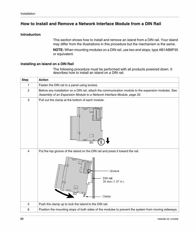
1 Fasten the DIN rail to a panel using screws.
2 Before any installation on a DIN rail, attach the communication module to the expansion modules. See Assembly of an Expansion Module to a Network Interface Module, page 33.
3 Pull out the clamp at the bottom of each module.
4 Put the top groove of the island on the DIN rail and press it toward the rail.
5 Push the clamp up to lock the island to the DIN rail.
6 Position the mounting stops of both sides of the modules to prevent the system from moving sideways.
38 1606383 02 12/2008
Installation
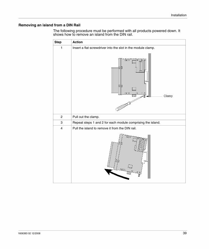
Removing an island from a DIN Rail
The following procedure must be performed with all products powered down. It shows how to remove an island from the DIN rail.
Step Action
1 Insert a flat screwdriver into the slot in the module clamp.
2 Pull out the clamp.
3 Repeat steps 1 and 2 for each module comprising the island.
4 Pull the island to remove it from the DIN rail.
1606383 02 12/2008 39
Installation
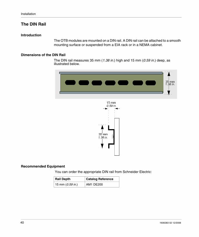
The DIN Rail
Introduction
The OTB modules are mounted on a DIN rail. A DIN rail can be attached to a smooth mounting surface or suspended from a EIA rack or in a NEMA cabinet.
Dimensions of the DIN Rail
The DIN rail measures 35 mm (1.38 in.) high and 15 mm (0.59 in.) deep, as illustrated below.
Recommended Equipment
You can order the appropriate DIN rail from Schneider Electric:
Rail Depth Catalog Reference
15 mm (0.59 in.) AM1 DE200
40 1606383 02 12/2008
1606383 02 12/2008
3
Description, characteristics, and wiring of the OTB module
1606383 02 12/2008
Description, characteristics, and wiring of the OTB module
Introduction
This chapter describes the wiring rules and recommendations, overviews, part references, characteristics and wiring diagrams for the Advantys OTB network interface module.
What's in this Chapter?
This chapter contains the following topics:
Topic Page
Wiring Rules and Recommendations 42
Overview of the Network Interface Modules 46
Physical Description of an Advantys OTB Network Interface Module 47
General Characteristics of the Network Interface Module 48
Network Interface Module I/O Characteristics 50
Wiring diagram for the network interface modules 54
How to Connect the Power Supply 55
EMC Compatibility 57
Field Bus or Network Connection 60
41
Description, characteristics, and wiring of the OTB module
Wiring Rules and Recommendations
Introduction
There are several rules that must be followed when wiring a module or network interface. Recommendations, when needed, are provided on how to comply with the rules.
Rules
Each connector terminal accepts up to two wires fitted with cable ends or tags,
with sections between 0.14 mm2 and 1.5 mm2, (AWG26 and AWG16).Output module fusing is the responsibility of the user. It is not within the OTB network interface module itself. Select a fuse appropriate for the load with respect to the electrical codes.Depending on the load, a protection circuit may be needed for relay outputs on modules.
The power supply wire should be between 0.14 mm2 and 1.5 mm2(AWG26 and AWG16). Use the shortest wire length possible.
The grounding wire should be 1.50 mm2 (AWG16).Be sure to connect the grounding wire to a proper ground.Power supply wires routed inside the panel must be kept separate from I/O and communication wiring. Route wiring in separate cable ducting.
DANGERELECTRIC SHOCK
Be sure to remove ALL power from ALL devices before connecting or disconnecting inputs or outputs to any terminal or installing or removing any hardware.Make sure you have COMPLETELY powered down ALL devices before connecting or disconnecting the bus or network.
Failure to follow these instructions will result in death or serious injury.
WARNINGRISK OF UNINTENDED EQUIPMENT OPERATION
If outputs should fail, outputs may remain on or off. Where personnel and or equipment hazards exist, use an appropriate hard-wired safety system.
Failure to follow these instructions can result in death, serious injury, or equipment damage.
42 1606383 02 12/2008
Description, characteristics, and wiring of the OTB module
Take care when wiring output modules that are designed to work as either source or sink. Incorrect wiring can cause equipment damage.Make sure that the operating conditions and environments are within the specification values.Use proper wire size to meet voltage and current requirements.Fit cable ends to the cables.
Contact Protection Circuit for Relay and Transistor Outputs
Depending on the load, a protection circuit may be needed for relay outputs. Choose a protection circuit, from the following diagrams, according to the power supply. Connect the protection circuit to the outside of the module for the relay outputs.
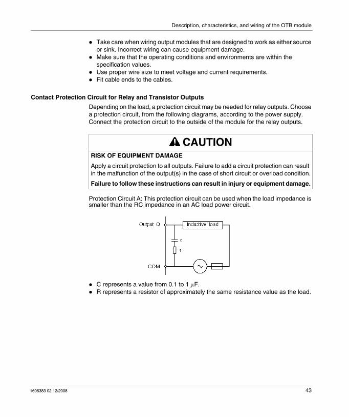
Protection Circuit A: This protection circuit can be used when the load impedance is smaller than the RC impedance in an AC load power circuit.
C represents a value from 0.1 to 1 μF.R represents a resistor of approximately the same resistance value as the load.
CAUTIONRISK OF EQUIPMENT DAMAGE
Apply a circuit protection to all outputs. Failure to add a circuit protection can result in the malfunction of the output(s) in the case of short circuit or overload condition.
Failure to follow these instructions can result in injury or equipment damage.
1606383 02 12/2008 43
Description, characteristics, and wiring of the OTB module
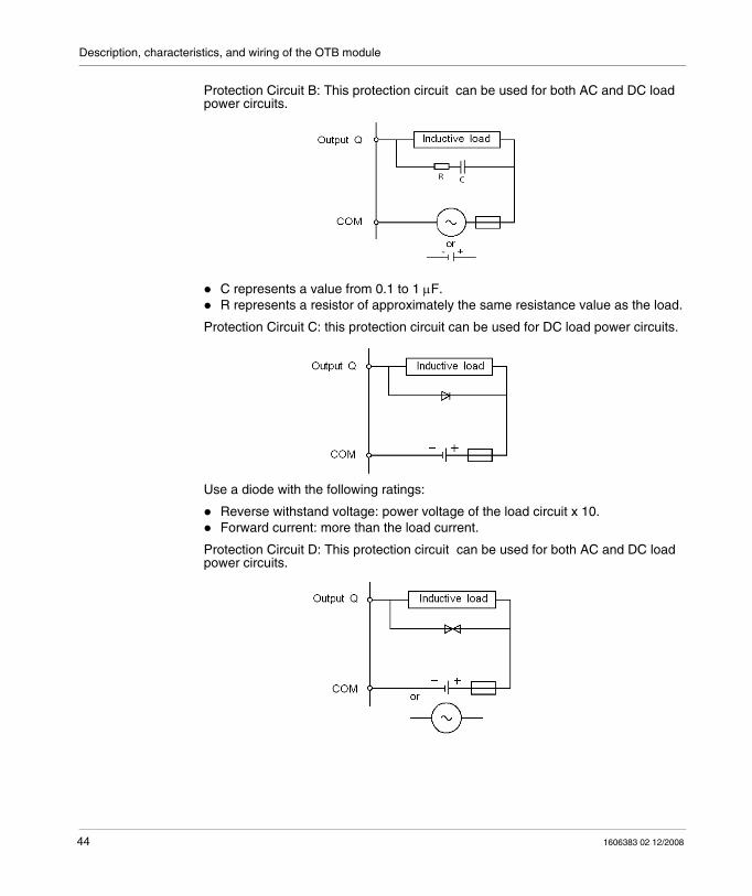
Protection Circuit B: This protection circuit can be used for both AC and DC load power circuits.
C represents a value from 0.1 to 1 μF.R represents a resistor of approximately the same resistance value as the load.
Protection Circuit C: this protection circuit can be used for DC load power circuits.
Use a diode with the following ratings:
Reverse withstand voltage: power voltage of the load circuit x 10.Forward current: more than the load current.
Protection Circuit D: This protection circuit can be used for both AC and DC load power circuits.
44 1606383 02 12/2008
Description, characteristics, and wiring of the OTB module
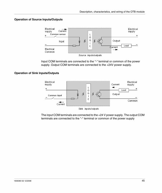
Operation of Source Inputs/Outputs
Input COM terminals are connected to the "-" terminal or common of the power supply. Output COM terminals are connected to the +24V power supply.
Operation of Sink Inputs/Outputs
The input COM terminals are connected to the +24 V power supply. The output COM terminals are connected to the "-" terminal or common of the power supply
1606383 02 12/2008 45
Description, characteristics, and wiring of the OTB module
Overview of the Network Interface Modules
Introduction
This section describes the entire range of Advantys OTB network interface modules.
Illustrations
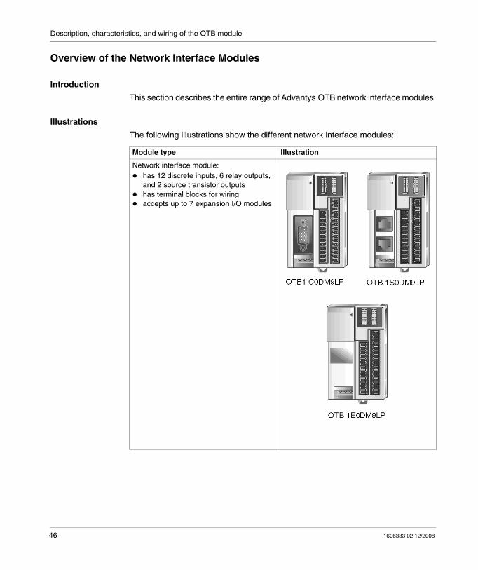
The following illustrations show the different network interface modules:
Module type Illustration
Network interface module:has 12 discrete inputs, 6 relay outputs, and 2 source transistor outputshas terminal blocks for wiringaccepts up to 7 expansion I/O modules
46 1606383 02 12/2008
Description, characteristics, and wiring of the OTB module
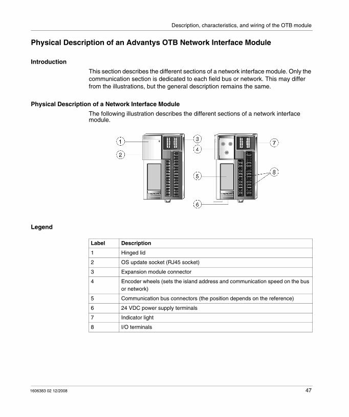
Physical Description of an Advantys OTB Network Interface Module
Introduction
This section describes the different sections of a network interface module. Only the communication section is dedicated to each field bus or network. This may differ from the illustrations, but the general description remains the same.
Physical Description of a Network Interface Module
The following illustration describes the different sections of a network interface module.
Legend
Label Description
1 Hinged lid
2 OS update socket (RJ45 socket)
3 Expansion module connector
4 Encoder wheels (sets the island address and communication speed on the bus or network)
5 Communication bus connectors (the position depends on the reference)
6 24 VDC power supply terminals
7 Indicator light
8 I/O terminals
1606383 02 12/2008 47
Description, characteristics, and wiring of the OTB module
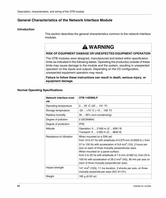
General Characteristics of the Network Interface Module
Introduction
This section describes the general characteristics common to the network interface modules.
Normal Operating Specifications
WARNINGRISK OF EQUIPMENT DAMAGE OR UNEXPECTED EQUIPMENT OPERATION
The OTB modules were designed, manufactured and tested within specification limits as indicated in the following tables. Operating the product(s) outside of these limits may cause damage to the module and the system, resulting in unexpected operation on the inputs and outputs. Depending on the I/O configuration, unexpected equipment operation may result.
Failure to follow these instructions can result in death, serious injury, or equipment damage.
Network interface mod-ule
OTB 1•0DM9LP
Operating temperature 0 ... 55 °C (32 ... 131 °F)
Storage temperature -25 ... +70 °C (-13 ... 158 °F)
Relative humidity 30 ... 95% (non-condensing)
Degree of pollution 2 (IEC60664)
Degree of protection IP20
Altitude Operation: 0 ... 2 000 m (0 ... 6561 ft)Transport: 0 ... 3 000 m (0 ... 9842 ft)
Resistance to Vibration When mounted on a DIN rail:from 10 to 57 Hz with amplitude of 0.075 mm (0.0029 in.), from
57 to 150 Hz with acceleration of 9.8 m/s2 (1G), 2 hours per axis on each of three mutually perpendicular axes.When mounted on a panel surface:from 2 to 25 Hz with amplitude of 1.6 mm (0.062 in), from 25 to
100 Hz with acceleration of 39.2 m/s2 (4G), 90 min per axis on each of three mutually perpendicular axes.
Impact strength 147 m/s2 (15G), 11 ms duration, 3 shocks per axis, on three mutually perpendicular axes (IEC 61131).
Weight 185 g (6.52 oz)
48 1606383 02 12/2008
Description, characteristics, and wiring of the OTB module
Electrical Characteristics
Network interface module
OTB 1•0DM9LP
Rated power voltage 24 VDC
Allowable voltage range 20,4 ... 26.4 VDC (including ripple)
Consumed power Communication module with 7 expansion modules
19 W (26.4 VDC)
Allowable momentary pow-er interruption
10 ms (24 VDC)
Dielectric strength Between power and ground terminals: 500 VAC, 1 minBetween I/O and ground terminals: 500 VAC, 1 min
Insulation resistance Between power and ground terminals: 10 MΩ minimum (500 VDC)Between I/O and ground terminals:10 MΩ minimum (500 VDC)
Noise resistanceIEC 1131-2
DC power terminals: 1 kV, 50 ns to 1 μsI/O terminals (coupling clamp): 1,5 kV, 50 ns to 1 μs
Inrush current 50 A maximum (24 VDC)
Ground wiring 1 mm2 (AWG 18), 1.5 mm2 (AWG 16)
Power supply wiring 0.14 mm2 (AWG 26), 1.5 mm2 (AWG 16)
Tightening torque of the 24 VDC supply terminals
0.8 Nm (7.08 lb-in)
Tightening torque of the I/O terminals
0.6 Nm (5.31 lb-in)
1606383 02 12/2008 49
Description, characteristics, and wiring of the OTB module
Network Interface Module I/O Characteristics
Introduction
This section describes the characteristics of the Advantys OTB network interface module I/O.
Input Characteristics
Network Interface Module OTB 1•0DM9LP
Number of inputs 12 inputs with common
Nominal input voltage 24 VDC source/sink input signal
Input voltage range 20.4 ... 26.4 VDC
Nominal input current I0, I1, I6, I7: 5 mA/input (24 VDC)I2 to I5, I8 to I11: 7 mA/input (24 VDC)
Input impedance I0, I1, I6, I7: 5 kΩI2 to I5, I8 to I11: 3.4 kΩ
Switching time at high state(ON Time)
I0 to I7: 35 μs + filter valueI8 to I11: 40 μs + filter value
Switching time at low state(OFF Time)
I0, I1, I6, I7: 45 μs + filter valueI2 to I5, I8 to I11: 150 μs + filter value
Isolation Between input terminals: not isolatedInternal circuit: Optocoupler isolated (up to 500 VAC rms)
Filtering: 3 possibilitiesNone3 ms12 ms
I0 to I11
Input type Type 1 (IEC 61131)
External load for I/O interconnection Not needed
Signal determination method Static
Effect of incorrect input connection The input signals can be both sink and source. But if any input ex-ceeding the nominal value is applied, permanent damage may be caused. In all cases, the user is responsible for the wiring.
Input cable length 30 m (98.4 ft) for compliance with electromagnetic immunity
Average number of connector insertions/removals 100 times minimum
50 1606383 02 12/2008
Description, characteristics, and wiring of the OTB module
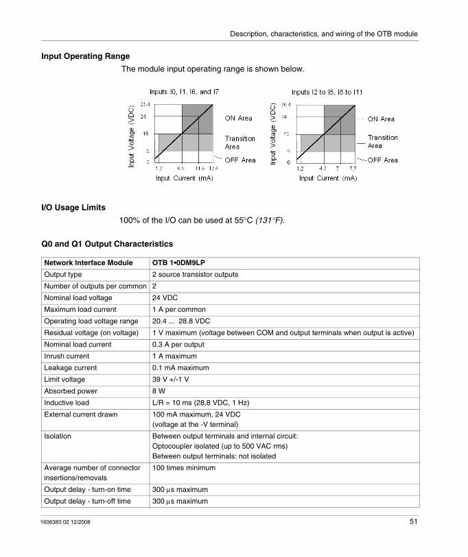
Input Operating Range
The module input operating range is shown below.
I/O Usage Limits
100% of the I/O can be used at 55°C (131°F).
Q0 and Q1 Output Characteristics
Network Interface Module OTB 1•0DM9LP
Output type 2 source transistor outputs
Number of outputs per common 2
Nominal load voltage 24 VDC
Maximum load current 1 A per common
Operating load voltage range 20.4 ... 28.8 VDC
Residual voltage (on voltage) 1 V maximum (voltage between COM and output terminals when output is active)
Nominal load current 0.3 A per output
Inrush current 1 A maximum
Leakage current 0.1 mA maximum
Limit voltage 39 V +/-1 V
Absorbed power 8 W
Inductive load L/R = 10 ms (28.8 VDC, 1 Hz)
External current drawn 100 mA maximum, 24 VDC(voltage at the -V terminal)
Isolation Between output terminals and internal circuit: Optocoupler isolated (up to 500 VAC rms)Between output terminals: not isolated
Average number of connector insertions/removals
100 times minimum
Output delay - turn-on time 300 μs maximum
Output delay - turn-off time 300 μs maximum
1606383 02 12/2008 51
Description, characteristics, and wiring of the OTB module
Q2 to Q7 Output Characteristics
(*) for AC1 & DC1 the powers indicated here take account of the maximum per point on OTB (2A).
Network Interface Module OTB 1•0DM9LP
Output type 6 relay outputs
Number of outputs per common - COM0 2 outputs
Number of outputs per common - COM1 3 NO contacts
Number of outputs per common - COM2 2 NO contacts
Number of outputs per common - COM3 1 NO contact
Maximum load current 2 A per output8 A per common
Minimum switching load 0.1 mA/0.1 VDC (reference value)
Initial contact resistance 30 mΩ maximum
Mechanical life 20,000,000 operations minimum (estimated load 18,000 opera-tions/hr)
Dielectric strength 1500 VACrms between the output and internal circuit, 1 min750 VACrms between the output and COM terminal, 1 min
Average number of connector insertions/removals 100 times minimum
Closing delay 5 ms typ, 10 ms max
Opening delay 2 ms typ, 5 ms max
Closing bounce time 1 ms maximum
Operating Category Nominal Load Electrical Life (Number of Operations)
AC1Resistive load control
500 VA(*) 105
AC14Weak electromagnet load
250 VA 105
AC15Electromagnet
200 VA 105
DC1Resistive load control
60 W(*) 105
DC13Electromagnet L/R=150 ms
30 W 105
52 1606383 02 12/2008
Description, characteristics, and wiring of the OTB module
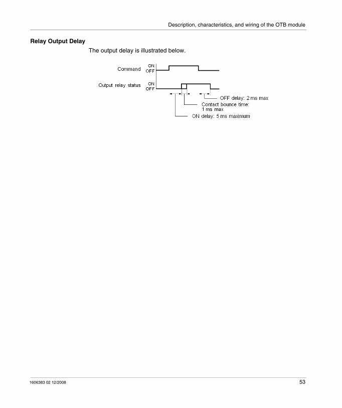
Relay Output Delay
The output delay is illustrated below.
1606383 02 12/2008 53
Description, characteristics, and wiring of the OTB module
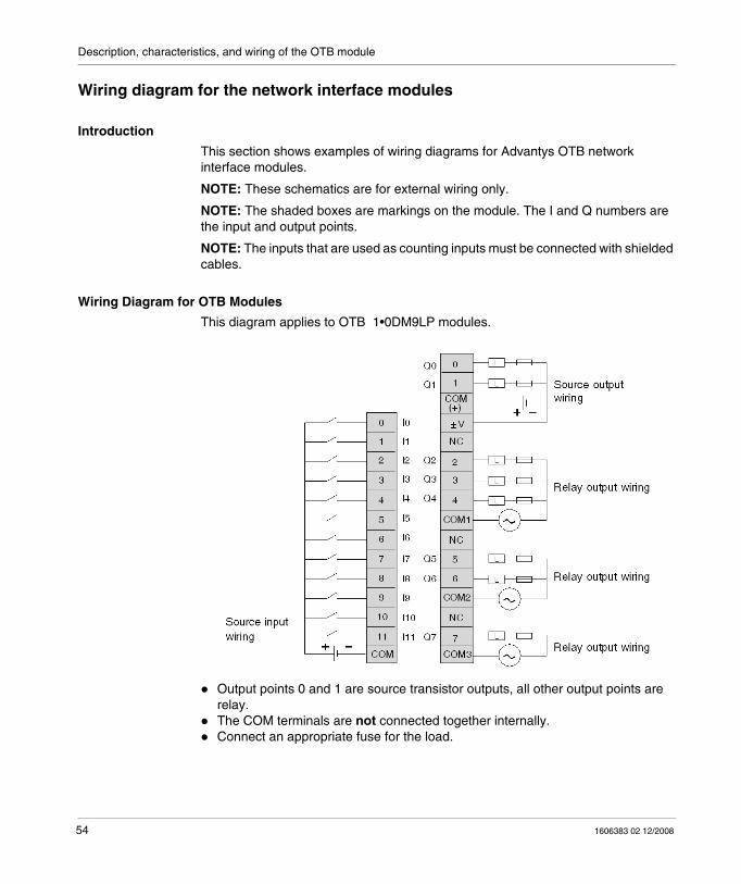
Wiring diagram for the network interface modules
Introduction
This section shows examples of wiring diagrams for Advantys OTB network interface modules.
NOTE: These schematics are for external wiring only.
NOTE: The shaded boxes are markings on the module. The I and Q numbers are the input and output points.
NOTE: The inputs that are used as counting inputs must be connected with shielded cables.
Wiring Diagram for OTB Modules
This diagram applies to OTB 1•0DM9LP modules.
Output points 0 and 1 are source transistor outputs, all other output points are relay.The COM terminals are not connected together internally.Connect an appropriate fuse for the load.
54 1606383 02 12/2008
Description, characteristics, and wiring of the OTB module
How to Connect the Power Supply
Introduction
This section describes how to connect the power supply to the network interface modules.
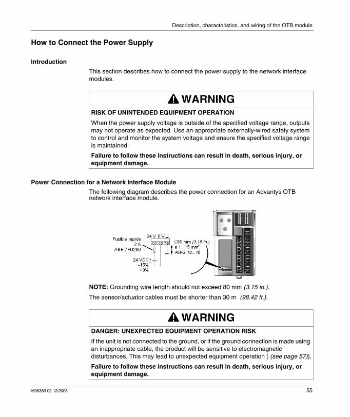
Power Connection for a Network Interface Module
The following diagram describes the power connection for an Advantys OTB network interface module.
NOTE: Grounding wire length should not exceed 80 mm (3.15 in.).
The sensor/actuator cables must be shorter than 30 m (98.42 ft.).
WARNINGRISK OF UNINTENDED EQUIPMENT OPERATION
When the power supply voltage is outside of the specified voltage range, outputs may not operate as expected. Use an appropriate externally-wired safety system to control and monitor the system voltage and ensure the specified voltage range is maintained.
Failure to follow these instructions can result in death, serious injury, or equipment damage.
WARNINGDANGER: UNEXPECTED EQUIPMENT OPERATION RISK
If the unit is not connected to the ground, or if the ground connection is made using an inappropriate cable, the product will be sensitive to electromagnetic disturbances. This may lead to unexpected equipment operation ( (see page 57)).
Failure to follow these instructions can result in death, serious injury, or equipment damage.
1606383 02 12/2008 55

Description, characteristics, and wiring of the OTB module
Network Interface Module Power Supply Specifications
The following table describes the power supply specifications for the network interface module.
NOTE: Momentary power interruption for 10 ms or less at 24 VDC is not recognized as failure.
Item Characteristics
Power supply voltage
Rated power voltage: 24 VDCAllowable range: from 20.4 to 26.4 VDC
Inrush current flow atpower-up
50 A maximum
Power supply wiring
0.14 mm2 (AWG26) or 1.5 mm2 (AWG16)Make the power supply wiring as short as possible.
Ground wiring 1 mm2 (AWG18) or 1.5 mm2 (AWG16)Do not connect ground wire in common with ground wire of motor equip-ment.The grounding connection should be as short as possible < 8 cm (3.15 in).
56 1606383 02 12/2008

Description, characteristics, and wiring of the OTB module
EMC Compatibility
Product Compliance
This product complies with the European directive 89/336/EEC on "electromagnetic compatibility".
The products described in this manual meet all the conditions regarding electromagnetic compatibility and are compliant with the applicable standards. However, this does not mean that the electromagnetic compatibility of your installation is assured.
This is why it is strongly recommended to follow all instructions concerning an EMC-compliant installation. Only in these conditions and thanks to the exclusive use of CE approved components, will the devices used be deemed to comply with the EMC directives.
When handling the products, ensure that all safety measures related to electromagnetic compatibility and all conditions for the use of the products are complied with by all persons concerned. This is especially important when handling products sensitive to electrostatic discharges.
WARNINGRISK OF ELECTROMAGNETIC INTERFERENCE AND UNINTENDED EQUIP-MENT OPERATION
The products described in this manual contain highly complex semiconductors that can be damaged or destroyed by electrostatic discharges (ESD). If, for example, they are used within the vicinity of devices rated as class A or B according to IEC 6100-4-4, the level of electromagnetic interference may be enough to cause the device to operate unexpectedly, and/or to damage it.
Damage may not necessarily cause a failure or malfunction that is immediately detectable. It may occur sporadically or in a delayed manner.
If there is a risk of electromagnetic interference, the system designer must implement the necessary protective measures.
Failure to follow these instructions can result in death, serious injury, or equipment damage.
1606383 02 12/2008 57
Description, characteristics, and wiring of the OTB module
Grounding
The grounding cable must be shorter than 8 cm (0.262 ft).
Cable Routing
Make sure that the following basic wiring rules are observed:
Make sure there is a space of at least 10 cm (3.94 inches) between the data cables and the power cables.The data cables and power cables must only cross at a right angle to one another.It is advisable to route the data cables and power cables through separate shielded ducts.When laying the cables, the noise voltage from other devices or wires must be considered. This particularly applies to frequency converters, motors and other devices or cables generating high frequency disturbance. High-frequency sources and the cables described in this manual must be as far apart from each other as possible.
WARNINGRISK OF UNINTENDED EQUIPMENT OPERATION
If the unit is not connected to the ground, or if the ground connection is made using an inappropriate cable, the product will be sensitive to electromagnetic disturbance. This can lead to unintended equipment operation.
Failure to follow these instructions can result in death, serious injury, or equipment damage.
WARNINGRISK OF UNINTENDED EQUIPMENT OPERATION
Please read and comply with the cabling rules listed above. Failure to comply with these wiring rules is a common cause of EMC problems! This can lead to unintended equipment operation.
Failure to follow these instructions can result in death, serious injury, or equipment damage.
58 1606383 02 12/2008

Description, characteristics, and wiring of the OTB module
Control of Inductive Loads
The outputs of the devices described in this manual are equipped with an integrated protective system against the high noise voltages that may be generated by inductive loads.
Integrated protective system against the high noise voltages generated by inductive loads
The varistor rapidly discharges the energy accumulated in the magnetic field of the inductive load.
The high voltages arising from the disconnection of inductive loads create large fields in the wires that may cause disturbances in nearby circuits or devices. It is advisable to fit an anti-interference device on the load. In this way, the voltage peak generated by the inductive load is short-circuited directly at the point where it occurs.
1606383 02 12/2008 59
Description, characteristics, and wiring of the OTB module
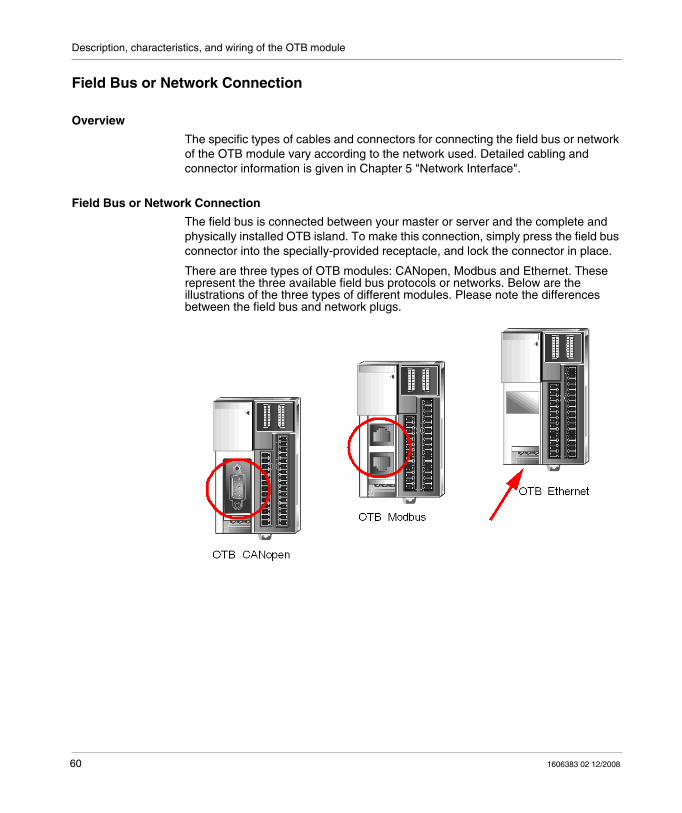
Field Bus or Network Connection
Overview
The specific types of cables and connectors for connecting the field bus or network of the OTB module vary according to the network used. Detailed cabling and connector information is given in Chapter 5 "Network Interface".
Field Bus or Network Connection
The field bus is connected between your master or server and the complete and physically installed OTB island. To make this connection, simply press the field bus connector into the specially-provided receptacle, and lock the connector in place.
There are three types of OTB modules: CANopen, Modbus and Ethernet. These represent the three available field bus protocols or networks. Below are the illustrations of the three types of different modules. Please note the differences between the field bus and network plugs.
60 1606383 02 12/2008
1606383 02 12/2008
4
Description, characteristics, and wiring of the expansion modules
1606383 02 12/2008
Description, characteristics, and wiring of the expansion modules
Introduction
This chapter provides an overview of the analog and Discrete I/O expansion modules. Information on functions and wiring is given for each expansion module.
What's in this Chapter?
This chapter contains the following sections:
Section Topic Page
4.1 Discrete Expansion Modules 62
4.2 Analog Expansion Modules 63
4.3 Expansion Module Common Blocks 64
61

Description, characteristics, and wiring of the expansion modules
4.1 Discrete Expansion Modules
Discrete Expansion Modules
Reference Documents
Refer to the hardware installation manual for TM2 discrete I/O modules.
62 1606383 02 12/2008

Description, characteristics, and wiring of the expansion modules
4.2 Analog Expansion Modules
Analog Expansion Modules
Reference Documents
Refer to the hardware installation manual for TM2 analog I/O modules.
1606383 02 12/2008 63
Description, characteristics, and wiring of the expansion modules
4.3 Expansion Module Common Blocks
Common Block Expansion Module Wiring Diagrams
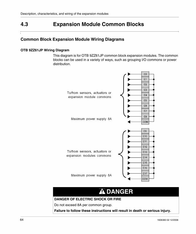
OTB 9ZZ61JP Wiring Diagram
This diagram is for OTB 9ZZ61JP common block expansion modules. The common blocks can be used in a variety of ways, such as grouping I/O commons or power distribution.
DANGERDANGER OF ELECTRIC SHOCK OR FIRE
Do not exceed 8A per common group.
Failure to follow these instructions will result in death or serious injury.
64 1606383 02 12/2008
1606383 02 12/2008
5
Modbus Network Interface of the OTB Module
1606383 02 12/2008
Modbus Network Interface of the OTB Module
Introduction
This chapter describes the external Modbus characteristics of the Advantys OTB network interface module and the general Modbus features supported by the module.
What's in this Chapter?
This chapter contains the following sections:
Section Topic Page
5.1 General Principles 66
5.2 Cabling on the Modbus Network 69
5.3 Behavior of OTB Modbus Splitter Box 79
65
Modbus Network Interface of the OTB Module
5.1 General Principles
Communication on the Modbus Network
Introduction
The Modbus protocol is a master-slave protocol that allows one, and only one, master to request responses from slaves, or to act on the basis of the request. The master can address individual slaves, or can send a broadcast message to all slaves. Slaves return a message (response) to requests that are addressed to them individually. Responses are not returned to broadcast requests from the master.
Modbus Message Structure
The Modbus protocol uses 16-bit words (registers) divided into two bytes of 8 bits. A Modbus message starts with a header followed by a 1-byte address. A Modbus message uses a Modbus function code (see page 67) as its first byte.
The table below describes the full structure of a Modbus RTU message:
NOTE: For further information on the message structure, please refer to the documentation for your Modbus master.
WARNINGRISK OF UNINTENDED EQUIPMENT OPERATION
Do not use more than one master on the Modbus network. Unexpected I/O behavior can result if more than one master is able to communicate on the network at the same time.
Depending on the I/O configuration, unexpected equipment operation can result if more than one master is in use.
Failure to follow these instructions can result in death, serious injury, or equipment damage.
Modbus Messages
Address Function code Data CRC
one byte one byte n-byte field two bytes
66 1606383 02 12/2008
Modbus Network Interface of the OTB Module
List of Supported Commands
The table below lists the Modbus commands supported by the OTB module:
NOTE: Registers can be read or written if and only if the registers are adjacent.
Reading n registers (03):
This function code is used to read the content of one or more adjacent registers in a slave.
Writing a register (06):
This function code is used to write the content of a register in a slave.
Writing n registers (16):
This function code is used to write the content of one or more contiguous registers in a slave.
Mask writing (22):
This function code is used to modify the content (in whole or part) of a register. This function is a combination of an AND mask, an OR mask, an AND NOT mask and the current content of the register.
Example:
Reading/Writing n registers (23):
This function code is used to execute a combination of reading and writing n registers.
Identification (43 sub-index 14):
This function code is used to read the identification and other information relating to the physical description of a slave.
Modbus Function Code:Dec Index (Hex)
Sub-Function: Sub-Index
Command
3 (0003H) Read n registers
6 (0006H) Write a single register
16 (0010H) Write n registers
22 (0016H) Mask write register
23 (0017H) Read/Write n registers
43 (002BH) 14 Read slave identification registers
Hexadecimal Binary
Current content 18 (12H) 0001 0010
AND mask 242 (F2H) 1111 0010
OR mask 37 (25H) 0010 0101
AND NOT mask 13 (0DH) 0000 1101
Result 23 (17H) 0001 0111
1606383 02 12/2008 67
Modbus Network Interface of the OTB Module
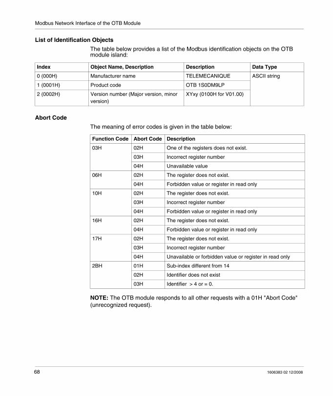
List of Identification Objects
The table below provides a list of the Modbus identification objects on the OTB module island:
Abort Code
The meaning of error codes is given in the table below:
NOTE: The OTB module responds to all other requests with a 01H "Abort Code" (unrecognized request).
Index Object Name, Description Description Data Type
0 (000H) Manufacturer name TELEMECANIQUE ASCII string
1 (0001H) Product code OTB 1S0DM9LP
2 (0002H) Version number (Major version, minor version)
XYxy (0100H for V01.00)
Function Code Abort Code Description
03H 02H One of the registers does not exist.
03H Incorrect register number
04H Unavailable value
06H 02H The register does not exist.
04H Forbidden value or register in read only
10H 02H The register does not exist.
03H Incorrect register number
04H Forbidden value or register in read only
16H 02H The register does not exist.
04H Forbidden value or register in read only
17H 02H The register does not exist.
03H Incorrect register number
04H Unavailable or forbidden value or register in read only
2BH 01H Sub-index different from 14
02H Identifier does not exist
03H Identifier > 4 or = 0.
68 1606383 02 12/2008

Modbus Network Interface of the OTB Module
5.2 Cabling on the Modbus Network
Introduction
This section describes cabling on the Modbus network.
What's in this Section?
This section contains the following topics:
Topic Page
Description of the OTB Module Modbus Network Interface 70
Modbus Field Bus Interface 71
Network Node Address 74
Network Speed 76
Modbus Configuration 78
1606383 02 12/2008 69
Modbus Network Interface of the OTB Module
Description of the OTB Module Modbus Network Interface
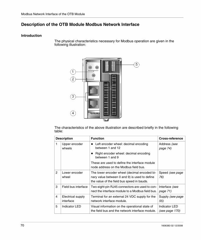
Introduction
The physical characteristics necessary for Modbus operation are given in the following illustration:
The characteristics of the above illustration are described briefly in the following table:
Description Function Cross-reference
1 Upper encoder wheels
Left encoder wheel: decimal encoding between 1 and 12
Right encoder wheel: decimal encoding between 1 and 9
These are used to define the interface module node address on the Modbus field bus.
Address (see page 74)
2 Lower encoder wheel
The lower encoder wheel (decimal encoded bi-nary value between 0 and 9) is used to define the value of the field bus speed in bauds.
Speed (see page 76)
3 Field bus interface Two eight-pin RJ45 connectors are used to con-nect the interface module to a Modbus field bus.
Interface (see page 71)
4 Electrical supply interface
Terminal for an external 24 VDC supply for the network interface module.
Supply (see page 55)
5 Indicator LED Visual information on the operational state of the field bus and the network interface module.
Indicator LED (see page 170)
70 1606383 02 12/2008
Modbus Network Interface of the OTB Module
Modbus Field Bus Interface
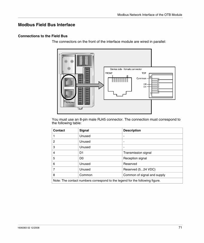
Connections to the Field Bus
The connectors on the front of the interface module are wired in parallel:
You must use an 8-pin male RJ45 connector. The connection must correspond to the following table:
Contact Signal Description
1 Unused -
2 Unused -
3 Unused -
4 D1 Transmission signal
5 D0 Reception signal
6 Unused Reserved
7 Unused Reserved (5...24 VDC)
8 Common Common of signal and supply
Note: The contact numbers correspond to the legend for the following figure.
1606383 02 12/2008 71
Modbus Network Interface of the OTB Module
Correspondence of Pin Assignments
Advantys OTB network interface modules can be connected with other Schneider products over Modbus. These products have different pin assignments but all are standard RS 485 compliant.
The table below shows the correspondence between product and pin names:
Modbus Network Connectors and Cables
The branch cable between the field bus and the island must have a female connector complying with the preceding pin assignment diagram. The Modbus network cable is a standard RS 485 compliant shielded twisted pair cable and the shielding must be grounded.
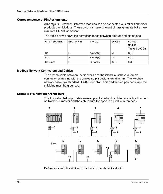
Example of a Network Architecture
The illustration below provides an example of a network architecture with a Premium or Twido bus master and the cables with the specified product references.
References and description of numbers in the above illustration
OTB 1S0DM9LP EIA/TIA 485 TWIDO SCA64 SCA62SCA50Tesys LU9CG3
D1 B A or A(+) M+ D(B)
D0 A B or B(+) M- D(A)
Common C SG or 0V 0VL 0VL
72 1606383 02 12/2008
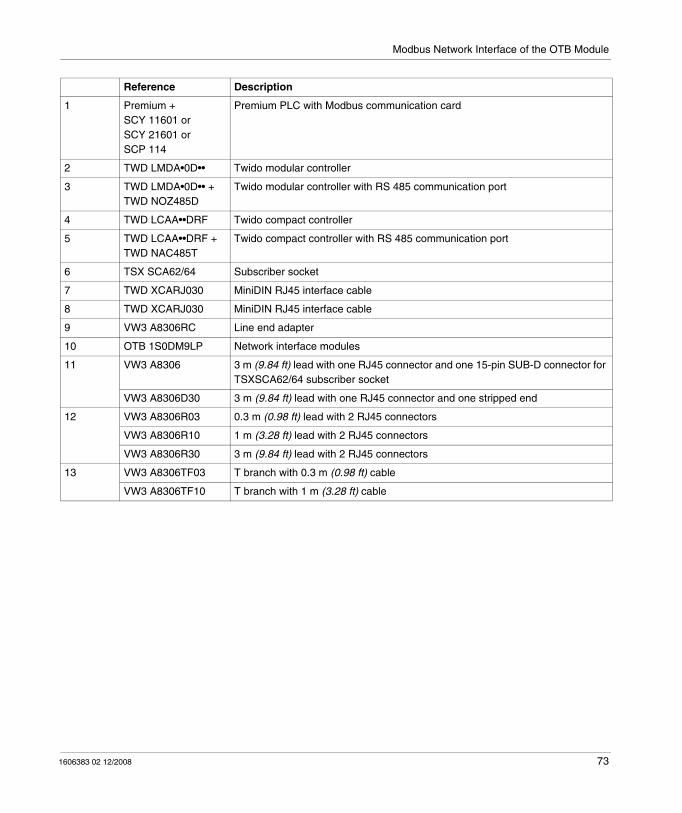
Modbus Network Interface of the OTB Module
Reference Description
1 Premium +SCY 11601 or SCY 21601 or SCP 114
Premium PLC with Modbus communication card
2 TWD LMDA•0D•• Twido modular controller
3 TWD LMDA•0D•• + TWD NOZ485D
Twido modular controller with RS 485 communication port
4 TWD LCAA••DRF Twido compact controller
5 TWD LCAA••DRF + TWD NAC485T
Twido compact controller with RS 485 communication port
6 TSX SCA62/64 Subscriber socket
7 TWD XCARJ030 MiniDIN RJ45 interface cable
8 TWD XCARJ030 MiniDIN RJ45 interface cable
9 VW3 A8306RC Line end adapter
10 OTB 1S0DM9LP Network interface modules
11 VW3 A8306 3 m (9.84 ft) lead with one RJ45 connector and one 15-pin SUB-D connector for TSXSCA62/64 subscriber socket
VW3 A8306D30 3 m (9.84 ft) lead with one RJ45 connector and one stripped end
12 VW3 A8306R03 0.3 m (0.98 ft) lead with 2 RJ45 connectors
VW3 A8306R10 1 m (3.28 ft) lead with 2 RJ45 connectors
VW3 A8306R30 3 m (9.84 ft) lead with 2 RJ45 connectors
13 VW3 A8306TF03 T branch with 0.3 m (0.98 ft) cable
VW3 A8306TF10 T branch with 1 m (3.28 ft) cable
1606383 02 12/2008 73
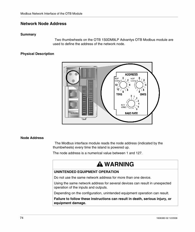
Modbus Network Interface of the OTB Module
Network Node Address
Summary
Two thumbwheels on the OTB 1S0DM9LP Advantys OTB Modbus module are used to define the address of the network node.
Physical Description
Node Address
The Modbus interface module reads the node address (indicated by the thumbwheels) every time the island is powered up.
The node address is a numerical value between 1 and 127.
WARNINGUNINTENDED EQUIPMENT OPERATION
Do not use the same network address for more than one device.
Using the same network address for several devices can result in unexpected operation of the inputs and outputs.
Depending on the configuration, unintended equipment operation can result.
Failure to follow these instructions can result in death, serious injury, or equipment damage.
74 1606383 02 12/2008
Modbus Network Interface of the OTB Module
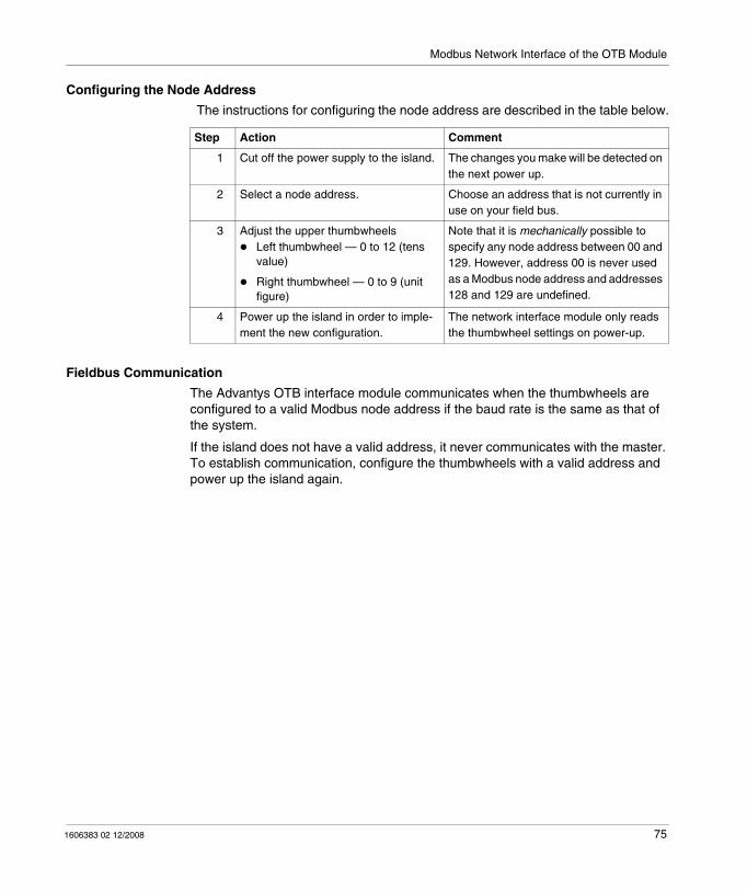
Configuring the Node Address
The instructions for configuring the node address are described in the table below.
Fieldbus Communication
The Advantys OTB interface module communicates when the thumbwheels are configured to a valid Modbus node address if the baud rate is the same as that of the system.
If the island does not have a valid address, it never communicates with the master. To establish communication, configure the thumbwheels with a valid address and power up the island again.
Step Action Comment
1 Cut off the power supply to the island. The changes you make will be detected on the next power up.
2 Select a node address. Choose an address that is not currently in use on your field bus.
3 Adjust the upper thumbwheels Left thumbwheel — 0 to 12 (tens value)
Right thumbwheel — 0 to 9 (unit figure)
Note that it is mechanically possible to specify any node address between 00 and 129. However, address 00 is never used as a Modbus node address and addresses 128 and 129 are undefined.
4 Power up the island in order to imple-ment the new configuration.
The network interface module only reads the thumbwheel settings on power-up.
1606383 02 12/2008 75
Modbus Network Interface of the OTB Module
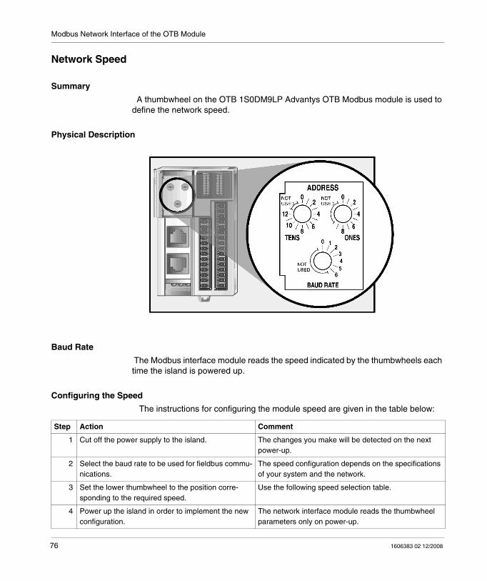
Network Speed
Summary
A thumbwheel on the OTB 1S0DM9LP Advantys OTB Modbus module is used to define the network speed.
Physical Description
Baud Rate
The Modbus interface module reads the speed indicated by the thumbwheels each time the island is powered up.
Configuring the Speed
The instructions for configuring the module speed are given in the table below:
Step Action Comment
1 Cut off the power supply to the island. The changes you make will be detected on the next power-up.
2 Select the baud rate to be used for fieldbus commu-nications.
The speed configuration depends on the specifications of your system and the network.
3 Set the lower thumbwheel to the position corre-sponding to the required speed.
Use the following speed selection table.
4 Power up the island in order to implement the new configuration.
The network interface module reads the thumbwheel parameters only on power-up.
76 1606383 02 12/2008

Modbus Network Interface of the OTB Module
Speed Selection Table
.
Position (Lower Thumbwheel)
Baud Rate
0 19200 bps (default)
1 1200 bps
2 2400 bps
3 4800 bps
4 9600 bps
5 19200 bps
6 38400 bps
1606383 02 12/2008 77
Modbus Network Interface of the OTB Module
Modbus Configuration
Electrical Specifications
The network interface module supports 2-wire Modbus. Communication type is half-duplex.
Communications Configuration
The Modbus communication parameters which define the frame can be configured in a number of different ways.
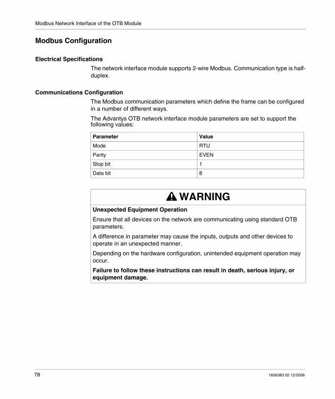
The Advantys OTB network interface module parameters are set to support the following values:
Parameter Value
Mode RTU
Parity EVEN
Stop bit 1
Data bit 8
WARNINGUnexpected Equipment Operation
Ensure that all devices on the network are communicating using standard OTB parameters.
A difference in parameter may cause the inputs, outputs and other devices to operate in an unexpected manner.
Depending on the hardware configuration, unintended equipment operation may occur.
Failure to follow these instructions can result in death, serious injury, or equipment damage.
78 1606383 02 12/2008

Modbus Network Interface of the OTB Module
5.3 Behavior of OTB Modbus Splitter Box
1606383 02 12/2008 79
Modbus Network Interface of the OTB Module
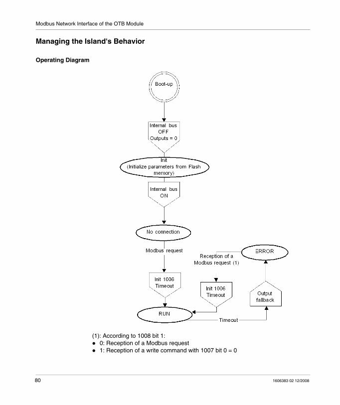
Managing the Island's Behavior
Operating Diagram
(1): According to 1008 bit 1:0: Reception of a Modbus request1: Reception of a write command with 1007 bit 0 = 0
80 1606383 02 12/2008
Modbus Network Interface of the OTB Module
Setting the Analog Expansion Module Parameters
To set the analog expansion module parameters, you must stop activity on the island's internal bus by writing the value 1 to the register 1005.
Once the expansion module configuration parameters have been updated, the content of register 1005 must be reset to 0 to restart activity on the internal bus with the new parameters.
NOTE: If a non-compliant parameter is sent, register 1005 cannot be written to zero.
32-Bit Function and Fault Acknowledgement Mode
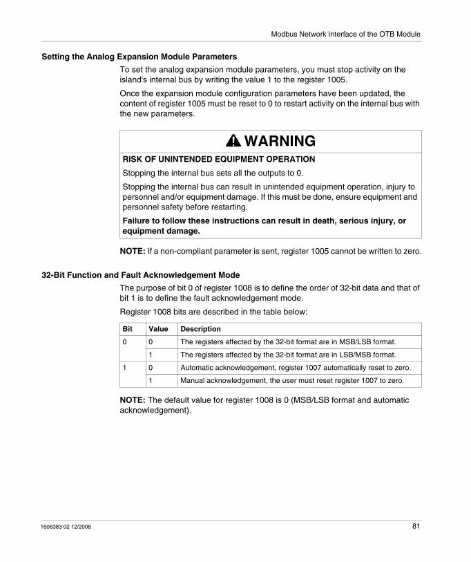
The purpose of bit 0 of register 1008 is to define the order of 32-bit data and that of bit 1 is to define the fault acknowledgement mode.
Register 1008 bits are described in the table below:
NOTE: The default value for register 1008 is 0 (MSB/LSB format and automatic acknowledgement).
WARNINGRISK OF UNINTENDED EQUIPMENT OPERATION
Stopping the internal bus sets all the outputs to 0.
Stopping the internal bus can result in unintended equipment operation, injury to personnel and/or equipment damage. If this must be done, ensure equipment and personnel safety before restarting.
Failure to follow these instructions can result in death, serious injury, or equipment damage.
Bit Value Description
0 0 The registers affected by the 32-bit format are in MSB/LSB format.
1 The registers affected by the 32-bit format are in LSB/MSB format.
1 0 Automatic acknowledgement, register 1007 automatically reset to zero.
1 Manual acknowledgement, the user must reset register 1007 to zero.
1606383 02 12/2008 81
Modbus Network Interface of the OTB Module
Fault Acknowledgement
Register 1007 is used to manage fault acknowledgement. This register manages different read and write data.
WRITE access for register 1007:
NOTE: Bits 2...15 are ignored and must be written to 0, writing the value 1 will have no effect.
READ access for register 1007 (automatically updated by the OTB):
Fault Counter
Register 1009 is used to count the number of network monitoring faults; this register is only accessible in read mode.
Setting the Network Monitoring Time
Register 1006 is used to set the OTB module monitoring time in ms.
Values for register 1006 0: no network monitoring (default value)x: monitoring time in ms (x: = 1 to 65535 ms)
NOTE: Do not enter values lower than the client's read cycle.
Network Monitoring
The island goes into fallback mode if no frame is detected on the network before the monitoring time expires. All island outputs and special functions change to the fallback values defined by the user.
Bit 9 of register 900 changes to 1 indicating that the OTB module has changed to fallback mode.
Writing the value 0 to the command register 1007 enables you to set bit 9 of register 900 to zero in order to restart network monitoring.
Bit 1 Bit 0 Description Decimal Value
0 0 Fault acknowledgement without default counter reset to zero (register 1009)
0
1 0 Fault acknowledgement and default counter reset to zero (register 1009 = 0)
2
1 1 Fault counter reset to zero (register 1009 = 0) without fault acknowledgement
3
Bits 15...1 Bit 0 Description
Reserved 0 No fault
Reserved 1 Fault present
82 1606383 02 12/2008
Modbus Network Interface of the OTB Module
Saving and Restoring Parameters
Initialization
An OTB module is initialized with default parameters. When detected by the bus master, the OTB module is configured with the user-defined parameters sent by the master. These parameters must be saved so that they can be taken into account the next time the system is started.
Current parameters
Register 1000 indicates the current set of parameters:0: The island is using the default parameter set (factory settings)1: The island is using the set of saved parameters2: One or more parameters have been modified since the last save or last start-up where the flash memory content was erased following a restoration command.
Saving parameters
The parameters are saved by replacing the value in register 1002 with a different value.
This saves the current parameters of the OTB module and tells it to use these saved parameters on future start-ups.
A backup counter is available in register 1001. This counter is reset to 0 when the factory settings are restored.
NOTE: The saved registers correspond to the parameter registers for the different zones (registers 200 to 899 and 1000 to 1099).
When saving is in progress, the module stops communication for 300 ms.
WARNINGRISK OF UNINTENDED EQUIPMENT OPERATION
Do not save or restore configuration parameters during normal equipment operation. Saving or restoring the parameters will halt communications and turn off the expansion module outputs. Depending on the I/O configuration, this may result in unintended equipment operation.
Failure to follow these instructions can result in death, serious injury, or equipment damage.
1606383 02 12/2008 83
Modbus Network Interface of the OTB Module
Restoring Parameters
The different possible restore operations are described in the following table:
NOTE:
The registers must be modified to a value other than their current value.When restoring the factory settings (1004), the client configuration is lost.
Identifying the Island Modules
The table below describes the mapping of modules on the island.
NOTE: (1) The register code depends on the type of connected expansion module. See the register code for each type of expansion module in the table below. The default value is equal to FFFFH.
To restore... you should modify the value in register...
the last saved configuration 1003
the factory settings 1004
Registers Functions Register Code
1100 OTB product code FEFDH
1101 OTB software version XYxy
1102 Type of expansion module 1 (1)
1103 Type of expansion module 2 (1)
1104 Type of expansion module 3 (1)
1105 Type of expansion module 4 (1)
1106 Type of expansion module 5 (1)
1107 Type of expansion module 6 (1)
1108 Type of expansion module 7 (1)
84 1606383 02 12/2008
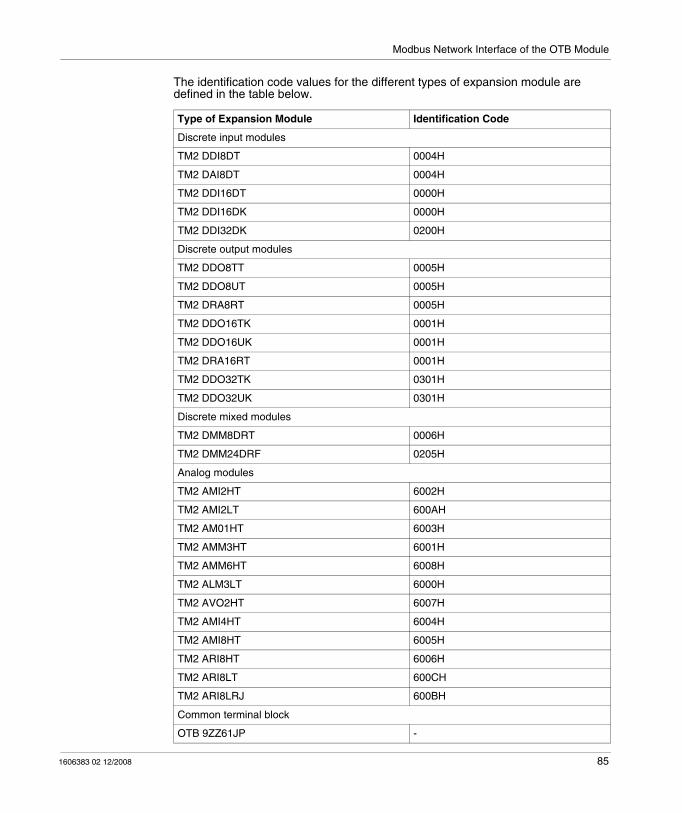
Modbus Network Interface of the OTB Module
The identification code values for the different types of expansion module are defined in the table below.
Type of Expansion Module Identification Code
Discrete input modules
TM2 DDI8DT 0004H
TM2 DAI8DT 0004H
TM2 DDI16DT 0000H
TM2 DDI16DK 0000H
TM2 DDI32DK 0200H
Discrete output modules
TM2 DDO8TT 0005H
TM2 DDO8UT 0005H
TM2 DRA8RT 0005H
TM2 DDO16TK 0001H
TM2 DDO16UK 0001H
TM2 DRA16RT 0001H
TM2 DDO32TK 0301H
TM2 DDO32UK 0301H
Discrete mixed modules
TM2 DMM8DRT 0006H
TM2 DMM24DRF 0205H
Analog modules
TM2 AMI2HT 6002H
TM2 AMI2LT 600AH
TM2 AM01HT 6003H
TM2 AMM3HT 6001H
TM2 AMM6HT 6008H
TM2 ALM3LT 6000H
TM2 AVO2HT 6007H
TM2 AMI4HT 6004H
TM2 AMI8HT 6005H
TM2 ARI8HT 6006H
TM2 ARI8LT 600CH
TM2 ARI8LRJ 600BH
Common terminal block
OTB 9ZZ61JP -
1606383 02 12/2008 85

Modbus Network Interface of the OTB Module
86 1606383 02 12/2008
1606383 02 12/2008
6
Application-Specific Functions
1606383 02 12/2008
Application-Specific Functions
Introduction
This section describes the application-specific functions of the Advantys OTB modules. The information concerning I/O assignments, configuration and usage are provided for the OTB module and each expansion module.
What's in this Chapter?
This chapter contains the following sections:
Section Topic Page
6.1 Island Registers 88
6.2 Description of the OTB Module I/Os 92
6.3 Specific Functions of the OTB Module 97
6.4 Discrete I/O of Expansion Modules 125
6.5 Analog I/O of Expansion Modules 129
87
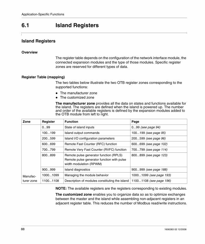
Application-Specific Functions
6.1 Island Registers
Island Registers
Overview
The register table depends on the configuration of the network interface module, the connected expansion modules and the type of those modules. Specific register zones are reserved for different types of data.
Register Table (mapping)
The two tables below illustrate the two OTB register zones corresponding to the supported functions:
The manufacturer zoneThe customized zone
The manufacturer zone provides all the data on states and functions available for the island. The registers are defined when the island is powered up. The number and order of the available registers is defined by the expansion modules added to the OTB module from left to right.
NOTE: The available registers are the registers corresponding to existing modules.
The customized zone enables you to organize data so as to optimize exchanges between the master and the island while assembling non-adjacent registers in an adjacent register table. This reduces the number of Modbus read/write instructions.
Zone Register Function Page
Manufac-turer zone
0...99 State of island inputs 0...99 (see page 94)
100...199 Island output commands 100...199 (see page 95)
200...599 Island I/O configuration parameters 200...599 (see page 96)
600...699 Remote Fast Counter (RFC) function 600...699 (see page 102)
700...799 Remote Very Fast Counter (RVFC) function 700...799 (see page 114)
800...899 Remote pulse generator function (RPLS)Remote pulse generator function with pulse width modulation (RPWM)
800...899 (see page 123)
900...999 Island diagnostics 900...999 (see page 188)
1000...1099 Managing the module behavior 1000...1099 (see page 193)
1100...1108 Description of modules constituting the island 1100...1108 (see page 196)
88 1606383 02 12/2008
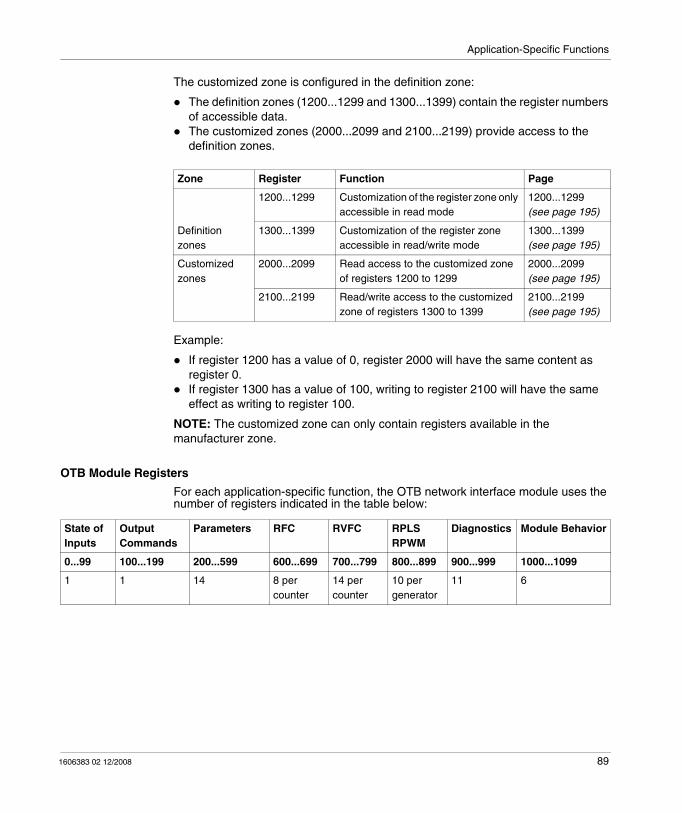
Application-Specific Functions
The customized zone is configured in the definition zone:
The definition zones (1200...1299 and 1300...1399) contain the register numbers of accessible data.The customized zones (2000...2099 and 2100...2199) provide access to the definition zones.
Example:
If register 1200 has a value of 0, register 2000 will have the same content as register 0.If register 1300 has a value of 100, writing to register 2100 will have the same effect as writing to register 100.
NOTE: The customized zone can only contain registers available in the manufacturer zone.
OTB Module Registers
For each application-specific function, the OTB network interface module uses the number of registers indicated in the table below:
Zone Register Function Page
Definition zones
1200...1299 Customization of the register zone only accessible in read mode
1200...1299 (see page 195)
1300...1399 Customization of the register zone accessible in read/write mode
1300...1399 (see page 195)
Customized zones
2000...2099 Read access to the customized zone of registers 1200 to 1299
2000...2099 (see page 195)
2100...2199 Read/write access to the customized zone of registers 1300 to 1399
2100...2199 (see page 195)
State of Inputs
Output Commands
Parameters RFC RVFC RPLSRPWM
Diagnostics Module Behavior
0...99 100...199 200...599 600...699 700...799 800...899 900...999 1000...1099
1 1 14 8 per counter
14 per counter
10 per generator
11 6
1606383 02 12/2008 89
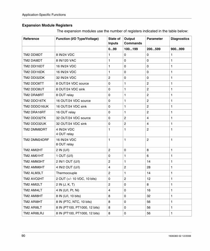
Application-Specific Functions
Expansion Module Registers
The expansion modules use the number of registers indicated in the table below:
Reference Function (I/O Type/Voltage) State of Inputs
Output Commands
Parameter Diagnostics
0...99 100...199 200...599 900...999
TM2 DDI8DT 8 IN/24 VDC 1 0 0 1
TM2 DAI8DT 8 IN/120 VAC 1 0 0 1
TM2 DDI16DT 16 IN/24 VDC 1 0 0 1
TM2 DDI16DK 16 IN/24 VDC 1 0 0 1
TM2 DDI32DK 32 IN/24 VDC 2 0 0 1
TM2 DDO8TT 8 OUT/24 VDC source 0 1 2 1
TM2 DDO8UT 8 OUT/24 VDC sink 0 1 2 1
TM2 DRA8RT 8 OUT relay 0 1 2 1
TM2 DDO16TK 16 OUT/24 VDC source 0 1 2 1
TM2 DDDO16UK 16 OUT/24 VDC sink 0 1 2 1
TM2 DRA16RT 16 OUT relay 0 1 2 1
TM2 DDO32TK 32 OUT/24 VDC source 0 2 4 1
TM2 DDO32UK 32 OUT/24 VDC sink 0 2 4 1
TM2 DMM8DRT 4 IN/24 VDC4 OUT relay
1 1 2 1
TM2 DMM24DRF 16 IN/24 VDC8 OUT relay
1 1 2 1
TM2 AMI2HT 2 IN (U/I) 2 0 8 1
TM2 AM01HT 1 OUT (U/I) 0 1 6 1
TM2 AMM3HT 2 IN/1 OUT (U/I) 2 1 14 1
TM2 AMM6HT 4 IN/2 OUT (U/I) 4 2 28 1
TM2 ALM3LT Thermocouple 2 1 14 1
TM2 AVO2HT 2 OUT (+/- 10 VDC, 10 bits) 0 2 12 1
TM2 AMI2LT 2 IN (J, K, T) 2 0 8 1
TM2 AMI4LT 4 IN (U/I, Pt, Ni) 4 0 16 1
TM2 AMI8HT 8 IN (U/I, 10 bits) 8 0 32 1
TM2 ARI8HT 8 IN (PTC, NTC, 10 bits) 8 0 56 1
TM2 ARI8LT 8 IN (PT100, PT1000, 12 bits) 8 0 56 1
TM2 ARI8LRJ 8 IN (PT100, PT1000, 12 bits) 8 0 56 1
90 1606383 02 12/2008
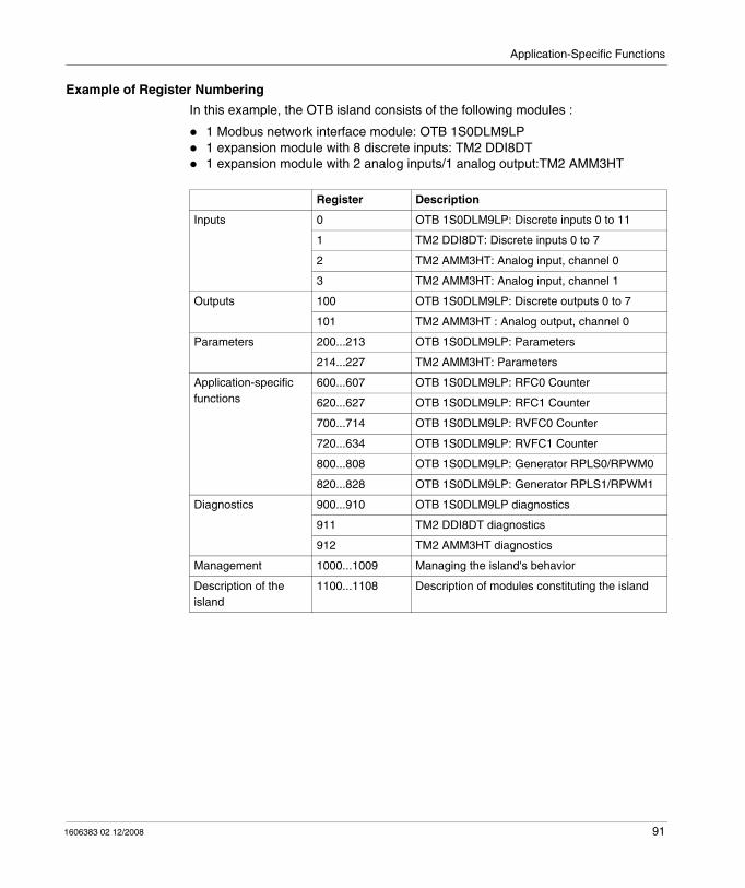
Application-Specific Functions
Example of Register Numbering
In this example, the OTB island consists of the following modules :
1 Modbus network interface module: OTB 1S0DLM9LP 1 expansion module with 8 discrete inputs: TM2 DDI8DT1 expansion module with 2 analog inputs/1 analog output:TM2 AMM3HT
Register Description
Inputs 0 OTB 1S0DLM9LP: Discrete inputs 0 to 11
1 TM2 DDI8DT: Discrete inputs 0 to 7
2 TM2 AMM3HT: Analog input, channel 0
3 TM2 AMM3HT: Analog input, channel 1
Outputs 100 OTB 1S0DLM9LP: Discrete outputs 0 to 7
101 TM2 AMM3HT : Analog output, channel 0
Parameters 200...213 OTB 1S0DLM9LP: Parameters
214...227 TM2 AMM3HT: Parameters
Application-specific functions
600...607 OTB 1S0DLM9LP: RFC0 Counter
620...627 OTB 1S0DLM9LP: RFC1 Counter
700...714 OTB 1S0DLM9LP: RVFC0 Counter
720...634 OTB 1S0DLM9LP: RVFC1 Counter
800...808 OTB 1S0DLM9LP: Generator RPLS0/RPWM0
820...828 OTB 1S0DLM9LP: Generator RPLS1/RPWM1
Diagnostics 900...910 OTB 1S0DLM9LP diagnostics
911 TM2 DDI8DT diagnostics
912 TM2 AMM3HT diagnostics
Management 1000...1009 Managing the island's behavior
Description of the island
1100...1108 Description of modules constituting the island
1606383 02 12/2008 91

Application-Specific Functions
6.2 Description of the OTB Module I/Os
Introduction
This section presents the I/O of the OTB module.
What's in this Section?
This section contains the following topics:
Topic Page
Description of the OTB Module Discrete I/Os 93
Read Input Registers 94
Output Command Registers 95
Advantys OTB Module I/O Parameter Registers 96
92 1606383 02 12/2008
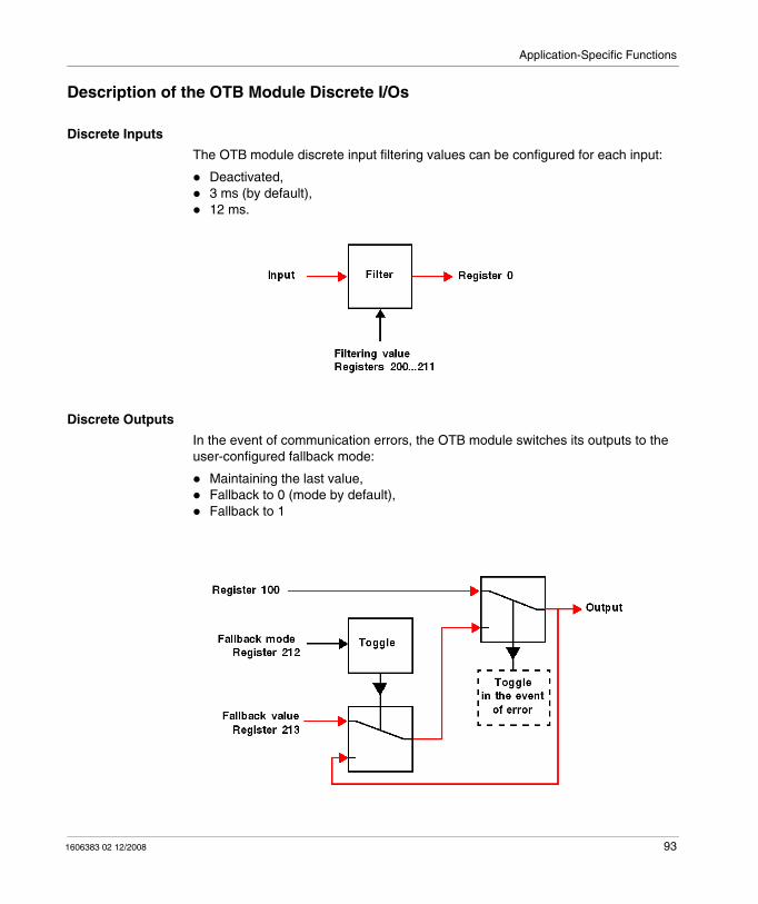
Application-Specific Functions
Description of the OTB Module Discrete I/Os
Discrete Inputs
The OTB module discrete input filtering values can be configured for each input:
Deactivated,3 ms (by default),12 ms.
Discrete Outputs
In the event of communication errors, the OTB module switches its outputs to the user-configured fallback mode:
Maintaining the last value,Fallback to 0 (mode by default),Fallback to 1
1606383 02 12/2008 93
Application-Specific Functions
Read Input Registers
At a Glance
This section describes how to read the status of the Advantys OTB island inputs.
Discrete inputs of expansion modules are not filtered.
NOTE: The order of the parameters is defined by expansion modules added to the OTB module from left to right. The number of parameters depends on the number and type of expansion modules connected.
Table of Read Input Registers 0 to 99
The following table gives the bit assignment for each of the read input registers:
NOTE: Only those registers that correspond to an expansion module present in the island are accessible in read mode.
Register Function Bit assignment
0 Status of Advantys OTB module inputs Bit 0: Input 0...Bit 11: Input 11Bits 12 to 15: Not used
1 Input status of first expansion module with inputs Depends on the module
... ... ...
99 ... ...
94 1606383 02 12/2008
Application-Specific Functions
Output Command Registers
At a Glance
This section describes how to write to Advantys OTB island outputs.
NOTE: The order of the parameters is defined by expansion modules added to the OTB module from left to right. The number of parameters depends on the number and type of expansion modules connected.
Table of Output Command Registers 100 to 199
The following table gives the bit assignment for each of the write output registers:
NOTE: Only those registers that correspond to an expansion module present in the island are readable and writeable.
Register Function Bit assignment
100 Advantys OTB module output commands Bit 0: Output 0...Bit 11: Output 11
101 Commands to outputs of first expansion module with outputs
Depends on the module
... ... ...
199 ... ...
1606383 02 12/2008 95
Application-Specific Functions
Advantys OTB Module I/O Parameter Registers
At a Glance
The I/Os of the Advantys OTB network interface module use I/O parameter registers.
Table of I/O Parameter Registers 200 to 213
The following table describes the different registers reserved for I/O parameters of the OTB module.
NOTE: The fallback value (213) is ignored if the fallback mode (212) is set to 0.
Table of I/O Parameter Registers 214 to 599
Registers 214 to 599 are reserved for Expansion modules I/O parameters:
For the discrete I/O expansion modules, see (see page 125)For the analog I/O expansion modules, see (see page 129).
Register Bit Description Parameter
200 Filtering input 0 0: no filtering1: filtering at 3ms (default value)2: filtering at 12ms
201 Filtering input 1
202 Filtering input 2
203 Filtering input 3
204 Filtering input 4
205 Filtering input 5
206 Filtering input 6
207 Filtering input 7
208 Filtering input 8
209 Filtering input 9
210 Filtering input 10
211 Filtering input 11
212 Bit 0 Fallback mode for output 0 0: Maintain state1: Fallback value (default value)... ...
Bit 7 Fallback mode for output 7
213 Bit 0 Fallback value for output 0 0: Fallback to 0 (default value)1: Fallback to 1... ...
Bit 7 Fallback value for output 7
96 1606383 02 12/2008
Application-Specific Functions
6.3 Specific Functions of the OTB Module
Introduction
This section describes the specific functions of the Advantys OTB module.
What's in this Section?
This section contains the following topics:
Topic Page
Specific Functions of the Advantys OTB Modules 98
Remote Fast Counter (RFC) Function 99
Fast Counter Registers (RFC) 102
Remote Very Fast Counter (RVFC) function 103
Remote Very Fast Counter Registers (RVFC) 114
Pulse Generator Output Function (RPLS) 116
Remote Pulse Width Modulator Function (RPWM) 120
Remote Pulse Generators (RPLS, RPWM) Registers 123
1606383 02 12/2008 97
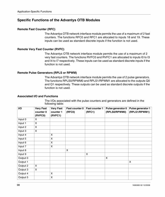
Application-Specific Functions
Specific Functions of the Advantys OTB Modules
Remote Fast Counter (RFC)
The Advantys OTB network interface module permits the use of a maximum of 2 fast counters. The functions RFC0 and RFC1 are allocated to inputs 18 and 19. These inputs can be used as standard discrete inputs if the function is not used.
Remote Very Fast Counter (RVFC)
The Advantys OTB network interface module permits the use of a maximum of 2 very fast counters. The functions RVFC0 and RVFC1 are allocated to inputs I0 to I3 and I4 to I7 respectively. These inputs can be used as standard discrete inputs if the function is not used.
Remote Pulse Generators (RPLS or RPWM)
The Advantys OTB network interface module permits the use of 2 pulse generators. The functions RPLS0/RPWM0 and RPLS1/RPWM1 are allocated to the outputs Q0 and Q1 respectively. These outputs can be used as standard discrete outputs if the function is not used.
Associated I/O and Functions
The I/Os associated with the pulse counters and generators are defined in the following table:
I/O Very Fast counter 0 (RVFC0)
Very Fast counter 1 (RVFC1)
Fast counter 0 (RFC0)
Fast counter 1 (RFC1)
Pulse generator 0 (RPLS0/RPWM0)
Pulse generator 1 (RPLS1/RPWM1)
Input 0 X
Input 1 X
Input 2 X
Input 3 X
Input 4 X
Input 5 X
Input 6 X
Input 7 X
Input 8 X
Input 9 X
Output 0 X
Output 1 X
Output 2 X
Output 3 X
Output 4 X
Output 5 X
98 1606383 02 12/2008
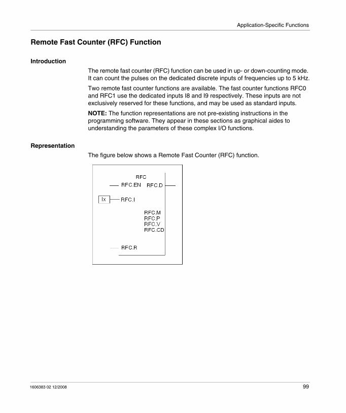
Application-Specific Functions
Remote Fast Counter (RFC) Function
Introduction
The remote fast counter (RFC) function can be used in up- or down-counting mode. It can count the pulses on the dedicated discrete inputs of frequencies up to 5 kHz.
Two remote fast counter functions are available. The fast counter functions RFC0 and RFC1 use the dedicated inputs I8 and I9 respectively. These inputs are not exclusively reserved for these functions, and may be used as standard inputs.
NOTE: The function representations are not pre-existing instructions in the programming software. They appear in these sections as graphical aides to understanding the parameters of these complex I/O functions.
Representation
The figure below shows a Remote Fast Counter (RFC) function.
1606383 02 12/2008 99
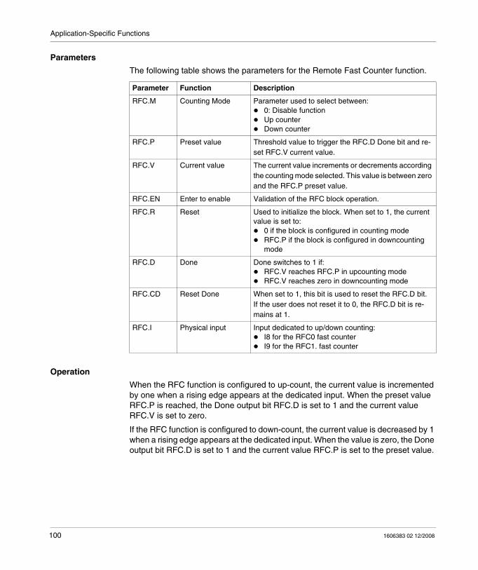
Application-Specific Functions
Parameters
The following table shows the parameters for the Remote Fast Counter function.
Operation
When the RFC function is configured to up-count, the current value is incremented by one when a rising edge appears at the dedicated input. When the preset value RFC.P is reached, the Done output bit RFC.D is set to 1 and the current value RFC.V is set to zero.
If the RFC function is configured to down-count, the current value is decreased by 1 when a rising edge appears at the dedicated input. When the value is zero, the Done output bit RFC.D is set to 1 and the current value RFC.P is set to the preset value.
Parameter Function Description
RFC.M Counting Mode Parameter used to select between:0: Disable functionUp counterDown counter
RFC.P Preset value Threshold value to trigger the RFC.D Done bit and re-set RFC.V current value.
RFC.V Current value The current value increments or decrements according the counting mode selected. This value is between zero and the RFC.P preset value.
RFC.EN Enter to enable Validation of the RFC block operation.
RFC.R Reset Used to initialize the block. When set to 1, the current value is set to:
0 if the block is configured in counting modeRFC.P if the block is configured in downcounting mode
RFC.D Done Done switches to 1 if:RFC.V reaches RFC.P in upcounting modeRFC.V reaches zero in downcounting mode
RFC.CD Reset Done When set to 1, this bit is used to reset the RFC.D bit.If the user does not reset it to 0, the RFC.D bit is re-mains at 1.
RFC.I Physical input Input dedicated to up/down counting:I8 for the RFC0 fast counterI9 for the RFC1. fast counter
100 1606383 02 12/2008
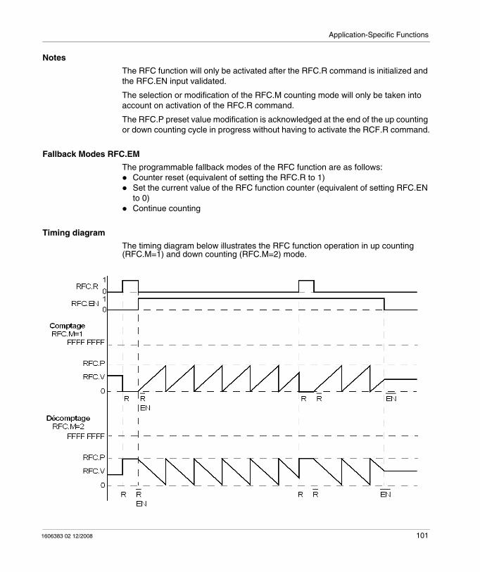
Application-Specific Functions
Notes
The RFC function will only be activated after the RFC.R command is initialized and the RFC.EN input validated.
The selection or modification of the RFC.M counting mode will only be taken into account on activation of the RFC.R command.
The RFC.P preset value modification is acknowledged at the end of the up counting or down counting cycle in progress without having to activate the RCF.R command.
Fallback Modes RFC.EM
The programmable fallback modes of the RFC function are as follows:Counter reset (equivalent of setting the RFC.R to 1)Set the current value of the RFC function counter (equivalent of setting RFC.EN to 0)Continue counting
Timing diagram
The timing diagram below illustrates the RFC function operation in up counting (RFC.M=1) and down counting (RFC.M=2) mode.
1606383 02 12/2008 101
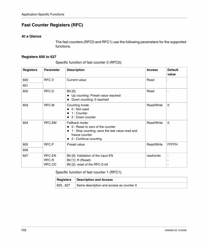
Application-Specific Functions
Fast Counter Registers (RFC)
At a Glance
The fast counters (RFC0 and RFC1) use the following parameters for the supported functions.
Registers 600 to 627
Specific function of fast counter 0 (RFC0).
Specific function of fast counter 1 (RFC1).
Registers Parameter Description Access Default value
600 RFC.V Current value Read -
601
602 RFC.D Bit [0]: Up counting: Preset value reachedDown counting: 0 reached
Read -
603 RFC.M Counting mode:0 : Not used1 : Counter2 : Down counter
Read/Write 0
604 RFC.EM Fallback mode:0 : Reset to zero of the counter1 : Stop counting, save the last value read and freeze counter 2 : Continue counting
Read/Write 0
605 RFC.P Preset value Read/Write FFFFH
606
607 RFC.ENRFC.RRFC.CD
Bit [0]: Validation of the input ENBit [1]: R (Reset)Bit [2]: reset of the RFC.D bit
read/write ---
Registers Description and Access
620...627 Same description and access as counter 0
102 1606383 02 12/2008

Application-Specific Functions
Remote Very Fast Counter (RVFC) function
Introduction
The Remote Very Fast Counter (RVFC) function can be configured to perform any of the following functions:
Up/down counter2-phase up/down counterSingle up counterSingle down counterFrequency meter
Two very fast counters are available. The RVFC function supports counting of dedicated discrete inputs from 0 to 20 kHz. Very fast counters RVFC0 and RVFC1 each use the I/O dedicated to these functions.
A Remote Very Fast Counter (RVFC) has a value range between 0 and 4,294,967,295.
Notes
The RVFC function will only be activated after the RVFC.R parameter is initialized and the RVFC.EN input enabled.
Selection or modification of the RVFC.M counting mode will only be taken into account on activation of the RVFC.R command.
Dedicated I/O Assignments
The Remote Very Fast Counter (RVFC) functions use dedicated inputs and outputs. These inputs and outputs are not exclusively reserved for these functions, and can be used as normal discrete I/O.
1606383 02 12/2008 103
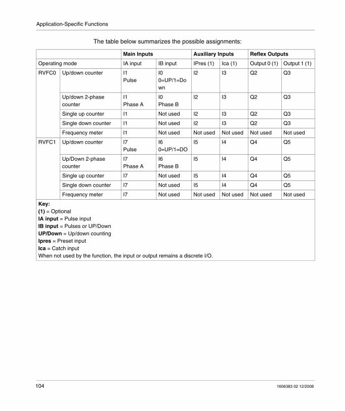
Application-Specific Functions
The table below summarizes the possible assignments:
Main Inputs Auxiliary Inputs Reflex Outputs
Operating mode IA input IB input IPres (1) Ica (1) Output 0 (1) Output 1 (1)
RVFC0 Up/down counter I1Pulse
I00=UP/1=Down
I2 I3 Q2 Q3
Up/down 2-phase counter
I1Phase A
I0Phase B
I2 I3 Q2 Q3
Single up counter I1 Not used I2 I3 Q2 Q3
Single down counter I1 Not used I2 I3 Q2 Q3
Frequency meter I1 Not used Not used Not used Not used Not used
RVFC1 Up/down counter I7Pulse
I60=UP/1=DO
I5 I4 Q4 Q5
Up/Down 2-phase counter
I7Phase A
I6Phase B
I5 I4 Q4 Q5
Single up counter I7 Not used I5 I4 Q4 Q5
Single down counter I7 Not used I5 I4 Q4 Q5
Frequency meter I7 Not used Not used Not used Not used Not used
Key:(1) = OptionalIA input = Pulse inputIB input = Pulses or UP/DownUP/Down = Up/down countingIpres = Preset inputIca = Catch inputWhen not used by the function, the input or output remains a discrete I/O.
104 1606383 02 12/2008
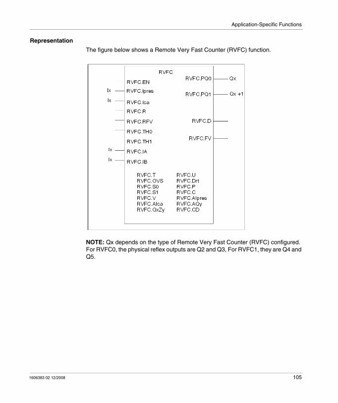
Application-Specific Functions
Representation
The figure below shows a Remote Very Fast Counter (RVFC) function.
NOTE: Qx depends on the type of Remote Very Fast Counter (RVFC) configured. For RVFC0, the physical reflex outputs are Q2 and Q3, For RVFC1, they are Q4 and Q5.
1606383 02 12/2008 105
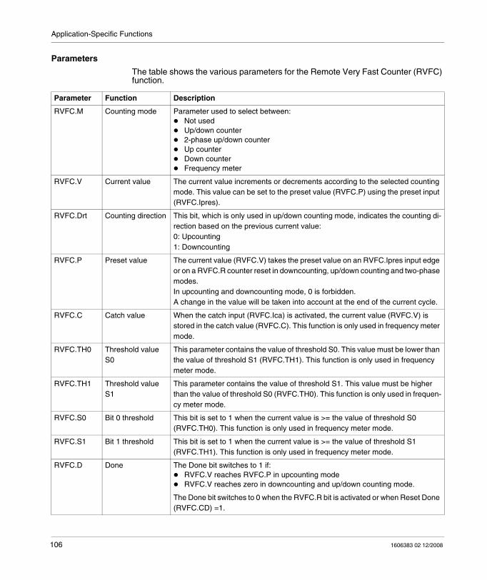
Application-Specific Functions
Parameters
The table shows the various parameters for the Remote Very Fast Counter (RVFC) function.
Parameter Function Description
RVFC.M Counting mode Parameter used to select between:Not usedUp/down counter2-phase up/down counterUp counterDown counterFrequency meter
RVFC.V Current value The current value increments or decrements according to the selected counting mode. This value can be set to the preset value (RVFC.P) using the preset input (RVFC.Ipres).
RVFC.Drt Counting direction This bit, which is only used in up/down counting mode, indicates the counting di-rection based on the previous current value:0: Upcounting1: Downcounting
RVFC.P Preset value The current value (RVFC.V) takes the preset value on an RVFC.Ipres input edge or on a RVFC.R counter reset in downcounting, up/down counting and two-phase modes.In upcounting and downcounting mode, 0 is forbidden.A change in the value will be taken into account at the end of the current cycle.
RVFC.C Catch value When the catch input (RVFC.Ica) is activated, the current value (RVFC.V) is stored in the catch value (RVFC.C). This function is only used in frequency meter mode.
RVFC.TH0 Threshold value S0
This parameter contains the value of threshold S0. This value must be lower than the value of threshold S1 (RVFC.TH1). This function is only used in frequency meter mode.
RVFC.TH1 Threshold value S1
This parameter contains the value of threshold S1. This value must be higher than the value of threshold S0 (RVFC.TH0). This function is only used in frequen-cy meter mode.
RVFC.S0 Bit 0 threshold This bit is set to 1 when the current value is >= the value of threshold S0 (RVFC.TH0). This function is only used in frequency meter mode.
RVFC.S1 Bit 1 threshold This bit is set to 1 when the current value is >= the value of threshold S1 (RVFC.TH1). This function is only used in frequency meter mode.
RVFC.D Done The Done bit switches to 1 if:RVFC.V reaches RVFC.P in upcounting modeRVFC.V reaches zero in downcounting and up/down counting mode.
The Done bit switches to 0 when the RVFC.R bit is activated or when Reset Done (RVFC.CD) =1.
106 1606383 02 12/2008
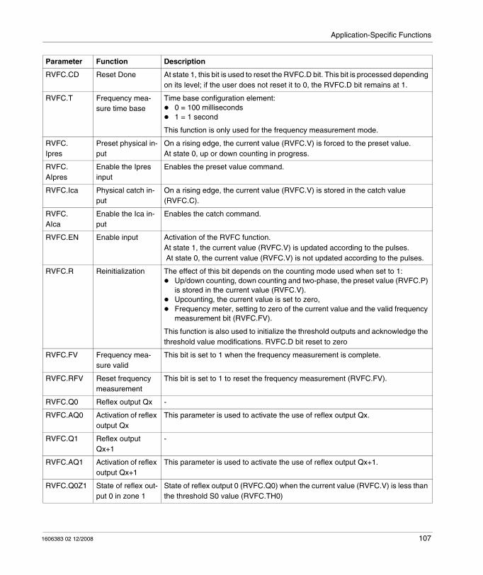
Application-Specific Functions
RVFC.CD Reset Done At state 1, this bit is used to reset the RVFC.D bit. This bit is processed depending on its level; if the user does not reset it to 0, the RVFC.D bit remains at 1.
RVFC.T Frequency mea-sure time base
Time base configuration element:0 = 100 milliseconds1 = 1 second
This function is only used for the frequency measurement mode.
RVFC.Ipres
Preset physical in-put
On a rising edge, the current value (RVFC.V) is forced to the preset value.At state 0, up or down counting in progress.
RVFC.AIpres
Enable the Ipres input
Enables the preset value command.
RVFC.Ica Physical catch in-put
On a rising edge, the current value (RVFC.V) is stored in the catch value (RVFC.C).
RVFC.AIca
Enable the Ica in-put
Enables the catch command.
RVFC.EN Enable input Activation of the RVFC function.At state 1, the current value (RVFC.V) is updated according to the pulses. At state 0, the current value (RVFC.V) is not updated according to the pulses.
RVFC.R Reinitialization The effect of this bit depends on the counting mode used when set to 1:Up/down counting, down counting and two-phase, the preset value (RVFC.P) is stored in the current value (RVFC.V).Upcounting, the current value is set to zero,Frequency meter, setting to zero of the current value and the valid frequency measurement bit (RVFC.FV).
This function is also used to initialize the threshold outputs and acknowledge the threshold value modifications. RVFC.D bit reset to zero
RVFC.FV Frequency mea-sure valid
This bit is set to 1 when the frequency measurement is complete.
RVFC.RFV Reset frequency measurement
This bit is set to 1 to reset the frequency measurement (RVFC.FV).
RVFC.Q0 Reflex output Qx -
RVFC.AQ0 Activation of reflex output Qx
This parameter is used to activate the use of reflex output Qx.
RVFC.Q1 Reflex output Qx+1
-
RVFC.AQ1 Activation of reflex output Qx+1
This parameter is used to activate the use of reflex output Qx+1.
RVFC.Q0Z1 State of reflex out-put 0 in zone 1
State of reflex output 0 (RVFC.Q0) when the current value (RVFC.V) is less than the threshold S0 value (RVFC.TH0)
Parameter Function Description
1606383 02 12/2008 107
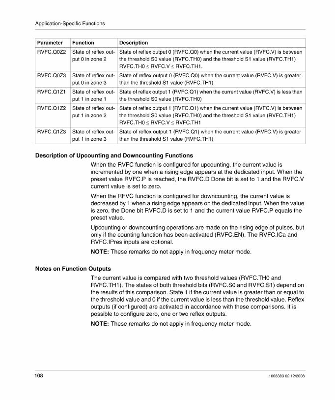
Application-Specific Functions
Description of Upcounting and Downcounting Functions
When the RVFC function is configured for upcounting, the current value is incremented by one when a rising edge appears at the dedicated input. When the preset value RVFC.P is reached, the RVFC.D Done bit is set to 1 and the RVFC.V current value is set to zero.
When the RFVC function is configured for downcounting, the current value is decreased by 1 when a rising edge appears on the dedicated input. When the value is zero, the Done bit RVFC.D is set to 1 and the current value RVFC.P equals the preset value.
Upcounting or downcounting operations are made on the rising edge of pulses, but only if the counting function has been activated (RVFC.EN). The RVFC.ICa and RVFC.IPres inputs are optional.
NOTE: These remarks do not apply in frequency meter mode.
Notes on Function Outputs
The current value is compared with two threshold values (RVFC.TH0 and RVFC.TH1). The states of both threshold bits (RVFC.S0 and RVFC.S1) depend on the results of this comparison. State 1 if the current value is greater than or equal to the threshold value and 0 if the current value is less than the threshold value. Reflex outputs (if configured) are activated in accordance with these comparisons. It is possible to configure zero, one or two reflex outputs.
NOTE: These remarks do not apply in frequency meter mode.
RVFC.Q0Z2 State of reflex out-put 0 in zone 2
State of reflex output 0 (RVFC.Q0) when the current value (RVFC.V) is between the threshold S0 value (RVFC.TH0) and the threshold S1 value (RVFC.TH1)RVFC.TH0 ≤ RVFC.V ≤ RVFC.TH1.
RVFC.Q0Z3 State of reflex out-put 0 in zone 3
State of reflex output 0 (RVFC.Q0) when the current value (RVFC.V) is greater than the threshold S1 value (RVFC.TH1)
RVFC.Q1Z1 State of reflex out-put 1 in zone 1
State of reflex output 1 (RVFC.Q1) when the current value (RVFC.V) is less than the threshold S0 value (RVFC.TH0)
RVFC.Q1Z2 State of reflex out-put 1 in zone 2
State of reflex output 1 (RVFC.Q1) when the current value (RVFC.V) is between the threshold S0 value (RVFC.TH0) and the threshold S1 value (RVFC.TH1)RVFC.TH0 ≤ RVFC.V ≤ RVFC.TH1
RVFC.Q1Z3 State of reflex out-put 1 in zone 3
State of reflex output 1 (RVFC.Q1) when the current value (RVFC.V) is greater than the threshold S1 value (RVFC.TH1)
Parameter Function Description
108 1606383 02 12/2008
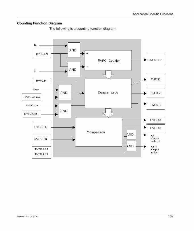
Application-Specific Functions
Counting Function Diagram
The following is a counting function diagram:
1606383 02 12/2008 109
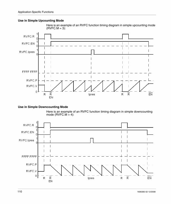
Application-Specific Functions
Use in Simple Upcounting Mode
Here is an example of an RVFC function timing diagram in simple upcounting mode (RVFC.M = 3):
Use in Simple Downcounting Mode
Here is an example of an RVFC function timing diagram in simple downcounting mode (RVFC.M = 4):
110 1606383 02 12/2008
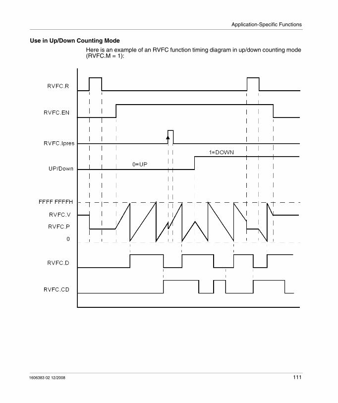
Application-Specific Functions
Use in Up/Down Counting Mode
Here is an example of an RVFC function timing diagram in up/down counting mode (RVFC.M = 1):
1606383 02 12/2008 111
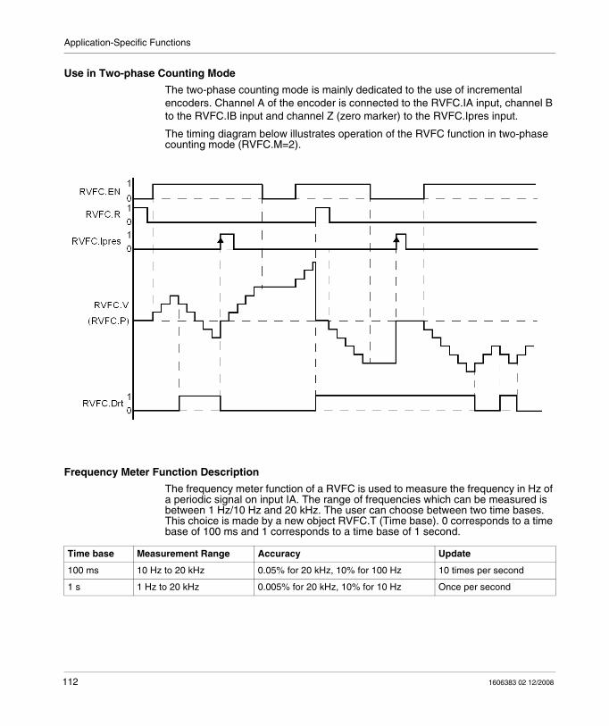
Application-Specific Functions
Use in Two-phase Counting Mode
The two-phase counting mode is mainly dedicated to the use of incremental encoders. Channel A of the encoder is connected to the RVFC.IA input, channel B to the RVFC.IB input and channel Z (zero marker) to the RVFC.Ipres input.
The timing diagram below illustrates operation of the RVFC function in two-phase counting mode (RVFC.M=2).
Frequency Meter Function Description
The frequency meter function of a RVFC is used to measure the frequency in Hz of a periodic signal on input IA. The range of frequencies which can be measured is between 1 Hz/10 Hz and 20 kHz. The user can choose between two time bases. This choice is made by a new object RVFC.T (Time base). 0 corresponds to a time base of 100 ms and 1 corresponds to a time base of 1 second.
Time base Measurement Range Accuracy Update
100 ms 10 Hz to 20 kHz 0.05% for 20 kHz, 10% for 100 Hz 10 times per second
1 s 1 Hz to 20 kHz 0.005% for 20 kHz, 10% for 10 Hz Once per second
112 1606383 02 12/2008
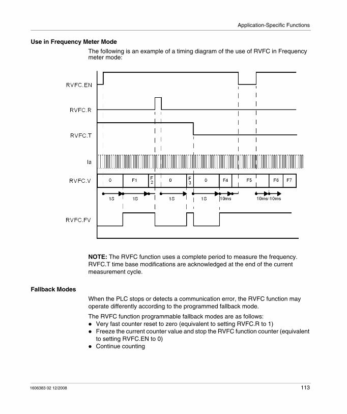
Application-Specific Functions
Use in Frequency Meter Mode
The following is an example of a timing diagram of the use of RVFC in Frequency meter mode:
NOTE: The RVFC function uses a complete period to measure the frequency. RVFC.T time base modifications are acknowledged at the end of the current measurement cycle.
Fallback Modes
When the PLC stops or detects a communication error, the RVFC function may operate differently according to the programmed fallback mode.
The RVFC function programmable fallback modes are as follows:Very fast counter reset to zero (equivalent to setting RVFC.R to 1)Freeze the current counter value and stop the RVFC function counter (equivalent to setting RVFC.EN to 0)Continue counting
1606383 02 12/2008 113

Application-Specific Functions
Remote Very Fast Counter Registers (RVFC)
At a Glance
The very fast counters (RVFC0 and RVFC1) use the following parameters for the supported functions.
Registers 700 to 734
Specific function of Remote Very Fast Counter 0 (RVFC0):
Registers Parameter Description Access Default value
700 RVFC.V Current value Read -
701 -
702 RVFC.Drt Bit[0]: Count direction Read -
RVFC.D Bit [1]: Output overshoot -
RVFC.S0 Bit [2]: Threshold S0 reached. When set to 1, the current value is greater than S0.
-
RVFC.S1 Bit [3]: Threshold S1 reached. When set to 1, the current value is greater than S1.
-
RVFC.FV Bit [4]: Measurement frequency valid -
703 RVFC.C Catch value Read -
704 -
705 RVFC.M Counting mode:0 : Not used1 : Up/Down counter2 : 2-phase counter3 : Single up counter4 : Single down counter5 : Frequency meter
Read/Write 0
706 RVFC.P Preset value Read/Write FFFFH
707 FFFFH
114 1606383 02 12/2008
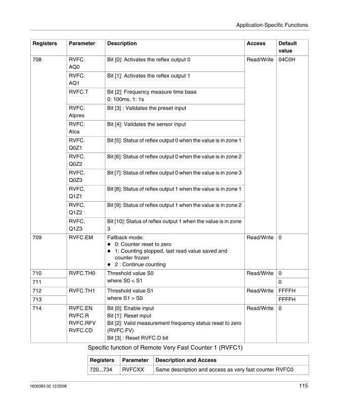
Application-Specific Functions
Specific function of Remote Very Fast Counter 1 (RVFC1)
708 RVFC.AQ0
Bit [0]: Activates the reflex output 0 Read/Write 04C0H
RVFC.AQ1
Bit [1]: Activates the reflex output 1
RVFC.T Bit [2]: Frequency measure time base0: 100ms, 1: 1s
RVFC.AIpres
Bit [3] : Validates the preset input
RVFC.AIca
Bit [4]: Validates the sensor input
RVFC.Q0Z1
Bit [5]: Status of reflex output 0 when the value is in zone 1
RVFC.Q0Z2
Bit [6]: Status of reflex output 0 when the value is in zone 2
RVFC.Q0Z3
Bit [7]: Status of reflex output 0 when the value is in zone 3
RVFC.Q1Z1
Bit [8]: Status of reflex output 1 when the value is in zone 1
RVFC.Q1Z2
Bit [9]: Status of reflex output 1 when the value is in zone 2
RVFC.Q1Z3
Bit [10]: Status of reflex output 1 when the value is in zone 3
709 RVFC.EM Fallback mode:0: Counter reset to zero1: Counting stopped, last read value saved and counter frozen2 : Continue counting
Read/Write 0
710 RVFC.TH0 Threshold value S0where S0 < S1
Read/Write 0
711 0
712 RVFC.TH1 Threshold value S1where S1 > S0
Read/Write FFFFH
713 FFFFH
714 RVFC.ENRVFC.RRVFC.RFVRVFC.CD
Bit [0]: Enable inputBit [1]: Reset inputBit [2]: Valid measurement frequency status reset to zero (RVFC.FV)Bit [3] : Reset RVFC.D bit
Read/Write 0
Registers Parameter Description Access Default value
Registers Parameter Description and Access
720...734 RVFCXX Same description and access as very fast counter RVFC0
1606383 02 12/2008 115
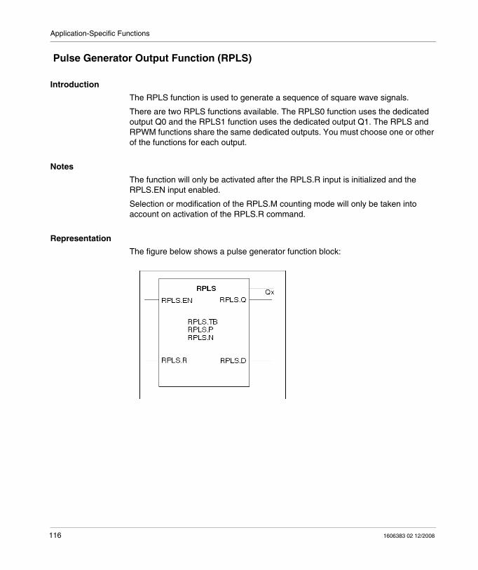
Application-Specific Functions
Pulse Generator Output Function (RPLS)
Introduction
The RPLS function is used to generate a sequence of square wave signals.
There are two RPLS functions available. The RPLS0 function uses the dedicated output Q0 and the RPLS1 function uses the dedicated output Q1. The RPLS and RPWM functions share the same dedicated outputs. You must choose one or other of the functions for each output.
Notes
The function will only be activated after the RPLS.R input is initialized and the RPLS.EN input enabled.
Selection or modification of the RPLS.M counting mode will only be taken into account on activation of the RPLS.R command.
Representation
The figure below shows a pulse generator function block:
116 1606383 02 12/2008
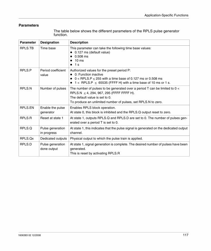
Application-Specific Functions
Parameters
The table below shows the different parameters of the RPLS pulse generator function.
Parameter Designation Description
RPLS.TB Time base This parameter can take the following time base values: 0.127 ms (default value)0.508 ms10 ms1 s
RPLS.P Period coefficient value
Authorized values for the preset period P: 0: Function inactive0 < RPLS.P < 255 with a time base of 0.127 ms or 0.508 ms1 < RPLS.P < 65535 (FFFF H) with a time base of 10 ms or 1 s.
RPLS.N Number of pulses The number of pulses to be generated over a period T can be limited to 0 < RPLS.N < 4, 294, 967, 295 (FFFF FFFF H).The default value is set to 0.To produce an unlimited number of pulses, set RPLS.N to zero.
RPLS.EN Enable the pulse generator
Enables RPLS block operation.At state 0, this block is inhibited and the RPLS.Q output reset to zero.
RPLS.R Reset at state 1 At state 1, outputs RPLS.Q and RPLS.D are set to 0. The number of pulses gen-erated over a period T is set to 0.
RPLS.Q Pulse generation in progress
At state 1, this indicates that the pulse signal is generated on the dedicated output channel.
RPLS.Qx Dedicated outputs Physical output to which the pulse train is applied.
RPLS.D Pulse generation done output
At state 1, signal generation is complete. The desired number of pulses have been generated.This is reset by activating RPLS.R
1606383 02 12/2008 117
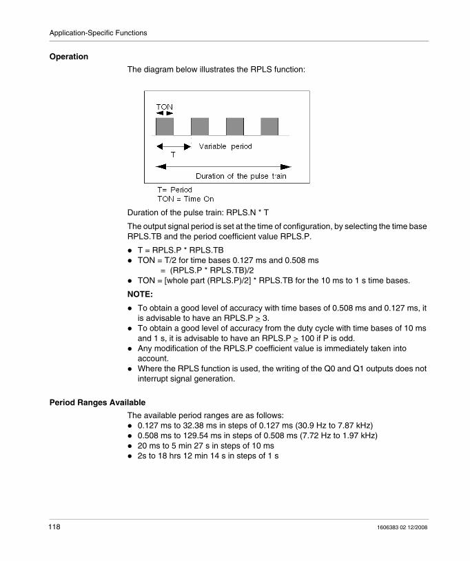
Application-Specific Functions
Operation
The diagram below illustrates the RPLS function:
Duration of the pulse train: RPLS.N * T
The output signal period is set at the time of configuration, by selecting the time base RPLS.TB and the period coefficient value RPLS.P.
T = RPLS.P * RPLS.TBTON = T/2 for time bases 0.127 ms and 0.508 ms = (RPLS.P * RPLS.TB)/2TON = [whole part (RPLS.P)/2] * RPLS.TB for the 10 ms to 1 s time bases.
NOTE:
To obtain a good level of accuracy with time bases of 0.508 ms and 0.127 ms, it is advisable to have an RPLS.P > 3. To obtain a good level of accuracy from the duty cycle with time bases of 10 ms and 1 s, it is advisable to have an RPLS.P > 100 if P is odd.Any modification of the RPLS.P coefficient value is immediately taken into account.Where the RPLS function is used, the writing of the Q0 and Q1 outputs does not interrupt signal generation.
Period Ranges Available
The available period ranges are as follows:0.127 ms to 32.38 ms in steps of 0.127 ms (30.9 Hz to 7.87 kHz)0.508 ms to 129.54 ms in steps of 0.508 ms (7.72 Hz to 1.97 kHz)20 ms to 5 min 27 s in steps of 10 ms2s to 18 hrs 12 min 14 s in steps of 1 s
118 1606383 02 12/2008
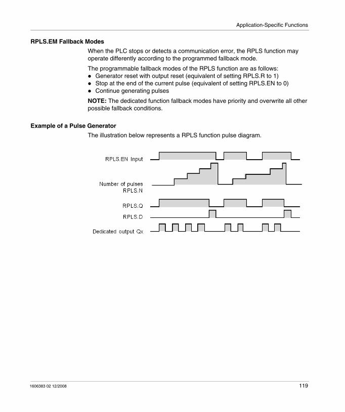
Application-Specific Functions
RPLS.EM Fallback Modes
When the PLC stops or detects a communication error, the RPLS function may operate differently according to the programmed fallback mode.
The programmable fallback modes of the RPLS function are as follows:Generator reset with output reset (equivalent of setting RPLS.R to 1)Stop at the end of the current pulse (equivalent of setting RPLS.EN to 0)Continue generating pulses
NOTE: The dedicated function fallback modes have priority and overwrite all other possible fallback conditions.
Example of a Pulse Generator
The illustration below represents a RPLS function pulse diagram.
1606383 02 12/2008 119
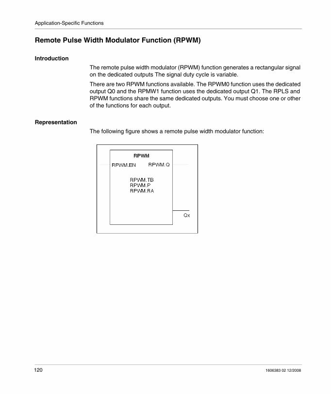
Application-Specific Functions
Remote Pulse Width Modulator Function (RPWM)
Introduction
The remote pulse width modulator (RPWM) function generates a rectangular signal on the dedicated outputs The signal duty cycle is variable.
There are two RPWM functions available. The RPWM0 function uses the dedicated output Q0 and the RPMW1 function uses the dedicated output Q1. The RPLS and RPWM functions share the same dedicated outputs. You must choose one or other of the functions for each output.
Representation
The following figure shows a remote pulse width modulator function:
120 1606383 02 12/2008
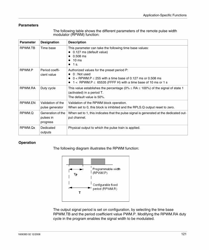
Application-Specific Functions
Parameters
The following table shows the different parameters of the remote pulse width modulator (RPWM) function:
Operation
The following diagram illustrates the RPWM function:
The output signal period is set on configuration, by selecting the time base RPWM.TB and the period coefficient value PWM.P. Modifying the RPWM.RA duty cycle in the program enables the signal width to be modulated.
Parameter Designation Description
RPWM.TB Time base This parameter can take the following time base values: 0.127 ms (default value)0.508 ms10 ms1 s.
RPWM.P Period coeffi-cient value
Authorized values for the preset period P: 0 : Not used0 < RPWM.P ≤ 255 with a time base of 0.127 ms or 0.508 ms1 < RPWM.P ≤ 65535 (FFFF H) with a time base of 10 ms or 1 s
RPWM.RA Duty cycle This value establishes the percentage (0% ≤ RA ≤ 100%) of the signal of state 1 (activated) in a period T.The default value is 50%.
RPWM.EN Validation of the pulse generator
Validation of the RPWM block operation.When set to 0, this block is inhibited and the RPLS.Q output reset to zero.
RPWM.Q Generation of the pulses in progress
When set to 1, this indicates that the pulse signal is generated at the dedicated out-put channel.
RPWM.Qx Dedicated outputs
Physical output to which the pulse train is applied.
1606383 02 12/2008 121

Application-Specific Functions
Range of Periods
The coefficient value and the time base can be modified during configuration. They are used to set the signal period T = RPWM.P * TB. The range of periods available:
0.127 ms to 32.38 ms in steps of 0.127 ms (30.9 Hz to 7.87 kHz)0.508 ms to 129.54 ms in steps of 0.508 ms (7.72 Hz to 1.97 kHz)10 ms to 5 min 27 s in steps of 10 ms2s at 18hrs 12min 14s in steps of 1 s
Pulse Modulation
Calculation of the Tp width: Tp = T * (RPWM.RA/100)
If the signal period is programmed to 500 ms, then Where the RPWM.RA ratio is set to 20%, the duration of the signal at state 1 is then: 20 % x 500 ms = 100 msWhere the RPWM.RA ratio is set to 50 % (duration = 250 ms)Where the RPWM.RA ratio is set to 80 % (duration = 400 ms)
Fallback Modes RPWM.EM
When the PLC stops or detects a communication error, the RPWM function may operate differently according to the programmed fallback mode.
The programmable fallback modes of the RPWM function are as follows:Generator reset with output resetStop at the end of the current interval (equivalent of setting RPWM.EN to 0)Continue generating pulses
Example of a Pulse Generator with Pulse Width Modulation
Below is an illustration of a pulse diagram for the RPWM function with varying duty cycles.
122 1606383 02 12/2008
Application-Specific Functions
Remote Pulse Generators (RPLS, RPWM) Registers
At a Glance
The pulse generators (RPLS) and pulse width modulation generators (RPWM) use the following parameters for the supported functions.
Registers 800 to 828
Remote pulse generator specific function (RPLS0 or RPWM0).
Registers Parameter Description Access Default value
800 RPLS.QRPWM.Q
Bit [0]: Q output. At state 1, it indicates that the pulse signal is generated at the dedicated output configured.
Read -
RPLS.DRPWM.D
Bit [1]: Output D. When set to 1, signal generation is com-plete. The number of desired pulses has been reached.
-
801 RPLS.M/RPWM.M
Operating mode:0: Not used1: PLS2: PWM
read/write 0
802 RPLS.TBRPWM.TB
Time base:0: 0.127 ms1: 0.508 ms2: 10 ms3: 1 s
Read/Write 0
803 RPLS.PRPWM.P
Preset period: P0: Not used0< P < 255 with a time base of 0.127 ms or 0.508 ms1< P < 65535 (FFFFH) with a time base of 10 ms or 1 s
Read/Write 1
804805
RPLS.N Number of pulses:0: Unlimited number of pulses1< N < 4 294 967 295 (FFFF FFFFH)
read/write 00
806 RPWM.RA Duty cycle: 0% ≤ R ≤ 100%.Duration of high status / Period
Read/Write 32H (50%)
807 RPLS.EMRPWM.EM
Fallback mode:0: Generator reset with zeroing of output1: Stop at the end of current interval2: continue generating pulses
read/write 0
808 RPLS. ENRPWM.EN
Bit [0]: Pulse generation input. When set to 1, the pulse gen-eration is produced on the dedicated output. When set to 0, the output is set to 0.
Read/Write 0
RPLS. RRPWM.R
Bit [1]: Generator reset input. When set to 1, outputs Q and D are reset to 0. The number of pulses generated over a pe-riod T is reset to 0.
1606383 02 12/2008 123

Application-Specific Functions
Specific function of RPLS1 or RPWM1.
Registers Description and Access
820...828 Description and access identical to those of the RPLS0 or RPWM0 functions
124 1606383 02 12/2008
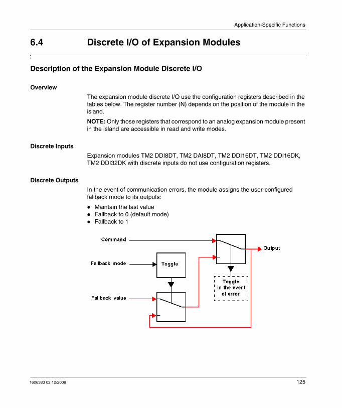
Application-Specific Functions
6.4 Discrete I/O of Expansion Modules
Description of the Expansion Module Discrete I/O
Overview
The expansion module discrete I/O use the configuration registers described in the tables below. The register number (N) depends on the position of the module in the island.
NOTE: Only those registers that correspond to an analog expansion module present in the island are accessible in read and write modes.
Discrete Inputs
Expansion modules TM2 DDI8DT, TM2 DAI8DT, TM2 DDI16DT, TM2 DDI16DK, TM2 DDI32DK with discrete inputs do not use configuration registers.
Discrete Outputs
In the event of communication errors, the module assigns the user-configured fallback mode to its outputs:
Maintain the last valueFallback to 0 (default mode)Fallback to 1
1606383 02 12/2008 125
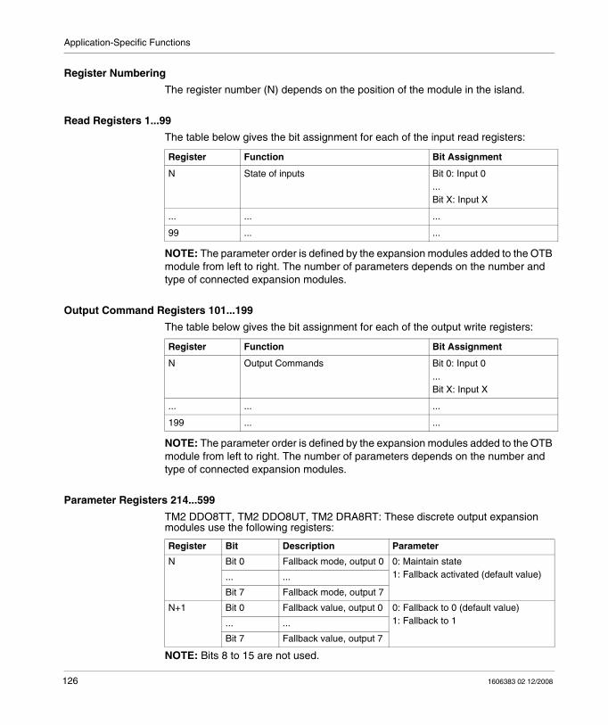
Application-Specific Functions
Register Numbering
The register number (N) depends on the position of the module in the island.
Read Registers 1...99
The table below gives the bit assignment for each of the input read registers:
NOTE: The parameter order is defined by the expansion modules added to the OTB module from left to right. The number of parameters depends on the number and type of connected expansion modules.
Output Command Registers 101...199
The table below gives the bit assignment for each of the output write registers:
NOTE: The parameter order is defined by the expansion modules added to the OTB module from left to right. The number of parameters depends on the number and type of connected expansion modules.
Parameter Registers 214...599
TM2 DDO8TT, TM2 DDO8UT, TM2 DRA8RT: These discrete output expansion modules use the following registers:
NOTE: Bits 8 to 15 are not used.
Register Function Bit Assignment
N State of inputs Bit 0: Input 0...Bit X: Input X
... ... ...
99 ... ...
Register Function Bit Assignment
N Output Commands Bit 0: Input 0...Bit X: Input X
... ... ...
199 ... ...
Register Bit Description Parameter
N Bit 0 Fallback mode, output 0 0: Maintain state1: Fallback activated (default value)... ...
Bit 7 Fallback mode, output 7
N+1 Bit 0 Fallback value, output 0 0: Fallback to 0 (default value)1: Fallback to 1... ...
Bit 7 Fallback value, output 7
126 1606383 02 12/2008
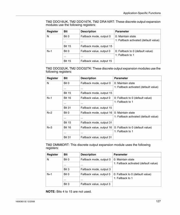
Application-Specific Functions
TM2 DDO16UK, TM2 DDO16TK, TM2 DRA16RT: These discrete output expansion modules use the following registers:
TM2 DDO32UK, TM2 DDO32TK: These discrete output expansion modules use the following registers:
TM2 DMM8DRT: This discrete output expansion module uses the following registers:
NOTE: Bits 4 to 15 are not used.
Register Bit Description Parameter
N Bit 0 Fallback mode, output 0 0: Maintain state1: Fallback activated (default value)... ...
Bit 15 Fallback mode, output 15
N+1 Bit 0 Fallback value, output 0 0: Fallback to 0 (default value)1: Fallback to 1... ...
Bit 15 Fallback value, output 15
Register Bit Description Parameter
N Bit 0 Fallback mode, output 0 0: Maintain state1: Fallback activated (default value)... ...
Bit 15 Fallback mode, output 15
N+1 Bit 16 Fallback value, output 0 0: Fallback to 0 (default value)1: Fallback to 1... ...
Bit 31 Fallback value, output 15
N+2 Bit 0 Fallback mode, output 16 0: Maintain state1: Fallback activated (default value)... ...
Bit 15 Fallback mode, output 31
N+3 Bit 16 Fallback value, output 16 0: Fallback to 0 (default value)1: Fallback to 1... ...
Bit 31 Fallback value, output 31
Register Bit Description Parameter
N Bit 0 Fallback mode, output 0 0: Maintain state1: Fallback activated (default value)... ...
Bit 3 Fallback mode, output 3
N+1 Bit 0 Fallback value, output 0 0: Fallback to 0 (default value)1: Fallback to 1... ...
Bit 3 Fallback value, output 3
1606383 02 12/2008 127

Application-Specific Functions
TM2 DMM24DRF: This discrete output expansion module uses the following registers:
NOTE: Bits 8 to 15 are not used.
Register Bit Description Parameter
N Bit 0 Fallback mode, output 0 0: Maintain state1: Fallback activated (default value)... ...
Bit 7 Fallback mode, output 7
N+1 Bit 0 Fallback value, output 0 0: Fallback to 0 (default value)1: Fallback to 1... ...
Bit 7 Fallback value, output 7
128 1606383 02 12/2008
Application-Specific Functions
6.5 Analog I/O of Expansion Modules
Introduction
This section shows how analog I/Os of expansion modules are used.
What's in this Section?
This section contains the following topics:
Topic Page
Description of the Expansion Module Analog I/O 130
TM2 AMI2HT Expansion Module Registers 133
TM2 AMO1HT Expansion Module Registers 134
TM2 AMM3HT Expansion Module Registers 135
TM2 AMM6HT Expansion Module Registers 137
TM2 ALM3LT Expansion Module Registers 139
TM2 AVO2HT Expansion Module Registers 141
TM2 AMI2LT Expansion Module Registers 142
TM2 AMI4LT Expansion Module Registers 143
TM2 AMI8HT Expansion Module Registers 144
TM2 ARI8HT Expansion Module Registers 146
TM2 ARI8LT and TM2 ARI8LRJ Expansion Module Registers 149
1606383 02 12/2008 129
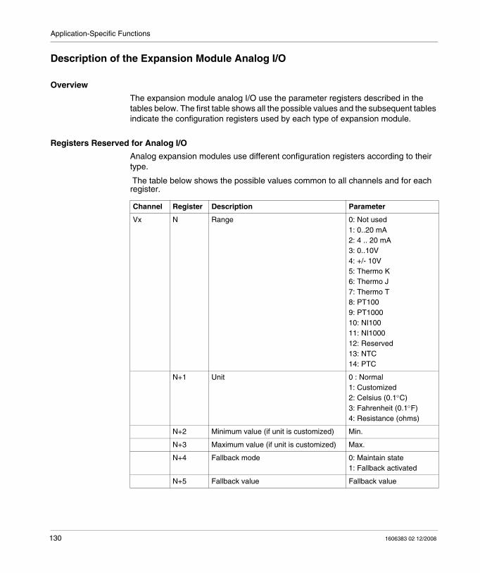
Application-Specific Functions
Description of the Expansion Module Analog I/O
Overview
The expansion module analog I/O use the parameter registers described in the tables below. The first table shows all the possible values and the subsequent tables indicate the configuration registers used by each type of expansion module.
Registers Reserved for Analog I/O
Analog expansion modules use different configuration registers according to their type.
The table below shows the possible values common to all channels and for each register.
Channel Register Description Parameter
Vx N Range 0: Not used1: 0..20 mA2: 4 .. 20 mA3: 0..10V 4: +/- 10V5: Thermo K6: Thermo J7: Thermo T8: PT1009: PT100010: NI10011: NI100012: Reserved13: NTC14: PTC
N+1 Unit 0 : Normal1: Customized2: Celsius (0.1°C)3: Fahrenheit (0.1°F)4: Resistance (ohms)
N+2 Minimum value (if unit is customized) Min.
N+3 Maximum value (if unit is customized) Max.
N+4 Fallback mode 0: Maintain state1: Fallback activated
N+5 Fallback value Fallback value
130 1606383 02 12/2008
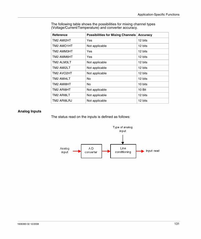
Application-Specific Functions
The following table shows the possibilities for mixing channel types (Voltage/Current/Temperature) and converter accuracy.
Analog Inputs
The status read on the inputs is defined as follows:
Reference Possibilities for Mixing Channels Accuracy
TM2 AMI2HT Yes 12 bits
TM2 AMO1HT Not applicable 12 bits
TM2 AMM3HT Yes 12 bits
TM2 AMM6HT Yes 12 bits
TM2 ALM3LT Not applicable 12 bits
TM2 AMI2LT Not applicable 12 bits
TM2 AVO2HT Not applicable 12 bits
TM2 AMI4LT No 12 bits
TM2 AMI8HT No 10 bits
TM2 ARI8HT Not applicable 10 Bit
TM2 ARI8LT Not applicable 12 bits
TM2 ARI8LRJ Not applicable 12 bits
1606383 02 12/2008 131
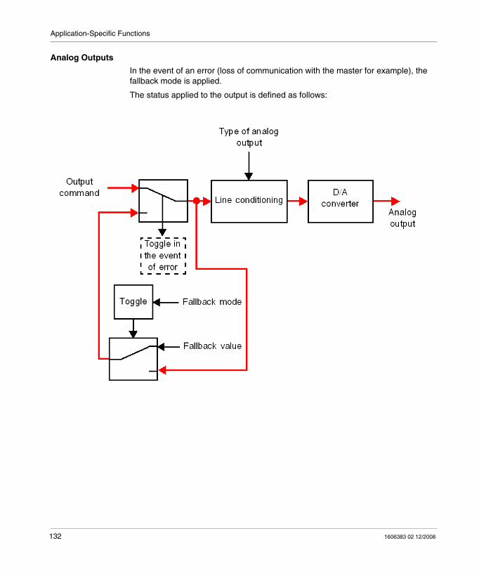
Application-Specific Functions
Analog Outputs
In the event of an error (loss of communication with the master for example), the fallback mode is applied.
The status applied to the output is defined as follows:
132 1606383 02 12/2008
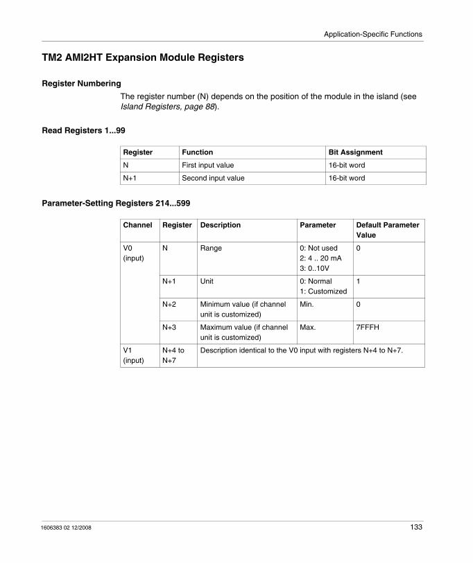
Application-Specific Functions
TM2 AMI2HT Expansion Module Registers
Register Numbering
The register number (N) depends on the position of the module in the island (see Island Registers, page 88).
Read Registers 1...99
Parameter-Setting Registers 214...599
Register Function Bit Assignment
N First input value 16-bit word
N+1 Second input value 16-bit word
Channel Register Description Parameter Default Parameter Value
V0(input)
N Range 0: Not used2: 4 .. 20 mA3: 0..10V
0
N+1 Unit 0: Normal1: Customized
1
N+2 Minimum value (if channel unit is customized)
Min. 0
N+3 Maximum value (if channel unit is customized)
Max. 7FFFH
V1(input)
N+4 to N+7
Description identical to the V0 input with registers N+4 to N+7.
1606383 02 12/2008 133
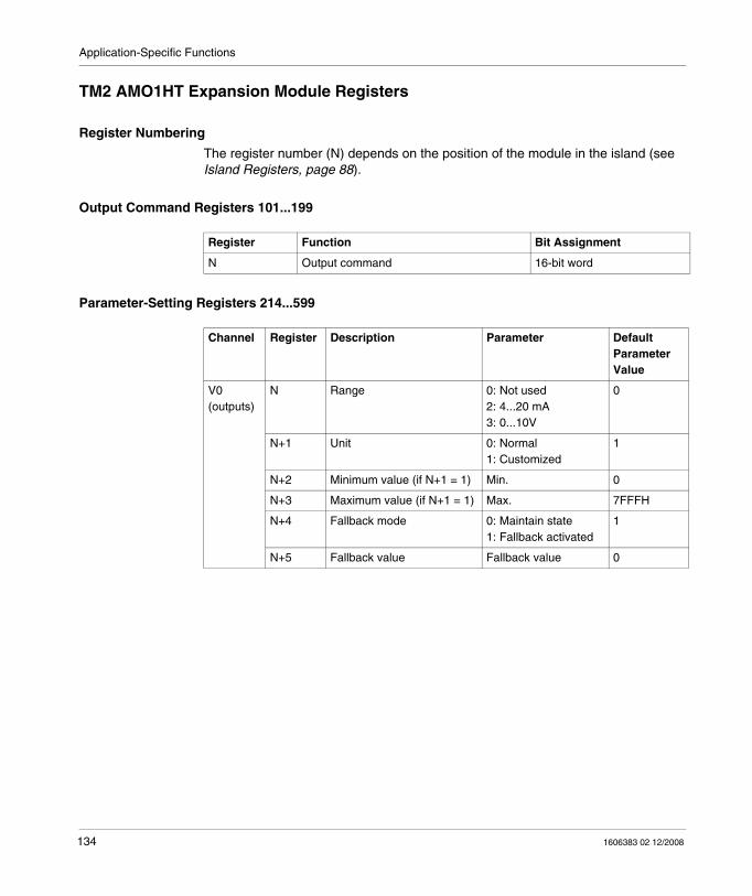
Application-Specific Functions
TM2 AMO1HT Expansion Module Registers
Register Numbering
The register number (N) depends on the position of the module in the island (see Island Registers, page 88).
Output Command Registers 101...199
Parameter-Setting Registers 214...599
Register Function Bit Assignment
N Output command 16-bit word
Channel Register Description Parameter Default Parameter Value
V0(outputs)
N Range 0: Not used2: 4...20 mA3: 0...10V
0
N+1 Unit 0: Normal1: Customized
1
N+2 Minimum value (if N+1 = 1) Min. 0
N+3 Maximum value (if N+1 = 1) Max. 7FFFH
N+4 Fallback mode 0: Maintain state1: Fallback activated
1
N+5 Fallback value Fallback value 0
134 1606383 02 12/2008
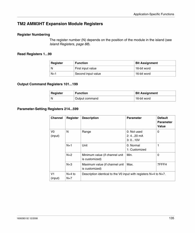
Application-Specific Functions
TM2 AMM3HT Expansion Module Registers
Register Numbering
The register number (N) depends on the position of the module in the island (see Island Registers, page 88).
Read Registers 1...99
Output Command Registers 101...199
Parameter-Setting Registers 214...599
Register Function Bit Assignment
N First input value 16-bit word
N+1 Second input value 16-bit word
Register Function Bit Assignment
N Output command 16-bit word
Channel Register Description Parameter Default Parameter Value
V0(input)
N Range 0: Not used2: 4...20 mA3: 0...10V
0
N+1 Unit 0: Normal1: Customized
1
N+2 Minimum value (if channel unit is customized)
Min. 0
N+3 Maximum value (if channel unit is customized)
Max. 7FFFH
V1(input)
N+4 to N+7
Description identical to the V0 input with registers N+4 to N+7.
1606383 02 12/2008 135

Application-Specific Functions
V2(output)
N+8 Range 0: Not used2: 4...20 mA3: 0...10V
0
N+9 Unit 0: Normal1: Customized
1
N+10 Minimum value (if channel unit is customized)
Min. 0
N+11 Maximum value (if channel unit is customized)
Max. 7FFFH
N+12 Fallback mode 0: Maintain state1: Fallback activated
1
N+13 Fallback value Fallback value 0
Channel Register Description Parameter Default Parameter Value
136 1606383 02 12/2008
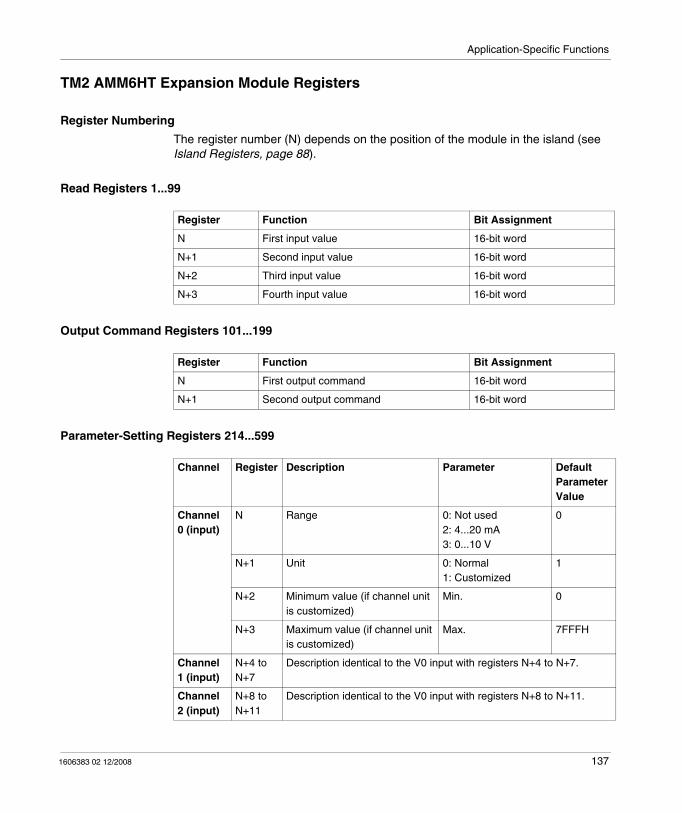
Application-Specific Functions
TM2 AMM6HT Expansion Module Registers
Register Numbering
The register number (N) depends on the position of the module in the island (see Island Registers, page 88).
Read Registers 1...99
Output Command Registers 101...199
Parameter-Setting Registers 214...599
Register Function Bit Assignment
N First input value 16-bit word
N+1 Second input value 16-bit word
N+2 Third input value 16-bit word
N+3 Fourth input value 16-bit word
Register Function Bit Assignment
N First output command 16-bit word
N+1 Second output command 16-bit word
Channel Register Description Parameter Default Parameter Value
Channel 0 (input)
N Range 0: Not used2: 4...20 mA3: 0...10 V
0
N+1 Unit 0: Normal1: Customized
1
N+2 Minimum value (if channel unit is customized)
Min. 0
N+3 Maximum value (if channel unit is customized)
Max. 7FFFH
Channel 1 (input)
N+4 to N+7
Description identical to the V0 input with registers N+4 to N+7.
Channel 2 (input)
N+8 to N+11
Description identical to the V0 input with registers N+8 to N+11.
1606383 02 12/2008 137
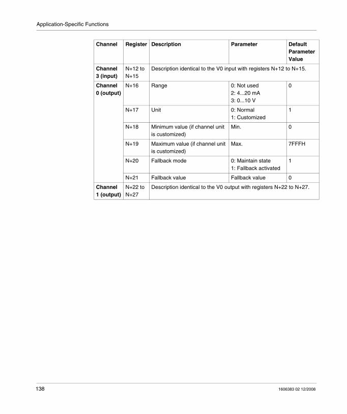
Application-Specific Functions
Channel 3 (input)
N+12 to N+15
Description identical to the V0 input with registers N+12 to N+15.
Channel 0 (output)
N+16 Range 0: Not used2: 4...20 mA3: 0...10 V
0
N+17 Unit 0: Normal1: Customized
1
N+18 Minimum value (if channel unit is customized)
Min. 0
N+19 Maximum value (if channel unit is customized)
Max. 7FFFH
N+20 Fallback mode 0: Maintain state1: Fallback activated
1
N+21 Fallback value Fallback value 0
Channel 1 (output)
N+22 to N+27
Description identical to the V0 output with registers N+22 to N+27.
Channel Register Description Parameter Default Parameter Value
138 1606383 02 12/2008
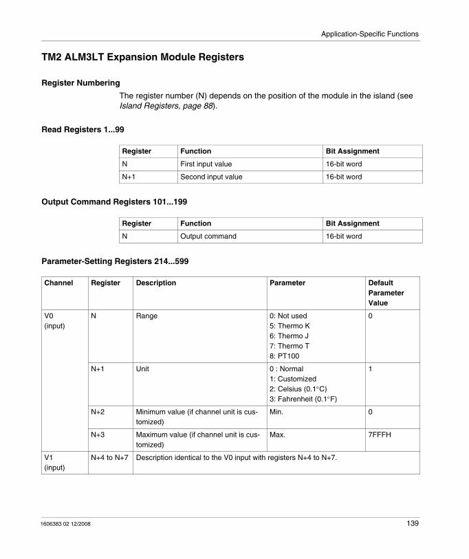
Application-Specific Functions
TM2 ALM3LT Expansion Module Registers
Register Numbering
The register number (N) depends on the position of the module in the island (see Island Registers, page 88).
Read Registers 1...99
Output Command Registers 101...199
Parameter-Setting Registers 214...599
Register Function Bit Assignment
N First input value 16-bit word
N+1 Second input value 16-bit word
Register Function Bit Assignment
N Output command 16-bit word
Channel Register Description Parameter Default Parameter Value
V0(input)
N Range 0: Not used5: Thermo K6: Thermo J7: Thermo T8: PT100
0
N+1 Unit 0 : Normal1: Customized2: Celsius (0.1°C)3: Fahrenheit (0.1°F)
1
N+2 Minimum value (if channel unit is cus-tomized)
Min. 0
N+3 Maximum value (if channel unit is cus-tomized)
Max. 7FFFH
V1(input)
N+4 to N+7 Description identical to the V0 input with registers N+4 to N+7.
1606383 02 12/2008 139
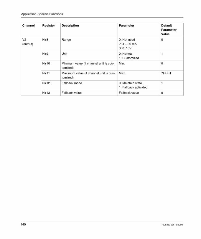
Application-Specific Functions
V2(output)
N+8 Range 0: Not used2: 4 .. 20 mA3: 0..10V
0
N+9 Unit 0: Normal1: Customized
1
N+10 Minimum value (if channel unit is cus-tomized)
Min. 0
N+11 Maximum value (if channel unit is cus-tomized)
Max. 7FFFH
N+12 Fallback mode 0: Maintain state1: Fallback activated
1
N+13 Fallback value Fallback value 0
Channel Register Description Parameter Default Parameter Value
140 1606383 02 12/2008
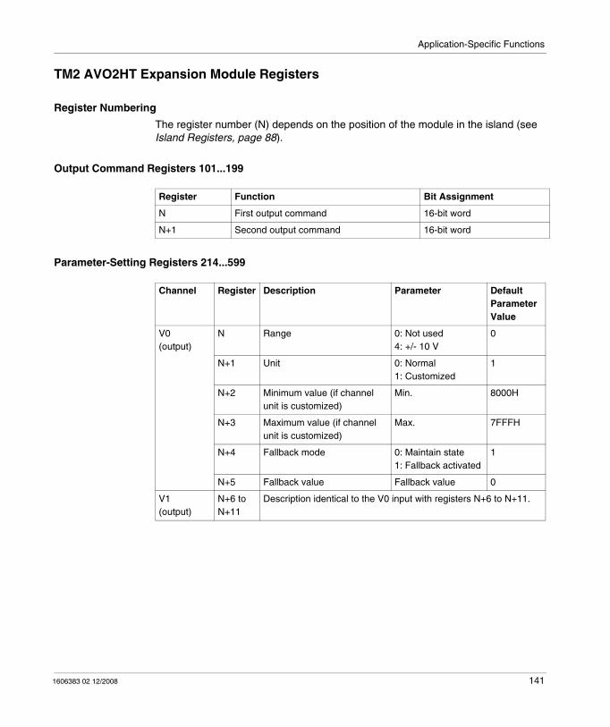
Application-Specific Functions
TM2 AVO2HT Expansion Module Registers
Register Numbering
The register number (N) depends on the position of the module in the island (see Island Registers, page 88).
Output Command Registers 101...199
Parameter-Setting Registers 214...599
Register Function Bit Assignment
N First output command 16-bit word
N+1 Second output command 16-bit word
Channel Register Description Parameter Default Parameter Value
V0(output)
N Range 0: Not used4: +/- 10 V
0
N+1 Unit 0: Normal1: Customized
1
N+2 Minimum value (if channel unit is customized)
Min. 8000H
N+3 Maximum value (if channel unit is customized)
Max. 7FFFH
N+4 Fallback mode 0: Maintain state 1: Fallback activated
1
N+5 Fallback value Fallback value 0
V1(output)
N+6 to N+11
Description identical to the V0 input with registers N+6 to N+11.
1606383 02 12/2008 141
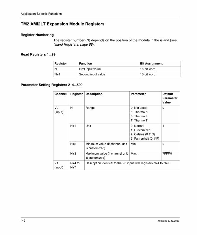
Application-Specific Functions
TM2 AMI2LT Expansion Module Registers
Register Numbering
The register number (N) depends on the position of the module in the island (see Island Registers, page 88).
Read Registers 1...99
Parameter-Setting Registers 214...599
Register Function Bit Assignment
N First input value 16-bit word
N+1 Second input value 16-bit word
Channel Register Description Parameter Default Parameter Value
V0(input)
N Range 0: Not used5: Thermo K6: Thermo J7: Thermo T
0
N+1 Unit 0: Normal1: Customized2: Celsius (0.1°C)3: Fahrenheit (0.1°F)
1
N+2 Minimum value (if channel unit is customized)
Min. 0
N+3 Maximum value (if channel unit is customized)
Max. 7FFFH
V1(input)
N+4 to N+7
Description identical to the V0 input with registers N+4 to N+7.
142 1606383 02 12/2008
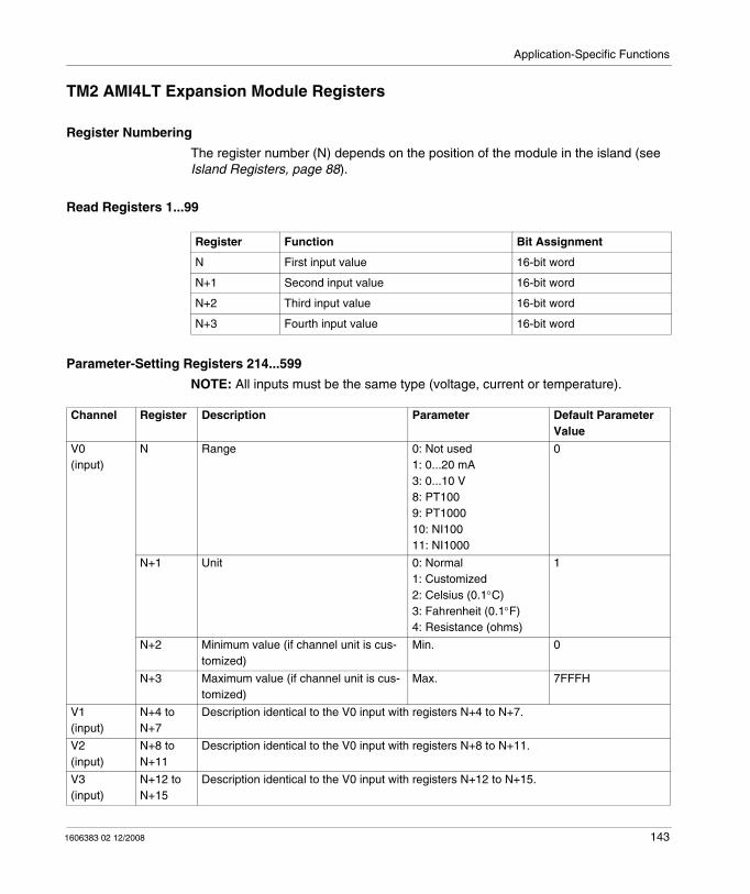
Application-Specific Functions
TM2 AMI4LT Expansion Module Registers
Register Numbering
The register number (N) depends on the position of the module in the island (see Island Registers, page 88).
Read Registers 1...99
Parameter-Setting Registers 214...599
NOTE: All inputs must be the same type (voltage, current or temperature).
Register Function Bit Assignment
N First input value 16-bit word
N+1 Second input value 16-bit word
N+2 Third input value 16-bit word
N+3 Fourth input value 16-bit word
Channel Register Description Parameter Default Parameter Value
V0(input)
N Range 0: Not used1: 0...20 mA3: 0...10 V 8: PT1009: PT100010: NI10011: NI1000
0
N+1 Unit 0: Normal1: Customized2: Celsius (0.1°C)3: Fahrenheit (0.1°F)4: Resistance (ohms)
1
N+2 Minimum value (if channel unit is cus-tomized)
Min. 0
N+3 Maximum value (if channel unit is cus-tomized)
Max. 7FFFH
V1(input)
N+4 to N+7
Description identical to the V0 input with registers N+4 to N+7.
V2(input)
N+8 to N+11
Description identical to the V0 input with registers N+8 to N+11.
V3(input)
N+12 to N+15
Description identical to the V0 input with registers N+12 to N+15.
1606383 02 12/2008 143
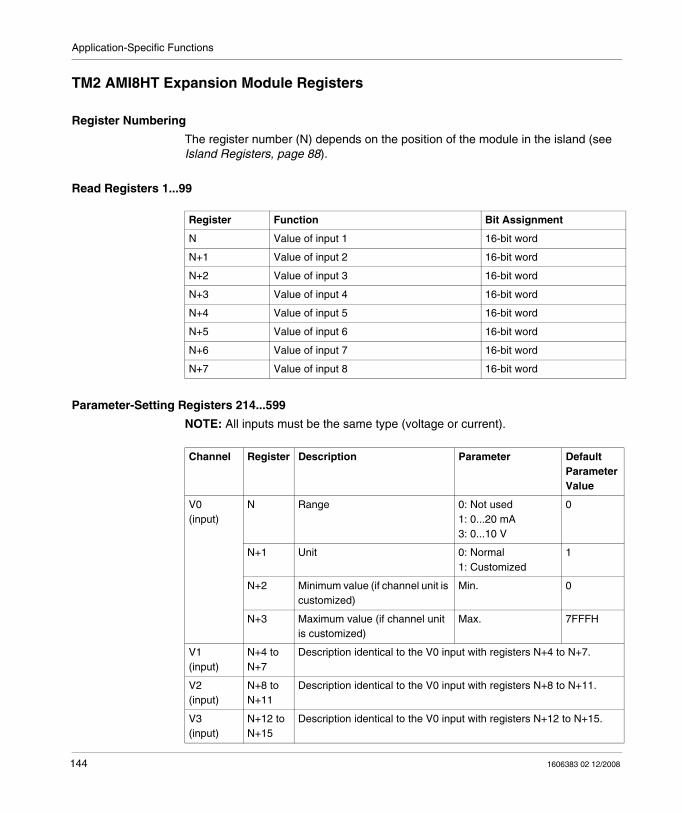
Application-Specific Functions
TM2 AMI8HT Expansion Module Registers
Register Numbering
The register number (N) depends on the position of the module in the island (see Island Registers, page 88).
Read Registers 1...99
Parameter-Setting Registers 214...599
NOTE: All inputs must be the same type (voltage or current).
Register Function Bit Assignment
N Value of input 1 16-bit word
N+1 Value of input 2 16-bit word
N+2 Value of input 3 16-bit word
N+3 Value of input 4 16-bit word
N+4 Value of input 5 16-bit word
N+5 Value of input 6 16-bit word
N+6 Value of input 7 16-bit word
N+7 Value of input 8 16-bit word
Channel Register Description Parameter Default Parameter Value
V0(input)
N Range 0: Not used1: 0...20 mA3: 0...10 V
0
N+1 Unit 0: Normal1: Customized
1
N+2 Minimum value (if channel unit is customized)
Min. 0
N+3 Maximum value (if channel unit is customized)
Max. 7FFFH
V1(input)
N+4 to N+7
Description identical to the V0 input with registers N+4 to N+7.
V2(input)
N+8 to N+11
Description identical to the V0 input with registers N+8 to N+11.
V3(input)
N+12 to N+15
Description identical to the V0 input with registers N+12 to N+15.
144 1606383 02 12/2008

Application-Specific Functions
V4(input)
N+16 to N+19
Description identical to the V0 input with registers N+16 to N+19.
V5(input)
N+20 to N+23
Description identical to the V0 input with registers N+20 to N+23.
V6(input)
N+24 to N+27
Description identical to the V0 input with registers N+24 to N+27.
V7(input)
N+28 to N+31
Description identical to the V0 input with registers N+28 to N+31.
Channel Register Description Parameter Default Parameter Value
1606383 02 12/2008 145
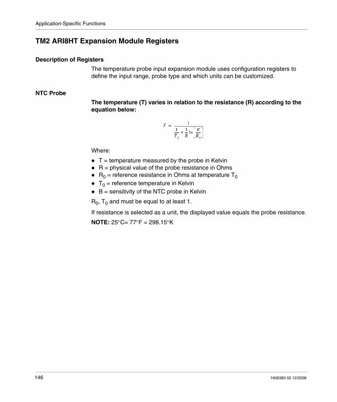
Application-Specific Functions
TM2 ARI8HT Expansion Module Registers
Description of Registers
The temperature probe input expansion module uses configuration registers to define the input range, probe type and which units can be customized.
NTC Probe
The temperature (T) varies in relation to the resistance (R) according to the equation below:
Where:
T = temperature measured by the probe in KelvinR = physical value of the probe resistance in OhmsR0 = reference resistance in Ohms at temperature T0T0 = reference temperature in KelvinB = sensitivity of the NTC probe in Kelvin
R0, T0 and must be equal to at least 1.
If resistance is selected as a unit, the displayed value equals the probe resistance.
NOTE: 25°C= 77°F = 298.15°K
146 1606383 02 12/2008
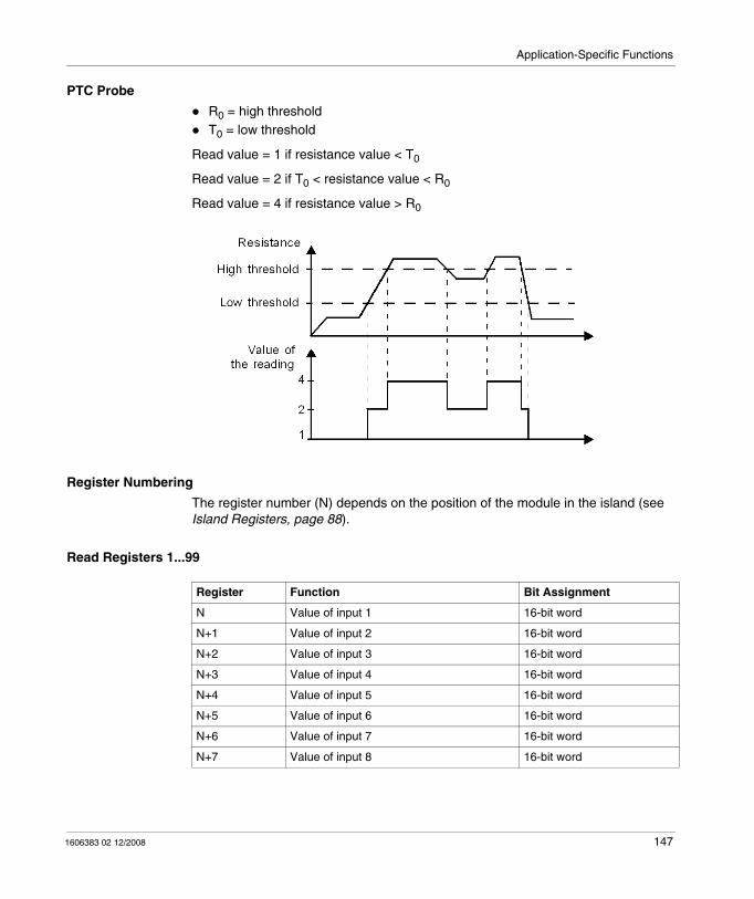
Application-Specific Functions
PTC Probe
R0 = high thresholdT0 = low threshold
Read value = 1 if resistance value < T0
Read value = 2 if T0 < resistance value < R0
Read value = 4 if resistance value > R0
Register Numbering
The register number (N) depends on the position of the module in the island (see Island Registers, page 88).
Read Registers 1...99
Register Function Bit Assignment
N Value of input 1 16-bit word
N+1 Value of input 2 16-bit word
N+2 Value of input 3 16-bit word
N+3 Value of input 4 16-bit word
N+4 Value of input 5 16-bit word
N+5 Value of input 6 16-bit word
N+6 Value of input 7 16-bit word
N+7 Value of input 8 16-bit word
1606383 02 12/2008 147

Application-Specific Functions
Parameter-Setting Registers 214...599
Channel Register Description Parameter Default Parameter Value
V0(input)
N Range 0: Not used13: NTC14: PTC
0
N+1 Unit 0 : Normal1: Customized2: Celsius (0.1°C)3: Fahrenheit (0.1°F)4: Resistance (ohms)
1
N+2 Minimum value (if channel unit is customized) Min. 0
N+3 Maximum value (if channel unit is customized) Max. 7FFFH
N+4 R0 in NTC or high threshold in PTC R0 014AH
N+5 T0 in NTC or low threshold in PTC T0 (0.01°K) 7477H
N+6 Sensitivity in NTC or ignored in PTC B (0.01°K) 0DF1H
V1(input)
N+7 to N+13
Description identical to the V0 input with registers N+7 to N+13.
V2(input)
N+14 to N+20
Description identical to the V0 input with registers N+14 to N+20.
V3(input)
N+21 to N+27
Description identical to the V0 input with registers N+21 to N+27.
V4(input)
N+28 to N+34
Description identical to the V0 input with registers N+28 to N+34.
V5(input)
N+35 to N+41
Description identical to the V0 input with registers N+35 to N+41.
V6(input)
N+42 to N+48
Description identical to the V0 input with registers N+42 to N+48.
V7(input)
N+49 to N+55
Description identical to the V0 input with registers N+49 to N+55.
148 1606383 02 12/2008
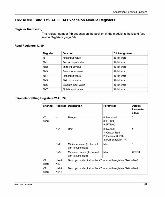
Application-Specific Functions
TM2 ARI8LT and TM2 ARI8LRJ Expansion Module Registers
Register Numbering
The register number (N) depends on the position of the module in the island (see Island Registers, page 88).
Read Registers 1...99
Parameter-Setting Registers 214...599
Register Function Bit Assignment
N First input value 16-bit word
N+1 Second input value 16-bit word
N+2 Third input value 16-bit word
N+3 Fourth input value 16-bit word
N+4 Fifth input value 16-bit word
N+5 Sixth input value 16-bit word
N+6 Seventh input value 16-bit word
N+7 Eighth input value 16-bit word
Channel Register Description Parameter Default Parameter Value
V0(input)
N Range 0: Not used8: PT1009: PT1000
0
N+1 Unit 0: Normal1: Customized2: Celsius (0.1°C)3: Fahrenheit (0.1°F)
1
N+2 Minimum value (if channel unit is customized)
Min. 0
N+3 Maximum value (if channel unit is customized)
Max. 7FFFH
V1(input)
N+4 to N+7
Description identical to the V0 input with registers N+4 to N+7.
V2(input)
N+8 to N+11
Description identical to the V0 input with registers N+8 to N+11.
1606383 02 12/2008 149

Application-Specific Functions
V3(input)
N+12 to N+15
Description identical to the V0 input with registers N+12 to N+15.
V4(input)
N+16 to N+19
Description identical to the V0 input with registers N+16 to N+19.
V5(input)
N+20 to N+23
Description identical to the V0 input with registers N+20 to N+23.
V6(input)
N+24 to N+27
Description identical to the V0 input with registers N+24 to N+27.
V7(input)
N+28 to N+31
Description identical to the V0 input with registers N+28 to N+31.
Channel Register Description Parameter Default Parameter Value
150 1606383 02 12/2008

1606383 02 12/2008
7
Software Tools
1606383 02 12/2008
Software Tools
Introduction
This chapter describes the tools and operating modes used to configure the island with Advantys Configuration Tool - LITE (FTX ES0•).
What's in this Chapter?
This chapter contains the following sections:
Section Topic Page
7.1 Introduction to Software Tools 152
7.2 Product Configuration 155
151

Software Tools
7.1 Introduction to Software Tools
Introduction
This section introduces the software tools used to install the product.
What's in this Section?
This section contains the following topics:
Topic Page
Introduction 153
Software Installation 154
152 1606383 02 12/2008

Software Tools
Introduction
General
The Advantys OTB island must be configured to operate correctly on its network.
OTB network interface modules, their I/O expansion modules and the desired I/O functions and parameters are configured using the Advantys Configuration Tool (FTX ES0•). This tool allows the user to define each OTB island and configure the parameters and the functions of the island's I/Os.
NOTE: The information that follows is a Quick start guide to configuring and using Advantys OTB network interface modules and I/O expansion modules. It is not meant to be an exhaustive description of how to set up a network.
For further information, please consult the appropriate documentation, such as network device manuals, Advantys Configuration Tool Help systems and Telemecanique product manuals, such as PL7, Unity, programmable logic controllers and so on.
1606383 02 12/2008 153

Software Tools
Software Installation
Advantys Configuration Tool, PL7, Unity
Please consult the appropriate manuals for the installation of these programming and configuration tools before installing the software.
154 1606383 02 12/2008
Software Tools
7.2 Product Configuration
Introduction
This section describes the tools and operating modes for configuring the the Advantys range of devices using the Advantys Configuration Tool (FTX ES 0•).
The device must be configured using the following steps:
Create New IslandCustomize a memory areaDownload the configuration in the device
What's in this Section?
This section contains the following topics:
Topic Page
Creating a New Island with the Advantys Configuration Tool 156
Customization of a Memory Area (Registers 1200 to 2199) 159
Downloading the Modbus Configuration 161
How to Build Configuration Files? 163
Requests with Twido Soft 166
1606383 02 12/2008 155
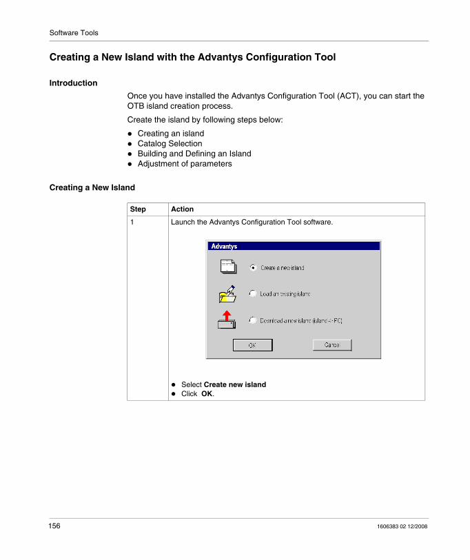
Software Tools
Creating a New Island with the Advantys Configuration Tool
Introduction
Once you have installed the Advantys Configuration Tool (ACT), you can start the OTB island creation process.
Create the island by following steps below:
Creating an islandCatalog SelectionBuilding and Defining an IslandAdjustment of parameters
Creating a New Island
Step Action
1 Launch the Advantys Configuration Tool software.
Select Create new island Click OK.
156 1606383 02 12/2008
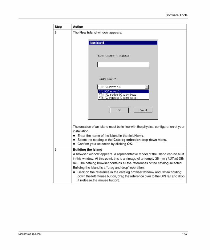
Software Tools
2 The New island window appears:
The creation of an island must be in line with the physical configuration of your installation:
Enter the name of the island in the fieldName.Select the catalog in the Catalog selection drop-down menu. Confirm your selection by clicking OK.
3 Building the IslandA browser window appears. A representative model of the island can be built in this window. At this point, this is an image of an empty 35 mm (1.37 in) DIN rail. The catalog browser contains all the references of the catalog selected. Building the island is a "drag and drop" operation:
Click on the reference in the catalog browser window and, while holding down the left mouse button, drag the reference over to the DIN rail and drop it (release the mouse button).
Step Action
1606383 02 12/2008 157

Software Tools
4 Island Configuration Once the island has been built, you can set its parameters. The parameters you need to define will depend on the I/O functions you wish to use. The islands are configured in the configuration window:
Open the configuration window by double clicking on the island or by selecting the island and then the Island/Module Editor menu.Modify the required parameter(s).Click OK to save the changes and close the configuration window.
Notes:The values given in the configuration window define the behavior of the island.Please see chapters 5, 6 and 9 of this manual for all pertinent information con-cerning the registers. The list of registers is visible in the I/O Map tab of the OTB network interface module’s configuration window.
Step Action
158 1606383 02 12/2008

Software Tools
Customization of a Memory Area (Registers 1200 to 2199)
At a Glance
The register table can be used in its default form or partially customized.
The customizable register zone is between 1200 and 1399.
This zone is accessed via registers 2000 to 2199.
Examples:
For read access to a data object configured in register 1203, you must read register 2003For read/write access to a data object configured in register 1303, you must read/write register 2103
1606383 02 12/2008 159
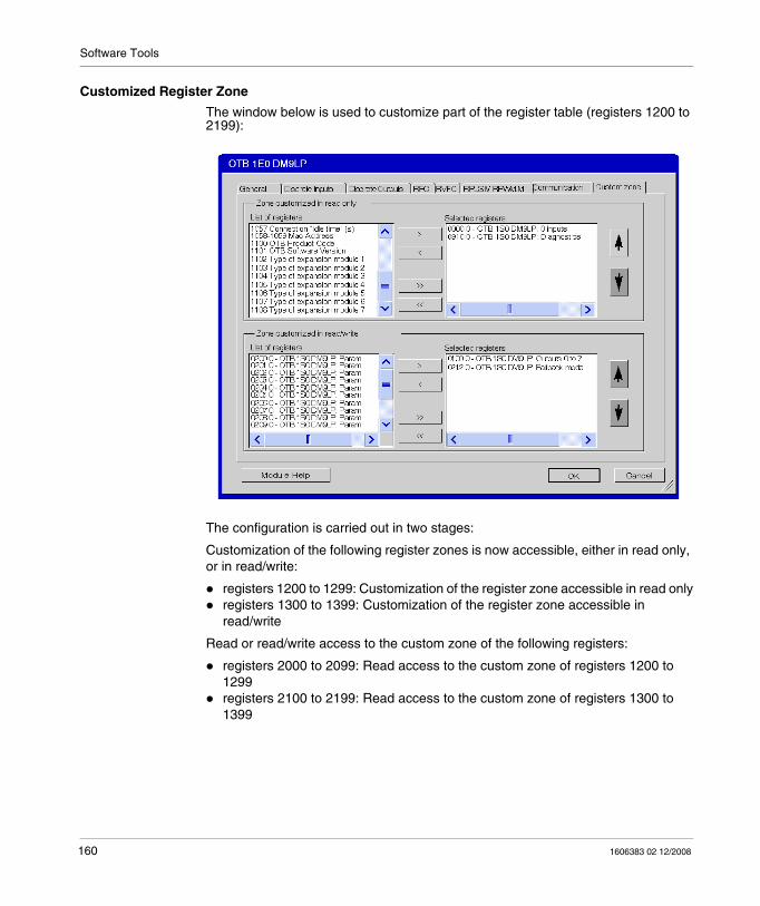
Software Tools
Customized Register Zone
The window below is used to customize part of the register table (registers 1200 to 2199):
The configuration is carried out in two stages:
Customization of the following register zones is now accessible, either in read only, or in read/write:
registers 1200 to 1299: Customization of the register zone accessible in read onlyregisters 1300 to 1399: Customization of the register zone accessible in read/write
Read or read/write access to the custom zone of the following registers:
registers 2000 to 2099: Read access to the custom zone of registers 1200 to 1299registers 2100 to 2199: Read access to the custom zone of registers 1300 to 1399
160 1606383 02 12/2008
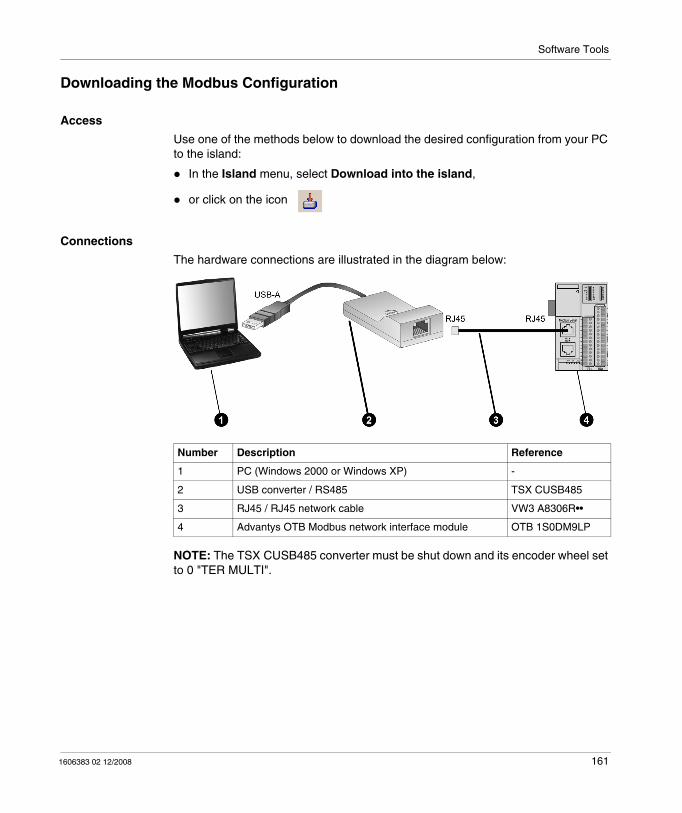
Software Tools
Downloading the Modbus Configuration
Access
Use one of the methods below to download the desired configuration from your PC to the island:
In the Island menu, select Download into the island,
or click on the icon
Connections
The hardware connections are illustrated in the diagram below:
NOTE: The TSX CUSB485 converter must be shut down and its encoder wheel set to 0 "TER MULTI".
Number Description Reference
1 PC (Windows 2000 or Windows XP) -
2 USB converter / RS485 TSX CUSB485
3 RJ45 / RJ45 network cable VW3 A8306R••
4 Advantys OTB Modbus network interface module OTB 1S0DM9LP
1606383 02 12/2008 161
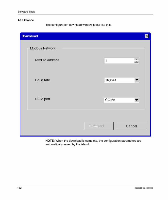
Software Tools
At a Glance
The configuration download window looks like this:
NOTE: When the download is complete, the configuration parameters are automatically saved by the island.
162 1606383 02 12/2008
Software Tools
How to Build Configuration Files?
Preliminary Steps
You will have opened an existing island or created a new island and its architecture. Before building configuration files, check that no errors have been detected. As long as there is an error displayed in the Warning window, you must modify the island architecture or the module configuration accordingly.
To see the list of errors, use one of the following methods:Select Warning from the menu,
or click on the icon
This gives access to the Warning Window (see the ACT software online help).
You can build the following files:
for Unity (Premium and M340):A symbol table and a function block (DFB) for configuring the island.for Twido:A symbol table and a subroutine (LIST) for configuring the island.
Procedure
To build the configuration file:
Step Action
1 Launch the configuration file build process by using one of the following methods:
Click on the icon
Use the Build menu
1606383 02 12/2008 163
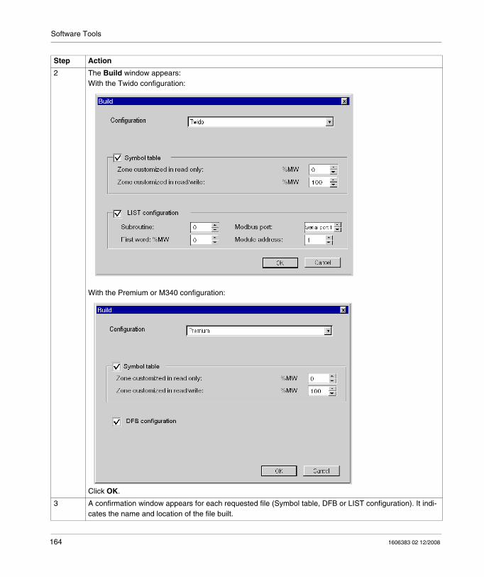
Software Tools
2 The Build window appears:With the Twido configuration:
With the Premium or M340 configuration:
Click OK.
3 A confirmation window appears for each requested file (Symbol table, DFB or LIST configuration). It indi-cates the name and location of the file built.
Step Action
164 1606383 02 12/2008

Software Tools
Configuration Files
Configuration files are the files created when an island is generated.
These files are created:In the directory defined in user preferences,With the same name as the island.
When used with Twido, the LIST configuration is built in a TXT file.
When used with Unity (Premium or M340), the DFB configuration is built in an .XDB file.
Symbol Table
When used with Twido, the symbol table is built in a .CSV file.
When used with Unity (Premium or M340), the symbol table is built in an .XSY file.
These files are created:In the directory defined in user preferences,With the same name as the island.
1606383 02 12/2008 165
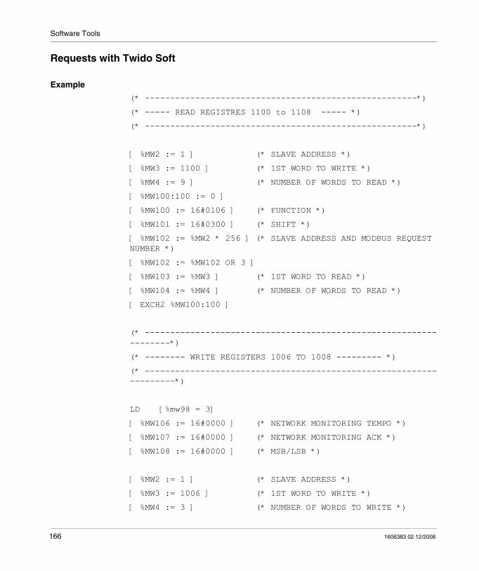
Software Tools
Requests with Twido Soft
Example
(* ------------------------------------------------------*)
(* ----- READ REGISTRES 1100 to 1108 ----- *)
(* ------------------------------------------------------*)
[ %MW2 := 1 ] (* SLAVE ADDRESS *)
[ %MW3 := 1100 ] (* 1ST WORD TO WRITE *)
[ %MW4 := 9 ] (* NUMBER OF WORDS TO READ *)
[ %MW100:100 := 0 ]
[ %MW100 := 16#0106 ] (* FUNCTION *)
[ %MW101 := 16#0300 ] (* SHIFT *)
[ %MW102 := %MW2 * 256 ] (* SLAVE ADDRESS AND MODBUS REQUEST NUMBER *)
[ %MW102 := %MW102 OR 3 ]
[ %MW103 := %MW3 ] (* 1ST WORD TO READ *)
[ %MW104 := %MW4 ] (* NUMBER OF WORDS TO READ *)
[ EXCH2 %MW100:100 ]
(* ------------------------------------------------------------------*)
(* -------- WRITE REGISTERS 1006 TO 1008 --------- *)
(* -------------------------------------------------------------------*)
LD [%mw98 = 3]
[ %MW106 := 16#0000 ] (* NETWORK MONITORING TEMPO *)
[ %MW107 := 16#0000 ] (* NETWORK MONITORING ACK *)
[ %MW108 := 16#0000 ] (* MSB/LSB *)
[ %MW2 := 1 ] (* SLAVE ADDRESS *)
[ %MW3 := 1006 ] (* 1ST WORD TO WRITE *)
[ %MW4 := 3 ] (* NUMBER OF WORDS TO WRITE *)
166 1606383 02 12/2008

Software Tools
[ %MW100:4 := 0 ]
[ %MW100 := %MW4 * 2 ] (* LENGTH TO SEND *)
[ %MW100 := %MW100 + 16#0108 ] (* 16#0108 FUNCTION *)
[ %MW101 := 16#0007 ] (* SHIFT *)
[ %MW102 := %MW2 * 256 ] (* SLAVE @ AND MODBUS REQUEST *)
[ %MW102 := %MW102 OR 16 ]
[ %MW103 := %MW3 ] (* 1ST WORD TO WRITE *)
[ %MW104 := %MW4 ] (* NUMBER OF WORDS TO WRITE *)
[ %MW105 := %MW4 * 2 ] (* NUMBER OF BYTES TO WRITE *)
[ EXCH2 %MW100:100 ] (* SEND REQUEST *)
1606383 02 12/2008 167

Software Tools
168 1606383 02 12/2008

1606383 02 12/2008
8
Diagnostics
1606383 02 12/2008
Diagnostics of the Advantys OTB Island
At a Glance
The Advantys OTB diagnostics function can be used to analyze the behavior of modules:
The LEDs indicate the communication and I/O status,At a Glance
What's in this Chapter?
This chapter contains the following topics:
Topic Page
Indicator Lights (LEDs) 170
OTB Island Diagnostic Registers 172
Behavior in the Event of a Fault 177
169
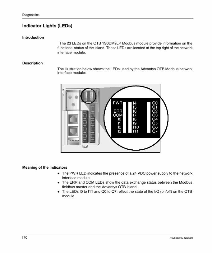
Diagnostics
Indicator Lights (LEDs)
Introduction
The 23 LEDs on the OTB 1S0DM9LP Modbus module provide information on the functional status of the island. These LEDs are located at the top right of the network interface module.
Description
The illustration below shows the LEDs used by the Advantys OTB Modbus network interface module:
Meaning of the Indicators
The PWR LED indicates the presence of a 24 VDC power supply to the network interface module.The ERR and COM LEDs show the data exchange status between the Modbus fieldbus master and the Advantys OTB island.The LEDs I0 to I11 and Q0 to Q7 reflect the state of the I/O (on/off) on the OTB module.
170 1606383 02 12/2008
Diagnostics
Modbus Communication LEDs
The table below describes the conditions of and the colors used by the COM and ERR LEDs to display the normal operating modes and error conditions of an Advantys OTB Modbus network interface module.
I/O Status Indicators
The table below describes the conditions of and the colors used by the PWR, I0 to I11 and Q0 to Q7 LEDs to display the normal operating modes and error conditions for the Advantys OTB Modbus network interface module power supply and I/O.
Name LED Color Type of flashing Function
Com (communication) yellow random flashing On when sending and receiving
Err (error)
red on Internal error
random flashing Other errors: communication errors or configuration fault
Name LED Color Status Function
PWR (power)
green on 24 VDC present on the OTB module
I0 to I11
green on Input at 24 V
off Input at 0 V
Q0 to Q7 green on Output at 24 V or contact closed
off Output at 0 V or contact open
1606383 02 12/2008 171

Diagnostics
OTB Island Diagnostic Registers
Overview
The diagnostics use Registers 900...917. All the parameters in this zone can only be accessed in read mode.
Registers 900 and 901:
Island status:
NOTE:
Bit values:0: No fault1: Fault present
Registers Function Description
900 Island status word
Bits [0...8]: Not usedBit [9]: Communication fault or external faultBits [10...12]: Not usedBit [13]: Configuration fault (expansion modules missing or in-correctly configured)Bits [14...15]: Not used
901 Expansion module status word
Bit [0]: Status of communication moduleBit [1]: Status of first expansion moduleBit [2]: Status of second expansion moduleBit [3]: Status of third expansion moduleBit [4]: Status of fourth expansion moduleBit [5]: Status of fifth expansion moduleBit [6]: Status of sixth expansion moduleBit [7]: Status of seventh expansion module
172 1606383 02 12/2008
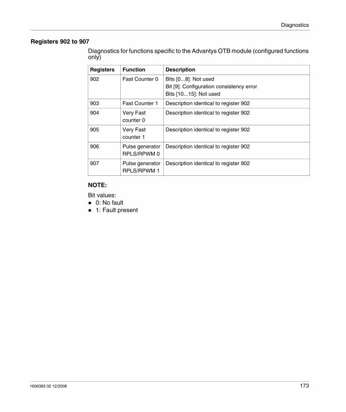
Diagnostics
Registers 902 to 907
Diagnostics for functions specific to the Advantys OTB module (configured functions only)
NOTE:
Bit values:0: No fault1: Fault present
Registers Function Description
902 Fast Counter 0 Bits [0...8]: Not usedBit [9]: Configuration consistency error Bits [10...15]: Not used
903 Fast Counter 1 Description identical to register 902
904 Very Fast counter 0
Description identical to register 902
905 Very Fast counter 1
Description identical to register 902
906 Pulse generator RPLS/RPWM 0
Description identical to register 902
907 Pulse generator RPLS/RPWM 1
Description identical to register 902
1606383 02 12/2008 173
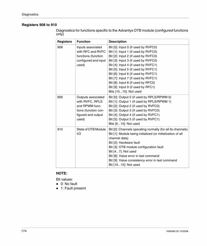
Diagnostics
Registers 908 to 910
Diagnostics for functions specific to the Advantys OTB module (configured functions only)
NOTE:
Bit values:0: No fault1: Fault present
Registers Function Description
908 Inputs associated with RFC and RVFC functions (function configured and input used)
Bit [0]: Input 0 (if used by RVFC0)Bit [1]: Input 1 (if used by RVFC0)Bit [2]: Input 2 (if used by RVFC0)Bit [3]: Input 3 (if used by RVFC0)Bit [4]: Input 4 (if used by RVFC1)Bit [5]: Input 5 (if used by RVFC1)Bit [6]: Input 6 (if used by RVFC1)Bit [7]: Input 7 (if used by RVFC1)Bit [8]: Input 8 (if used by RFC0)Bit [9]: Input 9 (if used by RFC1)Bits [10...15]: Not used
909 Outputs associated with RVFC, RPLS and RPWM func-tions (function con-figured and output used)
Bit [0]: Output 0 (if used by RPLS/RPWM 0)Bit [1]: Output 1 (if used by RPLS/RPWM 1)Bit [2]: Output 2 (if used by RVFC0)Bit [3]: Output 3 (if used by RVFC0)Bit [4]: Output 4 (if used by RVFC1)Bit [5]: Output 5 (if used by RVFC1)Bits [6...15]: Not used
910 State of OTB Module I/O
Bit [0]: Channels operating normally (for all its channels)Bit [1]: Module being initialized (or initialization of all channel data)Bit [2]: Hardware faultBit [3]: OTB module configuration faultBit [4...7]: Not usedBit [8]: Value error in last commandBit [9]: Value consistency error in last commandBit [10...15]: Not used
174 1606383 02 12/2008
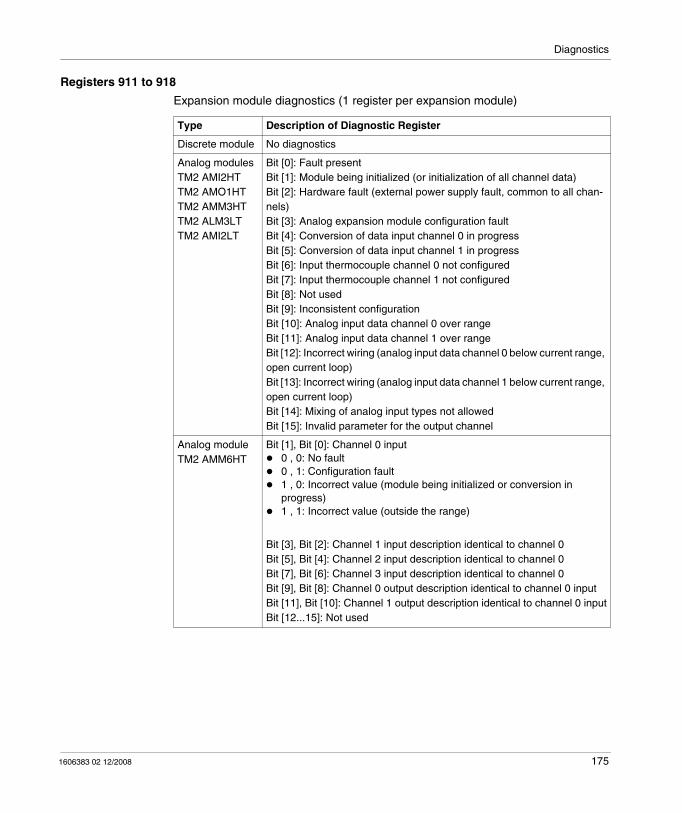
Diagnostics
Registers 911 to 918
Expansion module diagnostics (1 register per expansion module)
Type Description of Diagnostic Register
Discrete module No diagnostics
Analog modulesTM2 AMI2HTTM2 AMO1HTTM2 AMM3HTTM2 ALM3LTTM2 AMI2LT
Bit [0]: Fault presentBit [1]: Module being initialized (or initialization of all channel data)Bit [2]: Hardware fault (external power supply fault, common to all chan-nels)Bit [3]: Analog expansion module configuration faultBit [4]: Conversion of data input channel 0 in progressBit [5]: Conversion of data input channel 1 in progressBit [6]: Input thermocouple channel 0 not configuredBit [7]: Input thermocouple channel 1 not configuredBit [8]: Not usedBit [9]: Inconsistent configurationBit [10]: Analog input data channel 0 over rangeBit [11]: Analog input data channel 1 over rangeBit [12]: Incorrect wiring (analog input data channel 0 below current range, open current loop)Bit [13]: Incorrect wiring (analog input data channel 1 below current range, open current loop)Bit [14]: Mixing of analog input types not allowedBit [15]: Invalid parameter for the output channel
Analog moduleTM2 AMM6HT
Bit [1], Bit [0]: Channel 0 input0 , 0: No fault0 , 1: Configuration fault1 , 0: Incorrect value (module being initialized or conversion in progress)1 , 1: Incorrect value (outside the range)
Bit [3], Bit [2]: Channel 1 input description identical to channel 0Bit [5], Bit [4]: Channel 2 input description identical to channel 0Bit [7], Bit [6]: Channel 3 input description identical to channel 0Bit [9], Bit [8]: Channel 0 output description identical to channel 0 inputBit [11], Bit [10]: Channel 1 output description identical to channel 0 inputBit [12...15]: Not used
1606383 02 12/2008 175
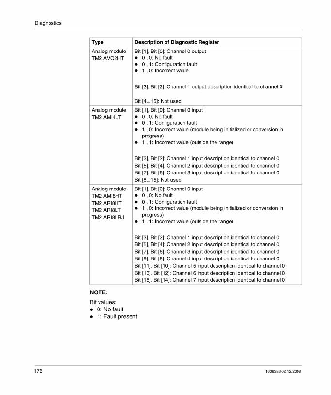
Diagnostics
NOTE:
Bit values:0: No fault1: Fault present
Analog moduleTM2 AVO2HT
Bit [1], Bit [0]: Channel 0 output0 , 0: No fault0 , 1: Configuration fault1 , 0: Incorrect value
Bit [3], Bit [2]: Channel 1 output description identical to channel 0
Bit [4...15]: Not used
Analog moduleTM2 AMI4LT
Bit [1], Bit [0]: Channel 0 input0 , 0: No fault0 , 1: Configuration fault1 , 0: Incorrect value (module being initialized or conversion in progress)1 , 1: Incorrect value (outside the range)
Bit [3], Bit [2]: Channel 1 input description identical to channel 0Bit [5], Bit [4]: Channel 2 input description identical to channel 0Bit [7], Bit [6]: Channel 3 input description identical to channel 0Bit [8...15]: Not used
Analog moduleTM2 AMI8HTTM2 ARI8HTTM2 ARI8LTTM2 ARI8LRJ
Bit [1], Bit [0]: Channel 0 input0 , 0: No fault0 , 1: Configuration fault1 , 0: Incorrect value (module being initialized or conversion in progress)1 , 1: Incorrect value (outside the range)
Bit [3], Bit [2]: Channel 1 input description identical to channel 0Bit [5], Bit [4]: Channel 2 input description identical to channel 0Bit [7], Bit [6]: Channel 3 input description identical to channel 0Bit [9], Bit [8]: Channel 4 input description identical to channel 0Bit [11], Bit [10]: Channel 5 input description identical to channel 0Bit [13], Bit [12]: Channel 6 input description identical to channel 0Bit [15], Bit [14]: Channel 7 input description identical to channel 0
Type Description of Diagnostic Register
176 1606383 02 12/2008
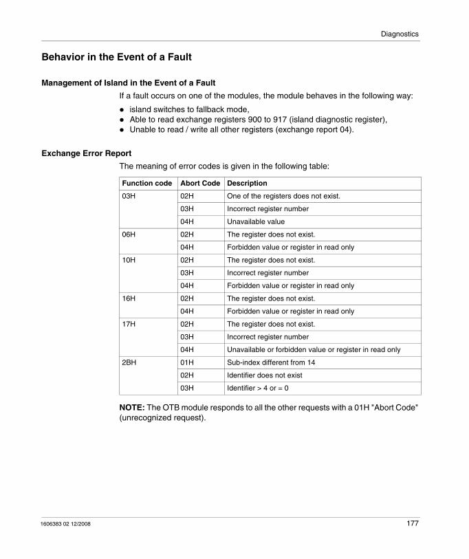
Diagnostics
Behavior in the Event of a Fault
Management of Island in the Event of a Fault
If a fault occurs on one of the modules, the module behaves in the following way:
island switches to fallback mode,Able to read exchange registers 900 to 917 (island diagnostic register),Unable to read / write all other registers (exchange report 04).
Exchange Error Report
The meaning of error codes is given in the following table:
NOTE: The OTB module responds to all the other requests with a 01H "Abort Code" (unrecognized request).
Function code Abort Code Description
03H 02H One of the registers does not exist.
03H Incorrect register number
04H Unavailable value
06H 02H The register does not exist.
04H Forbidden value or register in read only
10H 02H The register does not exist.
03H Incorrect register number
04H Forbidden value or register in read only
16H 02H The register does not exist.
04H Forbidden value or register in read only
17H 02H The register does not exist.
03H Incorrect register number
04H Unavailable or forbidden value or register in read only
2BH 01H Sub-index different from 14
02H Identifier does not exist
03H Identifier > 4 or = 0
1606383 02 12/2008 177

Diagnostics
178 1606383 02 12/2008
1606383 02 12/2008
9
Mapping
1606383 02 12/2008
Island Registers Table
Registers Table
This chapter provides the registers table for the Advantys OTB network interface module and expansion modules. The table is divided up into data zones and provides a map of the island (mapping).
What's in this Chapter?
This chapter contains the following topics:
Topic Page
Registers Table (mapping) for Modbus Advantys OTB Module 180
I/O Registers 182
Application-Specific Function Registers 184
Diagnostic Registers 188
Island Management Registers 193
Customized Zone Registers 195
Island Module Identification Registers 196
179
Mapping
Registers Table (mapping) for Modbus Advantys OTB Module
At a Glance
The registers table depends on the network interface module, the connected expansion modules and the type of those modules. Specific register zones are reserved for different types of data.
NOTE: The numerical values shown in the tables below are either in decimal (value only), or in hexadecimal (value followed by H).
Register Table (mapping)
The two following tables show the two OTB register zones corresponding to the supported functions:
The manufacturer zoneThe custom zone
The manufacturer zone provides all the data available on status and features of the island. The registers are defined when the island is powered up. The number and order of the available registers is defined by the expansion modules added to the OTB module from left to right.
NOTE: The available registers are the registers corresponding to existing modules.
The customized zone enables you to organize data so as to optimize exchanges between the master and the island while assembling non contiguous registers in a contiguous register table. This reduces the number of Modbus read/write instructions.
Zone Register Function Page
Manufac-turer zone
0...99 Status of island inputs 0...99 (see page 182)
100...199 Island output commands 100...199 (see page 182)
200...599 Island I/O configuration parameters 200...599 (see page 183)
600...699 Remote Fast Counter (RFC) function 600...699 (see page 184)
700...799 Remote Very Fast Counter (RVFC) function 700...799 (see page 185)
800...899 Remote Pulse Generator function (RPLS)Remote pulse generator function with pulse width modulation (RPWM)
800...899 (see page 187)
900...999 Island diagnostics 900...999 (see page 188)
1000...1099 Management of module behavior 1000...1099 (see page 193)
1100...1108 Description of modules constituting the is-land
1100...1108 (see page 196)
180 1606383 02 12/2008

Mapping
The customized zone is configured in the definition zone:
The definition zones (1200...1299 and 1300...1399) contain the register numbers of accessible data. The customized zones (2000...2099 and 2100...2199) give access to the definition zones.
Example:
If register 1200 has a value of 0, register 2000 will have the same content as register 0.If register 1300 has a value of 100, the write data in register 2100 will have the same effect as the write data in register 100.
NOTE: The customized zone can only contain registers available in the manufacturer zone.
Zone Register Function Page
Definition zones
1200...1299 Customization of the register zone acces-sible in read only
1200...1299 (see page 195)
1300...1399 Customization of the register zone acces-sible in read/write
1300...1399 (see page 195)
Customized zones
2000...2099 Read access to the custom zone of regis-ters 1200 to 1299
2000...2099 (see page 195)
2100...2199 Read/write access to the custom zone of registers 1300 to 1399
2100...2199 (see page 195)
1606383 02 12/2008 181
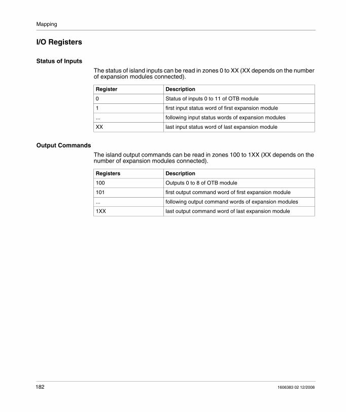
Mapping
I/O Registers
Status of Inputs
The status of island inputs can be read in zones 0 to XX (XX depends on the number of expansion modules connected).
Output Commands
The island output commands can be read in zones 100 to 1XX (XX depends on the number of expansion modules connected).
Register Description
0 Status of inputs 0 to 11 of OTB module
1 first input status word of first expansion module
... following input status words of expansion modules
XX last input status word of last expansion module
Registers Description
100 Outputs 0 to 8 of OTB module
101 first output command word of first expansion module
... following output command words of expansion modules
1XX last output command word of last expansion module
182 1606383 02 12/2008
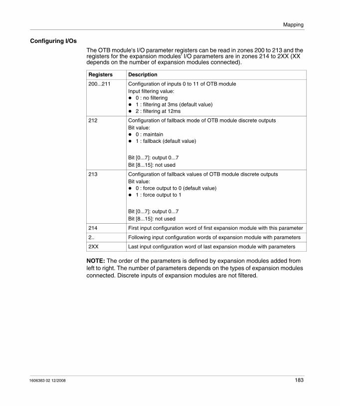
Mapping
Configuring I/Os
The OTB module's I/O parameter registers can be read in zones 200 to 213 and the registers for the expansion modules' I/O parameters are in zones 214 to 2XX (XX depends on the number of expansion modules connected).
NOTE: The order of the parameters is defined by expansion modules added from left to right. The number of parameters depends on the types of expansion modules connected. Discrete inputs of expansion modules are not filtered.
Registers Description
200...211 Configuration of inputs 0 to 11 of OTB moduleInput filtering value:
0 : no filtering1 : filtering at 3ms (default value)2 : filtering at 12ms
212 Configuration of fallback mode of OTB module discrete outputsBit value:
0 : maintain1 : fallback (default value)
Bit [0...7]: output 0...7Bit [8...15]: not used
213 Configuration of fallback values of OTB module discrete outputsBit value:
0 : force output to 0 (default value)1 : force output to 1
Bit [0...7]: output 0...7Bit [8...15]: not used
214 First input configuration word of first expansion module with this parameter
2.. Following input configuration words of expansion module with parameters
2XX Last input configuration word of last expansion module with parameters
1606383 02 12/2008 183
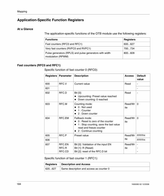
Mapping
Application-Specific Function Registers
At a Glance
The application-specific functions of the OTB module use the following registers:
Fast counters (RFC0 and RFC1)
Specific function of fast counter 0 (RFC0):
Specific function of fast counter 1 (RFC1):
Functions Registers
Fast counters (RFC0 and RFC1) 600...627
Very fast counters (RVFC0 and RVFC1) 700...734
Pulse generators (RPLS) and pulse generators with width modulation (RPWM)
800...828
Registers Parameter Description Access Default value
600 RFC.V Current value Read -
601 -
602 RFC.D Bit [0]: Upcounting: Preset value reachedDown counting: 0 reached
Read -
603 RFC.M Counting mode:0 : Not used1 : Counter2 : Down counter
Read/Write
0
604 RFC.EM Fallback mode:0 : Reset to zero of the counter1 : Stop counting, save the last value read and freeze counter 2 : Continue counting
Read/Write
0
605 RFC.P Preset value Read/Write
FFFFH
606 FFFFH
607 RFC.ENRFC.RRFC.CD
Bit [0]: Validation of the input ENBit [1]: R (Reset)Bit [2]: reset of the RFC.D bit
Read/Write
---
Registers Description and Access
620...627 Same description and access as counter 0
184 1606383 02 12/2008
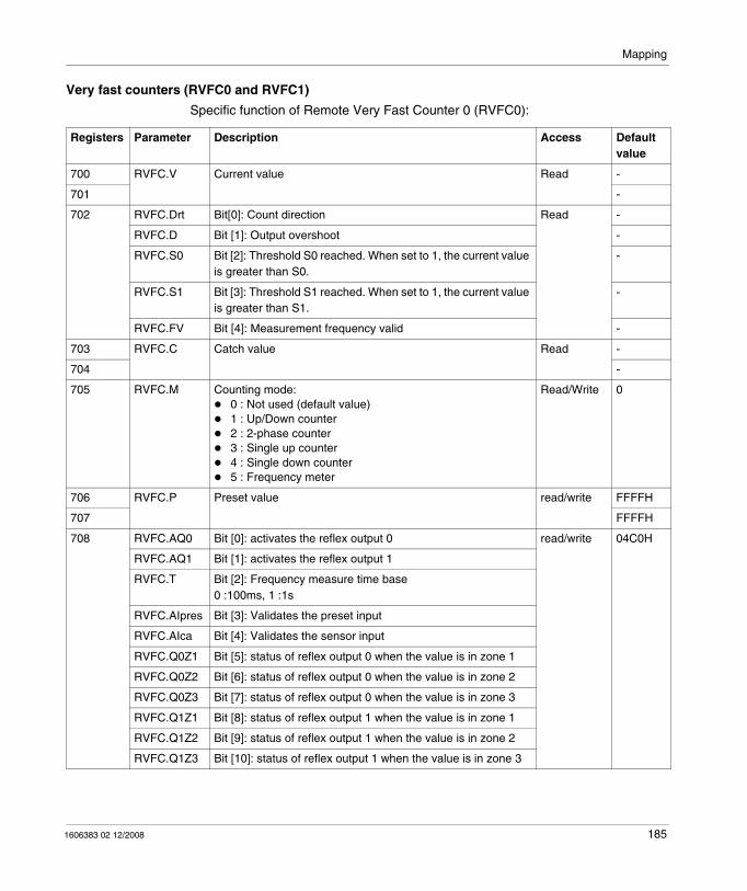
Mapping
Very fast counters (RVFC0 and RVFC1)
Specific function of Remote Very Fast Counter 0 (RVFC0):
Registers Parameter Description Access Default value
700 RVFC.V Current value Read -
701 -
702 RVFC.Drt Bit[0]: Count direction Read -
RVFC.D Bit [1]: Output overshoot -
RVFC.S0 Bit [2]: Threshold S0 reached. When set to 1, the current value is greater than S0.
-
RVFC.S1 Bit [3]: Threshold S1 reached. When set to 1, the current value is greater than S1.
-
RVFC.FV Bit [4]: Measurement frequency valid -
703 RVFC.C Catch value Read -
704 -
705 RVFC.M Counting mode:0 : Not used (default value)1 : Up/Down counter2 : 2-phase counter3 : Single up counter4 : Single down counter5 : Frequency meter
Read/Write 0
706 RVFC.P Preset value read/write FFFFH
707 FFFFH
708 RVFC.AQ0 Bit [0]: activates the reflex output 0 read/write 04C0H
RVFC.AQ1 Bit [1]: activates the reflex output 1
RVFC.T Bit [2]: Frequency measure time base0 :100ms, 1 :1s
RVFC.AIpres Bit [3]: Validates the preset input
RVFC.AIca Bit [4]: Validates the sensor input
RVFC.Q0Z1 Bit [5]: status of reflex output 0 when the value is in zone 1
RVFC.Q0Z2 Bit [6]: status of reflex output 0 when the value is in zone 2
RVFC.Q0Z3 Bit [7]: status of reflex output 0 when the value is in zone 3
RVFC.Q1Z1 Bit [8]: status of reflex output 1 when the value is in zone 1
RVFC.Q1Z2 Bit [9]: status of reflex output 1 when the value is in zone 2
RVFC.Q1Z3 Bit [10]: status of reflex output 1 when the value is in zone 3
1606383 02 12/2008 185
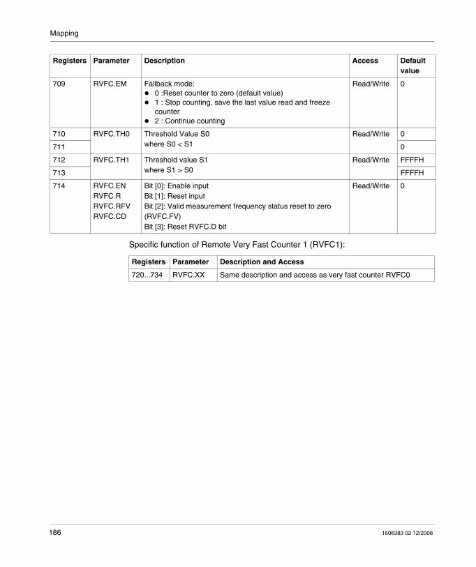
Mapping
Specific function of Remote Very Fast Counter 1 (RVFC1):
709 RVFC.EM Fallback mode:0 :Reset counter to zero (default value)1 : Stop counting, save the last value read and freeze counter 2 : Continue counting
Read/Write 0
710 RVFC.TH0 Threshold Value S0where S0 < S1
Read/Write 0
711 0
712 RVFC.TH1 Threshold value S1where S1 > S0
Read/Write FFFFH
713 FFFFH
714 RVFC.ENRVFC.RRVFC.RFVRVFC.CD
Bit [0]: Enable inputBit [1]: Reset inputBit [2]: Valid measurement frequency status reset to zero (RVFC.FV)Bit [3]: Reset RVFC.D bit
Read/Write 0
Registers Parameter Description Access Default value
Registers Parameter Description and Access
720...734 RVFC.XX Same description and access as very fast counter RVFC0
186 1606383 02 12/2008
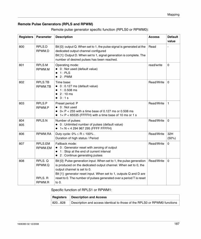
Mapping
Remote Pulse Generators (RPLS and RPWM)
Remote pulse generator specific function (RPLS0 or RPWM0):
Specific function of RPLS1 or RPWM1:
Registers Parameter Description Access Default value
800 RPLS.DRPWM.D
Bit [0]: output Q. When set to 1, the pulse signal is generated at the dedicated output channel configured Bit [1]: Output D. When set to 1, signal generation is complete. The number of desired pulses has been reached.
Read -
801 RPLS.M RPWM.M
Operating mode:0 : Not used (default value)1 : PLS2 : PWM
read/write 0
802 RPLS.TBRPWM.TB
Time base:0 : 0.127 ms (default value)1 : 0.508 ms2 : 10 ms3 : 1 s
Read/Write 0
803 RPLS.PRPWM.P
Preset period: P0 : Not used0< P < 255 with a time base of 0.127 ms or 0.508 ms1< P < 65535 (FFFFH) with a time base of 10 ms or 1 s
Read/Write 1
804805
RPLS.N Number of pulses:0 : Unlimited number of pulses (default value)1< N < 4 294 967 295 (FFFF FFFFH)
Read/Write 0
806 RPWM.RA Duty cycle: 0% ≤ R ≤ 100% .Duration of high status / Period
Read/Write 32H (50%)
807 RPLS.EMRPWM.EM
Fallback mode:0 : Generator reset with zeroing of output1 : Stop at the end of current interval2 : Continue generating pulses
Read/Write 0
808 RPLS. QRPWM.Q
RPLS. RRPWM.R
Bit [0]: Pulse generation input. When set to 1, the pulse generation is produced on the dedicated output channel. When set to 0, the output channel is set to 0. Bit [1]: generator reset input. When set to 1, outputs Q and D are reset to 0. The number of pulses generated over a period T is reset to 0.
Read/Write 0
Registers Description and Access
820...828 Description and access identical to those of the RPLS0 or RPWM0 functions
1606383 02 12/2008 187

Mapping
Diagnostic Registers
Introduction
The diagnostic registers can only be accessed in read mode.
Registers 900 and 901
Registers 900 and 901: Island status
NOTE:
Bit values:0: No fault1: Fault present
Registers Function Description
900 Island status word
Bits [0...8]: Not usedBit [9]: Communication fault or external faultBits [10...12]: Not usedBit [13]: Configuration fault (expansion modules missing or incorrectly configured)Bits [14...15]: Not used
901 Expansion module status word
Bit [0]: Network interface module statusBit [1]: Status of first expansion moduleBit [2]: Status of second expansion moduleBit [3]: Status of third expansion moduleBit [4]: Status of fourth expansion moduleBit [5]: Status of fifth expansion moduleBit [6]: Status of sixth expansion moduleBit [7]: Status of seventh expansion module
188 1606383 02 12/2008
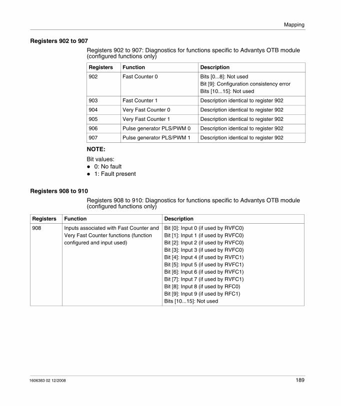
Mapping
Registers 902 to 907
Registers 902 to 907: Diagnostics for functions specific to Advantys OTB module (configured functions only)
NOTE:
Bit values:0: No fault1: Fault present
Registers 908 to 910
Registers 908 to 910: Diagnostics for functions specific to Advantys OTB module (configured functions only)
Registers Function Description
902 Fast Counter 0 Bits [0...8]: Not usedBit [9]: Configuration consistency error Bits [10...15]: Not used
903 Fast Counter 1 Description identical to register 902
904 Very Fast Counter 0 Description identical to register 902
905 Very Fast Counter 1 Description identical to register 902
906 Pulse generator PLS/PWM 0 Description identical to register 902
907 Pulse generator PLS/PWM 1 Description identical to register 902
Registers Function Description
908 Inputs associated with Fast Counter and Very Fast Counter functions (function configured and input used)
Bit [0]: Input 0 (if used by RVFC0)Bit [1]: Input 1 (if used by RVFC0)Bit [2]: Input 2 (if used by RVFC0)Bit [3]: Input 3 (if used by RVFC0)Bit [4]: Input 4 (if used by RVFC1)Bit [5]: Input 5 (if used by RVFC1)Bit [6]: Input 6 (if used by RVFC1)Bit [7]: Input 7 (if used by RVFC1)Bit [8]: Input 8 (if used by RFC0)Bit [9]: Input 9 (if used by RFC1)Bits [10...15]: Not used
1606383 02 12/2008 189
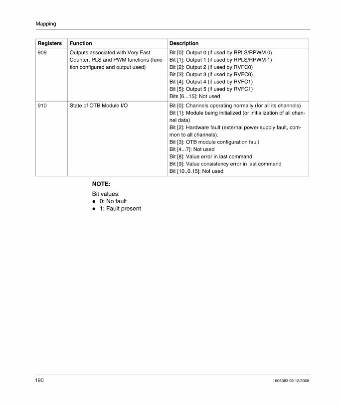
Mapping
NOTE:
Bit values:0: No fault1: Fault present
909 Outputs associated with Very Fast Counter, PLS and PWM functions (func-tion configured and output used)
Bit [0]: Output 0 (if used by RPLS/RPWM 0)Bit [1]: Output 1 (if used by RPLS/RPWM 1)Bit [2]: Output 2 (if used by RVFC0)Bit [3]: Output 3 (if used by RVFC0)Bit [4]: Output 4 (if used by RVFC1)Bit [5]: Output 5 (if used by RVFC1)Bits [6...15]: Not used
910 State of OTB Module I/O Bit [0]: Channels operating normally (for all its channels)Bit [1]: Module being initialized (or initialization of all chan-nel data)Bit [2]: Hardware fault (external power supply fault, com-mon to all channels).Bit [3]: OTB module configuration faultBit [4...7]: Not usedBit [8]: Value error in last commandBit [9]: Value consistency error in last commandBit [10..0.15]: Not used
Registers Function Description
190 1606383 02 12/2008
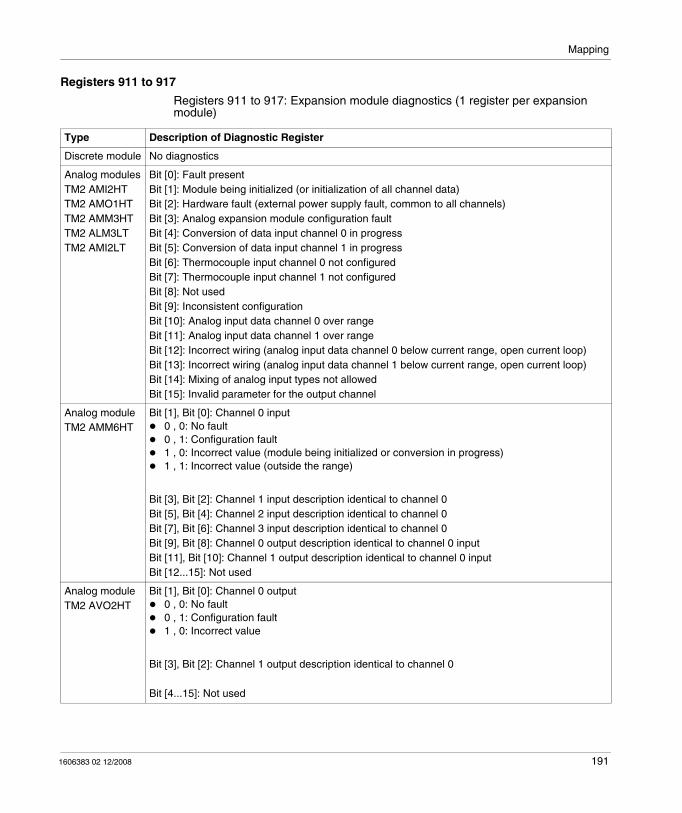
Mapping
Registers 911 to 917
Registers 911 to 917: Expansion module diagnostics (1 register per expansion module)
Type Description of Diagnostic Register
Discrete module No diagnostics
Analog modulesTM2 AMI2HTTM2 AMO1HTTM2 AMM3HTTM2 ALM3LTTM2 AMI2LT
Bit [0]: Fault presentBit [1]: Module being initialized (or initialization of all channel data)Bit [2]: Hardware fault (external power supply fault, common to all channels)Bit [3]: Analog expansion module configuration faultBit [4]: Conversion of data input channel 0 in progressBit [5]: Conversion of data input channel 1 in progressBit [6]: Thermocouple input channel 0 not configuredBit [7]: Thermocouple input channel 1 not configuredBit [8]: Not usedBit [9]: Inconsistent configurationBit [10]: Analog input data channel 0 over rangeBit [11]: Analog input data channel 1 over rangeBit [12]: Incorrect wiring (analog input data channel 0 below current range, open current loop)Bit [13]: Incorrect wiring (analog input data channel 1 below current range, open current loop)Bit [14]: Mixing of analog input types not allowedBit [15]: Invalid parameter for the output channel
Analog moduleTM2 AMM6HT
Bit [1], Bit [0]: Channel 0 input0 , 0: No fault0 , 1: Configuration fault1 , 0: Incorrect value (module being initialized or conversion in progress)1 , 1: Incorrect value (outside the range)
Bit [3], Bit [2]: Channel 1 input description identical to channel 0Bit [5], Bit [4]: Channel 2 input description identical to channel 0Bit [7], Bit [6]: Channel 3 input description identical to channel 0Bit [9], Bit [8]: Channel 0 output description identical to channel 0 inputBit [11], Bit [10]: Channel 1 output description identical to channel 0 inputBit [12...15]: Not used
Analog moduleTM2 AVO2HT
Bit [1], Bit [0]: Channel 0 output0 , 0: No fault0 , 1: Configuration fault1 , 0: Incorrect value
Bit [3], Bit [2]: Channel 1 output description identical to channel 0
Bit [4...15]: Not used
1606383 02 12/2008 191
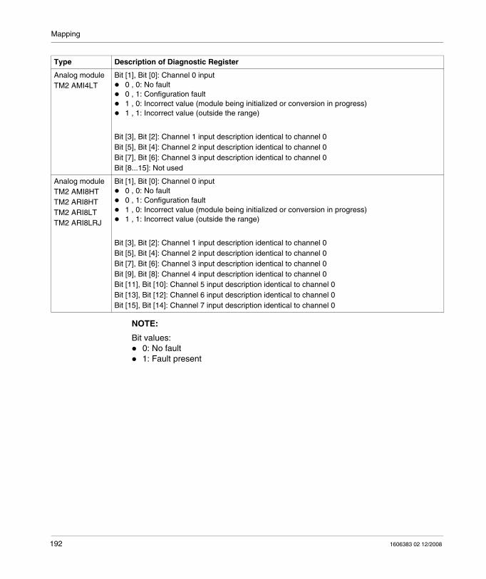
Mapping
NOTE:
Bit values:0: No fault1: Fault present
Analog moduleTM2 AMI4LT
Bit [1], Bit [0]: Channel 0 input0 , 0: No fault0 , 1: Configuration fault1 , 0: Incorrect value (module being initialized or conversion in progress)1 , 1: Incorrect value (outside the range)
Bit [3], Bit [2]: Channel 1 input description identical to channel 0Bit [5], Bit [4]: Channel 2 input description identical to channel 0Bit [7], Bit [6]: Channel 3 input description identical to channel 0Bit [8...15]: Not used
Analog moduleTM2 AMI8HTTM2 ARI8HTTM2 ARI8LTTM2 ARI8LRJ
Bit [1], Bit [0]: Channel 0 input0 , 0: No fault0 , 1: Configuration fault1 , 0: Incorrect value (module being initialized or conversion in progress)1 , 1: Incorrect value (outside the range)
Bit [3], Bit [2]: Channel 1 input description identical to channel 0Bit [5], Bit [4]: Channel 2 input description identical to channel 0Bit [7], Bit [6]: Channel 3 input description identical to channel 0Bit [9], Bit [8]: Channel 4 input description identical to channel 0Bit [11], Bit [10]: Channel 5 input description identical to channel 0Bit [13], Bit [12]: Channel 6 input description identical to channel 0Bit [15], Bit [14]: Channel 7 input description identical to channel 0
Type Description of Diagnostic Register
192 1606383 02 12/2008

Mapping
Island Management Registers
Management of Island Behavior
The OTB module management registers can be read in zones 1000...1099.
Registers Function
1000 Indicates the source of configuration parameters:0: use default values1: use saved values2: Using current unsaved values
1001 Indicates the number of backups performed. It is set to zero when default settings are restored.
1002 Save parameters command. When a value different to the current value is written to this register, the module saves the parameters and the configuration of expansion modules.
1003 Restore parameters command. When a value different to the current value is written to this register, the module restores the most recent saved parameters. The restoration will take place only if the cur-rent expansion configuration is the same as the last expansion configuration saved (if the expansion configuration allows this).
1004 Restore default parameters command. When a value different to the current value is written to this register, the module restores the default factory settings.During the restore the client parameters are lost.
1005 Reset expansion bus. This function is used to update expansion module I/O parameters:0: Setting it to zero re-activates an expansion bus reset, if the expansion bus parameters are consistent. 1: setting it to 1 initiates an expansion bus Reset. New I/O parameters written to expansion modules by the application
All outputs are set to zero when the bus is Reset.See the WARNING message below this table
1006 Network monitoring:0: default value, no monitoringx: monitoring time in ms.
1007 Bit [0]: This bit is used to relaunch network monitoring after a monitoring fault:0: Monitoring active1: Monitoring fault
Bit [1]: This bit s used to reset the default counter to zero (register 1009):1: Default counter reset to zero
1008 Bit [0]: LSB/MSB order:0: The registers concerned by the 32-bit format are in MSW / LSW format (default value)1: the registers concerned by the 32 bit format are in LSW/MSW format
Bit [1]: Fault acknowledgement mode options:0: Automatic fault acknowledgement (register 1007 automatically reset to zero)1: Manual fault acknowledgement (user must reset register 1007 to zero)
1009 Default counter
1010...1099 Reserved registers
1606383 02 12/2008 193
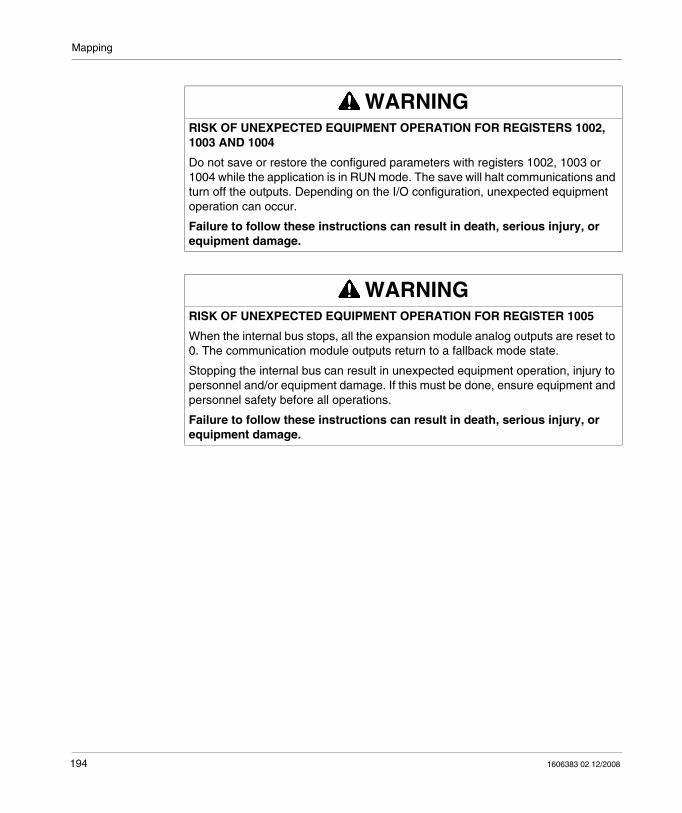
Mapping
WARNINGRISK OF UNEXPECTED EQUIPMENT OPERATION FOR REGISTERS 1002, 1003 AND 1004
Do not save or restore the configured parameters with registers 1002, 1003 or 1004 while the application is in RUN mode. The save will halt communications and turn off the outputs. Depending on the I/O configuration, unexpected equipment operation can occur.
Failure to follow these instructions can result in death, serious injury, or equipment damage.
WARNINGRISK OF UNEXPECTED EQUIPMENT OPERATION FOR REGISTER 1005
When the internal bus stops, all the expansion module analog outputs are reset to 0. The communication module outputs return to a fallback mode state.
Stopping the internal bus can result in unexpected equipment operation, injury to personnel and/or equipment damage. If this must be done, ensure equipment and personnel safety before all operations.
Failure to follow these instructions can result in death, serious injury, or equipment damage.
194 1606383 02 12/2008

Mapping
Customized Zone Registers
Definition Zone 1200...1299
The register zone to be customized is as follows:
Definition Zone 1300...1399
The register zone to be customized is as follows:
Customized Zone 2000...2099
The customized register zone which is accessible in read only is as follows:
Customized Zone 2100...2199
The customized register zone which is accessible in read/write is as follows:
Registers Function
1200...1299 Customization of the register zone accessible in read only
Registers Function
1300...1399 Customization of the register zone accessible in read/write
Registers Function
2000...2099 Read access to the customized zone of registers 1200...1299
Registers Function
2100...2199 Read/write access to the customized zone of registers 1300...1399
1606383 02 12/2008 195
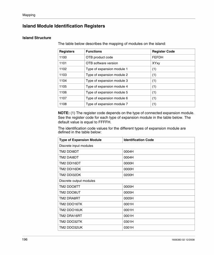
Mapping
Island Module Identification Registers
Island Structure
The table below describes the mapping of modules on the island:
NOTE: (1) The register code depends on the type of connected expansion module. See the register code for each type of expansion module in the table below. The default value is equal to FFFFH.
The identification code values for the different types of expansion module are defined in the table below:
Registers Functions Register Code
1100 OTB product code FEFDH
1101 OTB software version XYxy
1102 Type of expansion module 1 (1)
1103 Type of expansion module 2 (1)
1104 Type of expansion module 3 (1)
1105 Type of expansion module 4 (1)
1106 Type of expansion module 5 (1)
1107 Type of expansion module 6 (1)
1108 Type of expansion module 7 (1)
Type of Expansion Module Identification Code
Discrete input modules
TM2 DDI8DT 0004H
TM2 DAI8DT 0004H
TM2 DDI16DT 0000H
TM2 DDI16DK 0000H
TM2 DDI32DK 0200H
Discrete output modules
TM2 DDO8TT 0005H
TM2 DDO8UT 0005H
TM2 DRA8RT 0005H
TM2 DDO16TK 0001H
TM2 DDO16UK 0001H
TM2 DRA16RT 0001H
TM2 DDO32TK 0301H
TM2 DDO32UK 0301H
196 1606383 02 12/2008
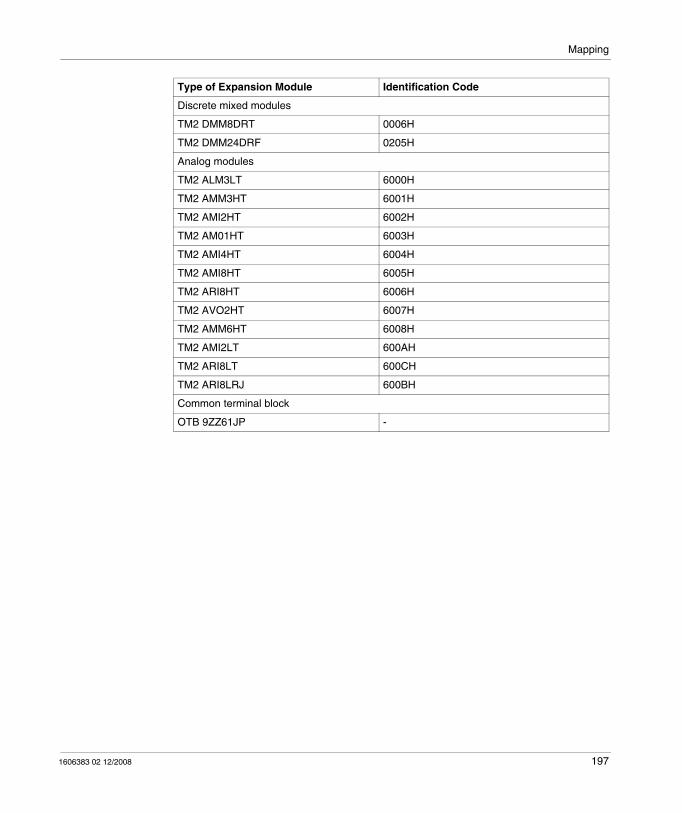
Mapping
Discrete mixed modules
TM2 DMM8DRT 0006H
TM2 DMM24DRF 0205H
Analog modules
TM2 ALM3LT 6000H
TM2 AMM3HT 6001H
TM2 AMI2HT 6002H
TM2 AM01HT 6003H
TM2 AMI4HT 6004H
TM2 AMI8HT 6005H
TM2 ARI8HT 6006H
TM2 AVO2HT 6007H
TM2 AMM6HT 6008H
TM2 AMI2LT 600AH
TM2 ARI8LT 600CH
TM2 ARI8LRJ 600BH
Common terminal block
OTB 9ZZ61JP -
Type of Expansion Module Identification Code
1606383 02 12/2008 197

Mapping
198 1606383 02 12/2008

1606383 02 12/2008
Appendices
1606383 02 12/2008 199

200 1606383 02 12/2008
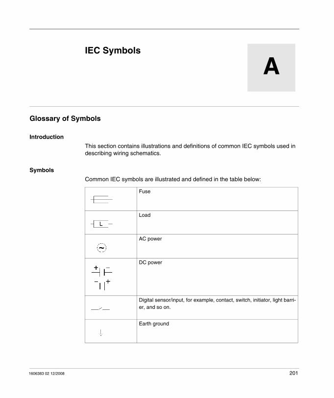
1606383 02 12/2008
A
IEC Symbols
1606383 02 12/2008
IEC Symbols
Glossary of Symbols
Introduction
This section contains illustrations and definitions of common IEC symbols used in describing wiring schematics.
Symbols
Common IEC symbols are illustrated and defined in the table below:
Fuse
Load
AC power
DC power
Digital sensor/input, for example, contact, switch, initiator, light barri-er, and so on.
Earth ground
201
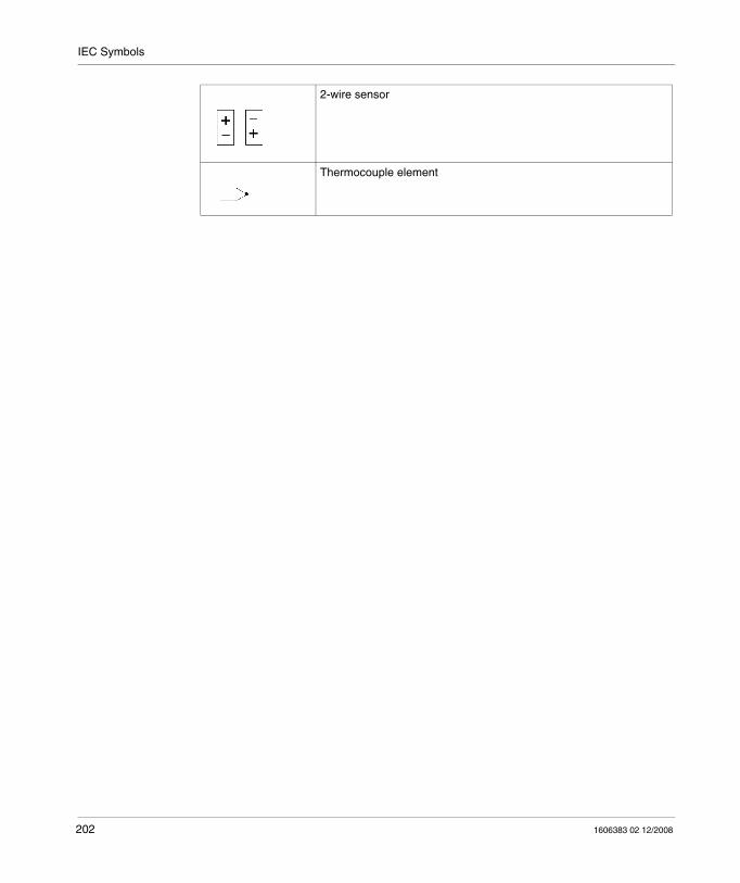
IEC Symbols
2-wire sensor
Thermocouple element
202 1606383 02 12/2008

Glossary
1606383 02 12/2008
Glossary
AAnalog Input
A module containing circuits that enable analog DC (direct current) input signals to be converted into digital values that can be handled by the processor. This implies that the analog inputs are generally direct values — in other words: a value in the data table is a direct reflection of the analog signal value.
Analog outputA module containing circuits that transmit a DC (direct current) analog signal proportional to a digital input to the processor module. This implies that the analog outputs are generally direct values — in other words: a value in the data table directly governs the analog signal value.
CCRC
Cyclic redundancy check. The messages that use this error finding mechanism have a CRC field that is calculated by the sender according to the content of the message. The receiving nodes recalculate the CRC field. Any difference between the two codes indicates a difference between the message sent and that received.
1606383 02 12/2008 203

Glossary
DDigital input/output
Another expression used is discrete input/output. Designates an input or output with a connection by individual circuit to the module corresponding directly to a data table bit or word storing the value of the signal in this I/O circuit. A digital I/O allows the control logic discrete access to the I/O values.
DIN"Deutsch Industrie Norm". German standards organization that defines dimensional and engineering standards. These standards are currently recognized worldwide.
EEIA
Electronic Industries Association. Organization that draws up data and electrical/electronic communication standards.
EMCElectro-Magnetic Compatibility. Devices that comply with EMC requirements are capable of error-free operation within the specified electro-magnetic limits of the system.
FFallback mode
A secure mode to which any Advantys I/O module can revert should the communication connection fail.
Fallback valueThe value adopted by a device when it enters the fallback state. Generally, the fallback value is either configured, or is the device's last stored value.
204 1606383 02 12/2008

Glossary
Function codeA function code is a series of instructions ordering one or more slave devices, located at one or more specified addresses, to perform a type of action, for example to read a set of data registers and to respond by writing the content of the set in question.
IIEC
International Electrotechnical Commission. Commission officially founded in 1906 and devoted to the advancement of theory and practice in the following sciences: electrical engineering, electronic engineering, information technology and computer engineering. The IEC1131 standard covers industrial automation equipment.
IEC 1 type inputType 1 digital inputs support sensor signals from mechanical switching devices such as relay contacts and push-buttons operating under normal climatic conditions.
Input filteringThe period during which a sensor must keep its signal activated/deactivated before the input module detects a change of state.
LLSB
Least Significant Byte. The part of a number, an address or a field that is written as the value furthest to the right in conventional hexadecimal or binary notation.
MModbus
Modbus is an application layer messaging protocol. Modbus enables client and server communication between devices connected via different types of bus or network. Modbus offers a large number of services specified by function codes.
1606383 02 12/2008 205

Glossary
MSBMost Significant Byte. The part of a number, an address or a field that is written as the value furthest to the left in conventional hexadecimal or binary notation.
NNEMA
National Electrical Manufacturers Association.
NO contactNormally open contact. Also called make contacts. A pair of contact relays that is open when the relay coil is low and closed when it is energized.
PPositive logic (source)
Designates an output which, when powered up, receives DC current from its load.
RRMS
Root Mean Square. The rms value of an alternating current, corresponding to the DC value which produces the same thermal effect. The RMS value is calculated by taking the square root of the mean of the squares of the instantaneous amplitude of a given full cycle. For a sinusoidal wave, the rms value corresponds to 0.707 of the peak value.
TThermocouple
A TC (thermocouple) consists of a bi-metal temperature transducer that gives a temperature value by measuring the difference in potential caused by the joining of two different metals, at different temperatures.
206 1606383 02 12/2008

Index
1606383 02 12/2008
CBA
IndexAAnalog I/O modules
characteristics, 16Mounting positions, 30
BBaud rate
selection, 77
CCabinet assembly precautions
Network interface modules, 31Characteristics
analog I/O modules, 16discrete I/O modules, 15Network interface module, 15
Communicationfieldbus, 75
Communication moduleposition of mounting holes, 27
Configurationhardware, 18
Create an island, 156
DData exchange, 171, 171Diagnostics
LEDs, 171, 171
1606383 02 12/2008
Digital I/O modulesMounting positions, 30
DimensionsNetwork interface module, 26
DIN rail15 mm AM1 DE200 rail, 40
Discrete I/ORemote Fast Counters, 98Remote Pulse Generators, 98Remote Very Fast Counters, 98
Discrete I/O modulescharacteristics, 15
EEMC Compatibility, 57Expansion module
Disassembly of a network interface mod-ule, 35
Expansion module Assembly of an expansion module, 32
FFast counter
RFC, 21Field bus interface
Pin assignment, 71Field bus or network connection, 60
207
Index
Fieldbusaddress, 74address, specification, 74speed, 76speed, specification, 76
Fieldbus masterLED, 171
FunctionRPWM, 120
II/O island
Line terminator, 23Overview, 23
Identification objects, 68IEC symbols, 201Installation on a DIN rail, 38Installation preparation, 28Island
address, 74node address, 75speed, 76
islandstatus, 170
LLEDs
COM, 171ERR, 171I0, I11, 171overview, 170PWR, 171Q0, Q7, 171
Line terminator, 23
MMaximum Hardware Configuration, 18Modbus, 66
Field bus interface, 71Modbus function codes, 67Modbus network, 70Modbus protocol, 66
208
ModuleInstallation on a DIN rail, 38Overview, 46Physical description, 47Removal of a DIN rail, 39
NNetwork considerations, 22Network interface module
Assembly of an expansion module, 32characteristics, 15Dimensions, 26Disassembly of an expansion module, 35operating range, 51output delay, 53Power connection, 55Power supply specifications, 56Removing the terminal block, 36Specific functions, 21Wiring diagram, 54
Network interface module with built-in I/O, 14Network interface modules
Cabinet assembly precautions, 31Mounting positions, 30
Nodeaddress, specification, 74speed, specification, 76
Node addressconfiguration, 75
OOperating range
network interface module, 51OTB 1S0DM9LP
LEDs, 170OTB 1S0DM9LP
Physical characteristics, 70OTB interface module
node address, 74speed, 76
Output delaynetwork interface module, 53
1606383 02 12/2008

Index
Overviewmodule, 14Module, 46
PPhysical description
Module, 47Position of mounting holes
communication module, 27Power connection
Network interface module, 55Power supply
Specifications, 56Pulse generation, 116Pulse generator
RPLS, 21Pulse generator with width modulation
RPWM, 21
RRead before starting, 28Remote Fast Counter (RFC), 99Remote Fast Counters
Discrete I/O, 98Remote Pulse Generators
Discrete I/O, 98Remote pulse width modulator, 120Remote Very Fast Counters
Discrete I/O, 98Removal
Terminal, 36RFC, 99RPLS, 116RPWM, 120RVFC, 103
SSpecific functions, 21Specifications
Power supply, 56Speed
configuration, 76, 76
1606383 02 12/2008
Starting, 28Symbols, 201
TThumbwheel, 74, 76
configuring the speed, 76node address, 75
VVery fast counter
RVFC, 21Very Fast Counter (RVFC), 103
WWiring diagram
Network interface module, 54
209

Index
210 1606383 02 12/2008