Embed Size (px)
Citation preview
REMOTE SENSING AND IMAGING
IN A RECONFIGURABLE COMPUTING ENVIRONMENT
By
VIKAS AGGARWAL
A THESIS PRESENTED TO THE GRADUATE SCHOOL OF THE UNIVERSITY OF FLORIDA IN PARTIAL FULFILLMENT
OF THE REQUIREMENTS FOR THE DEGREE OF MASTER OF SCIENCE
UNIVERSITY OF FLORIDA
2005

This document is dedicated to my parents and my sister.
ACKNOWLEDGMENTS
I would first like to thank the all mighty for giving me an opportunity to come this
far in life. I also wish to thank the department of ECE at UF, all the professors for their
words of wisdom, Dr. Alan George and Dr. Kenneth Slatton for their infinite support,
guidance and encouraging words, and all the members of the High-performance
Computing and Simulation Lab and Adaptive Signal Processing Lab for their technical
support and friendship. I also take this opportunity to thank my parents for their nurture
and support, and my sister for always encouraging me whenever I was down. I hope I
can fulfill all their expectations in life.
iii
TABLE OF CONTENTS page
ACKNOWLEDGMENTS ................................................................................................. iii
LIST OF TABLES............................................................................................................. vi
LIST OF FIGURES .......................................................................................................... vii
ABSTRACT....................................................................................................................... ix
CHAPTER
1 INTRODUCTION ........................................................................................................1
2 BACKGROUND AND RELATED RESEARCH .......................................................6
2.1 Reconfigurable Computing.....................................................................................7 2.1.1 The Era of Programmable Hardware Devices..............................................7 2.1.2 The Enabling Technology for RC: FPGAs ..................................................9
2.2 Remote-Sensing Test Application: Data Fusion...................................................13 2.2.1 Data Acquisition Process............................................................................14 2.2.2 Data Fusion: Multiscale Kalman Filter and Smoother ...............................16
2.3 Related Research ..................................................................................................20
3 FEASIBILITY ANALYSIS AND SYSTEM ARCHITECTURE .............................24
3.1 Issues and Trade-offs............................................................................................24 3.2 Fixed-point vs. Floating-point arithmetic .............................................................26 3.3 One-dimensional Time-tracking Kalman Filter Design .......................................29 3.4 Full System Architecture ......................................................................................31
4 MULTISCALE FILTER DESIGN AND RESULTS.................................................34
4.1 Experimental Setup...............................................................................................34 4.2 Design Architecture #1 .........................................................................................36 4.2 Design Architecture #2 .........................................................................................41 4.3 Design Architecture #3 .........................................................................................44 4.4 Performance Projection on Other Systems ...........................................................48
4.4.1 Nallatech’s BenNUEY Motherboard (with BenBLUE-II daughter card) ..49 4.4.2 Honeywell Reconfigurable Space Computer (HRSC) ...............................50
iv
5 CONCLUSIONS AND FUTURE WORK.................................................................52
LIST OF REFERENCES...................................................................................................56
BIOGRAPHICAL SKETCH .............................................................................................60
v
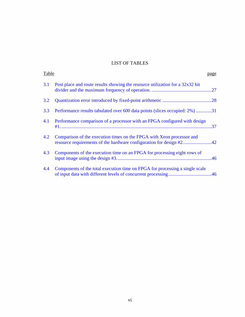
LIST OF TABLES
Table page 3.1 Post place and route results showing the resource utilization for a 32x32 bit
divider and the maximum frequency of operation. ..................................................27
3.2 Quantization error introduced by fixed-point arithmetic .........................................28
3.3 Performance results tabulated over 600 data points (slices occupied: 2%) .............31
4.1 Performance comparison of a processor with an FPGA configured with design #1. .............................................................................................................................37
4.2 Comparison of the execution times on the FPGA with Xeon processor and resource requirements of the hardware configuration for design #2........................42
4.3 Components of the execution time on an FPGA for processing eight rows of input image using the design #3. ..............................................................................46
4.4 Components of the total execution time on FPGA for processing a single scale of input data with different levels of concurrent processing....................................46
vi
LIST OF FIGURES
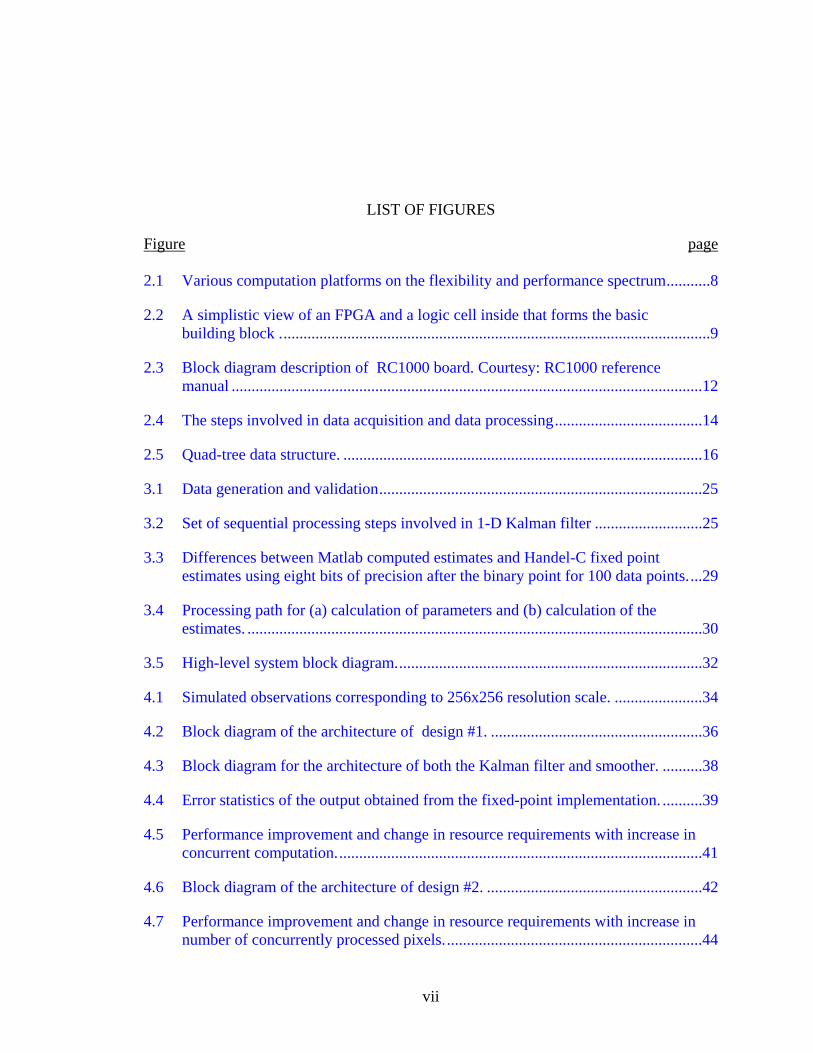
Figure page 2.1 Various computation platforms on the flexibility and performance spectrum...........8
2.2 A simplistic view of an FPGA and a logic cell inside that forms the basic building block ............................................................................................................9
2.3 Block diagram description of RC1000 board. Courtesy: RC1000 reference manual ......................................................................................................................12
2.4 The steps involved in data acquisition and data processing.....................................14
2.5 Quad-tree data structure. ..........................................................................................16
3.1 Data generation and validation.................................................................................25
3.2 Set of sequential processing steps involved in 1-D Kalman filter ...........................25
3.3 Differences between Matlab computed estimates and Handel-C fixed point estimates using eight bits of precision after the binary point for 100 data points....29
3.4 Processing path for (a) calculation of parameters and (b) calculation of the estimates. ..................................................................................................................30
3.5 High-level system block diagram.............................................................................32
4.1 Simulated observations corresponding to 256x256 resolution scale. ......................34
4.2 Block diagram of the architecture of design #1. .....................................................36
4.3 Block diagram for the architecture of both the Kalman filter and smoother. ..........38
4.4 Error statistics of the output obtained from the fixed-point implementation. ..........39
4.5 Performance improvement and change in resource requirements with increase in concurrent computation............................................................................................41
4.6 Block diagram of the architecture of design #2. ......................................................42
4.7 Performance improvement and change in resource requirements with increase in number of concurrently processed pixels.................................................................44
vii

4.8 Block diagram of the architecture of the design #3. ...............................................45
4.9 Improvement in the performance with increase in concurrent computations. .........47
4.10 Error statistics for the outputs obtained after single scale of filtering......................48
4.11 Block diagram for the hardware architecture of the Nallatech’s BenNUEY board with a BenBLUE-II extension card..........................................................................49
4.12 Block diagram of the hardware architecture of HRSC board ..................................50
viii
Abstract of Thesis Presented to the Graduate School
of the University of Florida in Partial Fulfillment of the Requirements for the Degree of Master of Science
REMOTE SENSING AND IMAGING IN A
RECONFIGURABLE COMPUTING ENVIRONMENT
By
Vikas Aggarwal
December 2005
Chair: Kenneth C. Slatton Cochair: Alan D. George Major Department: Electrical and Computer Engineering
In recent years, there has been a significant improvement in the sensors employed
for data collection. This has further pushed the envelope of the amount of data involved,
rendering the conventional techniques of data collection, dissemination and ground-based
processing impractical in several situations. The possibility of on-board processing has
opened new doors for real-time applications and reduced the demands on the bandwidth
of the downlink. Reconfigurable computing, a new star in the field of high-performance
computing, could be employed as the enabling technology for such systems where
conventional computing resources are constrained by many factors as described later.
This work explores the possibility of deploying reconfigurable systems in remote sensing
applications. As a case study, a data fusion application, which combines the information
obtained from multiple sensors of different resolution, is used to perform feasibility
analysis. The conclusions drawn from different design architectures for the test
ix

application are used to identify the limitations of current systems and propose future
systems enabled with RC resources.
x
CHAPTER 1 INTRODUCTION
Recent advances in sensor technology, such as increased resolution, frame rate, and
number of channels, have resulted in a tremendous increase in the amount of data
available for imaging applications, such as airborne and space-based remote sensing of
the Earth, biomedical imaging, and computer vision. Raw data collected from the sensor
must usually undergo significant processing before it can be properly interpreted. The
need to maximize processing throughput, especially on embedded platforms, has in turn
driven the need for new processing modalities. Today’s data acquisition and
dissemination systems need to perform more processing than the previous systems to
support real-time applications and reduce the bandwidth demands on the downlink.
Though cluster-based computing resources are the most widely used platform on ground
stations, several factors, like space, cost and power make them impractical for on-board
processing. FPGA-based reconfigurable systems are emerging as low-cost solutions
which offer enormous computation potential in both the cluster-based systems and
embedded systems arena.
Remote sensing systems are employed in many different forms, covering the gamut
from compact, power- and weight-limited satellite and airborne systems to much larger
ground-based systems. The enormous number of sensors involved in the data collection
process places heavy demands on the I/O capabilities of the system. The solution to the
problem could be approached from two directions: first, performing data compression on-
board before transmitting data; or second, performing some onboard computation and
1
2
transmitting the processed data. The target computation system must be capable of
processing multiple data streams in parallel at a high rate to support real-time
applications which further increases the complexity of the problem. The nature of the
problem demands that the processing system should not only be capable of high
performance but also be able to deliver excellent performance per unit cost (where the
cost includes several factors such as power, space and system price).
There have been a plethora of publications which have demonstrated success in
porting several remote sensing and image processing applications to FPGA-based
platforms [1-5]. Some researchers have also created high-level algorithm development
environments that expedite the porting and streamlining of such application code [6-8].
But, understanding the special needs of this class of applications and analysis of existing
platforms to determine their viability as future computation engines for remote sensing
systems warrants further research and examination. Identifying some missing
components in current platforms that are essential for such systems is the focus of this
work. A remote sensing application is used to illustrate the process. In this work, a data
fusion application has been chosen as representative of the class of remote sensing
applications, for the reason that it incorporates a wide variety of features that stress
different aspects of the target computation system.
The recent interest in sensor research has lead to a multitude of sensors in the
market, which differ drastically in their phenomenology, accuracy, resolution and
quantity of data. Traditionally, Interferometric Synthetic Aperture Radar (InSAR) has
been employed for mapping extended areas of terrain with moderate resolution. Airborne
Laser Swath Mapping (ALSM) has been increasingly employed to map local elevations
3
at high resolution over smaller regions. A multiscale estimation framework can then be
employed to fuse the data obtained from such different sensors having different
resolutions to produce improved estimates over large coverage areas while maintaining
high resolution locally. The nature of the processing involved imposes enormous
computation burden on the system. Hence, the target system should be equipped with
enormous computation potential.
Since their inception, early processing systems have fallen into two separate camps.
The first camp saw a need to accommodate wide varieties of applications with multiple
processes running concurrently on the same system, and therefore chose General-Purpose
Processors (GPP) to serve their needs. The other camp preferred to improve on the speed
of the application and chose to leverage the performance advantages of the Application-
Specific Integrated Circuits (ASICs). Over a period of time, these two camps strayed
further apart in terms of processing abilities, flexibility and costs involved.
Meanwhile, due to the technological advancements over the past decade,
Reconfigurable Computing (RC) has garnered a great deal of attention from both the
academic community and industry. Reconfigurable systems have tried to fuse the merits
of both the camps and have proven to be a promising alternative. RC has demonstrated
improved performance in speed on the order of 10 to 100 in comparison to GPPs for
certain application domains such as image and signal processing [2, 4, 5, 9]. An even
more remarkable aspect of this relatively new programming paradigm is that the
performance improvements are obtained at less than two thirds of the cost of
conventional processors. FPGA-enabled reconfigurable processing platforms have even
outperformed the ASICs in market domains including signal processing and cryptography
4
where ASICs and DSPs have been the dominant modalities for decades. The past decade
has seen a mountainous growth in RC technology, but it is still in its infancy stage. The
development tools, target system architectures and even processes for porting the
applications need to mature before they can make meaningful accomplishments.
However, RC-based designs have already shown performance speedups in
application domains such as image processing which require similar processing patterns
to many remote-sensing applications. Conventional processor-based resources cannot be
employed in such applications because of their inherent limitations of size, power and
weight, which RC-based systems can overcome. The structure of imaging algorithms
lends itself to a high degree of parallelism that can be exploited in hardware by the
FPGAs. The computations are often data-parallel, require little control, and contain large
data sets (effectively infinite streams), and raw sensor data elements that do not have
large bit widths, making them amenable to RC. However, this class of applications has
three characteristics which make them challenging. First, they involve many arithmetic
operations (e.g. multiply-accumulates and trigonometric functions) on real and/or
complex data. Second, they require significant memory support, not just in the capacity
of memory but also in the bandwidth that can be supported. Third, the scale of
computation is large, requiring (possibly) hundreds of parallel operations per second and
high-bandwidth interconnections to meet real-time constraints. These challenges must be
addressed if RC systems are to significantly impact future remote-sensing systems. This
work explores the possibility of deploying reconfigurable systems in remote-sensing
applications using the chosen test case for feasibility analysis. The conclusions drawn
from different design architectures for the test applications are used to identify the
5
limitations of the current systems and propose solutions to enable future systems with RC
resources.
The structure of the remaining document is as follows. Chapter 2 presents a brief
background on reconfigurable computing using FPGAs as the enabling technologies and
data fusion using multiscale Kalman filters/smoothers. It also presents a discussion on
the related research in the field of reconfigurable computing as applied to remote sensing
and similar application domains. Chapter 3 presents some tests performed for initial
study and feasibility analysis. The experiments are based on designs of the 1-D Kalman
filter, which forms the heart of the calculations involved in the data fusion application.
Chapter 4 presents a sequence of revisions to 2-D filter designs developed to solve the
problem along with the associated methodologies. Each of these designs builds on the
limitations identified in the previous design and proposes a better solution under the
given system constraints. Their performance is compared with a baseline C code running
on a Xeon processor. Several graphs and tables that are derived from the results are also
presented. The final architecture in the chapter emulates the performance of an ideal
system due to which it outperforms the processor-based solution by achieving over an
order of magnitude speedup. Chapter 5 summarizes the research and the findings of this
work. It draws conclusions based on the results and observations presented in the
previous chapters. It also gives some future directions for work beyond this thesis.

CHAPTER 2 BACKGROUND AND RELATED RESEARCH
This work involves an interdisciplinary study of remote-sensing applications and a
new paradigm in the field of high-performance computing: Reconfigurable Computing.
The fast development times with reconfigurable devices, their density, advanced features
such as optimized compact hardwire cores, programmable interconnections, memory
arrays, and communication interfaces have made them a very attractive option for both
terrestrial and space-/air-borne applications. There are multiple advantages of equipping
future systems with reconfigurable computation engines. First, they help in overcoming
the limited bandwidth problem on the downlink. Second, they create a possibility of
providing several real-time applications on-board. Third, they can also be used for
feedback mechanisms to change data collection strategy in response to the quality of the
received data or for changing instrumentation planning policy.
This thesis aims at designing different architectures for a test application to analyze
various features of the existing platforms and suggest necessary improvements. The
hardware designs for the FPGA are implemented using the Handel-C language (with DK-
3 as its integrated development environment) to expedite the process as compared to the
conventional HDL design flow. This chapter provides a comprehensive discussion on
different aspects of reconfigurable computing with a brief description of the application.
To summarize the existing research, a brief review of the relevant prior work in this field
and other related fields is also presented in this chapter.
6
7
2.1 Reconfigurable Computing
This section presents some history on the germination, progress and recent
explosion of this relatively new computing paradigm. This section also describes the rise
in usage of programmable logic devices in general with time and concludes with a
detailed discussion on the enabling technology for RC: FPGAs.
2.1.1 The Era of Programmable Hardware Devices
From the infancy of Application-Specific Integrated Circuits (ASICs) the designers
could foresee a need for chips with specialized hardware that would provide enormous
computational potential. The state of the art of IC fabrication technology limited the
amount of logic that could be packed into a single chip. During the 1980s and 90s the
fabrication technology matured and saw drastic improvements in many fabrication
processes, and the era of VLSI began. The high development and fabrication costs
started dropping as the 90s saw an explosion in the demands of such products.
The 1980s and 90s also saw birth of the killer “microprocessors” [10] which started
capturing a big portion of the market. The faster time to market for the products
motivated many to forgo ASIC and adopt general-purpose processors (GPP) or special-
purpose processors such as digital signal processors (DSPs). While this approach
provided a great deal of success in several application domains with relative simplicity, it
was never able to match the performance of the specialized hardware in the high-
performance computing (HPC) community. Real-time systems and other HPC systems
with heavy computational demands still had to revert to ASIC implementations. To
overcome the limitation of high non-recurring engineering (NRE) costs and long
development times, an alternative methodology was developed: Programmable Logic
Devices (PLDs). PLDs started playing a major role in the early 90s. Since they provided
8
faster design cycles and mitigated the initial costs, they were soon adopted as inexpensive
prototyping tools to perform design exploration for ASIC-based systems. As the
technology matured, the application of PLDs expanded beyond their role as “place
holders” into essential components of the final systems [11].
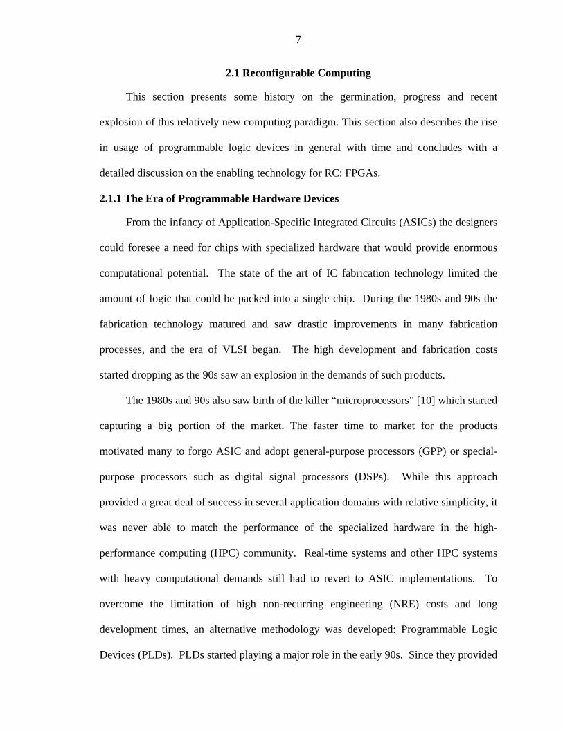
Due to their ability of being programmed in-field, developers could foresee the
PLDs playing a major role in HPC where they could offer many advantages over
conventional GPPs and ASICs. The GPP and the ASIC have existed at two extremes on
the spectrum of computational resources. The key trade-off has been that of flexibility,
where GPPs have held the lead in the market, and performance, where the ASICs have
overshadowed the former. PLDs (also known as RC engines because of their ability to be
reprogrammed) have made a strong impact in the market by providing the best of both
the worlds.
Figure 2.1. Various computation platforms on the flexibility and performance spectrum
9
2.1.2 The Enabling Technology for RC: FPGAs
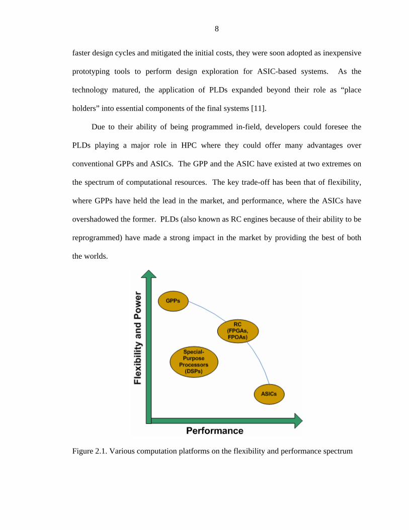
As gate density further improved, a particular family of PLDs, namely FPGAs,
became a particularly attractive option for researchers. An FPGA consists of an array of
configurable logic elements along with a fully programmable interconnect fabric capable
of providing complex routing between these logic elements [12]. Figure 2.2 presents an
oversimplified structure of an FPGA. The routing resources represented in the diagram
by horizontal and vertical wires that run between the Configurable Logic Blocks (CLBs)
consume over 75% of the area on the chip. The flexible nature of an FPGA’s architecture
provides a platform upon which applications could be mapped efficiently. The ability to
reconfigure the logic cells and the connections allows for modifying the behavior of the
system even after deployment. This feature has important implications for supporting
multiple applications, as an FPGA-based system could eliminate the need of creating a
new system each time a new application is to be ported.
I/O I/O I/O I/OI/O I/O
CLB CLB CLB I/OI/O CLB
CLB CLB CLB I/OI/O CLB
I/O CLB CLB CLB CLB I/O
CLB CLB CLB I/OI/O CLB
I/O I/O I/O I/O I/O I/O
Configurable Logic Blocks:LUT + FlipFlops
Programmable Connections
I/O Blocks: accessto externalpins
Figure 2.2. A simplistic view of an FPGA and a logic cell inside that forms the basic building block [13].
10
Modern FPGAs are embedded with a host of advanced processing blocks such as
hardware multipliers and processor cores to make them more amenable for complex
processing applications.
One of the several advantages that FPGAs offer over conventional processors is
that they are massive computing machines that lend themselves well to applications with
inherent fine-grain parallelism. Because a “farm” of CLBs can operate completely
independently, a large number of operations can take place on-chip simultaneously unlike
in most other computing devices. The ability of concurrent computation and support for
high memory bandwidth offered by internal RAMs in FPGAs offers them an edge over
DSPs for several signal processing applications. Highly pipelined designs help further in
overlapping and hiding latencies at various processing steps. The execution time for the
control system software is difficult to predict on modern processors because of cache,
virtual memory, pipelining and several other issues which make the worst-case
performance significantly different from the average case. In contrast, the execution time
on the FPGAs is deterministic in nature, which is an important factor for time-critical
applications.
Although FPGAs provide a powerful platform for efficiently creating highly
optimized hardware configurations of applications, the process of configuration
generation can be quite labor-intensive. Hence, researchers have been looking for
alternative ways of porting applications with relative ease. Several graphical tools and
higher-level programming tools are being developed by vendors that speed up the design
cycle of porting an application on the FPGA. This thesis makes use of one such high-
level programming tool called Handel-C (started as a project at Oxford University and
11
later developed into a commercial tool by Celoxica Inc.) [8] to enable fast prototyping
and architectural analysis. Handel-C provides an extension and somewhat of a superset
of standard ANSI C including additional constructs for communication channels and
parallelization pragmas while simultaneously removing support for many ANSI C
standard libraries and other functionality such as recursion and compound assignments.
DK the development environment that supports Handel-C, provides floating-point and
fixed-point libraries. The compiler can produce synthesizable VHDL or an EDIF netlist
and supports functional simulation. Handel-C and its corresponding development
environment have been used previously in numerous other projects including image
processing algorithms [14] and other HPC benchmarks [2].
The most common way in which RC-based systems exist today are as extensions to
conventional processors. The FPGAs are integrated with memory and other essential
components on a single board which then attaches to the host processor through some
interconnect such as a Peripheral Component Interconnect (PCI) bus.
This work makes use of an RC1000 board, a PCI-based board developed by
Celoxica Inc. equipped with a VirtexE 2000 FPGA. Hardware configurations for the
board can be generated using the DK development environment or following the more
conventional design path of VHDL. Figure 2.3 shows a block diagram of the RC1000
board. The card consists of 8MB of memory that is organized into four independently
accessible banks of 2MB each. The memory is accessible both to the FPGA and any
other device on the PCI bus. The FPGA has two clock inputs on the global clock buffer.
The first pin derives its clock from a programmable clock source or an external clock,
whereas the second pin derives its clock from the second programmable clock source or
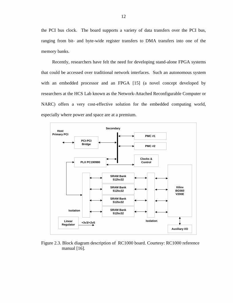
12
the PCI bus clock. The board supports a variety of data transfers over the PCI bus,
ranging from bit- and byte-wide register transfers to DMA transfers into one of the
memory banks.
Recently, researchers have felt the need for developing stand-alone FPGA systems
that could be accessed over traditional network interfaces. Such an autonomous system
with an embedded processor and an FPGA [15] (a novel concept developed by
researchers at the HCS Lab known as the Network-Attached Reconfigurable Computer or
NARC) offers a very cost-effective solution for the embedded computing world,
especially where power and space are at a premium.
SRAM Bank512kx32
SRAM Bank512kx32
SRAM Bank512kx32
SRAM Bank512kx32
PCI-PCIBridge
PLX PC190980
PMC #1
PMC #2
Clocks &Control
Xilinx BG560V200E
Linear Regulator
Auxiliary I/O
HostPrimary PCI
Secondary
Isolation+3v3/+2v5
Isolation
Figure 2.3. Block diagram description of RC1000 board. Courtesy: RC1000 reference manual [16].
13
2.2 Remote-Sensing Test Application: Data Fusion
In the past couple of decades, there has been a tremendous amount of research in
sensor technology. This research has resulted in a rapid advancement of related
technologies and a plethora of sensors in the market that differ significantly in the quality
of data they collect. One of the most important applications that have attracted
overwhelming attention in remote sensing is that of mapping topographies and building
digital elevation maps of regions of earth using different kinds of sensors. These maps
are then employed by researchers in different disciplines for various scientific
applications (e.g. oceanography for estimation of ocean surface heights and behavior of
currents, in geodesy for estimation of earth’s gravitational equipotential, etc.).
Traditionally, satellite-based systems equipped with sensors like InSAR and
Topographic Synthetic Aperture Radar (TOPSAR) had been employed to map extended
areas of topography. But, these sensors lacked high accuracy and produced images of
moderate resolution over the region of interest. Recently, ALSM has emerged as an
important technology for remotely sensing topographies. ALSM sensor provides
extremely accurate and high resolution maps of local elevations, but operates through a
very exhaustive process which limits the coverage areas to smaller regions.
Because of the varying nature of the data produced by these sensors, researchers
have been developing algorithms that fuse information obtained at different resolutions
into a single elevation map. A multiscale estimation framework developed by Feiguth
[17] has been employed extensively over the past decade for performing efficient
statistical analysis, interpolation, and smoothing. This framework has also been adopted
to fuse ALSM and InSAR data having different resolutions to produce improved
estimates over large coverage areas while maintaining high resolution locally.
14
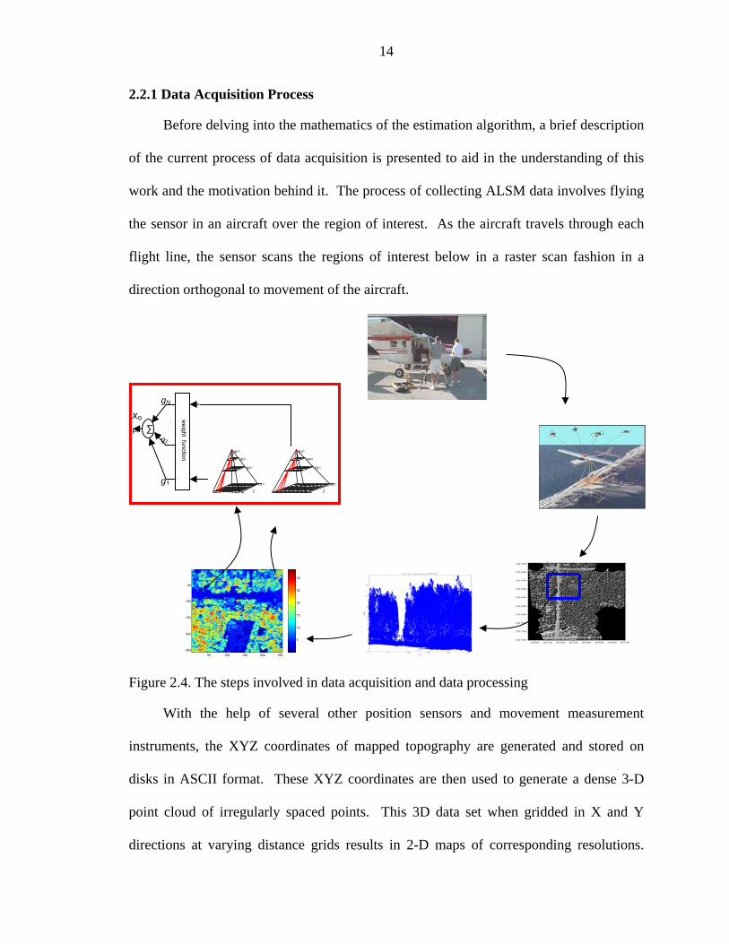
2.2.1 Data Acquisition Process
Before delving into the mathematics of the estimation algorithm, a brief description
of the current process of data acquisition is presented to aid in the understanding of this
work and the motivation behind it. The process of collecting ALSM data involves flying
the sensor in an aircraft over the region of interest. As the aircraft travels through each
flight line, the sensor scans the regions of interest below in a raster scan fashion in a
direction orthogonal to movement of the aircraft.
50 100 150 200 250
50
100
150
200
250
5
10
15
20
25
30
Figure 2.4. The steps involved in data acquisition and data processing
With the help of several other position sensors and movement measurement
instruments, the XYZ coordinates of mapped topography are generated and stored on
disks in ASCII format. These XYZ coordinates are then used to generate a dense 3-D
point cloud of irregularly spaced points. This 3D data set when gridded in X and Y
directions at varying distance grids results in 2-D maps of corresponding resolutions.
m=m=
m=
m=2
m=m=
m=
m=2
weight function
gN
g1
g2
.
. ∑ .xo
pt
15
These images are then employed in the multiscale estimation framework with the SAR
images to fuse the data sets and produce improved maps of topography. Because of the
lack of processing capabilities on aircraft, these operations cannot be performed in real-
time and hence data is stored on disk and processed offline in ground stations. Several
applications could be made possible if on-board processing facilities were made available
on the aircraft. Such a real-time system would offer several advantages over the
conventional systems. For example, it could be used to change the data collection
strategy or repeat the process over certain selected regions in response to the quality of
data obtained. RC-based platforms as described in the previous section form a perfect fit
for being deployed in such systems. Although this work closely deals with an aircraft-
based target system, the issues involved are very generic and apply to most other remote
sensing systems with some exceptions. As a result some issues might not be addressed in
this work, for example the effect of radiations which have important implications on
satellite-based systems, requiring some kind of redundancy is provided to overcome
single event upsets (SEUs), do not affect an aircraft-based system. While it is desirable
to design a complete system that could be deployed on-board an aircraft, doing so would
entail a plethora of implementations issues that divert the focus from the more interesting
aspects of this work explored through research. Hence, instead of building an end-to-end
system, this work will focus on the data fusion application employed in the entire process
(Figure 2.4) and will use it as a test case to analyze the feasibility of deploying RC-based
systems in the remote sensing arena. The following sub-section provides a description of
this data fusion algorithm.
16
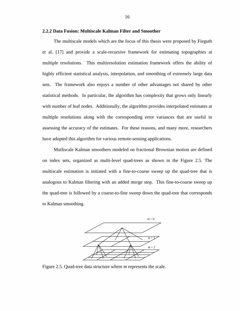
2.2.2 Data Fusion: Multiscale Kalman Filter and Smoother
The multiscale models which are the focus of this thesis were proposed by Fieguth
et al. [17] and provide a scale-recursive framework for estimating topographies at
multiple resolutions. This multiresolution estimation framework offers the ability of
highly efficient statistical analysis, interpolation, and smoothing of extremely large data
sets. The framework also enjoys a number of other advantages not shared by other
statistical methods. In particular, the algorithm has complexity that grows only linearly
with number of leaf nodes. Additionally, the algorithm provides interpolated estimates at
multiple resolutions along with the corresponding error variances that are useful in
assessing the accuracy of the estimates. For these reasons, and many more, researchers
have adopted this algorithm for various remote-sensing applications.
Mutliscale Kalman smoothers modeled on fractional Brownian motion are defined
on index sets, organized as multi-level quad-trees as shown in the Figure 2.5. The
multiscale estimation is initiated with a fine-to-coarse sweep up the quad-tree that is
analogous to Kalman filtering with an added merge step. This fine-to-coarse sweep up
the quad-tree is followed by a coarse-to-fine sweep down the quad-tree that corresponds
to Kalman smoothing.
m = 0
m = 1
m = 2
Figure 2.5. Quad-tree data structure where m represents the scale.

17
The statistical process defined on the tree is related to the observation process and has the
coarse-to-fine scale mapping defined as follows
)()()()()( swsBsxsAsx += γ (1)
)()()()( svsxsCsy += (2)
where
s represents an abstract index for representing a node on the tree
γ represents the lifting operator, γs represents the parent of s
) represents the state variable (sx
) represents the observation (LIDAR or INSAR) (sy
) represents the state transition operator (sA
) represents the stochastic detail scaling function (sB
) represents the measurement state relation (sC
) represents the white process noise (sw
) represents the white measurement noise (sv
α represents the lowering operator, nsα represents the nth child of s
q represents the order of the tree, i.e. the number of descendant a parent has
The process noise , is Gaussian with zero mean and the variance given by the
following relation
)(sw
tsttwsw ,])()([ δΙ=Ε (3)
),0(~)( ΙNsw (4)
The prior covariance at the root node is given by
),0(~)0( 00 Ρ= Nxx (5)
18
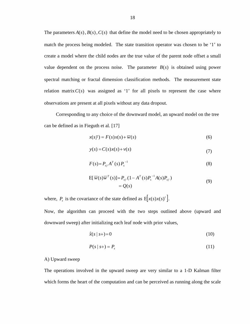
The parameters , , )C that define the model need to be chosen appropriately to
match the process being modeled. The state transition operator was chosen to be ‘1’ to
create a model where the child nodes are the true value of the parent node offset a small
value dependent on the process noise. The parameter is obtained using power
spectral matching or fractal dimension classification methods. The measurement state
relation matrix was assigned as ‘1’ for all pixels to represent the case where
observations are present at all pixels without any data dropout.
)(sA )(sB (s
)(sB
)(sC
Corresponding to any choice of the downward model, an upward model on the tree
can be defined as in Fieguth et al. [17]
)()()()( swsxsFsx +=γ (6)
)()()()( svsxsCsy += (7)
1)()( −= sT
s PsAPsF γ (8)
)())()(1()]()([ 1
sQPsAPsAPswsw ss
Ts
T
=
−=Ε −γγ (9)
where, is the covariance of the state defined as sP [ ]tsxsx )()(Ε .
Now, the algorithm can proceed with the two steps outlined above (upward and
downward sweep) after initializing each leaf node with prior values,
0)|(ˆ =+ssx (10)
sPssP =+)|( (11)
A) Upward sweep
The operations involved in the upward sweep are very similar to a 1-D Kalman filter
which forms the heart of the computation and can be perceived as running along the scale
19
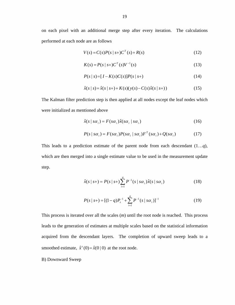
on each pixel with an additional merge step after every iteration. The calculations
performed at each node are as follows
)()()|()()( sRsCssPsCsV T ++= (12)
)()()|()( 1 sVsCssPsK T −+= (13)
)|()]()([)|( +−= ssPsCsKIssP (14)
))|(ˆ)()()(()|(ˆ)|(ˆ +−++= ssxsCsysKssxssx (15)
The Kalman filter prediction step is then applied at all nodes except the leaf nodes which
were initialized as mentioned above
)|(ˆ)()|(ˆ iiii ssxsFssx αααα = (16)
)()()|()()|( iiT
iiii sQsFssPsFssP αααααα += (17)
This leads to a prediction estimate of the parent node from each descendant (1…q),
which are then merged into a single estimate value to be used in the measurement update
step.
∑=
−+=+q
iii ssxssPssPssx
1
1 )|(ˆ)|()|()|(ˆ αα (18)
∑=
−−− +−=+q
iis ssPPqssP
1
111 )]|()1[()|( α (19)
This process is iterated over all the scales (m) until the root node is reached. This process
leads to the generation of estimates at multiple scales based on the statistical information
acquired from the descendant layers. The completion of upward sweep leads to a
smoothed estimate, at the root node. )0|0(ˆ)0(ˆ xxs =
B) Downward Sweep
20
The smoothed estimates for the remaining nodes are computed by propagating the
information back down the tree in a smoothing step.
)]|(ˆ)(ˆ)[()|()(ˆ ssxsxsJssxsx ss γγ −+= (20)
)()]|()()[()|()( sJssPsPsJssPsP Tss γγ −+= (21)
)|()()|()( 1 ssPsFssPsJ T γ−= (22)
where
) represents the smoothed estimates (ˆ sxs
)(sPs represents the corresponding error variances
It is worth mentioning here that the set of computations outlined above, despite being
closely coupled, have two independent processing paths. This fact is further exploited in
Chapters 3 and 4 where the designs for targeting the hardware are explored.
2.3 Related Research
There has been an abundance of publications over the past decade by researchers
who have tried accelerating various image processing algorithms on FPGAs. There has
also been a good deal of academic and industry effort in deploying such dual-paradigm
systems (which make use of both conventional processing resources and RC-based
resources) in space for improving on-board performance. However, only a limited
amount of work has been done in understanding the nature of processing involved in such
applications to identify their specialized demands from the target systems.
One of the earliest works on designing a Kalman filter for an FPGA was by Lee
and Salcic in 1997 [18], where they attempted to accelerate a Kalman tracking filter for
multi-target tracking radar systems. They achieved an order of magnitude improvement
with their designs that spread over six 8000-series Altera chips in comparison to previous
21
attempts in [19-22] that targeted transputers, digital signal processors, and linear arrays
for obtaining improved performance over software implementations. In an application
note from Celoxica Inc. [23], Chappel, Macarthur et al. present a system implementation
for boresighting of sensor apertures using a Kalman filter for sensor fusion. The system
utilizes a COTS-based FPGA which embeds a 32-bit softcore processor to perform the
filtering operation. Their work serves as a classical example of developing a low-cost
solution for embedded systems using FPGAs. There have also been other works [24-25]
that perform Kalman filtering using an FPGA for solving similar problems such as
implementation of a state space controller and real-time video filtering. In [25], Turney,
Reza, and Delva have astutely performed pre-computation of certain parameters to reduce
the resource requirements of the algorithm.
The floating-point calculations involved in signal processing algorithms are not
amenable to FPGA or hardware implementations in general, so researchers have resorted
to fixed-point implementations and have been exploring ways to mitigate the errors hence
induced. In [18], Lee and Salcic employ normalization of certain coefficients involved
by the process variance to maximize data accuracy with a fixed number of bits or
minimize the resource requirements for a certain level of accuracy. There has also been
plenty of work done on the algorithmic side to overcome such effects. In [26], Scharf
and Siggurdsson present a study of scaling rules and round off noise variances in a fixed
point implementation of a Kalman filter.
The 1-D Kalman filter involves heavy sequential processing steps and hence cannot
fully exploit the fine-grain parallelism available in FPGAs. The multiscale Kalman filter
by contrast involves independent operations on multiple pixels in an image and offers a
22
high degree of parallelism (DoP) that is representative of the class of image processing
algorithms. The possibility of operating on multiple pixels in parallel has motivated
many researchers to target different imaging algorithms on FPGAs. Researchers [2, 4, 5,
9] have presented several examples illustrating the performance improvements obtained
by porting imaging algorithms like 2-D Fast Fourier Transform, image classification,
filtering, 2-D convolution and edge detection on the FPGA-based platforms. Dawood,
Williams and Visser have developed a complete system [27] for performing image
compression using FPGAs on-board a satellite to reduce bandwidth demands on the
downlink. Several researchers have even developed a high-level environment [6-7] to
provide the application programmers a much easier interface for targeting FPGAs for
imaging applications. They achieve this goal by developing a parameterized library of
commonly employed kernels in signal/image processing, and these cores can then be
instantiated from a high-level environment as needed by the application.
Employing RC technology in the remote sensing arena is not a new concept and
several attempts have been made previously to take advantage of this technology. Buren,
Murray and Langley in their work [28] have developed a reconfigurable computing board
for high-performance computing in space using SRAM-based FPGAs. They have
addressed the special needs for such systems and identified some key components that
are essential to the success, such as, the use of high-speed dedicated memories for FPGAs
and high I/O bandwidth and support for periodic reloading to mitigate radiation effects
being some of them. In [3], Arribas and Macia have developed an FPGA board for a
real-time vision development system that has been tailored for the embedded
environment. Besides the academic research community, industries have also shown
23
keen interest in the field. Honeywell has developed a “Honeywell Reconfigurable Space
Computer” (HRSC) [29] board as a prototype of the RC adaptive processing cell concept
for satellite-based processing. The HRSC incorporates system-level SEU mitigation
techniques and facilitates the implementation of design-level techniques. In addition to
hardware development research, abundance of work has been done on developing
hardware configurations for various remote-sensing applications. In [1], a SAR/GMTI
range compression algorithm has been developed for an FPGA-based system. Sivilotti,
Cho et al., in their work in [30], have developed an automatic target detection application
for SAR images to meet the high bandwidth and performance requirements of the
application. Other works in [27, 31-33] discuss the issues involved in porting similar
applications such as geometric global positioning, sonar processing, etc. on the FPGAs.
This thesis aims to further the existing research in this field by developing a multiscale
estimation application for an FPGA-enabled system and exploring different architectures
to meet the system requirements.
CHAPTER 3 FEASIBILITY ANALYSIS AND SYSTEM ARCHITECTURE
This chapter presents a discussion on some of the issues involved and some initial
experiments performed for feasibility analysis. The results of these tests influenced the
choice of design parameters and architectural decisions made for the hardware designs of
the algorithm presented in the next chapter.
3.1 Issues and Trade-offs
Most signal processing algorithms executed on conventional platforms employ
double-precision, floating-point arithmetic. As pointed out earlier, such floating-point
arithmetic is not amenable to hardware implementations on FPGAs, as they have large
logic area requirements (a more detailed comparison is presented in the next subsection).
Carrying out these processing steps in fixed-point arithmetic is desirable but introduces
quantization error which if not controlled can lead to errors large enough to defeat the
purpose of hardware acceleration. Hence, there exists an important trade-off between the
number of bits used and the amount of logic area required. There are techniques that
mitigate these effects by modifying certain parts of the algorithm itself. Examples of
such techniques include normalizing of different parameters to reduce the dynamic range
of variables and using variable bit precisions for different parameters, using more bits for
more significant variables. This work makes use of fixed- and floating-point libraries
available in Celoxica’s DK package. To perform experimental analysis, the simulated
data is generated using Matlab (the values for the simulated data were chosen to closely
represent the true values of data acquired from the sensors). Hence, a procedure is
24

25
required to verify the models in the FPGA with the data generated in Matlab. Text files
are used in this work as a vehicle to carry out the task. Since Matlab produces double-
precision, floating-point data while the FPGA requires fixed-point values, extra
processing is needed to perform the conversion.
Figure 3.1. Data generation and validation
Another important issue that can become a significant hurdle arises from the nature
of the processing involved in the Kalman filtering algorithm. The Kalman filter
equations are recursive in nature and require the current iteration estimate value to begin
the next state calculation. This behavior is clearly visible from Figure 3.2 which shows
the processing steps in a time-tracking filter.
Figure 3.2. Set of sequential processing steps involved in 1-D Kalman filter
Initial prior values
Measurement update Time update
kT
kkk
Tkk
k RHPHHPK
+= −
−
)ˆ(ˆˆ −− −+= kkkkkk xHzKxx
kT
kkkk
kkk
QPP
xx
+ΦΦ=
Φ=−+
+
1
1
−−Ι= kkkk PHKP )(
.txt file containing data
Hardware
Handel-C/VHDL
Matlab simulation and
kx represents the state variable represents associated error covariance kP
kz represents the observation input represents process noise variance kQΦ represents the state transition operator represents measurement noise variance kR

26
This problem cannot be mitigated by pipelining the different stages, because of the data
dependency that exists from the last stage of the pipeline to the first stage. Although this
can be a major roadblock for 1-D tracking algorithms, the situation can be made much
better in the multiscale filtering algorithm because of the presence of an additional
dimension where the parallelism can be exploited along the scale. Multiple pixels in the
same scale can be processed in parallel as they are completely independent of each other.
The number of such parallel paths would ultimately depend on the amount of resources
required by the processing path of each pixel pipeline. Another interesting but subtle
trade-off exists between the memory requirements and the logic area requirements.
Hardware architecture of the algorithm could be made to reuse some resources on the
chip (e.g. the arithmetic operations that are instantiated could be reused, especially
modules such as multipliers and the dividers which consume excessive area) by saving
the intermediate results in the on-board SRAM. This approach decreases the logic area
demands of the algorithm, but at the cost of increased memory requirements and also the
extra clock cycles required for computing each estimate.
3.2 Fixed-point vs. Floating-point arithmetic
A study was performed to compare the resource demands posed by floating-point
operations as opposed to fixed-point and integer operations of equal bit widths. Since a
division operation is a very expensive operation in hardware, it yields more meaningful
differences and was hence chosen as the test case. IEEE single-precision format was
employed for floating-point division. A Xilinx VirtexII chip was chosen as the target
platform for the experiment to exploit the multiplier components present in the device
(and also partly due to the fact that the current version of the tool does not support

27
floating-point division on any other platform). Table 3.1 compares the resource
requirements for the different cases.
Table 3.1. Post place and route results showing the resource utilization for a 32×32 bit divider and the maximum frequency of operation.
Target Chip: VirtexII 6000
Package: ff1152
Speed Grade: -4
Integers (32 bits)
Fixed-point ( 16 bits beforeand after binary point)
IEEE single-precision floating-point (32 bits)
Slices (Total 33792) 19 (1%) 84 (1%) 487 (1%)
18-bit×18-bit Multipliers (Total 144)
3 (2%) 6 (4%) 4 (2%)
Max. frequency 63.2 MHz 50.5 MHz 97.5 MHz High costs involved in the floating-point operations are clearly visible from the table.
The high frequency obtained for the floating-point unit, which appears as an anomaly,
merely represents the efficiency of the cores used by the library in the tool. Once the cost
savings obtained by resorting to the fixed-point operations have been identified, we need
to understand the error introduced through this process. To analyze this error, multiple
designs of the 1-D filter were developed with different bit widths of fixed-point
implementations in Handel-C. Although simulation was adopted to generate the outputs,
the designs were made to closely represent hardware models such that minimal changes
could translate them into hardware configurations. The simulation outputs were
compared with Matlab’s double-precision floating results. Mean square error (MSE)
between the filter estimates and the actual expected outputs were used as a metric for
comparison as shown in Table 3.2.
28
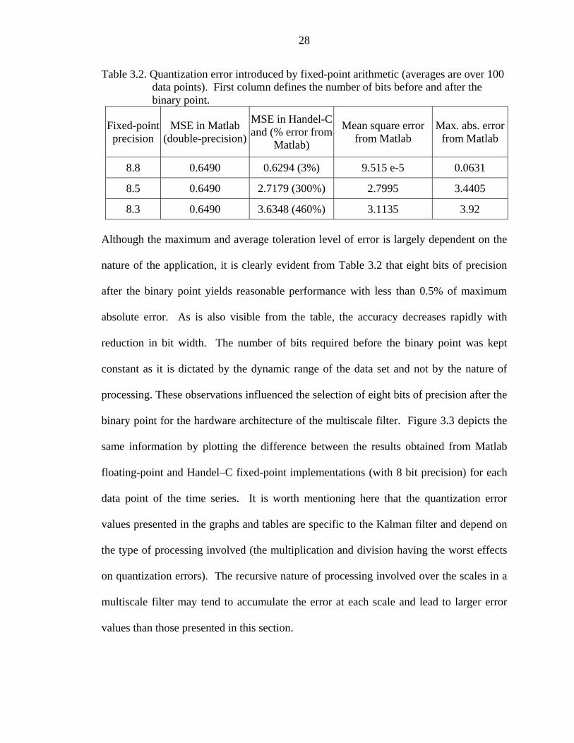
Table 3.2. Quantization error introduced by fixed-point arithmetic (averages are over 100 data points). First column defines the number of bits before and after the binary point.
Fixed-point precision
MSE in Matlab (double-precision)
MSE in Handel-Cand (% error from
Matlab)
Mean square error from Matlab
Max. abs. error from Matlab
8.8 0.6490 0.6294 (3%) 9.515 e-5 0.0631
8.5 0.6490 2.7179 (300%) 2.7995 3.4405
8.3 0.6490 3.6348 (460%) 3.1135 3.92 Although the maximum and average toleration level of error is largely dependent on the
nature of the application, it is clearly evident from Table 3.2 that eight bits of precision
after the binary point yields reasonable performance with less than 0.5% of maximum
absolute error. As is also visible from the table, the accuracy decreases rapidly with
reduction in bit width. The number of bits required before the binary point was kept
constant as it is dictated by the dynamic range of the data set and not by the nature of
processing. These observations influenced the selection of eight bits of precision after the
binary point for the hardware architecture of the multiscale filter. Figure 3.3 depicts the
same information by plotting the difference between the results obtained from Matlab
floating-point and Handel–C fixed-point implementations (with 8 bit precision) for each
data point of the time series. It is worth mentioning here that the quantization error
values presented in the graphs and tables are specific to the Kalman filter and depend on
the type of processing involved (the multiplication and division having the worst effects
on quantization errors). The recursive nature of processing involved over the scales in a
multiscale filter may tend to accumulate the error at each scale and lead to larger error
values than those presented in this section.
29
0 10 20 30 40 50 60 70 80 90 100-0.07
-0.06
-0.05
-0.04
-0.03
-0.02
-0.01
0
0.01
Absolute error
Iteration
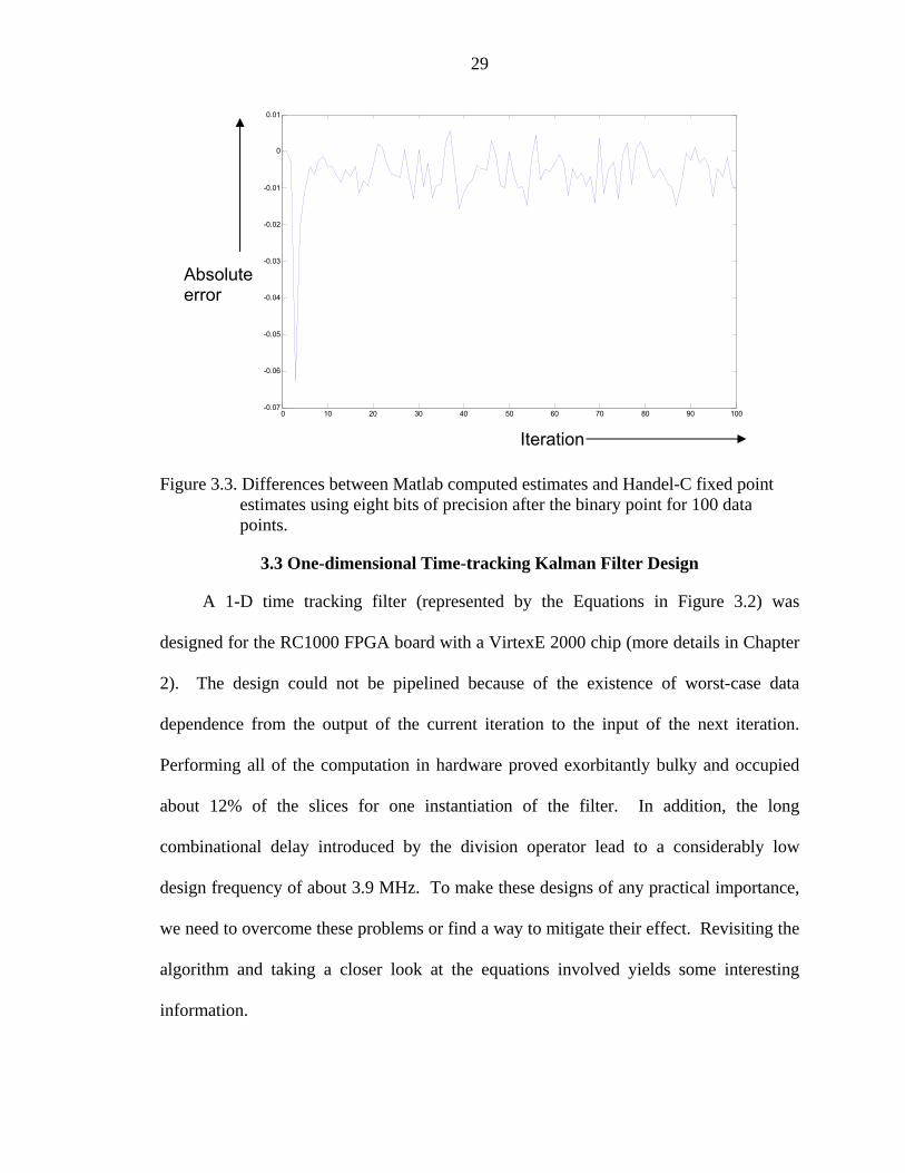
Figure 3.3. Differences between Matlab computed estimates and Handel-C fixed point estimates using eight bits of precision after the binary point for 100 data points.
3.3 One-dimensional Time-tracking Kalman Filter Design
A 1-D time tracking filter (represented by the Equations in Figure 3.2) was
designed for the RC1000 FPGA board with a VirtexE 2000 chip (more details in Chapter
2). The design could not be pipelined because of the existence of worst-case data
dependence from the output of the current iteration to the input of the next iteration.
Performing all of the computation in hardware proved exorbitantly bulky and occupied
about 12% of the slices for one instantiation of the filter. In addition, the long
combinational delay introduced by the division operator lead to a considerably low
design frequency of about 3.9 MHz. To make these designs of any practical importance,
we need to overcome these problems or find a way to mitigate their effect. Revisiting the
algorithm and taking a closer look at the equations involved yields some interesting
information.
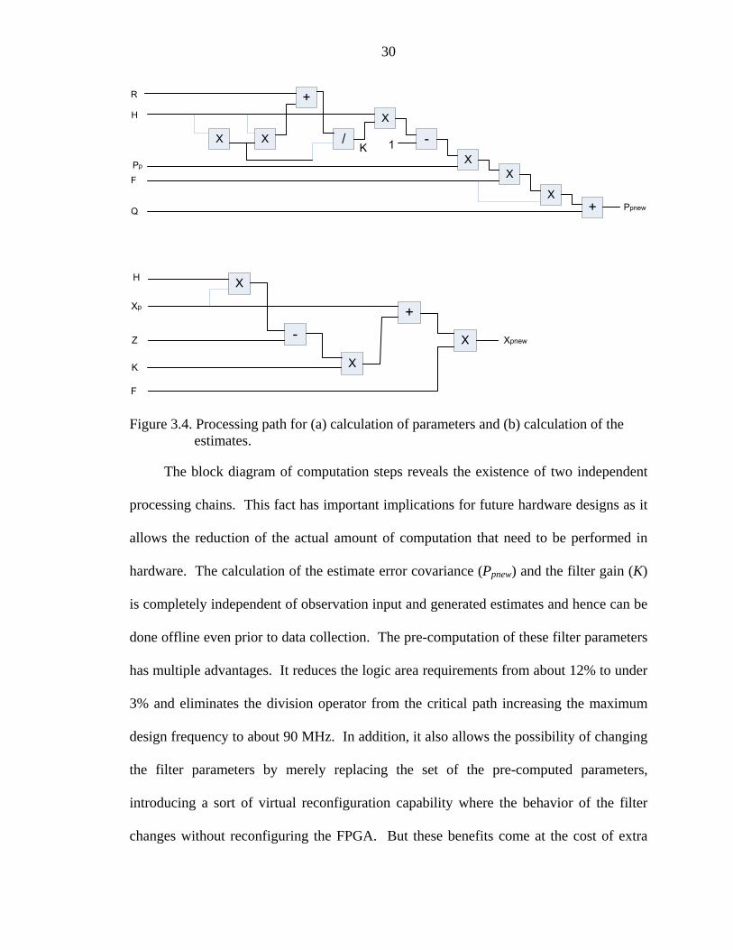
30
X X
+
/X
-X
X
X+
R
H
Pp
F
Q
K 1
Ppnew
X
-
X
+
X Xpnew
H
Xp
Z
K
F
Figure 3.4. Processing path for (a) calculation of parameters and (b) calculation of the estimates.
The block diagram of computation steps reveals the existence of two independent
processing chains. This fact has important implications for future hardware designs as it
allows the reduction of the actual amount of computation that need to be performed in
hardware. The calculation of the estimate error covariance (Ppnew) and the filter gain (K)
is completely independent of observation input and generated estimates and hence can be
done offline even prior to data collection. The pre-computation of these filter parameters
has multiple advantages. It reduces the logic area requirements from about 12% to under
3% and eliminates the division operator from the critical path increasing the maximum
design frequency to about 90 MHz. In addition, it also allows the possibility of changing
the filter parameters by merely replacing the set of the pre-computed parameters,
introducing a sort of virtual reconfiguration capability where the behavior of the filter
changes without reconfiguring the FPGA. But these benefits come at the cost of extra
31
memory requirements for storage of the filter parameters, a trade-off that was mentioned
earlier. The reduction in area is an important consideration for the 2-D filter design as it
allows a larger number of pixels to be processed in parallel. With these modifications a
1-D filter was developed for the RC1000 board and performance experiments were
conducted with data sets containing 600 data points. The latency incurred for transferring
all the values, one byte at a time, over the PCI bus hampers the performance. To
overcome this limitation, DMA is used to transfer all the data values onto the on-board
SRAM. The performance results for both the DMA and non-DMA case are shown in
Table 3.3 below and compared against Matlab results. The timing results in Matlab
yielded variations in multiple trials (which is attributed to the way Matlab works
internally and handles memory). For this reason further experiments were performed
using a C-based solution for obtaining software execution times.
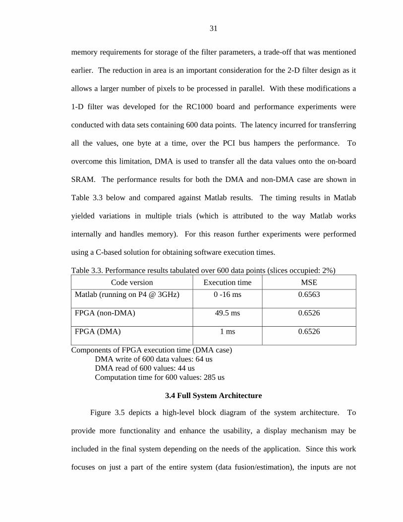
Table 3.3. Performance results tabulated over 600 data points (slices occupied: 2%) Code version Execution time MSE
Matlab (running on P4 @ 3GHz) 0 -16 ms 0.6563
FPGA (non-DMA) 49.5 ms 0.6526
FPGA (DMA) 1 ms 0.6526
Components of FPGA execution time (DMA case) DMA write of 600 data values: 64 us DMA read of 600 values: 44 us Computation time for 600 values: 285 us
3.4 Full System Architecture
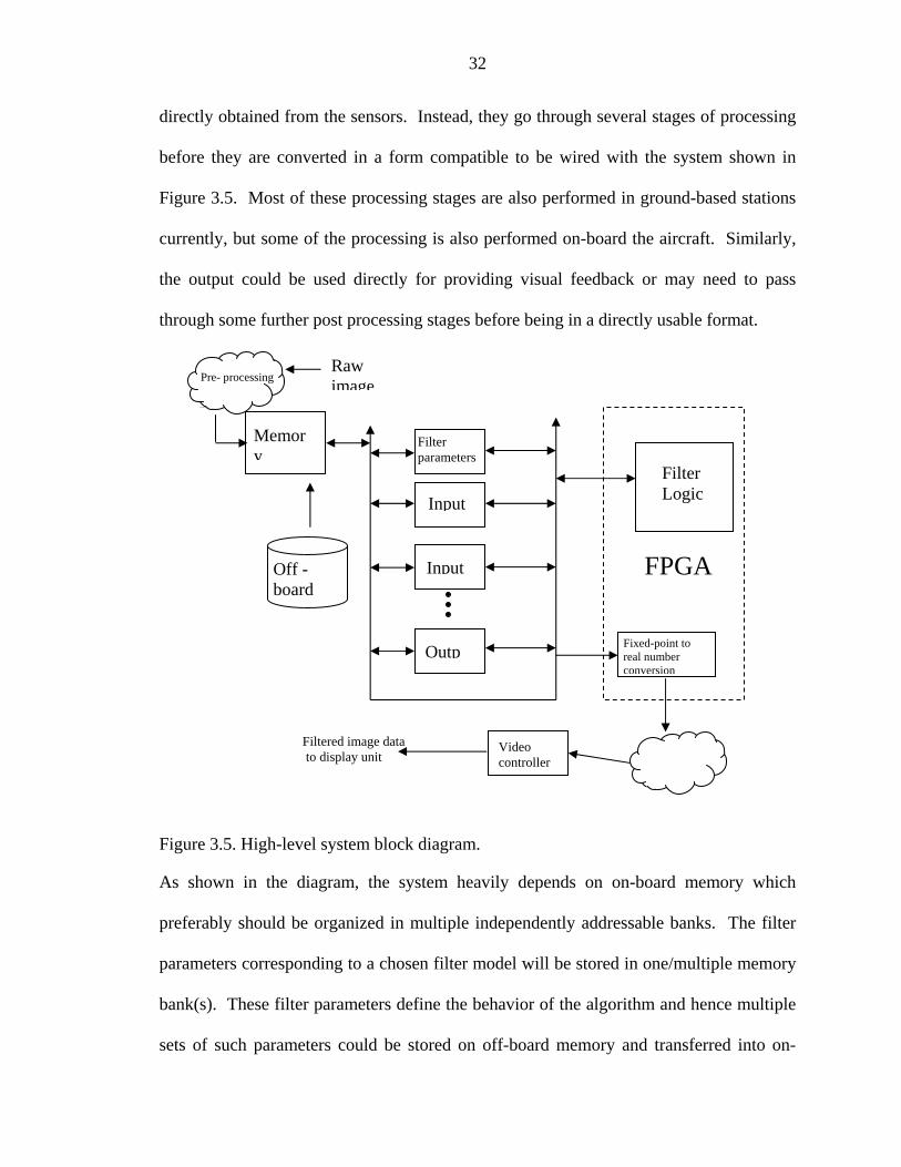
Figure 3.5 depicts a high-level block diagram of the system architecture. To
provide more functionality and enhance the usability, a display mechanism may be
included in the final system depending on the needs of the application. Since this work
focuses on just a part of the entire system (data fusion/estimation), the inputs are not
32
directly obtained from the sensors. Instead, they go through several stages of processing
before they are converted in a form compatible to be wired with the system shown in
Figure 3.5. Most of these processing stages are also performed in ground-based stations
currently, but some of the processing is also performed on-board the aircraft. Similarly,
the output could be used directly for providing visual feedback or may need to pass
through some further post processing stages before being in a directly usable format.
Raw image
Figure 3.5. High-level system block diagram.
As shown in the diagram, the system heavily depends on on-board memory which
preferably should be organized in multiple independently addressable banks. The filter
parameters corresponding to a chosen filter model will be stored in one/multiple memory
bank(s). These filter parameters define the behavior of the algorithm and hence multiple
sets of such parameters could be stored on off-board memory and transferred into on-
Filter parameters
Input
Input
Outp
Memory
Filter Logic
Fixed-point to real number conversion
Video controller
Filtered image data to display unit
FPGA
Pre- processing
Off - board
33
board memory as needed. The input image coming from one of the pre-processing
blocks is distributed in one of the multiple memory blocks reserved for input by a
memory controller. The provision of multiple input banks allows the overlapping input
data transfer time with the computation time of the previous set of data. Spreading the
filter parameters in multiple banks also aids in reducing the computation time by
allowing multiple parameters to be read in parallel. The test system on which all the
experiments are performed consists of a PCI-based card residing in a conventional Linux
Server. Hence it may not exactly mirror the system just outlined, and could involve some
additional issues such as limited memory, input/output transfer latencies over the PCI
bus, etc. The goals of this work include identifying limitations in the current systems that
hamper the performance, and speculating additional features that can enhance the
efficiency of the system, on the basis of the results obtained from experiments.
CHAPTER 4 MULTISCALE FILTER DESIGN AND RESULTS
This chapter presents different hardware designs developed for the multiscale
Kalman filter. Each subsequent design explores the opportunity to further improve
performance and builds on the shortcomings discovered in the previous design. Results
of the timing experiments are presented and analyzed to assess performance bottlenecks.
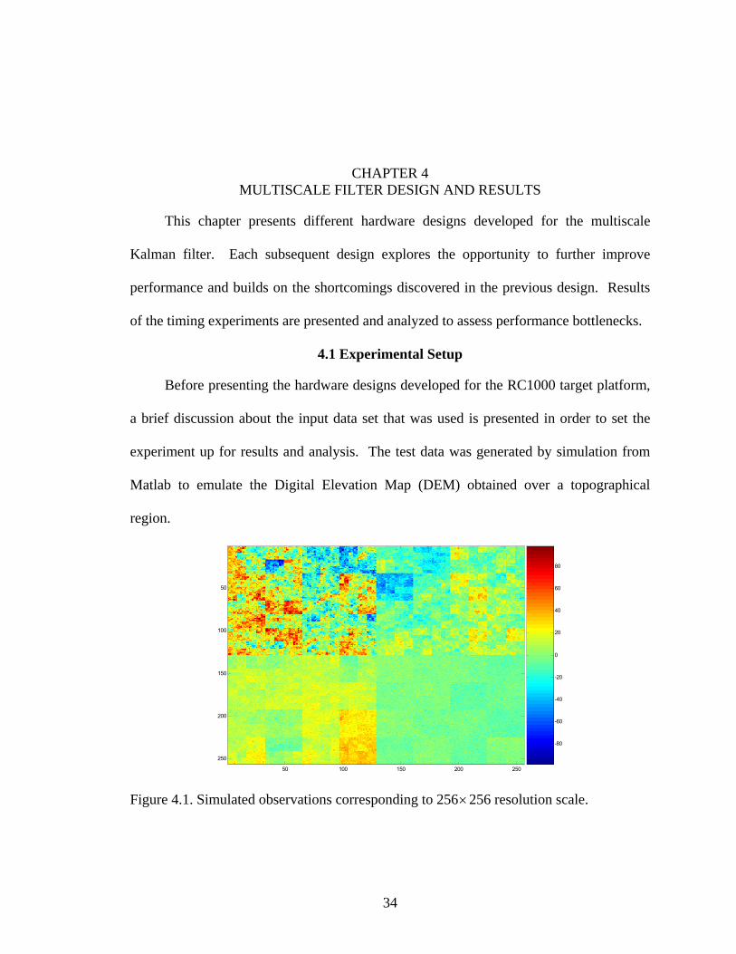
4.1 Experimental Setup
Before presenting the hardware designs developed for the RC1000 target platform,
a brief discussion about the input data set that was used is presented in order to set the
experiment up for results and analysis. The test data was generated by simulation from
Matlab to emulate the Digital Elevation Map (DEM) obtained over a topographical
region.
50 100 150 200 250
50
100
150
200
250
-80
-60
-40
-20
0
20
40
60
80
Figure 4.1. Simulated observations corresponding to 256×256 resolution scale.
34

35
The highest resolution observation was chosen to have a support of 256×256 pixels and
represents the data set corresponding to the one generated by an ALSM sensor. This
image resolution hence gives rise to nine scales in the quad tree structure. Another set of
observations was generated for a more coarse scale having a support of 128×128
representing the data generated from INSAR. Figure 4.1 depicts the (finer scale) data set,
which can be seen to have four varying level of roughness for different regions of the
image. Such a structure was chosen to incorporate the data corresponding to different
kinds of terrains such as plain grasslands (smooth) and sparse forests (rough) in a single
data set. This structure of the simulated observation was created by following the
fractional Brownian model and populating the nodes in the quad tree structure starting
from the root node using equations from Section 2.2.1. As with the case of 1-D filtering,
pre-computation is employed in this case as well to reduce the resource requirements.
Hence, the filter parameters needed for the online computation of estimates are also
generated using equations in Section 2.2.1 (namely )/(),/(),(),(),( αssPssPsFsCsK + ).
The parameters along with the observation set required approximately 870 KB of
memory when represented in the 8.8 fixed-point format. The small footprint of data, fed
as input to the FPGA, provides several opportunities of exploiting the on-board memory
in different ways as demonstrated further in the chapter. Some designs might require
additional storage because of details of the architecture. It is also worth noting that the
structure of computations in the 2-D filter though similar to the 1-D case has extra
operations due to the merge step involved for combining the child nodes into a parent
pixel.
36
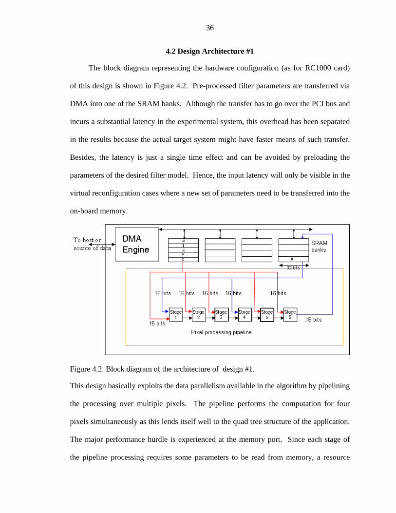
4.2 Design Architecture #1
The block diagram representing the hardware configuration (as for RC1000 card)
of this design is shown in Figure 4.2. Pre-processed filter parameters are transferred via
DMA into one of the SRAM banks. Although the transfer has to go over the PCI bus and
incurs a substantial latency in the experimental system, this overhead has been separated
in the results because the actual target system might have faster means of such transfer.
Besides, the latency is just a single time effect and can be avoided by preloading the
parameters of the desired filter model. Hence, the input latency will only be visible in the
virtual reconfiguration cases where a new set of parameters need to be transferred into the
on-board memory.
Figure 4.2. Block diagram of the architecture of design #1.
This design basically exploits the data parallelism available in the algorithm by pipelining
the processing over multiple pixels. The pipeline performs the computation for four
pixels simultaneously as this lends itself well to the quad tree structure of the application.
The major performance hurdle is experienced at the memory port. Since each stage of
the pipeline processing requires some parameters to be read from memory, a resource

37
conflict exists. Hence, a stall is required after every stage of computation which
effectively breaks down the pipeline and its associated advantages to a large extent.
Table 4.1 compares the processing time for the algorithm on a 2.4 GHz Xeon processor
with the time on the RC1000 board. The FPGA on the board is clocked at 30 MHz, and
better performance can be obtained by increasing the design clock, which can be
achieved by using faster, more advanced chips and by further optimizing the design.
Table 4.1. Performance comparison of a processor with an FPGA configured with design #1.
Execution time on Single scale (256×256) Multiple scales (till 4×4)
RC1000 15.14ms 20.5ms
2.4 GHz Xeon Processor 9.85ms 13.49ms
DMA latency for sending the data over the PCI bus: 1 scale (650KB): 3.1ms All scales (870KB approx): 3.9ms
Resource Utilization: Slices : 3286 out of 19200 (17%)Memory : 850KB approx. (filter parameters) : 170KB approx. (outputs)
The times are compared for both single and multiple scales of processing. The
computation is terminated when the image support reduces to just 4×4 because the
overheads dominate actual computation time. The amount of resources occupied by this
configuration is also listed beside the table. With just 17% of logic utilization for the
processing of four pixels, enough area is left to provide the opportunity for increasing the
amount of concurrent computation by adding more pixels in the processing chain. The
values in the table show that the FPGA-based filter performs about 1.5 times faster than a
conventional processor. In the embedded system arena the absolute performance of a
system is less relevant than the performance per cost and is considered as a better metric
for comparison. Similarly, raw performance improvements might not result in an order
of magnitude speedup, but they do come at about one hundredth of the running cost of a

38
competing system. The lessons learned from this design point to the fact that memory
bandwidth is a crucial factor for obtaining better performance for the application. The
resource hazards need to be eliminated to take complete advantage of the pipelined
structure.
The previous discussion related to the Kalman filtering involved in the application
which populates the nodes on the tree going upwards. This application also involves a
smoothing step to generate the estimates while traversing the tree from top to bottom.
Recursive application of the filtering pipeline generates multiple sets of estimates at
different scales, which are then used by the computations in the second step. The
structure of calculations involved is similar to the filtering step, but requires some
intermediate data values to be saved in addition to the outputs as in the previous case.
This further increases the memory bandwidth demands of the system, but since these
calculations only begin after the completion of the upwards step, they are not in conflict.
Figure 4.3 shows the modifications required to incorporate these effects. The additional
data has been stored in the empty memory banks, which allows them to be read in
parallel for the “smoothing” pipeline without any stall cycles.
Figure 4.3. Block diagram for the architecture of both the Kalman filter and smoother.
39
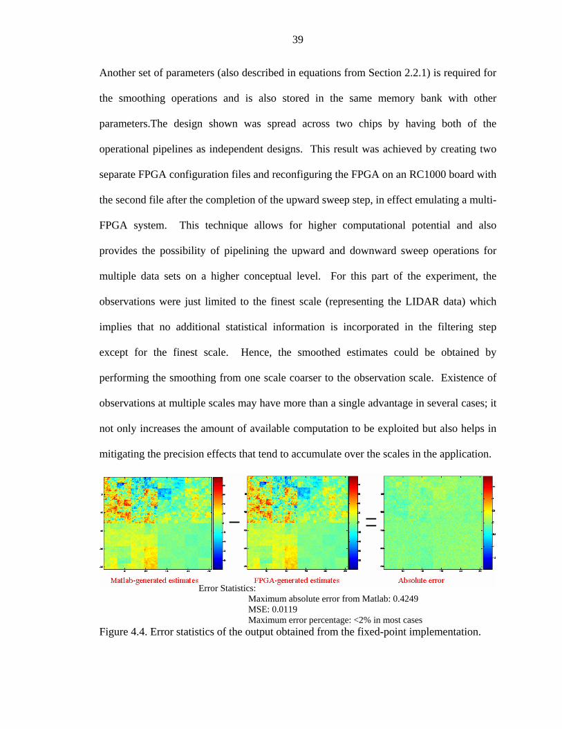
Another set of parameters (also described in equations from Section 2.2.1) is required for
the smoothing operations and is also stored in the same memory bank with other
parameters.The design shown was spread across two chips by having both of the
operational pipelines as independent designs. This result was achieved by creating two
separate FPGA configuration files and reconfiguring the FPGA on an RC1000 board with
the second file after the completion of the upward sweep step, in effect emulating a multi-
FPGA system. This technique allows for higher computational potential and also
provides the possibility of pipelining the upward and downward sweep operations for
multiple data sets on a higher conceptual level. For this part of the experiment, the
observations were just limited to the finest scale (representing the LIDAR data) which
implies that no additional statistical information is incorporated in the filtering step
except for the finest scale. Hence, the smoothed estimates could be obtained by
performing the smoothing from one scale coarser to the observation scale. Existence of
observations at multiple scales may have more than a single advantage in several cases; it
not only increases the amount of available computation to be exploited but also helps in
mitigating the precision effects that tend to accumulate over the scales in the application.
Figure 4.4. Error stati
Error Statistics: Maximum absolute error from Matlab: 0.4249 MSE: 0.0119 Maximum error percentage: <2% in most cases
stics of the output obtained from the fixed-point implementation.
40
The entire application, consisting of both the filtering and smoothing step, requires a total
of about 23% (17% for filtering + 6% for smoothing) of the slices, processing four pixels
simultaneously. Figure 4.4 compares the outputs obtained from the hardware version
with the MATLAB double-precision, floating-point results.
Because of the similarity in the structure of the two processing steps and the extra
memory demands posed on the system by including both of them, the follow-on designs
just focus on the filtering part of the application. A simplistic approach of improving the
performance that follows from the previous filter design is created by extending the
architecture to process more pixels in parallel, in effect filling up the unused area on the
chip. The problem that hinders the performance gain is the set of input parameters that
are required to process more pixels. Increasing the number of concurrent pixels further
increases the memory I/O demands. As a result, extra stall cycles are needed to read the
input values. These stall cycles, which are a major overhead, become a dominant part of
the computation time and quickly saturate the performance of the entire system. This
issue can be clearly understood by taking a closer look at the operational pipeline from
the Handel-C code:
Main loop of application takes 17 cycles of execution for 4 pixels of which just 7 cycles perform actual computation. Therefore, CCs for execution of: 4 pixels pipeline: 17×128 = (7 + 10) × (256/2) 8 pixels pipeline: 27×64 = (7 + 20)× (256/4) 16 pixels pipeline: 47×32 = (7 + 40) × (256/8)
Hence for 4n replication of pipeline: ( ) ( )nfn
n =⎟⎠⎞
⎜⎝⎛×+
2256107
Slope of the curve = ( ) 2414n
nf −=′
41
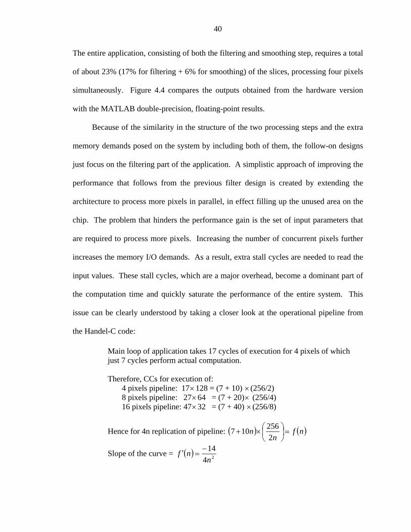
The same information is also conveyed in graphical form in Figure 4.5. As expected, the
resource requirements increase linearly with the pixel count but the performance does
not. These limitations need to be circumvented in the next design to further improve the
performance by a better pipeline which has less stall cycles, in effect exposing more
parallelism and hiding the input latency. There are two memory banks that were not
utilized in the current design which could be employed to increase the memory
bandwidth.
Performance Analysis
0
2
4
6
8
10
12
4 8 16
# of pixels processed in parallel
Tim
e (m
s)
0
0.5
1
1.5
2
2.5
Spee
dup
Execution Time Speedup Vs Processor
Slices occupied
4 pixels 17% 8 pixels 31% 16 pixels 64%
FPGA Resource Utilization:
Figure 4.5 Performance improvement and change in resource requirements with increase in concurrent computation.
4.2 Design Architecture #2
This design provides the FPGA-based engine with a higher memory bandwidth by
using all four on-board memory banks (i.e. 32×4 = 128 bits per CC) in an attempt to
eliminate the resource hazards present in the previous design. The filter parameters are
now evenly spread across all the banks and hence a simultaneous read of all memory
ports provides all the needed inputs for processing a single pixel. The available data

42
parallelism is again exploited by pipelining the processing of independent pixels.
Without the existence of stalls, the pipeline produces a single estimate every clock cycle.
The constraint in the architecture comes from the fact that even all the memory banks
together can only support the inputs for one pixel calculation. Simultaneous operation on
multiple pixels requires some stall cycles to be introduced in the design again.
Figure 4.6. Block diagram of the architecture of design #2.
Timing experiments were performed with the same set of data and compared
against the processing time for C code running on a Xeon processor. These results are
presented in Table 4.2 along with resource consumption information.
Table 4.2. Comparison of the execution times on the FPGA with Xeon processor and resource requirements of the hardware configuration for design #2.
Execution time on Single scale (256×256) Multiple scales (till 4×4)
RC1000 15.14ms 20.5ms 2.4 GHz Xeon Processor 7.39ms 9.86ms Speedup 2.04 2.07
DMA latency for sending the data over the PCI bus:1 scale (650KB) : 10.2ms All scales (870KB approx) : 11.4ms * the amount of data that needs to be transferred is slightly larger because of the architecture details
Resource Utilization: Slices : 963 out of 19200 (5%) Memory : 1MB approx. (filter parameters)
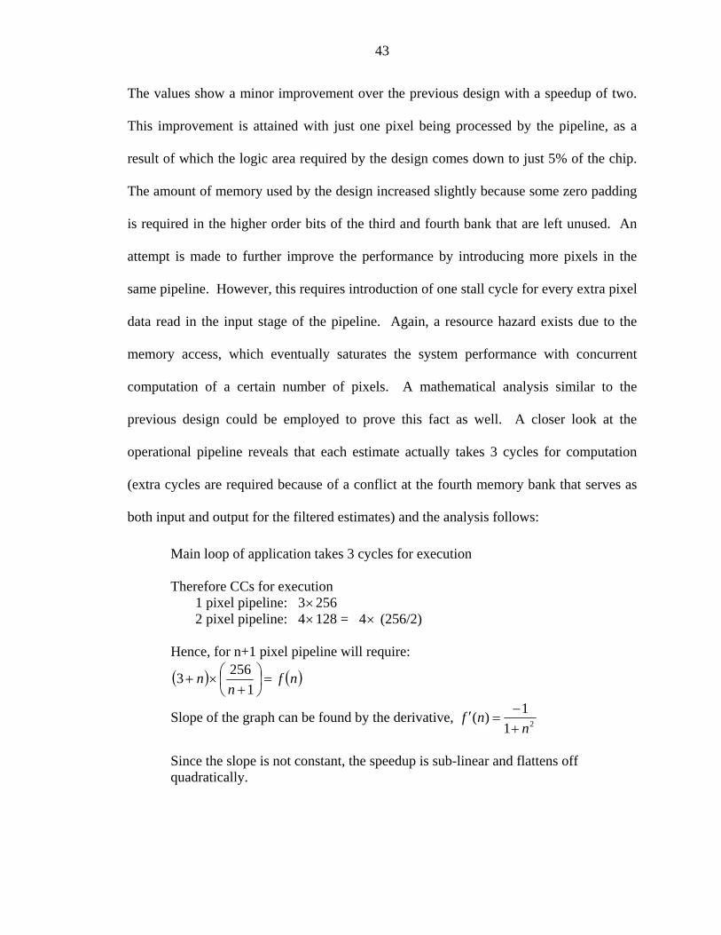
43
The values show a minor improvement over the previous design with a speedup of two.
This improvement is attained with just one pixel being processed by the pipeline, as a
result of which the logic area required by the design comes down to just 5% of the chip.
The amount of memory used by the design increased slightly because some zero padding
is required in the higher order bits of the third and fourth bank that are left unused. An
attempt is made to further improve the performance by introducing more pixels in the
same pipeline. However, this requires introduction of one stall cycle for every extra pixel
data read in the input stage of the pipeline. Again, a resource hazard exists due to the
memory access, which eventually saturates the system performance with concurrent
computation of a certain number of pixels. A mathematical analysis similar to the
previous design could be employed to prove this fact as well. A closer look at the
operational pipeline reveals that each estimate actually takes 3 cycles for computation
(extra cycles are required because of a conflict at the fourth memory bank that serves as
both input and output for the filtered estimates) and the analysis follows:
Main loop of application takes 3 cycles for execution Therefore CCs for execution 1 pixel pipeline: 3×256 2 pixel pipeline: 4×128 = 4× (256/2) Hence, for n+1 pixel pipeline will require:
( ) ( )nfn
n =⎟⎠⎞
⎜⎝⎛
+×+
12563
Slope of the graph can be found by the derivative, 211)(n
nf+−
=′
Since the slope is not constant, the speedup is sub-linear and flattens offquadratically.
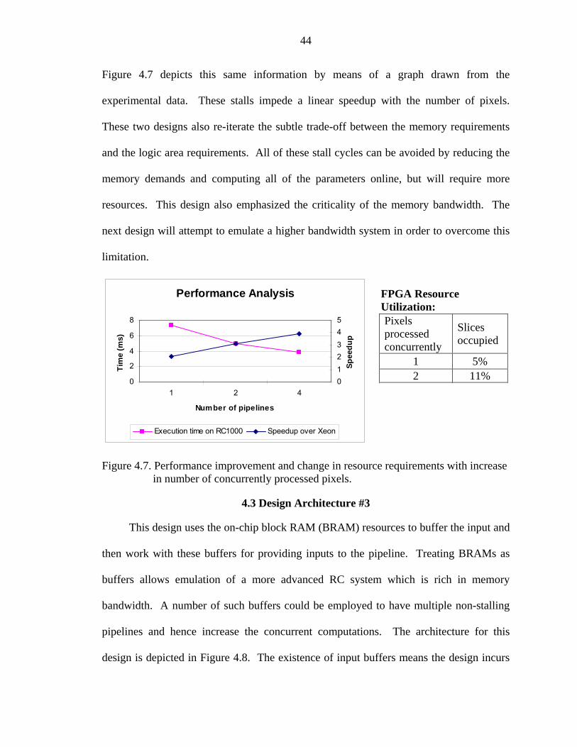
44
Figure 4.7 depicts this same information by means of a graph drawn from the
experimental data. These stalls impede a linear speedup with the number of pixels.
These two designs also re-iterate the subtle trade-off between the memory requirements
and the logic area requirements. All of these stall cycles can be avoided by reducing the
memory demands and computing all of the parameters online, but will require more
resources. This design also emphasized the criticality of the memory bandwidth. The
next design will attempt to emulate a higher bandwidth system in order to overcome this
limitation.
Performance Analysis
0
2
4
6
8
1 2 4
Number of pipelines
Tim
e (m
s)
012345
Spee
dup
Execution time on RC1000 Speedup over Xeon
Pixels processed concurrently
Slices occupied
1 5% 2 11%
FPGA Resource Utilization:
Figure 4.7. Performance improvement and change in resource requirements with increase in number of concurrently processed pixels.
4.3 Design Architecture #3
This design uses the on-chip block RAM (BRAM) resources to buffer the input and
then work with these buffers for providing inputs to the pipeline. Treating BRAMs as
buffers allows emulation of a more advanced RC system which is rich in memory
bandwidth. A number of such buffers could be employed to have multiple non-stalling
pipelines and hence increase the concurrent computations. The architecture for this
design is depicted in Figure 4.8. The existence of input buffers means the design incurs
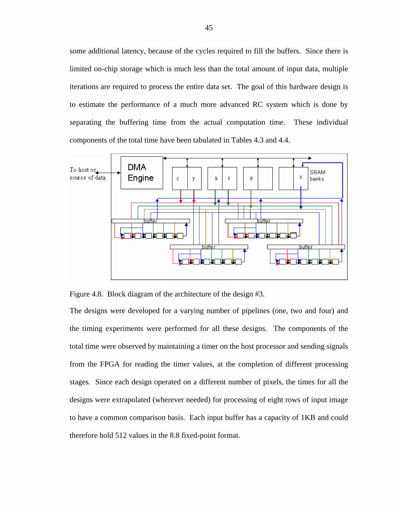
45
some additional latency, because of the cycles required to fill the buffers. Since there is
limited on-chip storage which is much less than the total amount of input data, multiple
iterations are required to process the entire data set. The goal of this hardware design is
to estimate the performance of a much more advanced RC system which is done by
separating the buffering time from the actual computation time. These individual
components of the total time have been tabulated in Tables 4.3 and 4.4.
Figure 4.8. Block diagram of the architecture of the design #3.
The designs were developed for a varying number of pipelines (one, two and four) and
the timing experiments were performed for all these designs. The components of the
total time were observed by maintaining a timer on the host processor and sending signals
from the FPGA for reading the timer values, at the completion of different processing
stages. Since each design operated on a different number of pixels, the times for all the
designs were extrapolated (wherever needed) for processing of eight rows of input image
to have a common comparison basis. Each input buffer has a capacity of 1KB and could
therefore hold 512 values in the 8.8 fixed-point format.
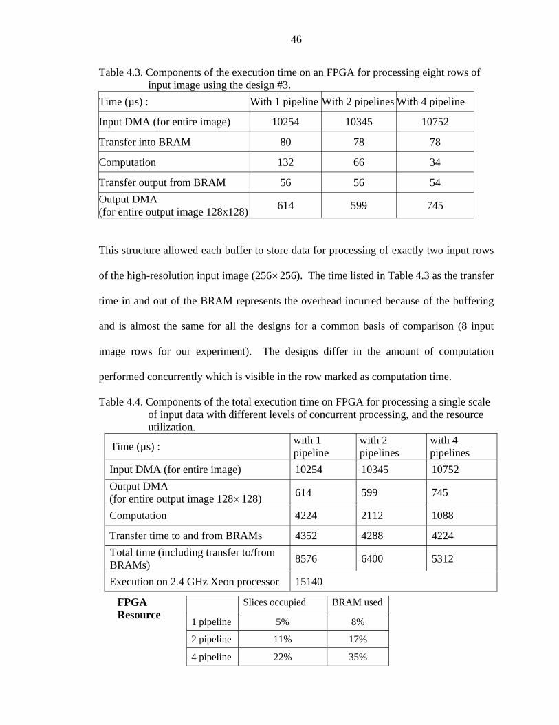
46
Table 4.3. Components of the execution time on an FPGA for processing eight rows of input image using the design #3.
Time (µs) : With 1 pipeline With 2 pipelines With 4 pipeline
Input DMA (for entire image) 10254 10345 10752
Transfer into BRAM 80 78 78
Computation 132 66 34
Transfer output from BRAM 56 56 54 Output DMA (for entire output image 128x128) 614 599 745
This structure allowed each buffer to store data for processing of exactly two input rows
of the high-resolution input image (256×256). The time listed in Table 4.3 as the transfer
time in and out of the BRAM represents the overhead incurred because of the buffering
and is almost the same for all the designs for a common basis of comparison (8 input
image rows for our experiment). The designs differ in the amount of computation
performed concurrently which is visible in the row marked as computation time.
Table 4.4. Components of the total execution time on FPGA for processing a single scale of input data with different levels of concurrent processing, and the resource utilization.
Time (µs) : with 1 pipeline
with 2 pipelines
with 4 pipelines
Input DMA (for entire image) 10254 10345 10752 Output DMA (for entire output image 128×128) 614 599 745
Computation 4224 2112 1088
Transfer time to and from BRAMs 4352 4288 4224 Total time (including transfer to/from BRAMs) 8576 6400 5312
Execution on 2.4 GHz Xeon processor 15140 FPGA
Resource Slices occupied BRAM used
1 pipeline 5% 8% 2 pipeline 11% 17% 4 pipeline 22% 35%
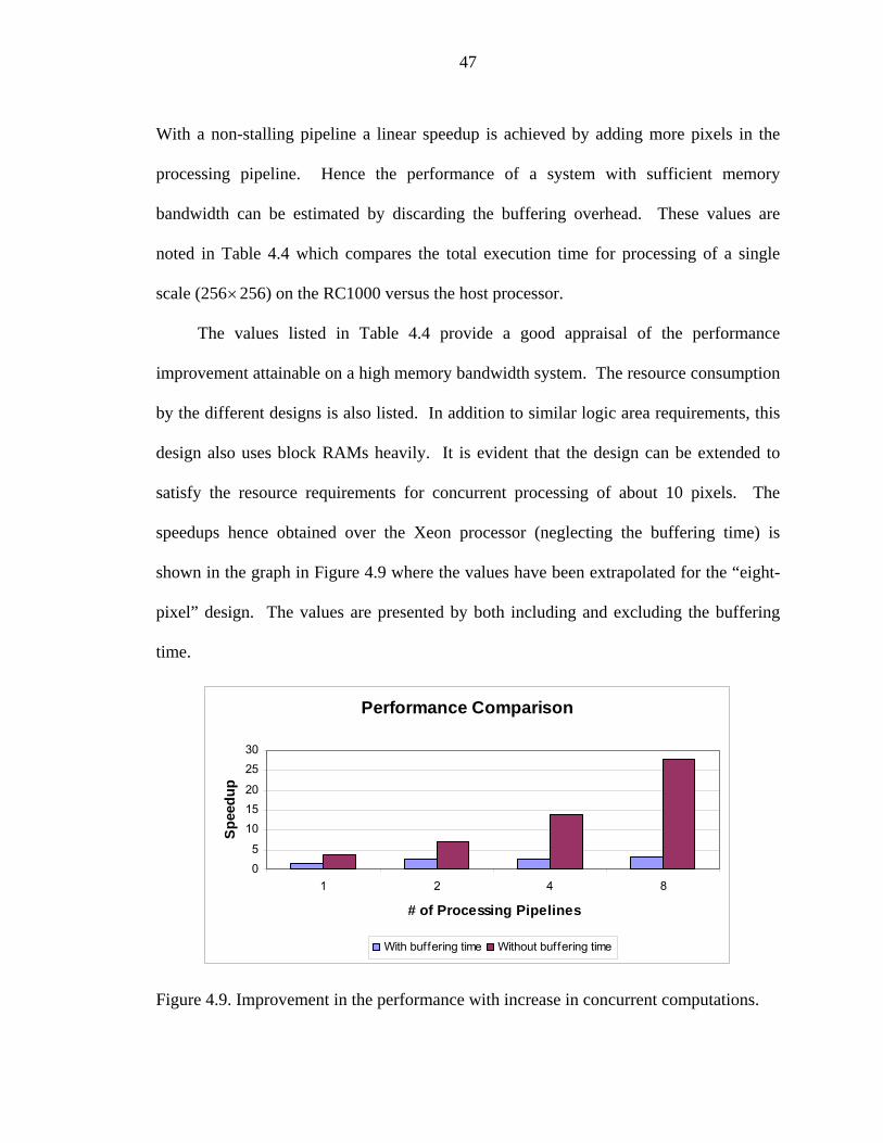
47
With a non-stalling pipeline a linear speedup is achieved by adding more pixels in the
processing pipeline. Hence the performance of a system with sufficient memory
bandwidth can be estimated by discarding the buffering overhead. These values are
noted in Table 4.4 which compares the total execution time for processing of a single
scale (256×256) on the RC1000 versus the host processor.
The values listed in Table 4.4 provide a good appraisal of the performance
improvement attainable on a high memory bandwidth system. The resource consumption
by the different designs is also listed. In addition to similar logic area requirements, this
design also uses block RAMs heavily. It is evident that the design can be extended to
satisfy the resource requirements for concurrent processing of about 10 pixels. The
speedups hence obtained over the Xeon processor (neglecting the buffering time) is
shown in the graph in Figure 4.9 where the values have been extrapolated for the “eight-
pixel” design. The values are presented by both including and excluding the buffering
time.
Performance Comparison
05
101520
2530
1 2 4 8
# of Processing Pipelines
Spee
dup
With buffering time Without buffering time
Figure 4.9. Improvement in the performance with increase in concurrent computations.
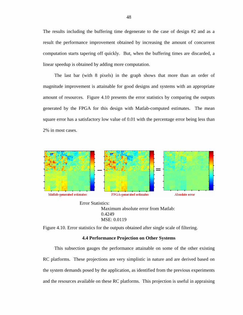
48
The results including the buffering time degenerate to the case of design #2 and as a
result the performance improvement obtained by increasing the amount of concurrent
computation starts tapering off quickly. But, when the buffering times are discarded, a
linear speedup is obtained by adding more computation.
The last bar (with 8 pixels) in the graph shows that more than an order of
magnitude improvement is attainable for good designs and systems with an appropriate
amount of resources. Figure 4.10 presents the error statistics by comparing the outputs
generated by the FPGA for this design with Matlab-computed estimates. The mean
square error has a satisfactory low value of 0.01 with the percentage error being less than
2% in most cases.
Error Statistics:
Maximum absolute error from Matlab: 0.4249 MSE: 0.0119
Figure 4.10. Error statistics for the outputs obtained after single scale of filtering.
4.4 Performance Projection on Other Systems
This subsection gauges the performance attainable on some of the other existing
RC platforms. These projections are very simplistic in nature and are derived based on
the system demands posed by the application, as identified from the previous experiments
and the resources available on these RC platforms. This projection is useful in appraising
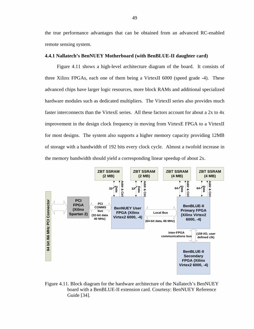
49
the true performance advantages that can be obtained from an advanced RC-enabled
remote sensing system.
4.4.1 Nallatech’s BenNUEY Motherboard (with BenBLUE-II daughter card)
Figure 4.11 shows a high-level architecture diagram of the board. It consists of
three Xilinx FPGAs, each one of them being a VirtexII 6000 (speed grade -4). These
advanced chips have larger logic resources, more block RAMs and additional specialized
hardware modules such as dedicated multipliers. The VirtexII series also provides much
faster interconnects than the VirtexE series. All these factors account for about a 2x to 4x
improvement in the design clock frequency in moving from VirtexE FPGA to a VirtexII
for most designs. The system also supports a higher memory capacity providing 12MB
of storage with a bandwidth of 192 bits every clock cycle. Almost a twofold increase in
the memory bandwidth should yield a corresponding linear speedup of about 2x.
PCI FPGA(Xilinx
Spartan 2)BenNUEY User
FPGA (Xilinx Virtex2 6000, -4)
ZBT SSRAM(2 MB)
ZBT SSRAM(2 MB)
BenBLUE-II Primary FPGA (Xilinx Virtex2
6000, -4)
ZBT SSRAM(4 MB)
ZBT SSRAM(4 MB)
BenBLUE-II Secondary
FPGA (Xilinx Virtex2 6000, -4)
Local Bus
64 b
it /6
6 M
Hz
PCI C
onne
ctor
Addr &
Ctrl
Data32
Addr &
Ctrl
Data32
Addr &
Ctrl
Data64
Addr &
Ctrl
Data64
(32-bit data40 MHz)
(64-bit data, 66 MHz)
Inter-FPGAcommunications bus
(159 I/O, user defined clk)
PCICOMMS
bus
Figure 4.11. Block diagram for the hardware architecture of the Nallatech’s BenNUEY board with a BenBLUE-II extension card. Courtesy: BenNUEY Reference Guide [34].
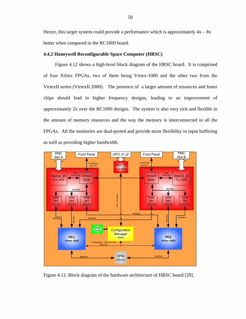
50
Hence, this target system could provide a performance which is approximately 4x – 8x
better when compared to the RC1000 board.
4.4.2 Honeywell Reconfigurable Space Computer (HRSC)
Figure 4.12 shows a high-level block diagram of the HRSC board. It is comprised
of four Xilinx FPGAs, two of them being Virtex-1000 and the other two from the
VirtexII series (VirtexII 2000). The presence of a larger amount of resources and faster
chips should lead to higher frequency designs, leading to an improvement of
approximately 2x over the RC1000 designs. The system is also very rich and flexible in
the amount of memory resources and the way the memory is interconnected to all the
FPGAs. All the memories are dual-ported and provide more flexibility in input buffering
as well as providing higher bandwidth.
PMCA_IFPLX 9054
DPMSB1
256x32
PE1Virtex 1000
PMCSlot A
PMCSlot B
Front Panel
VirtexII2000
VirtexII2000
DPMSB1
256x32
DPMSB2
256x32
DPM256x32
DPMSB2
256x32
ConfigurationManager
Virtex
DPMSB3
256x32
DPMSB3
256x32
Front Panel
PMCB_IFPLX 9054
cPC
I Loc
al B
us
MemBus
MemBus
MemBus
MemBusMemBus
Mem
Bus
Mem
Bus
MemBus MemBus
MemBus
PMCLocal Bus
PMCLocal Bus
Configuration, User I/O, andinterrupts
FrontPanelUser I/O
FrontPanelUser I/O
Config.Cache
cPCI_IFPLX 9054
cPCI J1,J2
PE2Virtex 1000
Figure 4.12. Block diagram of the hardware architecture of HRSC board [29].
51
A single HRSC board supports approximately 1.75GB of storage capacity with a
bandwidth of 448 bits per clock cycle. This high bandwidth should be more amenable to
the design and should yield a performance enhancement of about 4x. The HRSC board,
specifically tailored for space-based computing, was designed with similar considerations
and would therefore lead to a system-level performance improvement on the order of 8x
over the RC1000 card.
This chapter presented a detailed discussion of the various experiments conducted
and the results obtained. The next chapter summarizes the document by providing a set
of conclusion and future directions in which the work could be pursued.
CHAPTER 5 CONCLUSIONS AND FUTURE WORK
This chapter summarizes the findings of this research and draws conclusions based
on the results and observations presented in the previous chapters. It also discusses some
unfinished issues and tasks that can be pursued further to build a complete system and do
further analysis.
Most of the current remote-sensing systems rely on conventional processors for
performing computation offline after data acquisition and lack any real-time processing
capabilities. Future systems will need on-board high-performance computing facilities in
order to be able to perform increasing levels of computation. In such systems,
performance per unit cost is a much more important metric than raw performance. This
work has demonstrated a strong case depicting the relevance of reconfigurable computing
for performing fast on-board computation. Several hardware configurations have been
developed to extend the prior work on 1-D Kalman filtering to a 2-D case. The results
have shown over 25 times speedup in computation time in ideal scenarios compared to
the conventional GPP-based solutions which is bound to further increase with more
advanced and faster FPGAs. More than two orders of magnitude improvement can be
obtained on such advanced systems. Systems capable of yielding such high performance,
coupled with other attributes such as low power, cost and space requirements make them
a perfect match for remote sensing systems and can make airborne-based, real-time
processing possible. There has been a great deal of prior work done in the field of
mapping image processing algorithms on FPGA-based systems, but its application to the
52
53
remote sensing world is still in its infancy. The results obtained in this work, show
promise and demand further research and investigation.
This work also highlighted some key issues involved in the design of remote-
sensing applications for RC systems. Firstly, floating-point operations are wasteful of
resources when designed for hardware, whereas fixed-point operations are more
amenable in such cases. Therefore, algorithms need to be redesigned to mitigate the
quantization effects and tested to ensure that they provide a desired level of accuracy.
Secondly, remote-sensing applications pose high demands on the memory bandwidth of
the system. Hence, the target systems should support a high memory bandwidth in
addition to just providing large storage capacity for being successful. Use of multi-port
memories provides added advantages, allowing both reads and writes to take place in
parallel and providing an effective mechanism of hiding input latencies. Thirdly, the
ability of processing data in parallel is a key attribute for meeting real-time requirements
in a remote-sensing scenario, where multiple sensors produce large amounts of data at a
high rate. Different designs have been developed and analyzed as a part of this work that
exploit a high degree of parallelism and adapt to the available resources.
The designs presented in this work for the application use pre-computed parameters
which describe the behavior of the filter. Hence, they offer the ability of “virtual
reconfiguration,” which is a novel concept developed and introduced through the course
of this research, where the set of filter parameters in the memory could be changed to
adapt the filter behavior. This functionality has important implications in both the remote
sensing and RC arenas. Most remote-sensing systems need to adapt their processing
methods in response to the change in data statistics. Although current RC systems can
54
support dynamic reconfiguration of FPGAs, the configuration times are very slow, hence
virtual reconfiguration provides a faster mechanism to achieve the same effect.
To keep the work tractable the scope of the project was limited; only one part of the
entire process was dealt with in detail, leaving several other modules. Most importantly,
the raw sensor inputs have to go through several stages of processing before being
converted into a form compatible with the designs developed in this work. The design
and development of the pre-processing module needs to be addressed before an actual
system can be developed.
There were several lessons learned about the design of target hardware system and
how different resources affect the performance. The design of such a hardware system
based on the results and conclusions of this work is a challenging task that demands
attention. There has been recent interest in developing stand-alone, FPGA-based systems
which can exist without a host processor. Such a system offers a very cost-effective
solution for embedded environments. Adapting such systems to the needs of remote-
sensing application can have a monumental effect on the future research in this direction.
This work also shows projection of the performance on some advanced systems, which
need to be verified with experimental results.
The focus of this work was to analyze the feasibility of deploying RC systems in
the remote sensing arena and developing designs to support these claims, as a result the
designs developed in this work are not optimal. With more time and optimizations the
designs could yield better performance, for example by increasing the clock frequencies
of the designs, or providing direct DMA into the block RAMs to hide the input and
output latencies. As pointed out earlier, the use of fixed-point is very important for

55
economical hardware configurations, but it leads to quantization errors that can be high
enough to defeat the purpose of acceleration in some cases. There are several ways in
which these quantization effects of can be mitigated by changes in the algorithm, such as
normalization of all the parameters or providing observations at multiple scales to allow
the filter to overcome the effect of accumulation of errors. Exploring all the ways to
achieve this goal is essential for the success of the application.
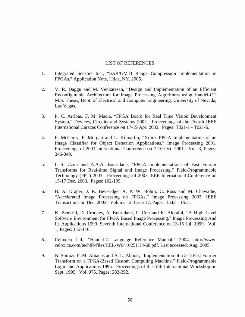
LIST OF REFERENCES
1. Integrated Sensors Inc., “SAR/GMTI Range Compression Implementation in FPGAs,” Application Note, Utica, NY, 2005.
2. V. R. Daggu and M. Venkatesan, “Design and Implementation of an Efficient Reconfigurable Architecture for Image Processing Algorithms using Handel-C,” M.S. Thesis, Dept. of Electrical and Computer Engineering, University of Nevada, Las Vegas.
3. P. C. Arribas, F. M. Macia, “FPGA Board for Real Time Vision Development System,” Devices, Circuits and Systems 2002. Proceedings of the Fourth IEEE International Caracas Conference on 17-19 Apr. 2002. Pages: T021-1 - T021-6.
4. P. McCurry, F. Morgan and L. Kilmartin, “Xilinx FPGA Implementation of an Image Classifier for Object Detection Applications,” Image Processing 2001. Proceedings of 2001 International Conference on 7-10 Oct. 2001. Vol. 3, Pages: 346-349.
5. I. S. Uzun and A.A.A. Bouridane, “FPGA Implementations of Fast Fourier Transforms for Real-time Signal and Image Processing,” Field-Programmable Technology (FPT) 2003. Proceedings of 2003 IEEE International Conference on 15-17 Dec. 2003. Pages: 102-109.
6. B. A. Draper, J. R. Beveridge, A. P. W. Böhm, C. Ross and M. Chawathe, “Accelerated Image Processing on FPGAs,” Image Processing 2003. IEEE Transactions on Dec. 2003. Volume 12, Issue 12, Pages: 1543 – 1551.
7. K. Benkrid, D. Crookes, A. Bouridane, P. Con and K. Alotaibi, “A High Level Software Environment for FPGA Based Image Processing,” Image Processing And Its Applications 1999. Seventh International Conference on 13-15 Jul. 1999. Vol. 1, Pages: 112-116.
8. Celoxica Ltd., “Handel-C Language Reference Manual,” 2004. http://www. celoxica.com/techlib/files/CEL-W0410251JJ4-60.pdf. Last accessed: Aug. 2005.
9. N. Shirazi, P. M. Athanas and A. L. Abbott, “Implementation of a 2-D Fast Fourier Transform on a FPGA-Based Custom Computing Machine,” Field-Programmable Logic and Applications 1995. Proceedings of the fifth International Workshop on Sept. 1995. Vol. 975, Pages: 282-292.
56
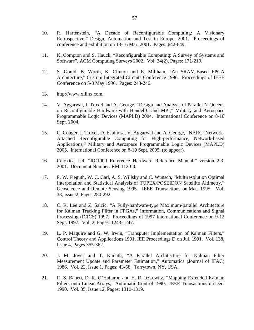
57
10. R. Hartenstein, “A Decade of Reconfigurable Computing: A Visionary Retrospective,” Design, Automation and Test in Europe, 2001. Proceedings of conference and exhibition on 13-16 Mar. 2001. Pages: 642-649.
11. K. Compton and S. Hauck, “Reconfigurable Computing: A Survey of Systems and Software”, ACM Computing Surveys 2002. Vol. 34(2), Pages: 171-210.
12. S. Gould, B. Worth, K. Clinton and E. Millham, “An SRAM-Based FPGA Architecture,” Custom Integrated Circuits Conference 1996. Proceedings of IEEE Conference on 5-8 May 1996. Pages: 243-246.
13. http://www.xilinx.com.
14. V. Aggarwal, I. Troxel and A. George, “Design and Analysis of Parallel N-Queens on Reconfigurable Hardware with Handel-C and MPI,” Military and Aerospace Programmable Logic Devices (MAPLD) 2004. International Conference on 8-10 Sept. 2004.
15. C. Conger, I. Troxel, D. Espinosa, V. Aggarwal and A. George, “NARC: Network-Attached Reconfigurable Computing for High-performance, Network-based Applications,” Military and Aerospace Programmable Logic Devices (MAPLD) 2005. International Conference on 8-10 Sept. 2005. (to appear).
16. Celoxica Ltd. “RC1000 Reference Hardware Reference Manual,” version 2.3, 2001. Document Number: RM-1120-0.
17. P. W. Fieguth, W. C. Carl, A. S. Willsky and C. Wunsch, “Multiresolution Optimal Interpolation and Statistical Analysis of TOPEX/POSEIDON Satellite Altimetry,” Geoscience and Remote Sensing 1995. IEEE Transactions on Mar. 1995. Vol. 33, Issue 2, Pages 280-292.
18. C. R. Lee and Z. Salcic, “A Fully-hardware-type Maximum-parallel Architecture for Kalman Tracking Filter in FPGAs,” Information, Communications and Signal Processing (ICICS) 1997. Proceedings of 1997 International Conference on 9-12 Sept. 1997. Vol. 2, Pages: 1243-1247.
19. L. P. Maguire and G. W. Irwin, “Transputer Implementation of Kalman Filters,” Control Theory and Applications 1991, IEE Proceedings D on Jul. 1991. Vol. 138, Issue 4, Pages 355-362.
20. J. M. Jover and T. Kailath, “A Parallel Architecture for Kalman Filter Measurement Update and Parameter Estimation,” Automatica (Journal of IFAC) 1986. Vol. 22, Issue 1, Pages: 43-58. Tarrytown, NY, USA.
21. R. S. Baheti, D. R. O’Hallaron and H. R. Itzkowitz, “Mapping Extended Kalman Filters onto Linear Arrays,” Automatic Control 1990. IEEE Transactions on Dec. 1990. Vol. 35, Issue 12, Pages: 1310-1319.
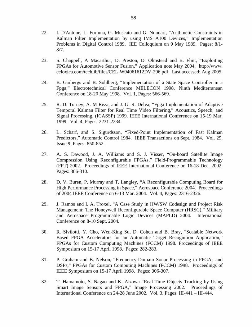
58
22. I. D'Antone, L. Fortuna, G. Muscato and G. Nunnari, “Arithmetic Constraints in Kalman Filter Implementation by using IMS A100 Devices,” Implementation Problems in Digital Control 1989. IEE Colloquium on 9 May 1989. Pages: 8/1-8/7.
23. S. Chappell, A Macarthur, D. Preston, D. Olmstead and B. Flint, “Exploiting FPGAs for Automotive Sensor Fusion,” Application note May 2004. http://www. celoxica.com/techlib/files/CEL-W04061612DV-296.pdf. Last accessed: Aug 2005.
24. B. Garbergs and B. Sohlberg, “Implementation of a State Space Controller in a Fpga,” Electrotechnical Conference MELECON 1998. Ninth Mediterranean Conference on 18-20 May 1998. Vol. 1, Pages: 566-569.
25. R. D. Turney, A. M Reza, and J. G. R. Delva, “Fpga Implementation of Adaptive Temporal Kalman Filter for Real Time Video Filtering,” Acoustics, Speech, and Signal Processing, (ICASSP) 1999. IEEE International Conference on 15-19 Mar. 1999. Vol. 4, Pages: 2231-2234.
26. L. Scharf, and S. Sigurdsson, “Fixed-Point Implementation of Fast Kalman Predictors,” Automatic Control 1984. IEEE Transactions on Sept. 1984. Vol. 29, Issue 9, Pages: 850-852.
27. A. S. Dawood, J. A. Williams and S. J. Visser, “On-board Satellite Image Compression Using Reconfigurable FPGAs,” Field-Programmable Technology (FPT) 2002. Proceedings of IEEE International Conference on 16-18 Dec. 2002. Pages: 306-310.
28. D. V. Buren, P. Murray and T. Langley, “A Reconfigurable Computing Board for High Performance Processing in Space,” Aerospace Conference 2004. Proceedings of 2004 IEEE Conference on 6-13 Mar. 2004. Vol. 4, Pages: 2316-2326.
29. J. Ramos and I. A. Troxel, “A Case Study in HW/SW Codesign and Project Risk Management: The Honeywell Reconfigurable Space Computer (HRSC),” Military and Aerospace Programmable Logic Devices (MAPLD) 2004. International Conference on 8-10 Sept. 2004.
30. R. Sivilotti, Y. Cho, Wen-King Su, D. Cohen and B. Bray, “Scalable Network Based FPGA Accelerators for an Automatic Target Recognition Application,” FPGAs for Custom Computing Machines (FCCM) 1998. Proceedings of IEEE Symposium on 15-17 April 1998. Pages: 282-283.
31. P. Graham and B. Nelson, “Frequency-Domain Sonar Processing in FPGAs and DSPs,” FPGAs for Custom Computing Machines (FCCM) 1998. Proceedings of IEEE Symposium on 15-17 April 1998. Pages: 306-307.
32. T. Hamamoto, S. Nagao and K. Aizawa “Real-Time Objects Tracking by Using Smart Image Sensors and FPGA,” Image Processing 2002. Proceedings of International Conference on 24-28 June 2002. Vol. 3, Pages: III-441 – III-444.

59
33. A. Utgikar and G. Seetharaman, “FPGA Implementable Architecture for Geometric Global Positioning,” Field-Programmable Technology (FPT) 2003. Proceedings of IEEE International Conference on 15-17 Dec. 2003. Pages: 451-455
34. Nallatech Inc. “BenNUEY Reference Guide,” Issue 10, 2004. Document Number: NT107-0123.

BIOGRAPHICAL SKETCH
Vikas Aggarwal received a Bachelor of Science degree in electronics and
communication engineering from the department of ECE at Guru Gobind Singh
Indraprastha University, India, in August of 2003. He moved over to United States to
pursue his graduate studies in the department of Electrical and Computer Engineering at
the University of Florida.
Vikas has been a paid graduate research assistant under the direction of Dr. Clint
Slatton in Adaptive Signal Processing Lab and under Dr. Alan George in High-
Performance Computing and Simulation Lab. Since becoming a paid graduate assistant
he has worked on numerous projects in two relatively different fields of reconfigurable
computing and adaptive signal processing techniques as applied to remote sensing
applications.
60