Embed Size (px)
Citation preview

Removal of single point diamond-turning marksby abrasive jet polishing
Z. Z. Li,1,* J. M. Wang,1 X. Q. Peng,1 L. T. Ho,2 Z. Q. Yin,1 S. Y. Li,1 and C. F. Cheung2
1National University of Defense Technology, DeYa, Changsha, Hunan Province 410073, China2Advanced Optics Manufacturing Centre, Department of Industrial and Systems Engineering,
The Hong Kong Polytechnic University, Hung Hom, Kowloon, 00852, Hong Kong
*Corresponding author: [email protected]
Received 18 November 2010; revised 22 February 2011; accepted 3 April 2011;posted 5 April 2011 (Doc. ID 138426); published 27 May 2011
Single point diamond turning (SPDT) is highly controllable and versatile in producing axially symmetricforms, non-axially-symmetric forms, microstructured surfaces, and free forms. However, the fine SPDTmarks left in the surface limit its performance, and they are difficult to reduce or eliminate. It is un-practical for traditional methods to remove the fine marks without destroying their forms, especiallyfor the aspheres and free forms. This paper introduces abrasive jet polishing (AJP) for the posttreatmentof diamond-turned surfaces to remove the periodic microstructures. Samples of diamond-turned electro-less nickel plated plano mirror were used in the experiments. One sample with an original surface rough-ness of more than 400nm decreased to 4nm after two iterations abrasive jet polishing; the surfaceroughness of another sample went from 3:7nm to 1:4nm after polishing. The periodic signatures on bothof the samples were removed entirely after polishing. Contrastive experimental research was carried outon electroless nickel mirror with magnetorheological finishing, computer controlled optical surfacing,and AJP. The experimental results indicate that AJP is more appropriate in removing the periodic SPDTmarks. Also, a figure maintaining experiment was carried out with the AJP process; the uniform polish-ing process shows that the AJP process can remove the periodic turning marks without destroying theoriginal form. © 2011 Optical Society of AmericaOCIS codes: 220.0220, 220.4610, 220.5450.
1. Introduction
Single point diamond turning (SPDT), which is cate-gorized in ultraprecision micromachining technolo-gies, possesses nanometric edge sharpness, formreproducibility, and wear resistance. With the ra-pidly growing demand for precision components suchas optoelectronics products, Walter-type x-ray man-drels, and nonferrous metal mirrors, SPDT hasbecome increasingly important for the manufactureof quality optical components with micrometer tosubmicrometer form accuracy and surface roughnessin the nanometer range [1]. The main limitation hasbeen the resulting microstructure, which is calledSPDT marks and which produces a diffraction effect
and stray light. For this reason, many components,including x-ray mandrels in particular, are handpostpolished to achieve both the form and texture re-quired [2]. But hand postpolishing is extremely diffi-cult on aspheres and free forms, which leads to aninevitable trade-off between quality of the surfacetexture achieved and destruction of the surfacefigure. Consequently, a method to eliminate thediamond-turning marks without destroying the formcould be a required process going forward.
Many presently widely used polishing techniques,such as ion beam figuring (IBF), magnetorheologicalfinishing (MRF), and computer controlled opticalsurfacing (CCOS), are not very fit for SPDT mark re-moval. Ion beam figuring has a strong selectivity inthe polished materials, although it can produce asuperfine surface [3]. The commonly used SPDTmaterials, such as nonferrous metals (including
0003-6935/11/162458-06$15.00/0© 2011 Optical Society of America
2458 APPLIED OPTICS / Vol. 50, No. 16 / 1 June 2011

electroless nickel) and plastics, are not suitable forIBF. The same problems also exist with MRF andCCOS, for they can induce some nicks on the polishedsurfaces and destroy the forms, although they canremove the periodic signatures [4,5].
Abrasive jet polishing (AJP), as a novel determi-nistic precision optical manufacturing technique,was first presented by O. W. Fähnle at Delft Univer-sity of Technology in 1998 [6]. In the AJP process, thehomogeneously premixed polishing slurry is pumpedby a low-pressured pump and sprayed onto the work-piece through a special nozzle to achieve polishing.The performance of the AJP process can be controlledby the components, concentration, and jet pressure ofthe slurry and also by the relative position and anglebetween the nozzle and workpiece [7]. Comparedwith traditional polishing methods, the AJP processhas many advantages [8,9]. First, the slender jet willbe less restricted by the shape or space of the work-piece, and it will be suitable for polishing variouscomplex surfaces, especially for steep cavities.Second, the recycled polishing fluid will maintainthe constant temperature of the workpiece, and itwill weed out the machining debris automatically.Third, the slender jet will produce a very smallmachining spot and, consequently, has little edgeeffect, which is beneficial for polishing micro-optics.Finally, the tiny material removed can be controlledby an appropriate abrasive and particle size with theright flow velocity, which can produce highly precisesurface forms.
In the work reported in this paper, the AJP processhas been adopted to eliminate SPDTmarks on differ-ent electroless nickel coated samples. The experimen-tal results show that the AJP process can remove theperiodic marks without destroying the forms. Theseapplications will undoubtedly widen the use of singlepoint diamond turned surfaces, as well as improvingits performance in optical applications.
2. Experimental Setup
A. Seven-Axis Ultraprecision Freeform Polishing Machine
The AJP process investigation was conducted on aseven-axis ultraprecision computerized numericalcontrol optical polishing machine produced by ZeekoLtd. [10,11]. The machine contains three linear axesx, y, and z and four rotational axes A, B, C, and H. Itcan produce ultraprecise surfaces on a variety of op-tical materials and surface forms. Abrasive jet pol-ishing does not have any direct contact with theworkpiece. The slurry is ejected from the nozzle ata pressure no greater than 20 bars and attacks thesurface of workpiece.
B. Experimental Procedures
In the present study, all the samples are electrolessnickel coated on aluminum alloy substrates. Some ofthe samples will be roughly turned by SPDT with aroughness of hundreds of nanometers, while otherswill be finely turned with a roughness of less than
5nm. After diamond turning, there will be SPDTmarks appearing on the surfaces, and also a diffrac-tion effect. Then the samples will be uniformly po-lished by the AJP process to remove the periodicmarks left by the previous process. The marks onthe samples will also be polished with MRF andCCOS to contrast the results with the AJP process.Finally, a figure maintaining experiment with a uni-form AJP process will be carried out to validate itsfigure maintaining capability.
3. Machining Process
A. Single Point Diamond Turning
In SPDT, nonferrous metals and plastics are widelyused, among which electroless nickel of an amor-phous structure is one excellent material. In addi-tion, electroless nickel has also been widely usedin industrial and optical applications [12,13]. Inour experiments we prepared electroless nickel pla-ted on the plano aluminum alloy, A6061. Nickel plat-ing was done for eight hours, and the thickness of theelectroless nickel was approximately 100 μm. It con-tains about 10% phosphorus, which is widely used inthe electroless nickel area and also in the opticalapplication area, with an appropriate hardness formachining (the Vickers-hardness value equals about550). The SPDT parameters for rough samples andfine samples are given in Table 1.
B. Abrasive Jet Polishing
In the AJP process, the polishing liquid containing6wt:% abrasive grains of alumina (Al2O3) and otheradditives was used in the experiments. The diameterof the nozzle was 1mm. In our experiments a rasterpolishing path was chosen as the scanning mode,and the scanning step size was 0:2mm. Some of theparameters used in the experiments are given inTable 2.
Table 1. SPDT Parameters for Different Samples
Rough Samples Fine Samples
Spindle speed (rpm) 1000 1000Feed rate (mm=min) 10 5Depth of cut (μm) 5 1Radius of tool edge (mm) 0.54 0.54
Table 2. AJP Parameters for Different Samples
Rough Sample
FirstPolishing
SecondPolishing
FineSample
Incidence angle(degrees)
60 60 60
Jet pressure (bars) 10 5 3Particle size (μm) 1.5 1.5 1Incidence distance
(mm)10 10 10
Removal depth (μm) 0.8 0.2 0.2
1 June 2011 / Vol. 50, No. 16 / APPLIED OPTICS 2459
4. Results and Discussion
A. AJP Process
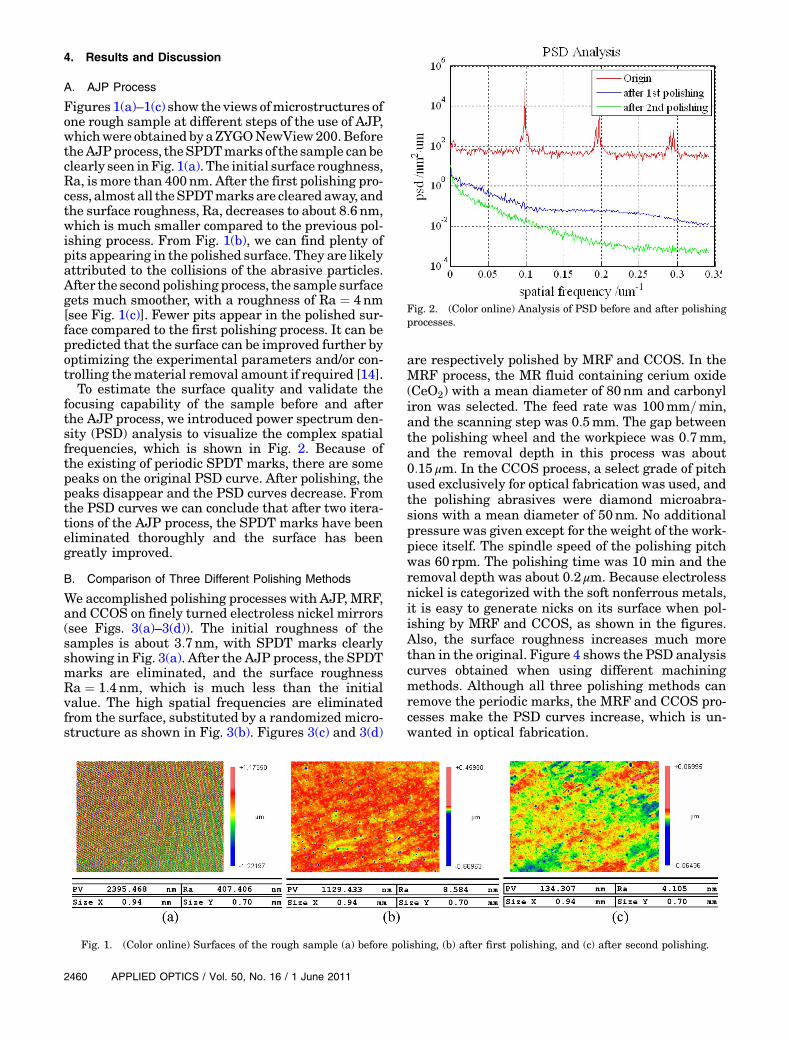
Figures 1(a)–1(c) show the views ofmicrostructures ofone rough sample at different steps of the use of AJP,whichwere obtained by aZYGONewView200.BeforetheAJPprocess, theSPDTmarks of the sample canbeclearly seen inFig. 1(a). The initial surface roughness,Ra, is more than 400nm. After the first polishing pro-cess, almost all theSPDTmarksare clearedaway, andthe surface roughness, Ra, decreases to about 8:6nm,which is much smaller compared to the previous pol-ishing process. From Fig. 1(b), we can find plenty ofpits appearing in the polished surface. They are likelyattributed to the collisions of the abrasive particles.After the secondpolishing process, the sample surfacegets much smoother, with a roughness of Ra ¼ 4nm[see Fig. 1(c)]. Fewer pits appear in the polished sur-face compared to the first polishing process. It can bepredicted that the surface can be improved further byoptimizing the experimental parameters and/or con-trolling thematerial removal amount if required [14].
To estimate the surface quality and validate thefocusing capability of the sample before and afterthe AJP process, we introduced power spectrum den-sity (PSD) analysis to visualize the complex spatialfrequencies, which is shown in Fig. 2. Because ofthe existing of periodic SPDT marks, there are somepeaks on the original PSD curve. After polishing, thepeaks disappear and the PSD curves decrease. Fromthe PSD curves we can conclude that after two itera-tions of the AJP process, the SPDT marks have beeneliminated thoroughly and the surface has beengreatly improved.
B. Comparison of Three Different Polishing Methods
We accomplished polishing processes with AJP, MRF,and CCOS on finely turned electroless nickel mirrors(see Figs. 3(a)–3(d)). The initial roughness of thesamples is about 3:7nm, with SPDT marks clearlyshowing in Fig. 3(a). After the AJP process, the SPDTmarks are eliminated, and the surface roughnessRa ¼ 1:4nm, which is much less than the initialvalue. The high spatial frequencies are eliminatedfrom the surface, substituted by a randomized micro-structure as shown in Fig. 3(b). Figures 3(c) and 3(d)
are respectively polished by MRF and CCOS. In theMRF process, the MR fluid containing cerium oxide(CeO2) with a mean diameter of 80nm and carbonyliron was selected. The feed rate was 100mm=min,and the scanning step was 0:5mm. The gap betweenthe polishing wheel and the workpiece was 0:7mm,and the removal depth in this process was about0:15 μm. In the CCOS process, a select grade of pitchused exclusively for optical fabrication was used, andthe polishing abrasives were diamond microabra-sions with a mean diameter of 50nm. No additionalpressure was given except for the weight of the work-piece itself. The spindle speed of the polishing pitchwas 60 rpm. The polishing time was 10 min and theremoval depth was about 0:2 μm. Because electrolessnickel is categorized with the soft nonferrous metals,it is easy to generate nicks on its surface when pol-ishing by MRF and CCOS, as shown in the figures.Also, the surface roughness increases much morethan in the original. Figure 4 shows the PSD analysiscurves obtained when using different machiningmethods. Although all three polishing methods canremove the periodic marks, the MRF and CCOS pro-cesses make the PSD curves increase, which is un-wanted in optical fabrication.
Fig. 1. (Color online) Surfaces of the rough sample (a) before polishing, (b) after first polishing, and (c) after second polishing.
Fig. 2. (Color online) Analysis of PSD before and after polishingprocesses.
2460 APPLIED OPTICS / Vol. 50, No. 16 / 1 June 2011

Also, contrastive experiments of convergence rateusing these three different polishing methods are in-vestigated. The experiments were carried out onroughly turned electroless nickel plano round mir-rors with diameters of 20mm. The parameters ofthese three polishing methods were the same asdescribed before. The experimental results are
shown in Fig. 5. They indicates that both the MRFand CCOS processes have a high convergence ratecompared to the AJP process. This is mainly dueto the high material removal rate of these two polish-ing methods. Though the convergence rate of the AJPprocess is low due to its relatively low materialremoval rate, it can obtain a much finer surface
Fig. 3. (Color online) Surfaces of fine samples (a) before polishing, (b) after AJP, (c) after MRF, and (d) after CCOS.
Fig. 4. (Color online) Analysis of PSD curves obtained by differ-ent machining methods.
Fig. 5. (Color online) Comparison of convergence rates using dif-ferent polishing methods.
1 June 2011 / Vol. 50, No. 16 / APPLIED OPTICS 2461

compared to the other two methods, just as shown inFig. 5. So when polishing roughly turned electrolessnickel, we can first use the MRF or CCOS process toremove the marks and reduce the roughness of thesurface quickly, then we can use the AJP processto obtain a smoother surface, which could be usedin optical areas.
C. Figure Maintaining in the AJP Process
We also researched figure maintaining in the AJPprocess with a finely turned electroless nickel mirror.The diameter of the mirror is 50mm, and Fig. 6(a)shows the original surface figure of the mirror. After150 min of uniform AJP process, the material re-moval depth is about 0:2 μm, and the polished figuresurface is shown in Fig. 6(b). The PSD curves beforeand after polishing are given in Fig. 6(c). From thecontrastive figures we can determine that the surfacefigure is well maintained during the uniform polish-ing process. Figures 7(a) and 7(b) show the photos offinely turned electroless nickel mirror before andafter the uniform polishing process.
D. Discussion
Both the marks on rough and fine electroless nickelsurfaces can be eliminated completely by theAJPpro-cess, while the roughness of the electroless nickel sur-face can be improved for both rough and fine turnedmirrors. The contrastive experiments above revealthat the AJP process can obtain a smoother surface
than MRF and CCOS processes when polishing theelectroless nickel used in this paper, though it has alower convergence rate. But we must emphasize thatMRFandCCOS can also obtain amuch smoother sur-facewhenpolishingglassandceramics,andevensomemetals that are not the same as those used here (see[15,16]). The experiments reported here also indicatethat the AJP process can maintain figure when uni-formly removing the periodic marks. Also, the experi-ments show that the AJP parameters significantlyaffect the surface quality, and optimized process para-meters must be a required step going forward.
5. Conclusions
The applications of SPDT surfaces in optoelectronicsproducts, Walter-type x-ray mandrels, and nonfer-rous metal mirrors are described in this paper.The periodic SPDT marks induce a diffraction effectand stray light, which limit the optical components’performance, and they are very difficult to remove bymany widely used polishing techniques. Nowadays,the main method for this is hand postpolishing,which can easily cause degradation of the form ofthe SPDT surface, especially for the aspheres andfree forms. On account of this, we have introducedAJP to remove the periodic marks from diamond-turned electroless nickel mirrors. In our experimentselectroless nickel mirrors machined after SPDT werepolished with the AJP process. Rough samples’ sur-face roughness decreased from more than 400nm to4nm, and fine samples went from 3:7nm to 1:4nm.All the diamond-turning marks on the mirrors havebeen eliminated thoroughly in the polishing process,with diffraction effect and stray light eliminated.Contrastive experiments were also carried out onfine samples, which indicate that the AJP processcan produce a smoother surface than the MRF andCCOS processes while removing the periodic turningmarks on the electroless nickel mirrors we used,though it has a lower convergence rate. Also, figuremaintaining experiments in the AJP process werecarried out, and the results show that the AJPprocess can maintain the original figures whileuniformly polishing the mirrors.
Fig. 6. (Color online) Surface figure maintaining in uniform AJP process (a) before polishing, (b) after polishing; (c) PSD analysis beforeand after polishing.
Fig. 7. (Color online) Photos of the electroless nickelmirror (a) be-fore polishing and (b) after uniformly polishing.
2462 APPLIED OPTICS / Vol. 50, No. 16 / 1 June 2011

We thank the National Natural Science Founda-tion of China (NSFC) for support under grant50875256. Many thanks are also due to L. David,Lingbao Kong, and the Advanced Optics Manufactur-ing Centre (AOMC) of the Hong Kong PolytechnicUniversity for support of the experimental work.
References
1. H. Y. Wu, W. B. Lee, C. F. Cheung, S. To, and Y. P. Chen, “Com-puter simulation of single-point diamond turning using finiteelement method,” J. Mater. Process. Technol. 167, 549–554(2005).
2. K. S. Chon, Y. Namba, and K. H. Yoon, “Precisionmachining ofelectroless nickel mandrel and fabrication of replicated mir-rors for a soft x-ray microscope,” JSME Int. J. Ser. C 49,56–62 (2006).
3. C. J. Jiao, S. Y. Li, and X. H. Xie, “Algorithm for ion beam fig-uring of low-gradient mirrors,” Appl. Opt. 48, 4090–4096(2009).
4. A. Shorey, W. Kordonski, andM. Tricard, “Magnetorheologicalfinishing of large and lightweight optics,” Proc. SPIE 5533,99–107 (2004).
5. D. W. Kim, S. W. Kim, and J. H. Burge, “Non-sequential opti-mization technique for a computer controlled optical surfacingprocess using multiple tool influence functions,” Opt. Express17, 21850–21866 (2009).
6. O. W. Fähnle, H. V. Brug, and H. J. Frankena, “Fluid jetpolishing of optical surface,” Appl. Opt. 37, 6771–6773(1998).
7. S. M. Booij, H. V. Brug, J. J. M. Braat, and O. W. Fähnle,“Nanometer deep shaping with fluid jet polishing,” Opt.Eng. 41, 1926–1931 (2002).
8. Z. Z. Li, S. Y. Li, Y. F. Dai, and X. Q. Peng, “Optimization andapplication of influence function in abrasive jet polishing,”Appl. Opt. 49, 2947–2953 (2010).
9. M. W. Chastagner and A. J. Shih, “Abrasive jet machining foredge generation,” in Transactions of NAMRI/SME, Vol. 35(2007), pp. 359–366.
10. D. D. Walker, D. Brooks, A. King, R. Freeman, R. Morton, G.McCavana, and S.-W. Kim, “The ‘precessions’ tooling for pol-ishing and figuring flat, spherical and aspheric surfaces,” Opt.Express 11, 958–964 (2003).
11. http://www.zeeko.co.uk/site/tiki‑read_article.php?articleId=6.12. K. S. Chon and Y. Namba, “Single-point diamond turning of
electroless nickel for flat X-ray mirror,” J. Mech. Sci. Technol.24, 1603–1609 (2010).
13. S. C. Fawcett and D. Engelhaupt, “Development of Wolter Ix-ray optics by diamond turning and electrochemical replica-tion,” Precis. Eng. 17, 290–297 (1995).
14. H. Fang, P. J. Guo, and J. C. Yu, “Optimization of the materialremoval in fluid jet polishing,” Opt. Eng. 45, 053401 (2006).
15. C. Supranowitz, C. Hall, P. Dumas, and B. Hallcok, “Improvingsurface figure and microroughness of IR materials and dia-mond turned surfaces with magnetorheological finishing(MRF),” Proc. SPIE 6545, 65450S (2007).
16. R. Steinkopf, A. Gebhardt, S. Scheiding, M. Rohde, O. Stenzel,S. Gliech, A. Duparre, S. Risse, R. Eberhardt, A.Tünnermann, V. Giggel, H. Löscher, G. Ullrich, and P. Rucks,“Metal mirrors with excellent figure and roughness,” Proc.SPIE 7102, 71020C (2008).
1 June 2011 / Vol. 50, No. 16 / APPLIED OPTICS 2463