Embed Size (px)
Citation preview
MASTER COPY ' KEEP THIS COPY FOR REPRODUCTION PTIRPnqES
REPORT DOCUMENTATION ?d /VA 1
P•OI, , eomrm,, -. ,rcer c:, • 3"emn ý%m ,•crtat~on s• est-matta ".o j~e~aqe , -out A D -A,57-,6 2 a A Ices•pth -e'-rq af r1rtarnnq me data Seoedaý Oa• eorretinq a nd P e-e-ng tO C ec On tt mI Q*' ? :;, -,CCO,, ;t srn. atO. m, C 2 dC n sugqgeico ns . o' fe0- c30 mn. n tOh oe n Oua, t N•%n. nqta n C•isqio 11t1. 1Canes H~r.v .t 2C4 -'I mgron. 22202-4302 ind to to 04ce cý# %Aa..aqe-v.Cn 5 11111. AGENCY USE ONLY (Leave blank) 2. REPORT DATE -, ý5/89
I August 31, 1992 lFina! Technical Report 10-14-914. TITLE AND SUBTITLE 5. FUNDING NUMBERS
Development of a 500-GHz Optoelectronic ModulatorUsing Superconducting Transmission Lines DAALO3-89-K-0071
6. AUTHOR(S)
Steven L. WilliamsonJohn A. NeesGerard Mourou, Principal Investigator
7. PERFORMING ORGANIZATION NAME(S) AND ADDRESS(ES) 8. PERFORMING ORGANIZATION
University of Michigan REPORT NUMBER
Ultrafast Science Lab 026506-920-8312200 Bonisteel Blvd.Ann Arbor, MI 48109-2099
9. SPONSORING/ MONITORING AGENCY NAME(S) AND AODRESS(ES) 10. SPONSORING r MONITORING
U. S. Army Research Office AGENCY REPORT NUMBER
P. 0. Box 12211Research Triangle Park, NC 27709-2211 o 2 0.3-5 -'&L
"11. SUPPLEMENTARY NOTES
The view, opinions and/or findings contained in this report are those of theauthor(s) and should not be construed as an official Department of the Army-position, policy, or decision, unless so designated by other documentation.
12a. DISTRIBUTION /AVAILABILITY STATEMENT 12b. DISTRIBUTION CODE
Approved for public release; distribution unlimited.
13. ABSTRACT (Maximum 200 wordls)
This contract was set in place to investigate the technologies necessary to demon-strate multi-hundred-GHz modulation of optical signals. Techniques for elim-inating velocity mismatch and modal dispersion, the two major limitations onstate-of-the-art modulators, are presented. Further work to reduce signaldistortion due to skin effect losses in normal conductors is detailed. Associatedproblems of interconnects and test instrumentation are also treated.
DTSA&92-28470 AocrT2199.
14. SUBJECT TERMS • 15. NUMBER OF PAGES
modulator, detector, high-powered picosecond switching, 27Semiconductor Optical Temporal Analyzer (SOTA), picosecond 16. PRICE CODEnanoprobe
17. SECURITY CLASSIFICATION 18. SECURITY CLASSIFICATION 19. SECURITY CLASSIFICATION 20. LIMITATION OF ABSTRACTOF REPORT OF THIS PAGE OF ABSTRACT
[_UNCLASSIFIED UNCLASSIFIED UNCLASSIFIED ULNSN 7540-01.280-5500 Star'Dard Form .98 (Rev 2-89)
e1'M rtoed 0v ANS, sta ,39.S
Final Report ARO
REPORT #026506-920-831
CONTRACT #DAAL03-89-K-0071
DEVELOPMENT OF A 500-GHz OPTOELECTRONIC MODULATORUSING SUPERCONDUCTING TRANSMISSION LINES
Steven L. Williamson, John A. Nees
Gerard Mourou, Principal InvestigatorUniversity of MichiganUltrafast Science Laboratory
2200 Bonisteel Blvd.
Ann Arbor, MI 48109-2099
August 31, 1992
Final Technical Report
Prepared for:
U.S. Army Research Office Patsy S. AshePO Box 12211 Contracting OfficerResearch Triangle Park, NC 27709-2211
Robert TrewScientific Program Officer
Final Report ARO 6/92
DEVELOPMENT OF A 500-GHz OPTOELECTRONIC MODULATOR USINGSUPERCONDUCTING TRANSMISSION LINES
GERARD A. MOUROU, PI
Abstract
This contract was set in place to investigate the technologiesnecessary to demonstrate multi-hundred-GHz modulation of optical signals.Techniques for eliminating velocity mismatch and modal dispersion, the twomajor limitations on state-of-the-art modulators, are presented. Furtherwork to reduce signal distortion due to skin effect losses in normalconductors is detailed. Associated problems of interconnects and testinstrumentation are also treated.
Aooession For
NTIS GPA&IDTIC TAB []U n n I M -1 -n u -, • e d 0-Juat~licatlon
By-- _
Dist iwl l u d/or•
(Dit (Special
!!.l 0~~ C~ij
Final Report ARO 6/92
Table of Contents
Introduction ... ... ................................ ..... ... 2
Modulator .... ..... .... . 2
Detector . ...................................... 3Hligh-Power Switching ........ ................... ..................... .
Semiconductor Optical Temporal Analyzer ...................................................... 9
Picosecond Nanoprobe ..................................... . 1 1
Summnary of Results ............................................................... 12
References .14
Final Report ARO 6/92
IntroductionOptical fiber communication holds the potential for transmissiorn rates
beyond 1 terabit/s. The state-of-the-art in system bandwidth, however, lagsbehind by two orders of magnitude. This is due, in part, to our inability tomeasure the picosecond electrical transients that are present in theoptoelectronic components. The development of electro-optic samplingenables time resolution of electrical transients with subpicosecondprecision.[11 With this capability in hand, the development of modulatorsand detectors designed for bandwidths up to hundreds of GHz has becomemanageable. In the sections that follow we describe the development of awavelength-compatible modulator, and detector for operation in the multi-hundred-GHz regime, as well as high-power picosecond switching and thenewly developed Semiconductor Optical, Temporal Analyzer (SOTA) andpicosecond nanoprobe.
Modulator
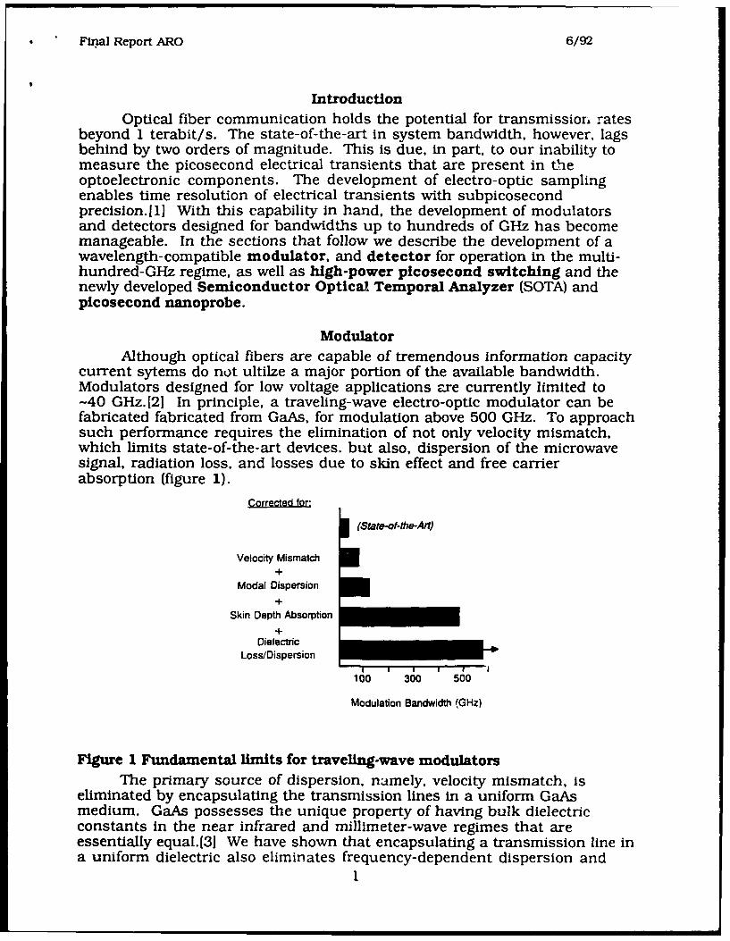
Although optical fibers are capable of tremendous information capacitycurrent sytems do not ultilze a major portion of the available bandwidth.Modulators designed for low voltage applications are currently limited to-40 GHz.[2] In principle, a traveling-wave electro-optic modulator can befabricated fabricated from GaAs, for modulation above 500 GHz. To approachsuch performance requires the elimination of not only velocity mismatch,which limits state-of-the-art devices, but also, dispersion of the microwavesignal, radiation loss, and losses due to skin effect and free carrierabsorption (figure 1).
(State-of-the-Art)
Velocity Mismatch
Modal Dispersion.+
Skin Depth Absorption
DielectricLoss/Dispersion
100 300 500
Modulation Bandwidth (GHz)
Figure 1 Fundamental limits for traveling-wave modulators
The primary source of dispersion, namely, velocity mismatch, iseliminated by encapsulating the transmission lines in a uniform GaAsmedium. GaAs possesses the unique property of having bulk dielectricconstants in the near infrared and millimeter-wave regimes that areessentially equal.J31 We have shown that encapsulating a transmission line ina uniform dielectric also eliminates frequency-dependent dispersion and
1
Final Report ARO 6/92
radiation losses otherwise present due to dielectric mismatch.Furthermore, losses associated with skin effect, and free-carrier absorptionhave been mitigated by lowering temperature.
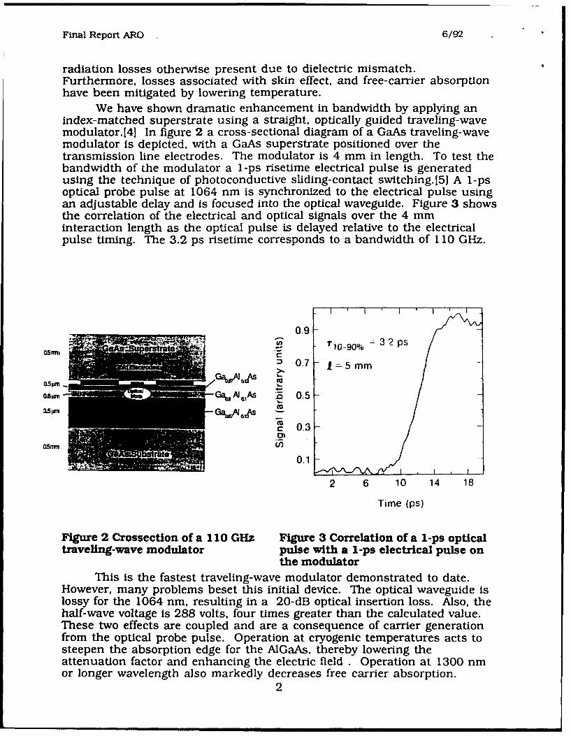
We have shown dramatic enhancement in bandwidth by applying anindex-matched superstrate using a straight, optically guided traveling-wavemodulator.[4] In figure 2 a cross-sectional diagram of a GaAs traveling-wavemodulator is depicted, with a GaAs superstrate positioned over thetransmission line electrodes. The modulator is 4 mm in length. To test thebandwidth of the modulator a 1-ps risetime electrical pulse is generatedusing the technique of photoconductive sliding-contact switching.[5] A 1-psoptical probe pulse at 1064 nm is synchronized to the electrical pulse usingan adjustable delay and is focused into the optical waveguide. Figure 3 showsthe correlation of the electrical and optical signals over the 4 mminteraction length as the optical pulse is delayed relative to the electricalpulse timing. The 3.2 ps risetime corresponds to a bandwidth of 110 GHz.
0.9i 1°-90° -• 3 2 ps
Sc 0.30fm C0.1
2 6 10 14 18
Time (ps)
Figure 2 Crossection of a 110 GHz Figure 3 Correlation of a 1-ps opticaltraveling-wave modulator pulse with a 1-ps electrical pulse on
the modulatorThis is the fastest traveling-wave modulator demonstrated to date.
However, many problems beset this initial device. The optical waveguide islossy for the 1064 nm, resulting in a 20-dB optical insertion loss. Also, thehalf-wave voltage is 288 volts, four times greater than the calculated value.These two effects are coupled and are a consequence of carrier generationfrom the optical probe pulse. Operation at cryogenic temperatures acts tosteepen the absorption edge for the AIGaAs, thereby lowering theattenuation factor and enhancing the electric field . Operation at 1300 nmor longer wavelength also markedly decreases free carrier absorption.
2
Final Report ARO 6/92
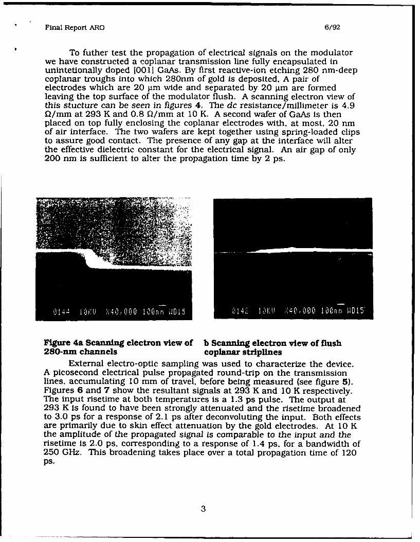
To futher test the propagation of electrical signals on the modulatorwe have constructed a coplanar transmission line fully encapsulated inunintetionally doped [0011 GaAs. By first reactive-ion etching 280 nm-deepcoplanar troughs into which 280nm of gold is deposited, A pair ofelectrodes which are 20 gim wide and separated by 20 g.m are formedleaving the top surface of the modulator flush. A scanning electron view ofthis stucture can be seen in figures 4. The dc resistance/millimeter is 4.9f2/mm at 293 K and 0.8 Q2/mm at 10 K. A second wafer of GaAs is thenplaced on top fully enclosing the coplanar electrodes with, at most. 20 nmof air interface. The two wafers are kept together using spring-loaded clipsto assure good contact. The presence of any gap at the interface will alterthe effective dielectric constant for the electrical signal. An air gap of only200 nm is sufficient to alter the propagation time by 2 ps.
Figure 4a Scanning electron view of b Scanning electron view of flush280-nm channels coplanar striplines
External electro-optic sampling was used to characterize the device.A picosecond electrical pulse propagated round-trip on the transmissionlines, accumulating 10 mm of travel, before being measured (see figure 5).Figures 6 and 7 show the resultant signals at 293 K and 10 K respectively.The input risetime at both temperatures is a 1.3 ps pulse. The output at293 K is found to have been strongly attenuated and the risetime broadenedto 3.0 ps for a response of 2.1 ps after deconvoluting the input. Both effectsare primarily due to skin effect attenuation by the gold electrodes. At 10 Kthe amplitude of the propagated signal is comparable to the input and therisetime is 2.0 ps, corresponding to a response of 1.4 ps, for a bandwidth of250 GHz. This broadening takes place over a total propagation time of 120ps.
3
S .. . .................... .. ~ m
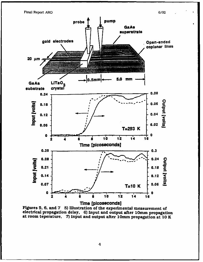
Final Report ARO 6/92
probe pumpGaAs
superstrate
gold electrodes Open-ended
coplanar lines
GaAs LITaO 3 i.0 mm
substrate crystal
0.24 - .0.08
-_ 0
,~0.18 0.06
a. I C
- 0.06 0.02 .TT ==2 993 KK
0* - -• -l " ' '-• " , • , • _ • i • • 0
4 6 8 10 12 14 16
Time [picoseconds]0.35 - 0.3
0.28 .2C0e0.21 , 0.18 2
= 0.14 0.12 1Ca.=2.
0.07 . T=10 K 0.06 &
0 02 8 10 1'2 1'4 16
Time [pfcoseconds]Figures 5, 6, and 7 5) T1lustration of the experimental measurement of
electrical propagation delay, 6) Input and output after 10mm propagation
at room teperature, 7) Input and output after 10mm propagation at 10 K
4
Final Report ARO 6/92
A careful determination of the propagation time was made bymeasuring the optical path difference between optical pulses synchronizedwith the arrival of the input and output signals. By knowing the propagationtime and the length of the superstrate an accurate measurement of theeffective dielectric constant can be determined. The effective dielectricconstant was found to be 11.60 (+/- 0.02). This value agrees remarkablywell with the bulk value of GaAs at 1.3 4m, 11.62 [3]. The difference inarrival times between electrical and optical pulses propagating in thisstructure would amount to -500 fs for a 10 mm interaction length.
The results are qualitatively revealing. The use of a mechanically-applied GaAs superstrate has served to demonstrate the feasibility of velocitymatching for ultrafast travelling-wave optoelectronic modulators. Practicaluse of this technique is being realized by regrowing GaAs over the substrateforming a superstrate that is an integral part of the device. Regrowthtechniques are now being investigated for compatibility with variouselectrode structures and compositions.
Detector
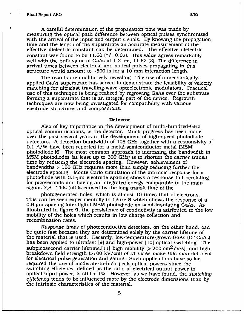
Also of key importance in the development of multi-hundred-GHzoptical communications, is the detector. Much progress has been madeover the past several years in the development of high-speed photodiodedetectors. A detection bandwidth of 105 GHz together with a responsivity of0.1 A/W have been reported for a metal-semiconductor-metal (MSM)photodiode.[61 The most common approach to increasing the bandwidth inMSM photodiodes (at least up to 100 GHz) Is to shorten the carrier transittime by reducing the electrode spacing. However, achievement ofbandwidths > 100 GHz requires more than simply reducing further theelectrode spacing. Monte Carlo simulation of the intrinsic response for aphotodiode with 0.1-gim electrode spacing shows a response tail persistingfor picoseconds and having an integrated energy comparable to the mainsignal.[7,81 This tail is caused by the long transit time of the
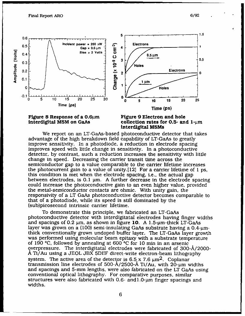
photogenerated holes, which is almost 10 times that of electrons.This can be seen experimentally in figure 8 which shows the response of a0.6 gm spacing interdigital MSM photodiode on semi-insulating GaAs. Asillustrated in figure 9, the persistence of conductivity is attributed to the lowmobility of the holes which results in low charge collection andrecombination rates.
Response times of photoconductive detectors, on the other hand, canbe quite fast because they are determined solely by the carrier lifetime ofthe material that is used. Recently, low-temperature-grown GaAs (LT-GaAs)has been applied to ultrafast [9] and high-power [10] optical switching. Thesubpicosecond carrier lifetime,[ 11] high mobility (> 200 cm 2 /V-s), and highbreakdown field strength (>100 kV/cm) of LT GaAs make this material idealfor electrical pulse generation and gating. Such applications have so farrequired the use of moderate-to-high peak optical powers since theswitching efficiency, defined as the ratio of electrical output power tooptical input power, is still < 1%. However, as we have found, the switchingefficiency tends to be influenced more by the electrode dimensions than bythe Intrinsic characteristics of the material.
5
Final Report ARO 6/92
5 1.5
0.6 fIncident power = 200 AW • Electrons
0.5 Gap = 0.6 11m E 4•' 0. 4 \Bias = 2 Volts
> 0.5"0.3 ,A 3
M H •oles
0.2 2 Electrons
E 0.1 o~~~ Pm1/ oe
-0.1 ... . I . . I . . . . I. . . .0 •0 5 10 15 20 25 30 5 10 15 20 25
Time [psi Time (ps)
Figure 8 Response of a 0.6%=m Figure 9 Electron and holeinterdigital MSM on GaAs collection rates for 0.5- and 1-jm
interdigital MSMs
We report on an LT-GaAs-based photoconductive detector that takesadvantage of the high breakdown field capability of LT-GaAs to greatlyimprove sensitivity. In a photodiode, a reduction in electrode spacingimproves speed with little change in sensitivity. In a photoconductivedetector, by contrast, such a reduction increases the sensitivity with littlechange in speed. Decreasing the carrier transit time across thesemiconductor gap to a value comparable to the carrier lifetime increasesthe photocurrent gain to a value of unity.[12] For a carrier lifetime of 1 ps,this condition is met when the electrode spacing, i.e., the actual gapbetween electrodes, is 0.1 gim. A further decrease in the electrode spacingcould increase the photoconductive gain to an even higher value, providedthe metal-semiconductor contacts are ohmic. With unity gain, theresponsivity of a LT GaAs photoconductive detector becomes comparable tothat of a photodiode, while its speed is still dominated by the(sub)picosecond intrinsic carrier lifetime.
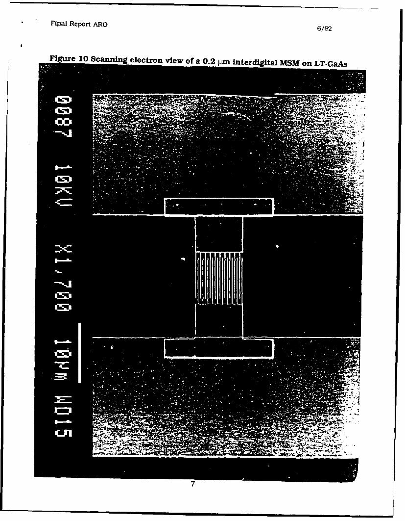
To demonstrate this principle, we fabricated an LT-GaAsphotoconductive detector with interdigitatal electrodes having finger widthsand spacings of 0.2 gim, as shown in figure 10. A 1.5-jim-thick LT-GaAslayer was grown on a (100) semi-insulating GaAs substrate having a 0.4-jim-thick conventionally grown undoped buffer layer. The LT-GaAs layer growthwas performed using molecular beam epitaxy with a substrate temperatureof 190 1C, followed by annealing at 600 0C for 10 min in an arsenicoverpressure. The interdigitatal electrodes were fabricated of 300-A/2000-A Ti/Au using a JEOL JBX 5DIIF direct-write electron-beam lithographysystem. The active area of the detector is 6.5 x 7.6 jim2 . Coplanartransmission line electrodes of 500-A/2500-A Ti/Au, with 20-jim widthsand spacings and 5-mm lengths, were also fabricated on the LT GaAs usingconventional optical lithography. For comparative purposes. similarstructures were also fabricated with 0.6- andl.0-jim finger spacings andwidths.
6
* inl eprt.0/9
Fiue1 cncoeetrnve fa02unltedgtlM Mo TG~
Final Report ARO 6/92
Referring to figure 10, the LT-GaAs photoconductive detector wasplaced between coplanar transmission lines (Zo = 90 0-) to assure goodcoupling of the generated electrical pulse to the propagating mode and alsoto eliminate parasitic losses. The detector was not antireflection (AR)coated in this initial work. A reference transmission line of identicaldimensions, but without the interdigitatal detector, was also fabricated onthe wafer to determine the system response. The technique of sliding-contact switching. which provides electrical excitation between the lineswithout the interdigitatal detector, can have a response < 0.5 ps.[5] Thephotoconductive detectors were characterized using the technique ofexternal electrooptic (EO) sampling [1]. A balanced, colliding-pulse, mode-locked dye laser operating at 610 nm with a repetition rate of 100 MH:: wasused, to producel50-fs pump and probe pulses. Electrical signals weremeasured on the transmission line at a distance of 450 gim from thedetector. Although not shown in the figure, the EO sampling crystalspanned both the detector/transmission-line as-embly and the referencetransmission line, so that the translation of the pump and probe beamsrequired to make either measurement was only - 200 jim.
A bias of 10 V dc was applied to the detector before breakdownoccurred, corresponding to a breakdown field strength of 500 kV/cm. Thisvalue is more than twice the highest that has been reported for LT GaAsunder dc-bias conditions, which was obtained using 20-jim-spacedelectrodes. [9] Our result represents the better measurement of the actualbreakdown field strength for LT-GaAs, since our 0.2-jim electrode spacingconfines the electric field to the 1.5-jim-thick LT GaAs epilayer. The darkcurrent for 1 V applied to the detector is 100 DA. At 8 V (400 kV/cm),where we chose to operate, the dark current increased to 300 nA. For anaverage optical power of 4 giW. the responsivity is 0.1 A/W. Past work using20-gm-spaced electrodes on LT-GaAs attained a responsivity of only 10-3A/W.[131 The 100-fold reduction in gap dimension therefore improves theresponsivity 100 fold. The value of 0.1 A/W is comparable to that for theresponsivity of high-speed photodiodes. The reflective losses at the surfacefrom the interdigitated electrodes and the semiconductor amounted to 70%of the incident signal, for an internal quantum efficiency of 68%.
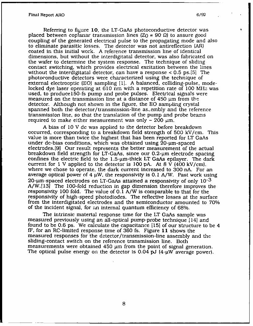
The intrinsic material response time for the LT GaAs sample wasmeasured previously using an all-optical pump-probe technique [141 andfound to be 0.6 ps. We calculate the capacitance [151 of our structure to be 4fF, for an RC-limited response time of 360 fs. Figure 11 shows themeasured responses for the detector/transmission-line assembly and thesliding-contact switch on the reference transmission line. Bothmeasurements were obtained 450 gm from the point of signal generation.The optical pulse energy on the detector is 0.04 pJ (4-jiW average power).
8
Final Report ARO 6/92
1.2.
FWHM=I.2pa1 IUW(dUB)=3750MH1
= 0.8 -.2 ,,° detect- M -- C ontenLR0.1A/W -
E 0.6a -2
V0 20 unsi~din 0o 0.4 V ,,Ncontact switch -
0.2 A=O.001AMW
"0.2 -4
z 0 N. .5
-0.2 .6 . .
0 2 4 6 8 10 100 200 300 400 500 600
Time [ps] FtiUqIcy (OHZI
Figure 11 Temporal response of Figure 12 The -3-dB point forthe photoconductive detector both signals occurs at 375and sliding-contact switch GHz.measured 450 gm from thepoint of signal generation.
102 , ... 100
: Gap -02 untV 0.8 ain.Iv 10' A 10,1 7
E 0.60 A E100 1-02
C CcS0.4 10-310.1 0"= IE A aaZ 0.2 1- 1o.2. o5z 10
00 2 4 6 a 10 1. .. ... 10.s0.01 0.1 1 1o 100
TIM pi En lgy/Pulso (MJl
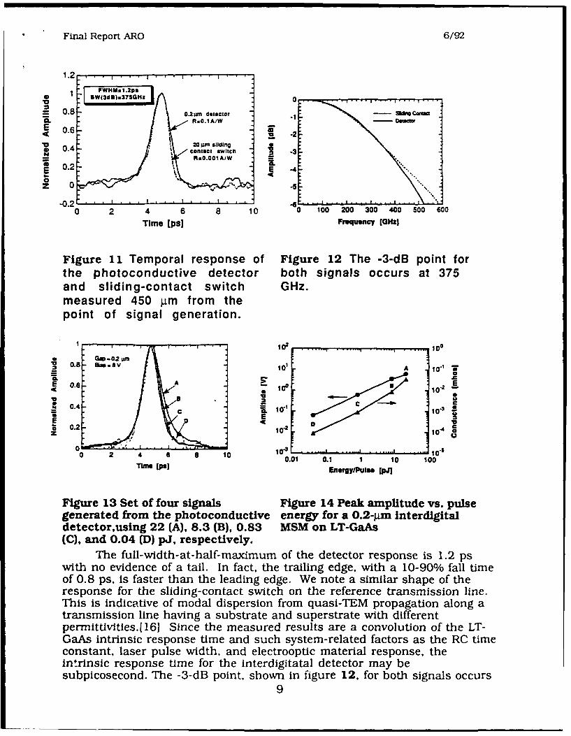
Figure 13 Set of four signals Figure 14 Peak amplitude vs. pulsegenerated from the photoconductive energy for a 0.2-gm interdigitaldetectorusing 22 (A), 8.3 (B), 0.83 MSM on LT-GaAs(C), and 0.04 (D) pJ, respectively.
The full-width-at-half-maximum of the detector response is 1.2 pswith no evidence of a tail. In fact, the trailing edge, with a 10-90% fall timeof 0.8 ps, is faster than the leading edge. We note a similar shape of theresponse for the sliding-contact switch on the reference transmission line.This is indicative of modal dispersion from quasi-TEM propagation along atransmission line having a substrate and superstrate with differentpermittivities.[161 Since the measured results are a convolution of the LT-GaAs intrinsic response time and such system-related factors as the RC timeconstant, laser pulse width, and electrooptic material response, theintrinsic response time for the interdigitatal detector may besubpicosecond. The -3-dB point, shown in figure 12. for both signals occurs
9
Final Report ARO 6/92
at 375 GHz, measured by taking their discrete Fourier transforms. A set ofwaveforms for several values of pulse energy is shown in figure 13. The foursignals have peak amplitudes of 0.06, 0.6, 3.5, and 6 V generated using0.04, 0.83, 8.3, and 22 pJ/pulse respectively. Figure 14 shows the peakamplitude and conductivity of these signals plotted against optical pulseenergy. We see that a nearly 500-fold increase in intensity expands theresponse only slightly from 1.2 to 1.5 ps. Under similar experimentalconditions, a high-speed photodiode would suffer significant temporalbroadening from space charge [1 7] and from low-frequency gain byphotoinduced band bending.[18] Thus, the LT-GaAs photoconductivedetector avoids the usual restriction of photodiodes to pulse energies below0.1 pJ.
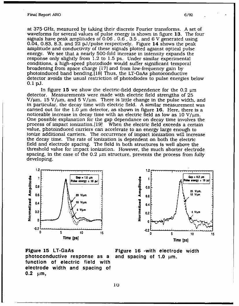
In figure 15 we show the electric-field dependence for the 0.2 pgmdetector. Measurements were made with electric field strengths of 25V/pgm, 15 V/gm, and 5 V/ptm. There is little change in the pulse width, andin particular, the decay time with electric field. A similar measurement wascarried out for the 1.0 pgm detector, as shown in figure 16. Here, there is anoticeable increase in decay time with an electric field as low as 10 V/pgm.One possible explanation for the gap dependance on decay time involves theprocess of impact ionization.[191 When the electric field exceeds a certainvalue, photoinduced carriers can accelerate to an energy large enough toionize additional carriers. The occurrence of impact ionization will increasethe decay time. The rate of ionization is dependent on both the electricfield and electrode spacing. The field in both structures is well above thethreshold value for impact ionization. However, the much shorter electrodespacing, in the case of the 0.2 pm structure, prevents the process from fullydeveloping.
1.2......... .. ......... I ......... 1.2 ...........................
. 1 Gap. 1.0 Gap = 0.2 pmPu., neVgyol pJ
~0.8 ~0.82 E 25VIPzM,
C 0.6 20 V/Izm < 0.6 15 V/Ii
0.4 .. - Pd 0.4 ,
vi
E0 . E 0.2 5 WP~M01 0Z 0 Z 0
"-0 .2 ... ..."0 .2 . . . . . . . . . '0 s 10 is 0 5 10 15
Time [psi Time [ps]
Figure 15 LT-GaAs Figure 16 -with electrode widthphotoconductive response as a and spacing of 1.0 grm.function of electric field withelectrode width and spacing of0.2 g~m,
'U
* Final Report ARO 6/92
In short, we have developed a new MSM-type photoconductivedetector, based on low-temperature-grown GaAs. fabricated using 0.2-gm-spaced interdigitatal electrodes. The response time measured directly byEO sampling, i.e., without deconvolution, is 1.2 ps. With no AR coating onthe detector, the responsivity is 0.1 A/W. To our knowledge, this is thefastest high-sensitivity photoconductive detector of any kind reported todate. In addition, it can be driven to an on-state resistance of 30 Q withlittle degradation in speed. This versatility permits the device to functionboth as a detector and a switch. In the switching mode, the device canperform either as a high-contrast gate with a picosecond window or as anefficient picosecond electrical-pulse generator. Such unique dualfunctionality together with ease of integration will permit a number ofdetector elements to be combined for acquiring and processing single-picosecond optical and electrical events with high efficiency and minimaltemporal distortion.
High-Power SwitchingThe unique properties of the LT-GaAs material which make it so
attractive for high-speed MSM photoconductors also give the material adistinct advantage in other applications which push the limits of speed, fieldbreakdown potential and dark resistivity. In order to further explore theutility of these epi-layers we have conducted a study of photocunductiveswitching at the kilovolt level with peak currents aproaching 20 Amps.
In recent years many applications have emerged for high-voltage,high-speed switching. The best technique now available for achievingkilovolt electrical pulses with picosecond risetimes is laser-drivenphotoconductive switching. To date, generation of a 1 kV pulse withrisetime and pulsewidth of 12 ps and 70 ps, respectively has been reported[20). This was accomplished using a high-resistivity semiconductor with a1.5 mm switch gap. The fastest risetime that is possible for this switchingstructure can be determined by calculating the propagation time over adistance equal to the switching gap. For this size gap a risetime of -12 ps isfound. Using electrodes separated by 10 gm, subpicosecond durationelectrical pulses with amplitudes up to 6 volts have also been laser-generated [13]. The competing needs of having a large photoconductivegap to hold off high voltage and a small gap to maintain high speed havehitherto left kilovolt amplitude and single picosecond pulse generationdecoupled.
With the advent of Low-Temperature Molecular-Beam-Epitaxy-grownGaAs (LT-GaAs) it is possible to fabricate extremely high resistivity, highbreakdown threshold switches. Now, dc electric fields in excess of 10 5V/cm are routinely achieved. It is also possible to take advantage of thefinite time necessary for thermal runaway or impact ionization to evolve bypulse-biasing the switching element for times shorter than breakdown [1].Using LT-GaAs and the technique of pulse biasing we have applied up to 1.3kV to a 100 gm gap. With this gap dimension, switching of the kilovolt-biasrequires less than 1 pJ of optical energy, obtainable with an amplifiedsubpicosecond dye laser.
11
Final Report ARO 6/92
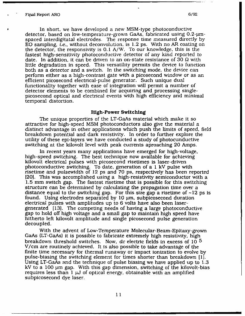
80-ps 80-WJ 1504s 900-nJ532-nm 620-nmn
~up to 1.3-kv\ / ~400-ps FWHM (
2-kV dc bias
Cr:GaAs Substrate LT-GaAs Substrate
Figure 17 HIgh p.'•wer switching experimental set-upA sche•atic diagram of the experimental configuration is shown in
figure 17 Our laser generates 150 fs, 2 pJ pulses at 620 nm with a 2-kHzrepetition rate, using a two-stage dye amplifier pumped by a frequencydoubleci Nd:YAG regenerative amplifier.[21, 22] Part of the frequency-doubled Nd:YAG regenerative amplifier output is used to excite a dc-biased4-mm-long semi-insulating-GaAs switch which is used as the pulse-biasnetwork. The switch is mounted in a microstrip line geometry between a-10 0 charge line and a 90 02 transmission line. Illuminated by an 80 AJ, 80ps optical pulse at 532 nm, this device produces an electrical pulse whichhas an amplitude equal to 70% of the dc bias voltage (up to 2 kV) and aduration of 400 ps. This pulse then biases a 90 Q coplanar stripline (100gim wide gold conductors separated by 100 gim) on a LT-GaAs substrate. Asthe bias pulse propagates along the transmission lines, a 150 fs,submicrojoule optical pulse excites the area between the lines. The highdensity of carriers formed within the LT-GaAs acts to short the electrodes.This form of sliding contact switching, in principle, allows total switching ofthe applied bias voltage [5]. External electro-optic sampling [1] in a LiTaO 3
crystal with a 150 fs pulse is used to measure the signal 300 grm from theswitch site. In our configuration the crystal has a half-wave voltage of -4 kVinsuring a response linear within 2% over the range of voltages measured.The calibration error of the measurement is estimated to be +/- 5% owingmainly to laser intensity fluctuations. Waveforms are recorded for differentsettings of bias voltage and ontical energy.
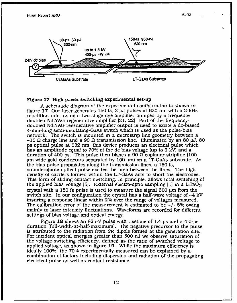
Figure 18 shows an 825-V pulse with risetime of 1.4 ps and a 4.0-psduration (full-width-at-half-maximum). The negative precursor to the pulseis attributed to the radiation from the dipole formed at the generation site.For incident optical energies greater than 500 nj we observe saturation ofthe voltage-switching efficiency. defined as the ratio of switched voltage toapplied voltage, as shown in figure 19. While the maximum efficiency isIdeally 100%, the 70% experimentally measured can be explained by acombination of factors including dispersion and radiation of the propagatingelectrical pulse as well as contact resistance.
12
Final Report ARO 6/92
1000 100 i
80080
.o 606000
>,6*v400S
~*200 40
0 20
-20011P I I I I I I I0i2e (ps) 0 200 400 600 800 1000Optical Energy (nJ)
Figure 18 825 V pulse switched on Figure 19 Switching efficiency100-ptm coplanar transmission lines (voltage switched/voltage biased) vs.on LT-GaAs optical energyThe rise time is ultimately limited by the 100-gm transmission linedimensions, however we also find a clear dependence on the carrier density.As illustrated in figure 4, we observe a degradation from 1. I ps to 1.5 psover the range of optical energy from 100 to 900 nJ. This corresponds to asaturation in the slew rate. The rise time nevertheless appears to beIndependent of the electric field (figure 5). The relation of the risetime to
the carrier density is still not well understood. Explanations involvingsaturation of the current density and strong carrier scattering are presentlybeing investigated.
13
Final Report ARO 6/92
1 .2 4 1 1 1 a gI I*~ 1 - 0 n 1.2 31 1 1 1 111~ a l * B11
1 500n 1
0.8 100 080vo
0.6 ~10J 0.6~0.4 ~0.4
OF 0.20.2 z z0 I0
-0.2 a -0.2 a I I I0 2 4 6 8 10 0 2 4 6 8 10
time (ps) time (Ps)
Figure2O Switch response for Figure 21 Switch response fordifferent optical pulse energies different applied voltages
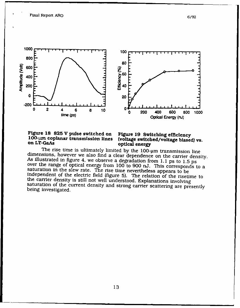
Although a subpicosecond recombination-time was anticipated fromprevious work [131, our measurements reveal a much longer recovery time.The tail was also found to increase when either the carrier density orapplied electric field were increased (figures 20 and 21). Significant localheating due to the extremely high current densities (up to 107 A/cm2 )drawn through the switch area may result in generation of additionalcarriers and explain the long recovery time.
Another possible explanation for the long recombination time involvesintervalley scattering which is known to be strongly dependent on bothelectric field and carrier density. The switched electric pulse shape reflectsthe evolution of the current density which is proportional to the product ofcarrier density and average carrier velocity. In GaAs, a photogenerated hotelectron under the influence of a strong electric field can scatter from thecentral valley to the high-effective-mass satellite X- and L-valleys therebyreducing its velocity and ability to produce current.
The scattering probability increases with the electrical field and,under our experimental conditions, we estimate that more than 80% of thecarriers scatter into the satellite valleys within 100 fs [231. The transfer ofthose electrons back into the central valley can take several picoseconds[241. As the pump energy increases so does the carrier density in thecentral valley. Consequently. the probability for an electron to scatter backinto the central valley decreases. As the carriers in the central valley beginto recombine (within a few hundred femtoseconds for LT-GaAs), theprobability of carrier transfer from the satellite valleys back to the centralvalley increases. The satellite valleys can then be seen as sources reinjectinghot electrons into the central valley at a rate dependent on the relativecarrier populations which are function of optical fluence, electric field andwavelength. This process will cause current to persist until all carriers
14
Final Report ARO 6/92
transfer back to the central valley where they either are trapped orrecombine.
In conclusion, we report on the application of LT-grown GaAs forphotoconductive switching using a pulse bias technique leading to thegeneration of a 825 V pulse with 1.4 ps rise time and duration of 4.0 ps.This represents the highest voltage ever obtained on the single picosecondtime scale. This new capability to produce ultrashort high peak powerelectrical pulses is of interest for applications in fields such as nonlinearmillimeter-wave spectroscopy, radar, high-energy physics and ultrafastInstrumentation.
Semiconductor Optical Temporal AnalyzerAt far lower power levels high-speed, high-sensitivity photodetectors
have been studied in other groups using the technique of picosecondphotoconductive sampling.[251 Although the emphasis has been placed onthe characterization of the detector,126, 27] the combination of high-speeddetector and sampling photogate can also be viewed as a high-speed opticalcorrelator. To our knowledge. this configuration has not yet been applied tothe measurement of optical waveforms. This is due, in part, to the relativelyslow detectors that have been available. However, to have tue highest speedand sensitivity requires more than simply a fast detector. Both thephotodetector and photo-gate must have high speed combined with highsensitivity.
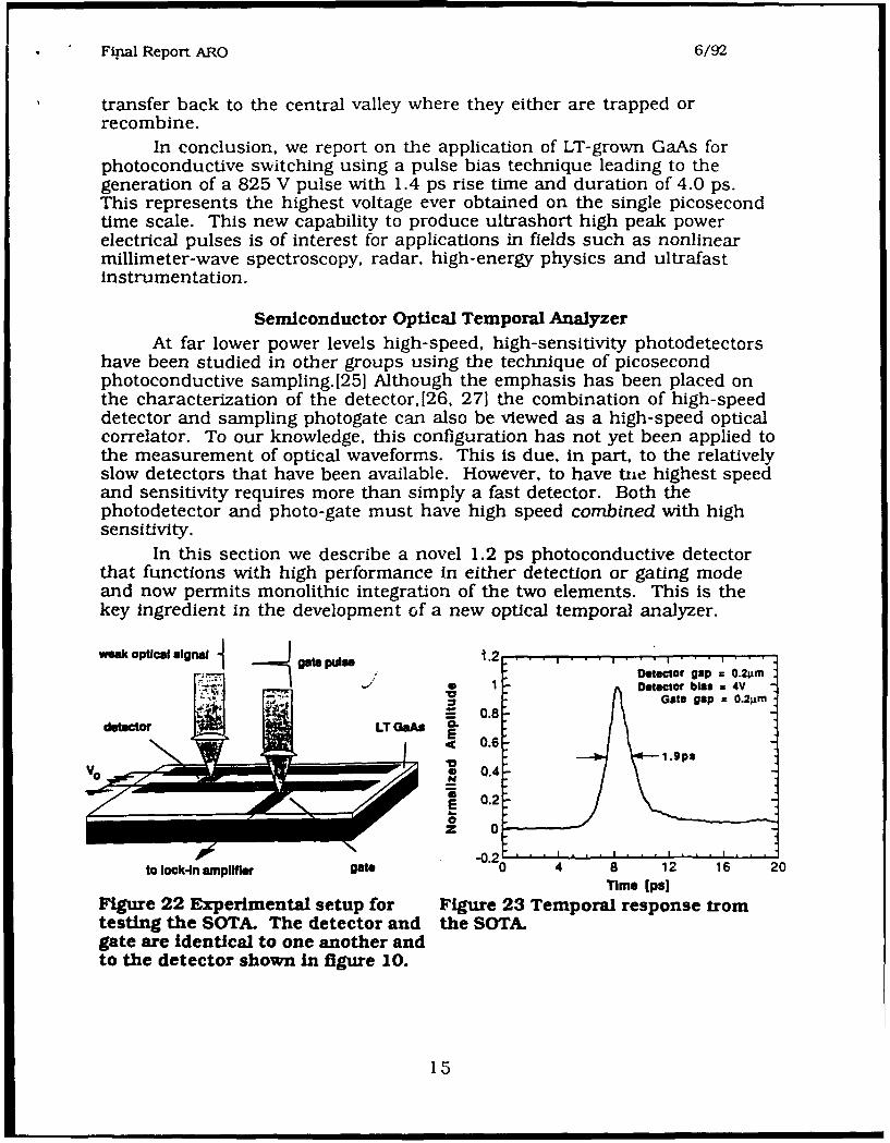
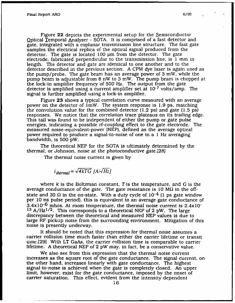
In this section we describe a novel 1.2 ps photoconductive detectorthat functions with high performance in either detection or gating modeand now permits monolithic integration of the two elements. This is thekey ingredient in the development of a new optical temporal analyzer.
wreak optical signal gatePulse t.2................Detector gap = O.2gmDetector bias = 4V
Gote gap c O.2gimdetector LT Ga• C
EQ( 0.6
VMW V l.ps0 0.4
E0.2Sib . ,
z 0
to lock4n ampllfer gate -0.20 4 8 12 16 20"Time (ps]
Figure 22 Experimental setup for Figure 23 Temporal response fromtesting the SOTA. The detector and the SOTA.gate are Identical to one another andto the detector shown in figure 10.
15
Final Report ARO 6/92
Figure 22 depicts the experimental setup for the SemiconductorQptical Temporal Analyzer - SOTA. It is comprised of a fast detector andgate, integrated with a coplanar transmission line structure. The fast gatesamples the electrical replica of the optical signal produced from thedetector. The gate is located 100 gim from the detector. The gateelectrode, fabricated perpendicular to the transmission line, is 1 mm inlength. The detector and gate are identical to one another and to thedetector described in the previous section. A CPM dye laser is again used asthe pump/probe. The gate beam has an average power of 3 mW, while thepump beam is adjustable from 8 nW to 3 mW. The pump beam is chopped atthe lock-in amplifier frequency of 500 Hz. The output from the gatedetector is amplified using a current amplifier set at 10-7 volts/amp. Thesignal is further amplified using a lock-in amplifier.
Figure 23 shows a typical correlation curve measured with an averagepower on the detector of 1mW. The system response is 1.9 ps, matchingthe convolution value for the combined detector (1.2 ps) and gate (1.5 ps)responses. We notice that the correlation trace plateaus on its trailing edge.This tail was found to be independent of either the pump or gate pulseenergies, indicating a possible rf-coupling effect to the gate electrode. Themeasured noise-equivalent-power (NEP), defined as the average opticalpower required to produce a signal-to-noise of one in a 1 Hz averagingbandwidth, is 500 pW.
The theoretical NEP for the SOTA is ultimately determined by thethermal, or Johnson, noise at the photoconductive gate. 1281
The thermal noise current is given by
ithermal= ý- V__ [A/H- zl
where k is the Boltzman constant, T is the temperature, and G is theaverage conductance of the gate. The gate resistance is 10 MfK in the off-state and 30 02 in the on-state. With a duty cycle of 10-4 (1 ps gate windowper 10 ns pulse period), this is equivalent to an average gate conductance of3.4x10"6 mhos. At room temperature, the thermal noise current is 2.4x10⁻¹³ A/Hzl/ 2 . This corresponds to a theoretical NEP of 2 pW. The largediscrepancy between the theoretical and measured NEP values is due tolarge RF pickup noise from the surrounding environment. Mitigation of thisnoise is presently underway.
It should be noted that this expression for thermal noise assumes acarrier collision time much faster than either the carrier lifetime or transittine.[291 With LT GaAs. the carrier collision time is comparable to carrierlifetime. A theoretical NEP of 2 pW may, in fact, be a conservative value.
We also see from this expression that the thermal noise currentincreases as the square root of the gate conductance. The signal current, onthe other hand, increases linearly with gate conductance. The highestsignal-to-noise Is achieved when the gate is completely closed. An upperlimit, however, exist for the gate conductance, imposed by the onset ofcarrier saturation. This effect, evident from the intensity-dependent
16
Final Report ARO 6/92
temporal broadening seen in figure 5. already degrades our system responseby 10%.
In short, we have taken advantage of the features of the newlydeveloped MSM photoconductive detector on LT-GaAs to develop apicosecond resolution, semiconductor optical temporal analyzer (SOTA).The measured NEP for the system is 500 pW. The technique is jitter-free,permitting long integration times. Ultraweak picosecond fluorescence andscattering experiments, as well as other ultrafast phenomena can be time-resolved using this relatively simple tool.
Picosecond Nanoprobe
The continuing advances made in the development of semiconductordevices have pushed the speed of some devices to frequencies in excess of400 GHz [30]. To accurately test devices with this response requires thedevelopment of new probing techniques, capable of not only high temporaland spatial resolution, but also noninvasive inspection. Existing, purelyelectronic measurement instruments, such as vector network analyzers,spectrum analyzers, and sampling oscilloscopes, are not adequate tools fortesting state-of-the-art high-speed integrated circuits. The rf networkanalyzer, which is now gaining acceptance for use up to 100 GHz, still hasdifficulties with test-fixture transitions, de-embedding of parasiticparameters, and overall accuracy and convenience of operation.Furthermore, internal nodes cannot be tested at high speeds with the low-impedance probe technology that is now available for use with suchinstruments.
In contrast to purely electrical approaches, electro-opticmeasurement techniques have many unique features for high-speed circuittesting. The major attribute gained from this marriage of optics andelectronics is speed - both in temporal resolution, and in acquisition time.External-probe-electro-optic (EO) sampling has a temporal resolution as fastas 290-fs (>1 THz bandwidth) and offers the greatest flexibility of anyoptically-based technique now available.[1] External EO sampling uses asmall (50-jm 2 ) tip of electric-field sensitive material (LiTaO3 or LiNbO 3 ) tomake measurements of fringing electric fields that extend above the circuitunder test. In developing applications for this probe technology, extendingfrom high-speed, non-loading pin testing of packaged devices, todevelopment of a 100-GHz electro-optic network analyzer for testing ofhigh-speed discrete analog devices[31], we also encountered limitations inspatial resolution (-5 gm) and signal sensitivity (>10 mV/IHz). Also,absolute voltage measurements have been subject to interpretation.
We have recently developed a new optically-based external probe thatpromises to overcome these limitations while maintaining a temporalresolution of 1-ps. The probe concept is based on photoconductive (PC)sampling, which has the highest sensitivity of any optically-based samplingtechnique.J32] The probe we developed has a demonstrated sensitivity of 1.iV/qHz and is capable of measuring the absolute voltage of the device-under-test. The dynamic range is >106, making possible measurements from themicrovolt to the 10-volt level. The probe, though contacting in nature, isnon-invasive with a load resistance of > 100 kQ and a capacitance of <0. 1 F.It makes contact to the device under test using a conical-shaped tip which
17
Final Report ARO 6/92
will have a tip radius of < 100 nm. The sensitivity and speed of the probe areindependent of the tip-to-device contact resistance up to 10 kK2.
, 3 gim titanium
% % %2.3 jim photoresist
substrate
Figure 24 Scanning electron view of Figure 25 Process for forming thesubmicrometer tip formed by submicrometer tip.depositing titanium through a 3-tgmself-closing hole.
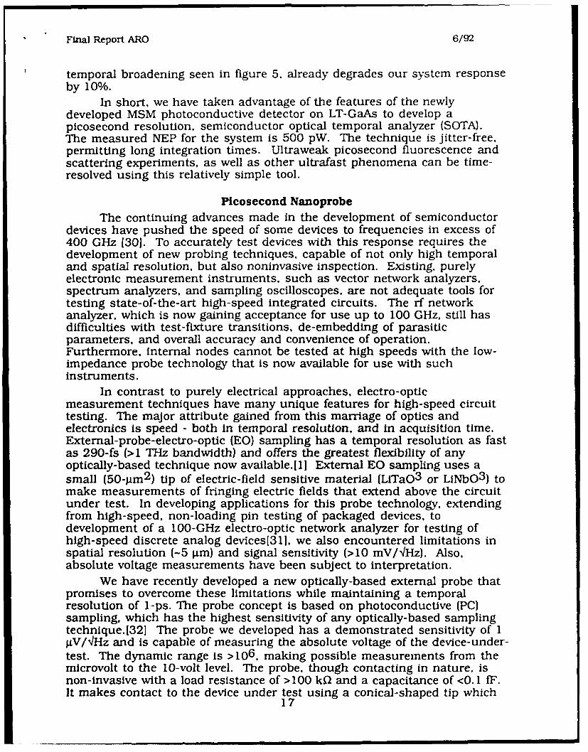
To make submicron spatial resolution possible in testing integratedcircuits, we have we have adapted the technology for forming ruggedmetallic cones from the field of vacuum microelectronics.[33, 34] Thisprocess employs conventional, repeatable photolithographic techniques toform tips with 100-nm-radius of curvature (figure 24). This is done asfollows: On a substrate suitable for photolithographic processing, a layer ofphoto-resist is hardened, patterned, and developed, leaving a 3-gm roundhole at the location where a tip is desired. Deposition of a few microns ofmetal, such as titanium, simultaneously causes the growth of a conical tip atthe base of this hole and the narrowing of its opening. This forms a sharp tipby virtue of the shrinking-aperture.
Subsequently, the thick metalization is removed by dissolving thephoto-resist layer, as shown in figure 25. The remaining structure is asharp, rugged tip at a precisely defined location on the substrate. Thisrecipe is compatible with a many other processes on GaAs and Si.
18
Final Report ARO 6/92
optical pulse
• .... .. . ,-.
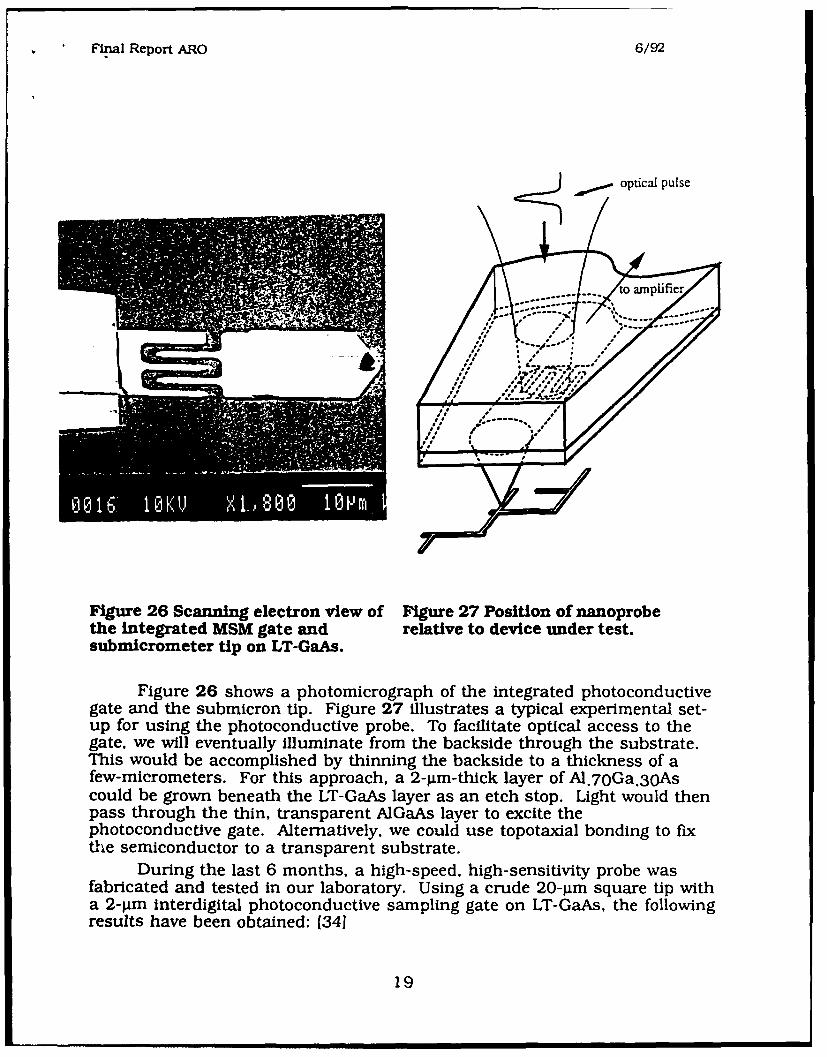
Figure 26 Scanning electron view of Figure 27 Position of nanoprobethe integrated MSM gate and relative to device under test.submicrometer tip on LT-GaAs.
Figure 26 shows a photomicrograph of the integrated photoconductivegate and the submicron tip. Figure 27 illustrates a typical experimental set-up for using the photoconductive probe. To facilitate optical access to thegate, we will eventually Illuminate from the backside through the substrate.This would be accomplished by thinning the backside to a thickness of afew-micrometers. For this approach, a 2-jim-thick layer of Al.70Ga.3OAscould be grown beneath the LT-GaAs layer as an etch stop. Light would thenpass through the thin, transparent AIGaAs layer to excite thephotoconductive gate. Alternatively, we could use topotaxial bonding to fixthe semiconductor to a transparent substrate.
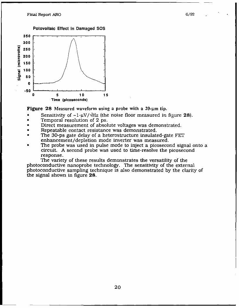
During the last 6 months, a high-speed, high-sensitivity probe wasfabricated and tested in our laboratory. Using a crude 20-1im square tip witha 2-jim interdigital photoconductive sampling gate on LT-GaAs, the followingresults have been obtained: (341
19
Final Report ARO 6/92
Potovoltaic Effect In Damaged SOS
350 ---
300U1= 2500p 200
150
;100
._ 50
0
-500 5 10 15
Time (picoseconds)
Figure 28 Measured waveform using a probe with a 20-4.m tip.* Sensitivity of -1-gtV/'/Hz (the noise floor measured in figure 28).• Temporal resolution of 2 ps.* Direct measurement of absolute voltages was demonstrated.0 Repeatable contact resistance was demonstrated.* The 30-ps gate delay of a heterostructure insulated-gate FET
enhancement/depletion mode inverter was measured.* The probe was used in pulse mode to inject a picosecond signal onto a
circuit. A second probe was used to time-resolve the picosecondresponse.The variety of these results demonstrates the versatility of the
photoconductive nanoprobe technology. The sensitivity of the externalphotoconductive sampling technique is also demonstrated by the clarity ofthe signal shown in figure 28.
20
Final Report ARO 6/92
Summary of ResultsThe work carried out under this contract has yield steady progress en
route to multi-hundred GHz optical communications. The conditions forvelocity matching and high fidelity signal transmission in an opticalmodulator have been met. A wavelength-compatable high-speedphotoconductive detector has been developed. Novel means of testing fastoptical transients has been dedveloped. A probe which has the potential totest devices and circuits in the multi-hudred GHz range has beendemonstrated. The key points of these results are outline below:
Modulator* Propagation speed of electrical signals matches optical signal speed to
within two parts in a thousand corresponding to <500-fs walk-off in10mm.
0 1.4 ps pulse response is preserved over 10 mm of propagation atcryogenic temperatures
* 2.1 ps pulse response is preserved over 10 mm of propagation at roomtemperature.
Detector* A wavelength-compatable MSM photoconductive detector based on
LT-GaAs is demonstrated to have a 375 GHz bandwidth (-3-dB point),0. 1 A/W responsivity, and functionality for picosecond detection andgating.
High Voltage Switching825 Volts is switched in LT-GaAs with a 1.4-ps rise time and a 4-pswidth in a 100-pLm-wide transmission line gap.
SOTA* An optical sampling structure based on the LT-GaAs MSM
photoconductive detector/gate is shown to have 1.9 ps resolution andpW sensitivity.
Picosecond NanoprobeA novel external circuit probe based on the MSM technology isdemonstated with 2.3 ps temporal resolution and absolute microvoltsensitivity.
21
Final Report ARO 6/92
References1. J. F. Whitaker, J. A. Valdmanis, M. Y. Frankel, S. Gupta. J. M. Chwalek.
and G. A. Mourou, Microelectron. Eng. 12, 369 (1990).2. S. K. Korothy, G. Eisenstein, R. S. Tucker, J. J. Veselka, and G. Raybon,
Appl. Phys. Lett., 50, 1631, (1987).3. E. D. Palik, Handbook of Optical Constants and Solids, Academic Press
Inc. 433, 1985.4. d. Nees, S. Williamson, and G. Mourou, Appl. Phys. Lett., 54, 1962,
(1989).5. D. R. Grischkowsky, M4. B. Ketchen, C-C. Chi, I. N. Duling III,
N. J. Halas, J-M. Halbout, IEEE J. Quantum Electron. 24, 221 (1988).6. J. Van Zeghbroek, W. Patrick, J-M. Halbout, and P. Vettiger, IEEE
Electron Device Lett. 9, 527 (1988).7. W. C. Koscielniak, J. L. Pelouard, and M. A. Littlejohn, Appl. Phys. Lett.
54, 567 (1989).8. W. C. Koscielniak, J. L. Pelouard, and M. A. Littlejohn, IEEE Photon.
Technol. Lett. 2. 125 (1990).9. F. W. Smith, H. Q. Le, V. Diadiuk, M. A. Hollis, A. R. Calawa, S. Gupta. M.
Frankel, D. R. Dykaar, G. A. Mourou, and T. Y. Hsiang, Appl. Phys. Lett.54, 890 (1989).
10. T. Motet, J. Nees, S. Williamson, and G. Mourou, Appl. Phys. Lett. 59,1455 (1991).
11. J. F. Whitaker, J. A. Valmanis, M. Y. Frankel, S. Gupta, J. M. Chwalek,and G. A. Mourou, Microelectron. Eng. 12, 369 (1990).
12. S. M. Sze, Physics of Semiconductor Devices, 2nd ed. (Wiley, NewYork, 1981), p. 746.
13. M. Y. Frankel, J. F. Whitaker, G. A. Mourou, F. W. Smith, A. R. Calawa,IEEE Trans. Electron Devices 37, 2493 (1990).
14. S. Gupta, J. Pamulatpati, J. Chwalek, P. K. Bhattacharya, and G. Mourou,in Ultrafast Phenomena VII, edited by C. B. Harris, E. P. Ippen, G. A.Mourou, and A. H. Zewail (Springer-Verlag, Berlin, 1990), p. 297.
15. J. B. D. Soole and H. Schumacher, IEEE Trans. Electron Devices 37,2285 (1990).
16. S. Gupta, J. F. Whitaker, and G. A. Mourou, IEEE Microwave GuidedWave Lett. 1, 161, (1991).
17. C. Moglestue, J. Rosenzweig, J. Kuhl, M. Klingenstein, M. Lambsdorff,A. Axmann, Jo. Schneider, and A Hulsmann, J. Appl. Phys. 70, 2435(1991).
18. D. L. Rogers,Picosecond Electronics and Optoelectronics II, edited byF. J. Leonberger, C. H. Lee. F. Capasso, and H. Morkog (Springer-Verlag, Berlin, 1987).
19. S. M. Sze, Physics of Semiconductor Devices, 2nd ed. (Wiley, NewYork, 1981), p. 45.
20. D. G. Steams, J. Appl. Phys., 65 (3), p. 1308 (1989).
22
"Final Report ARO 6/92
21. T. Norris, T. Sizer II, and G. Mourou, "Generation of 85 fs Pulses bySynchronous Pumping of a Colliding Pulse Mode-locked Dye Laser", J.Opt. Soc. Am. B. 2, April 1985.
22. I. N. Duling 111, T. Norris, T. Sizer II, P. Bado, and G. Mourou."Kilohertz Synchronouse Amplification of 85 fs Optical Pulses", J. Opt.Soc. Am. B, 2, April 1985.
23. G. lafrate, "High-Speed Transport in III-V Compounds", in GalliumArsenide Technology, edited by D. K. Ferry, SAMS 1985.
24. M. C. Nuss and D. H. Auston, "Direct Subpicosecond Measurements ofCarrier Mobility of Photoexcited Electrons in GaAs", in PicosecondElectronics and Optoelectronics II, edited by F. J. Leonberger,Springer-Verlag 1987.
25. D. H. Austin, Picosecond Optoelectronic Devices, edited by Chi H. Lee(Academic Press Inc., 1984), p. 73.
26. J. Van Zeghbroek, W. Patrick, J-M Halbout, --.A P. Vettiger, IEEETransactions on Electron Devices, 37, 2493 (1990).
27. M. Klingenstein, J. Kuhl, J. Rosenzweig C. Moglestue, A. Axmann,Applied Physics letters, 70, 243o, ( .9",1).
28. Martin van Exter, and Daniel 'Xiischkowsky, IEEE Transactions onMicrowave Theory -ind Teer- - 4ues, MTr-38, 1684 (1990).
29. R. H. Kingston, Dr .ection , ,tical and Infrared Radiation (Springer-Verlag, Berlin, - ' 8), p. 5!-.
30. P. Ho, M.Y. Kao, P.C. Chao, i..H.G. Duh, J.M. Ballingall, S.T. Allen, AXJ.Tess: er, P.M. Smith, Electron. Lett., 27, 325 (1991).
31. M.Y. Frankel, J.F. Whitaker, G.A. Mourou, and J.A. Valdmanis,"Ultrahigh-bandwidth vector network analyzer based on externalelectro-optic sampling," Solid-State Electronics, vol. 35, pp. 325-332(Mar. 1992).
32. C.H. Lee, "Picosecond optics and microwave technology," IEEE Trans.on Microwave Theory Tech., vol. 38, May 1990, pp. 596-607.
33. C. Spindt, I. Brodie, L. Humphrey, and E. Westerberg, "PhysicalProperties of Thin Film Field Emission Cathodes with MolybdenumCones," J. Appl. Phys., Vol. 37(12), December 1976.
34. J. Kim, S. Williamson, J. Nees, S. Wakana, "A Novel Free-StandingAbsolute-Voltage Probe With 2.3-Picosecond Resolution and 1-Microvolt Sensitivity," Ultrafast Phenomena VII, 8-12 June, 1992,Antibes-Juan-Lesp-Pins, France.
23
Papers published or presented
* 1.4 Picosecond-Risetime High-Voltage Photoconductive Switching, T. Motet, J. Nees, S.Williamson, and G. Mourou, Applied Physics Letters, 59, 1984, 1991.
0 375-GHz-Bandwidth Photoconductive Detector, Y. Chen, S. Williamson, T. Brock, F.W. Smith, and A. R. Calawa, Applied Physics Letters, 59, 1455, 1991.
0 S. Gupta, S. L. Williamson, Y. Chen, J. F. Whitaker, and F. W. Smith, UltrafastDetectors using II1-V Epilayers Grown by Molecular-Beam-Epitaxy at Low Temperatures,Laser Focus World, July 1992.
* 1.9 Picosecond Optical Temporal Analyzer using 1.2 Picosecond Photoconductor andGate, Y. Chen, S. L. Williamson, T. Brock, F. W. Smith, IEEE International ElectronDevice Meeting, Washington D.C., 417, 1991.
* Development of a Multi-Hundred Gigahertz Electro-Optic Modulator and Photodetector, S.Williamson, Y. Chen, D. Craig, and G. Mourou, Proc. DOD Fiber Optics '92, 271 1992.
• Picosecond High-Voltage Pulses Generated Using Low-Temperature GaAs, T. Motet, J.Nees, S. Williamson, and G. Mourou, Conf. of Materials Research Society, Boston 1991.
* Multi-Hundred Gigahertz Photodector Development Using LT GaAs, Y. Chen, S.Williamson, T. Brock, F. W. Smith, and A. R. Calawa, Conf. of Materials ResearchSociety, Boston, 1991.
* Efficient High Voltage Picosecond Photoconductive Switching, T. Motet, J. Nees, S.Williamson, and G. Mourou, at Picosecond Electronics and Optoelectronics IV in Salt LakeCity, March '91
* Propagation of Picosecond Electrical Pulses in GaAs for Velocity-Matched Modulators, Y.Chen, J. Nees, and S. Williamson, at Picosecond Electronics and Optoelectronics IV inSalt Lake City, March '91.
* Single-Picosecond High-Voltage Photoconductive Switching Using Low-Temperature-Grown GaAs, T. Motet, J. Nees, S. Williamson, and G. Mourou, at Conference on Laserand Electro-Optics in Baltimore, May '91.
* 1.2 ps High-Sensitivity Photodetector/Switch Based on Low-Temperature-Grown GaAs,Y. Chen, S. Williamson, and T. Brock, at Conference on Lasers and Electro-Optics inBaltimore, May '91.
Patent Applications
* l-Picosecond High-Sensitivity Photoconductor
Students Graduating
* Yi Chen, PhD in Electrical Engfineering, University of Michigan, May 1991
25