Embed Size (px)
Citation preview

ATLAS Project Document No: Page:1 of 451
ATL-IP-ES-0007 Rev. No.: 01
Requirements for Pixel Detector Services
ATLAS Project Document No: Institute Document No. Created: 17. 01. 2000 Page: 1 of 4543
ATL-IP-ES-0007 Modified: 28.02.01 Rev. No.: 1
Specification
Requirements for Pixel Detector Services
Abstract
This document provides an overview of the requirements for the pixel detector services. All the basic design and technological choices are discussed. Rules for numbering and identification are established. The document is the starting point for the detailed design of the services and represents the official pixel interface document for the integration of the Pixel detector services within the rest of ATLAS.
Prepared by: M. Olcese
K. Einsweiler E.Anderssen
M.Garcia-Sciveres W.Ockenfels
M.Oeferkamp
Checked by:
Approved by:

ATLAS Project Document No: Page:2 of 451
ATL-IP-ES-0007 Rev. No.: 01
Distribution List
History of Changes
Rev. No. Date Pages Description of changes
Table of Contents
1 INTRODUCTION ............................................................................................................................. 55 2 SCOPE OF THE DOCUMENT......................................................................................................... 55 3 LAYOUT, INSTALLATION AND OPERATION ISSUES.................................................................. 55
3.1 Detector layout............................................................................................................................................................. 55
3.2 Installation ................................................................................................................................................................... 66
3.3 Operating environment and barriers ........................................................................................................................ 66 3.3.1 Faraday cage requirements..................................................................................................................................... 77 3.3.2 Thermal/gas barrier requirements .......................................................................................................................... 77 3.3.3 Central support tube requirements ......................................................................................................................... 77 3.3.4 Forward support tube requirements........................................................................................................................ 88 3.3.5 End plug requirements ........................................................................................................................................... 88 3.3.6 Beam pipe requirements......................................................................................................................................... 99
3.4 Radiation levels............................................................................................................................................................ 99
4 OUTLINES OF PIXEL DETECTOR SERVICES ............................................................................ 109 5 MODULARITY AND GROUPING ................................................................................................ 1212 6 SERVICE ROUTING AND BREAK POINTS ............................................................................... 1313
6.1 Phi-layout ................................................................................................................................................................. 1414
7 DESIGN ISSUES......................................................................................................................... 1615
7.1 Design rules and standards..................................................................................................................................... 1615

ATLAS Project Document No: Page:3 of 451
ATL-IP-ES-0007 Rev. No.: 01
7.2 Local services ........................................................................................................................................................... 1615
7.2.1 Allowable voltage drops..................................................................................................................................... 1615 7.2.2 Module services ................................................................................................................................................. 1717
7.2.2.1 Module power cables and power budget....................................................................................................... 1717 7.2.2.2 Signal cables ................................................................................................................................................. 1817
7.2.3 Opto-board services............................................................................................................................................ 1918 7.2.3.1 Voltage supplies and power budget .............................................................................................................. 1918 7.2.3.2 Signal cables ................................................................................................................................................. 1918
7.2.4 Cable sizes.......................................................................................................................................................... 2019
7.3 Cooling system......................................................................................................................................................... 2221 7.3.1 Pressure drop budget and boundary conditions.................................................................................................. 2322 7.3.2 Sizing of cooling pipes....................................................................................................................................... 2423 7.3.3 Electrical services for the cooling system .......................................................................................................... 2524
7.4 Global services ......................................................................................................................................................... 2625 7.4.1 Active thermal shield ......................................................................................................................................... 2625 7.4.2 Environmental temperature control .................................................................................................................... 2625 7.4.3 Environmental gas system.................................................................................................................................. 2625
7.5 Grounding and shielding ........................................................................................................................................ 2726
8 SERVICE INTEGRATION............................................................................................................ 2827
8.1 From stave to PP0.................................................................................................................................................... 2827
8.2 Disk pigtails.............................................................................................................................................................. 2928
8.3 Pipe network in the frame volume ......................................................................................................................... 2928
8.4 PP0............................................................................................................................................................................ 3029
8.5 From PP0 to PP1 ..................................................................................................................................................... 3029
8.6 Multi-conductor cables ........................................................................................................................................... 3231
8.7 From PP1 to PP2 ..................................................................................................................................................... 3332
8.8 PP2............................................................................................................................................................................ 3533
8.9 From PP2 to PP3 ..................................................................................................................................................... 3735
8.10 PP3 ........................................................................................................................................................................ 3836
8.11 From PP3 to service cavern ................................................................................................................................ 3836
8.12 Inside the service cavern ..................................................................................................................................... 3836
9 IDENTIFICATION SCHEME ........................................................................................................ 3836
9.1 Introduction ............................................................................................................................................................. 3836
9.2 Barrel services ......................................................................................................................................................... 3937
9.3 Disk services............................................................................................................................................................. 4139
10 OVERALL SERVICE INVENTORY........................................................................................... 4240


ATLAS Project Document No: Page:5 of 451
ATL-IP-ES-0007 Rev. No.: 01
1 INTRODUCTION The pixel detector is a very compact and sophisticated system with a very high modularity. There is a very large collection of services connecting the pixel detector to the external acquisition and control systems. The design of the services is a very complex system issue involving interfaces with not only almost all the internal systems, but also with many external detectors. The service integration is a long iterative process evolving with the evolution of the design of the detector. It is therefore not very easy for those involved in the design of the services, to keep trace of all the continuos but physiological changes. The aim of this document is to establish a baseline for the major technological and design choices to be considered as a solid input aiming for a more effective co-ordination of the involved design groups within the pixel detector. The document is also aiming to provide all the required information to the Inner Detector Service Working Group in charge of the service integration for the Inner Detector. This information includes: • Cable sizes from PP1 outward • Pipe sizes from PP1 outward, insulation, grouping • Requirements for cooling (capacity) • PP2 requirements: envelopes, keep clear zones for access • Requirements for racks on service platforms Other detailed design issues will be addressed by specific documents.
2 SCOPE OF THE DOCUMENT The services of the pixel detector include all physical interfaces with the outside of ATLAS providing the required energy input and control signals for the operation of the detector and transferring the acquisition data to the external read out system. Strictly related to the services are the grounding and shielding issues whose requirements often have a significant impact on the design in some areas. For instance the electrical coupling/isolation between different structural components and their connection to ground. Due to this close relationship with service design the grounding and shielding issues are de facto discussed in this document.
3 LAYOUT, INSTALLATION AND OPERATION ISSUES
3.1 Detector layout The layout of the pixel system is described in detail in another document (ATL-IP-EP-0004), here we summarise the main features relevant for the services. The basic electronic unit of the pixel detector is the module. The pixel system is made of: • 3 barrel layers • 6 disks (3 per end) with the same geometry.

ATLAS Project Document No: Page : 6 of 451
ATL-IP-ES-0007 Rev. No.: 1.0
Each barrel layer consists of a turbine like sequence of tilted staves. The stave design is unique throughout the three layers. One stave supports and cools 13 electronic modules. There is one cooling tube per stave and two staves are cooled in series. The major geometrical parameters of the barrel layout are given in the following table:
Nom.radius (mm) No. of staves B-layer 50.5 22 Layer 1 88.5 38 Layer 2 122.5 52
Each disk consists of a sequence of 8 sectors, all with the same geometry. One sector supports and cools 6 modules, 3 on each face. All the modules are placed at the same radius. There is one cooling tube per sector and two sectors are cooled in series.
3.2 Installation The pixel detector system has been designed to be integrated inside the Inner Detector (ID) at the last stage of installation, when all other ID subdetectors are already in place. The pixel detector is installed from side C. For integration reasons the pixel detector is structurally split in two parts one external (two outer layers and all the 6 disks) and the innermost barrel layer (B-layer) installed independently. The B-layer diameter is too small to pass over the beampipe end-flanges, and hence it must be clam-shelled around the beampipe and inserted into the outer pixel assembly. For this reason the services of the outer part and of the B-layer follow a different routing. The two outer barrel layers and the disks are assembled together on surface, their services follow a common routing and they are almost evenly distributed between both sides: A and C. The B-layer services come out of the pixel area from side C only.
3.3 Operating environment and barriers The operating environment of the pixel detector is required to be: 1. cold (temperature ranging from 0°C to –10°C) to minimise the radiation damage of the pixel
sensors 2. dry (nitrogen or CO2) to avoid condensation on the cold detector components 3. low electromagnetic noise The first two requirements imply that the pixel detector must be enclosed within a thermal barrier designed to prevent condensation on the external surface while keeping the inner volume cold (minimising the heat flow from and to the external environment). The third requirement is achieved by building up an approximate faraday cage structure all around the detector to shield the inner volume from external electromagnetic noise sources. In practise, to minimise the material, the two functions: thermal barrier and faraday cage, are combined using the same structural elements (“barriers” hereafter): - support tube (cylindrical tube spanning from one end of the ID volume to the other end) made
in three sections - two end plugs connecting and sealing the support tube to the beam pipe.

ATLAS Project Document No: Page : 7 of 451
ATL-IP-ES-0007 Rev. No.: 1.0
- the beam pipe itself Figure 1 shows a schematic of the geometry of the thermal barrier and of the faraday cage. Figure 1: ID thermal barrier (volume inside pixel support tube in orange)
3.3.1 Faraday cage requirements
The Faraday cage is made of EMI foils (Al) laid (glued or laminated) on each element (support tube, end plugs and beam pipe) and connected together by a series of EMI clamps/fingers to form a quasi continuous electromagnetic shield. There will be one commoning point per end of the Faraday cage. All cable shields and ground connectors of the inner structural elements will be connected to these commoning points.
3.3.2 Thermal/gas barrier requirements The thermal/gas barrier is made of several sections as well. Each section has different requirements and from the thermal point of view is designed and managed independently, although they are all sealed together in order to achieve a gas tight enclosure. In fact there will be a continuous inert gas flow through the inner volume to purge the system from any source of contamination (leak in the cooling system, gas/moisture desorption from resins, etc.) in order to keep clean and dry conditions. A sealed barrier is needed to keep the inner gas with a slight overpressure relative to the external environment. This should prevent pollution by external sources.
3.3.3 Central support tube requirements The barrel section of the thermal barrier is combined with the barrel SCT thermal barrier. It is made of two carbon fibre composite (CFRP) skins separated by a cylindrical gap.
ATLAS Project Document No: Page : 8 of 451
ATL-IP-ES-0007 Rev. No.: 1.0
During normal operating conditions (either running or in standby) both the barrel SCT and the pixel detector will have the same environmental temperature and hence the gap will be at a temperature close to that of the two adjacent detectors. In these conditions no significant amount of heat will be exchanged between the pixel detector and SCT. During maintenance, when the pixel detector is moved away, the inner surface of the inner skin will be exposed to cavern air. To prevent condensation, the outer surface of the inner skin is covered by electrical heaters, which will keep the inner skin at a temperature above the dew point all the time. The gap between the two skins will limit the heat flowing to the barrel SCT: no additional thick insulation on the outer skin should be required.
3.3.4 Forward support tube requirements The forward section of the thermal barrier consists of a single skin CFRP (the forward part of the support tube itself). The first part of the forward section (700 mm < z < 2780 mm) faces the inner surface of the SCT end cap. During normal operating conditions the gap in between the pixel support tube and the SCT thermal barrier is sealed at the end (z = 2780 mm) of the end cap and kept dry. During normal operation, this gap experiences similar conditions to those in the barrel gap. During installation or opening conditions there are two possible scenarios: a) The pixel detector is in place and cold, while the forward SCT is moved out. b) The SCT end cap is in place and cold (the gap is sealed and dry) and the Pixel detector is not
installed: the inner surface of the support tube is in contact with cavern air. In both cases, to prevent condensation, electrical heaters will be required on the external surface of the support tube in order to keep the tube temperature above the dew point. In case (b) the heat flowing to the SCT end cap volume will be negligible, even in case of a thin thermal barrier on the end cap SCT inner wall, due to the screening of the small gap (similar condition as for the barrel gap). In case (a) the heat flowing into the pixel volume won’t be negligible. The detector volume will slowly heat up (no cooling available). The last part of the support tube (2780 mm < z < 3300) will have the external surface potentially in contact with cavern air. During normal operating conditions a thick layer of insulation (at least 20 mm thick) has to be wrapped around the external surface of the tube to prevent condensation. In case of removal of SCT end caps, the insulation layer will have to be removed (not enough clearance) and heaters will be needed (as for the first part of the forward tube) to keep the outer surface above the dew point. This thick insulation layer allows the heaters on the last part of the tube to be left switched off during normal operating conditions. The same considerations about the heating up of the inner volume as for above case (a) are applicable.
3.3.5 End plug requirements
The two end plugs have a very complex design because they are subject to additional requirements: • they have to allow a gas tight penetration for all of the services • they have to allow radial adjustments of the beam pipe position relative to the beam axis

ATLAS Project Document No: Page : 9 of 451
ATL-IP-ES-0007 Rev. No.: 1.0
• they have to be installed and removed when the beam pipe support at the end of the ID volume
is in place. From the thermal point of view the end plug external surface is in contact with cavern air. The thermal design of the end plugs is very complex especially because of the penetration of cold cooling tubes. Either thick passive insulation or passive insulation combined with active heating could be necessary to keep the external surface above the dew point.
3.3.6 Beam pipe requirements
The beam pipe section inside the pixel volume should not require any extra thermal shielding. First of all there is no space for that, secondly the double wall construction of the beam pipe should avoid any significant heat flow into the pixel volume during operation. During the bake out, the maximum expected temperature on the external surface of the beam pipe is around +40 C, but the heat flow into the pixel volume will be very small (about 40 W/m) due to the good vacuum insulation of the double wall gap. Therefore, during bake-out conditions the cooling capacity of the pixel detector should be enough to keep the detector in the expected range of temperatures. The first section of the beam pipe external, but close to the pixel volume, could require passive insulation to prevent condensation due to the axial propagation of the inner low temperature by conduction. This is especially true with the detector cold and non-operational.
3.4 Radiation levels The services will operate in a high radiation environment. However, the radiation dose to be withstood by the services varies along the routing. Maximum expected doses in the relevant zones of the ATLAS detector are given in TC-TDR and are summarised in the following table.
ATLAS region Expected cumulative dose (Gy) over 10 years
B-layer 90x103 Barrel layer 1&2 and disk area 50x103 Along the beam pipe (IS) 50x103 Gap ID-EM end cap 50-10x103 Gap LAr side 10x103-20 Gap Lar electronic boxes 20 Gap Lar-Tile barrel 15 Central crack (z=0) 15 Service platforms US15 USA15
Therefore there are different specifications on the radiation hardness of the materials to be adopted for the services as function of their different positions in the system.

ATLAS Project Document No: Page : 10 of 451
ATL-IP-ES-0007 Rev. No.: 1.0
4 OUTLINES OF PIXEL DETECTOR SERVICES An ATLAS pixel module consists of a sensor substrate, bump-bonded with 16 front-end ASICs. The front-end ASICs are connected to another ASIC, the Module Controller Chip (MCC), for readout. A Kapton Flex Hybrid provides the connections between the 17 ASICs that make up the module, as well as providing space for mounting the required passive components (terminating resistors, precision thermistor, low and high voltage decoupling capacitors) The DMILL version of the pixel module requires three low voltage power supplies (VDD, VDDA, VCCA) for operation. The deep sub-micron (DSM) version of the pixel module requires only two low voltage power supplies (VDD and VDDA). Each supply has its own corresponding return (or ground). The services design described in this document assumes that the DSM version of pixel electronics, with two low voltage supplies is used throughout the pixel detector. There is a separate high voltage bias supply and return connection needed to power the sensor. Operation of the module after the lifetime radiation dose can require a bias voltage of 600V. This connection is therefore conservatively specified for 700V operation. All of the power supplies are located in USA15, and have floating outputs. The reference point for the ground for each individual supply is taken to be the corresponding Kapton Flex Hybrid on each pixel module. Analog, digital, and HV grounds are connected together at this commoning point. All grounds from individual modules are isolated from each other as they travel from the pixel detector back to USA15, providing a star topology, with the pixel detector at the center. The details of the grounding scheme will be described later in this document. The power supply system contains individual complex channels, each of which can provide the low voltages and high voltages required to operate an individual module. The complex channel concept allows proper sequencing of voltages during power-on and power-off, as well as robust interlocking against cooling or over-temperature faults. More importantly, it provides the individual floating supplies that are critical to a conservative grounding scheme, in which ground loops are minimized. A 10kΩ precision NTC thermistor is mounted on each module, and two connections are provided to allow the interlocking of the cooling and power supply systems, and to provide temperature monitoring via an ADC read out by the DCS system. A global Reset signal is also provided for each module, as a safety measure. It allows a reset to be applied to the MCC IC in case this chip is no longer communicating or operating correctly. The electrical communication with the pixel module occurs via two input signals, the 40MHz clock (XCK) and the serial data input (DCI). All command and trigger information is transmitted on the DCI input. The data read out from the front-end ICs is transmitted off the module using one or two data lines (DTO and DTO2), that transmit data sequentially at 80 Mbit/s using NRZ encoding. The outer layers only require a single DTO in order to transmit the necessary data, however the connections for the dual outputs are implemented on all modules. All of these signals are transmitted differentially using the LVDS signal standard to minimize EMI.

ATLAS Project Document No: Page : 11 of 451
ATL-IP-ES-0007 Rev. No.: 1.0
Figure 2: Diagram of Module Connections The final transmission of clock/control/data signals to the off-detector electronics is made optically rather than electrically. The optical to electrical conversion is made on an opto-card placed close to the pixel mechanical structure. This card interfaces to individual pixel modules using the XCK, DCI, DTO, and DTO2 electrical connections. The XCK and DCI information is transmitted to this card over a single optical fiber using a bi-phase mark encoded format, and then de-multiplexed by a custom IC on the opto-card (this is the TTC link in ATLAS jargon). For the outer layers of the pixel detector, only a single data transmission fiber (attached to DTO) is necessary. For the B-layer, two fibers are necessary to transmit the greater volume of data recorded at the small radius. These optical fibers, appropriately assembled into ribbons, are connected to the off-detector electronics. They enter a Back of Crate Card (BOC), where they are converted back to electrical form, and transmitted to the Readout Driver (ROD). The ROD is the source of the TTC information, and provides the necessary formatting and buffering for all data from the pixel detector. The opto-card requires the presence of several control signals and power supplies. The modularity of these signals is an important factor for the services. There is a low-voltage supply required to operate the opto-chips mounted on the opto-card, referred to as VVDC. The present plan is to provide separate VVDC and VVDC_Return for each opto-link at the connector level of the opto-card. However, to simplify the services required, the opto-card for the outer layers of the pixel detector would be divided into two separate VVDC circuits, one with 3 links, and the other with 3 or 4 links. In the B-layer, where maximum redundancy is required, the individual VVDC lines would be brought off the detector. This would allow operation of the opto-card even if there is a catastrophic failure of the ASICs for one opto-link on the card. There is a low-current bias voltage for the PIN diodes used as optical receivers, which is specified to be no more than 10V. Connections for VPIN and VPIN_Return are provided once per opto-card. There is a VISET line that acts as the control voltage to regulate the on current for the VCSEL drivers that convert the DTO and DTO2 electrical signals into optical form. Typically, a zero will be represented as a 1mA current and a one as a 10mA current applied across the VCSEL transmitter. VISET is a current applied across a 1kΩ resistor, referenced to the return line for VVDC. The present services proposal includes only one such control voltage per opto-card. Finally, there is a Reset line that is passed through the opto-card and fanned out to the individual pixel modules. This is intended as a safety net in case there are unforeseen problems with the operation of the opto-card or the MCC. The services of the pixel detector can be divided into: 1. Active:

ATLAS Project Document No: Page : 12 of 451
ATL-IP-ES-0007 Rev. No.: 1.0
• Local:
Electrical/optical connections needed to operate and readout each detector module Cooling circuits for local supports (including temperature monitors and possible heater
power supplies for the return cooling tubes) • Global:
Power supplies and temperature monitors for the active thermal shield Temperature monitors for the internal environment Environmental gas system
2. Passive: • Shielding
Faraday cage Cables
• Ground connections of: Local support structures Cooling pipes Global support structures
The local services can be split into: • internal: inside the thermal shield/Faraday cage • external: outside the thermal shield/Faraday cage The design of internal services is mainly driven by the material budget, while the design of the external part is driven by space requirements. To give an effective view of this complex topic we will follow two different approaches: - Firstly we will describe the requirements and design issues (cable and tube sizing) for those
services included in each single chain - Secondly we will cover the integration issues of multiple services in different areas along the
routing path (grouping, shielding,…) and at patch panels. - Finally we will give an overall view of the complete services inventory
5 MODULARITY AND GROUPING The pixel system is designed to allow independent electrical control of each detector module (modularity 1) for maximum flexibility. All the electrical services for every module will have 1 to 1 connections to the counting room and will be routed out independently. However, the modularity for the opto-components will be different. It has proven almost impossible to integrate the opto-packages close to the pixel modules, as originally planned. In addition, the links are more sensitive to radiation (SEU) than expected, and should not be located at the B-layer radius. This has led to a design in which the opto-links for a barrel half-stave or disk sector are all mounted together on a single opto-card, located at PP0 (the end of the pixel detector global support). As described in the previous section, the power and control signals needed to operate the opto-electronics components will have modularity of 6 or 7 (one sector or one half-stave) according to the module grouping hereafter discussed. This allows for a very important saving in the required number of cables. The exception to this is the low voltage power for the opto-chips (VVDC), which will have modularity of 3 or 4 for the outer layers of the pixel detector, and modularity 1 for the B-layer opto-cards.

ATLAS Project Document No: Page : 13 of 451
ATL-IP-ES-0007 Rev. No.: 1.0
The same modularity (one per half stave/sector) applies to the reset signal for the module MCC chip. The cooling system will have a modularity (referred to the relevant modules) of 26 for the barrel and 12 for the disks. In fact, to minimise the material (number of cooling circuits) of the cooling system, there will be one cooling circuit (one inlet and one outlet tube) for every two staves and sectors which will be cooled in series. All the electrical services of one module are integrated in a single flat cable (type 0 cable) inside the pixel frame up to the first break point. The layout of the modules inside the pixel detector suggest a logical grouping of the type 0 cables in: • 6 module bundles: grouping the type 0 cables of 6 modules of one half of the stave or 6
modules of a disk sector • 7 module bundles: grouping the type 0 cables of 7 modules of the other half of the stave The 7-pigtail bunch of each stave will come out alternatively from opposite sides to allow an almost uniform distribution of the cables from both sides of the barrel.
6 SERVICE ROUTING AND BREAK POINTS The routing and position of breaks of the services for the pixel detector are constrained by: - the geometry of the pixel detector - position and geometry of the beam pipe supports - the geometry of neighbouring detectors and support elements - integration with services of other detectors in common gaps along the routing external to the
pixel volume - the geometry and penetration of the thermal barrier/faraday cage - the assembly sequence and kinematics Figure 3 shows a schematic of the adopted routing and locations of the break points (patch panels) along a longitudinal cross section and the identification of different cable/tube types. All the services (electrical, cooling and optical) will break at every break point, with the only exception being the optical fibres which are very likely not to disconnect at PP3. During the installation/removal of ID components the optical fibre bundles will be coiled and temporary fixed to the cryostat side. Inside the pixel volume there are only pixel services. From PP1 to PPF1 (note this is not a break point for the pixel services) there are mainly pixel services From PPF1 outward the available space has to be shared with all other ID services. The layout of the pixel services is driven by different requirements in different areas: • from the detector to PP1: installation requirements and high density (small radii) • from PP1 to PPF1: position of beam pipe supports and available gap

ATLAS Project Document No: Page : 14 of 451
ATL-IP-ES-0007 Rev. No.: 1.0
• from PPF1 outward: integration with all other ID services in the assigned volume
Figure 3: routing, identification and break points of pixel services
6.1 Phi-layout Up to PP2 the service routing is approximately phi-symmetric: the length of the services is independent from their phi position. From PP2 to the ATLAS platforms there are significant asymmetries implying important routing and length changes with the phi position: worst case length has been conservatively assumed for both the cable and cooling tube sizing. The routing from PP2 outwards is still undefined because it is a result of a long and complex iterative study involving all the ID subdetectors. The phi layout and grouping between the detector and PP2 will not change and it is driven by how the services come out of the barrel and are distributed in phi along the octagonal frame. This distribution is consistent with the installation requirements imposed by the geometry and position of the beam pipe supports. There are eight groups of barrel services per end, each corresponding to one frame face, at the end of the frame (after PP0) the eight groups are maintained and the disk services are added up. Figure 4 shows the service arrangement in phi and relevant adopted numbering scheme from the end of the pixel frame to PP1.
Barrelmodule
Diskmodule
Type 0.a
Type 0.b
pigtails
PP0 PP1
PP2
Type 1
Type 3
Type 2
PP3
Thermal barrierframebarrel
US15USA15
Type 4
Optical fibersdo not brakehere
Opto linkposition
8 waysribbon
Transition 8-ways(rad-hard) to 12 ways(rad-soft) ribbons
Optical fibers
SIDE A

ATLAS Project Document No: Page : 15 of 451
ATL-IP-ES-0007 Rev. No.: 1.0
Figure 4: phi arrangement of services and their identification The B-layer services are grouped in four bundles. The four B-layer bundles come out all from side C. This grouping has been chosen coherently with the uniform distribution of patch panel locations in the PP2 area. The adopted distribution allows simple attachments to be made to the supports of the barrel/disk bundles. As a result of the adopted distribution, there will be: • 8 bundles of cables and pipes for the barrel and disk services coming out each end and
correspondingly 8 breaks (patch panels) at PP2 • 4 bundles of B-layer services and correspondingly 4 patch panels at PP2 located at +/-45°.
SIDE C

ATLAS Project Document No: Page : 16 of 451
ATL-IP-ES-0007 Rev. No.: 1.0
Figure 5 shows the location and identification of the PP2 patch panels.
Figure 5: location and identification of pixel PP2
7 DESIGN ISSUES
7.1 Design rules and standards The following ground rules have been adopted for the design and the material selection of pixel detector services: • Compliance with CERN safety regulations (TIS IS23 and IS41) • Thermal neutrality of pixel detector and service bundles (minimise the heat dissipated to or
absorbed from neighbouring structures) • Use of standard connectors, where possible, for both cables and cooling tubes • Make technology changes (cooling tube and cable type) only at the break points (patch panels)
7.2 Local services
7.2.1 Allowable voltage drops The design of the cable chain inside ATLAS volume is driven by the acceptable voltage drops. The voltage drops apply to power cables only and they are estimated for the worst case routing. The cable voltage drop limit is determined by the maximum acceptable voltage for safe operation of the ASICs mounted on the module and on the opto-cards. For the 0.25µ DeepSubMicron technology the chip breakdown voltage is around 4.0V (so-called sustaining snapback voltage). Transient voltages above this limit, applied across minimum length

ATLAS Project Document No: Page : 17 of 451
ATL-IP-ES-0007 Rev. No.: 1.0
transistors, can result in large sustained currents that can destroy the devices in question. The maximum operating voltage for continuous specified performance from the process is 2.7V. The typical operating voltages for the ASICs will be 2.0V. This leaves very little margin for errors in providing the correct supply voltages. A conservative design would require that the cable voltage drop plus the desired power supply voltage at the ASICs should never exceed the maximum allowable voltage on the ASICs. This would guarantee that even should the current drawn by a group of ASICs be reduced from full load to zero in a small time interval (smaller than the response time of the power supplies), no fatal voltage level could appear at the ASICs. However, given the large inductance and capacitance of the power cables themselves, detailed electrical simulations would be needed to clarify the transient behavior of the services. For DSM, this goal leaves only a 2V total voltage drop available for the power cables, with essentially no safety margin. The following table gives the nominal voltage drops (round-trip) for the different components of the cable chain.
NAME REGION MAX LENGTH (m) VOLTAGE DROP (V)
Flex circuit On detector - 0.05 Type 0 (*) barrel Along the stave 0.45 0.4 (1) Type 0 barrel End stave – PP0 0.77 0.15 Type 0 (*) disks Disk volume 0.46 0.2 Type I PP0 – PP1 2.8 0.5 (2) Type II PP1 – PP2 3.2 0.15 Type III PP2 – PP3 (platform) 20 0.5 (3) Connectors (4+4) 0.1 SUBTOTAL ATLAS volume 27.22 (barrel)
26.46 (disks) 1.85 (barrel) 1.5 (disks)
Type IV PP3 – counting room 100 (**) 0.5 (4) Type V Inside counting room 20 0.2 (4)
(*) Including Pigtails (**) From PP3 to USA15 (1), (2) high to minimise material (3) high to minimize cable size in LAr electronic box gap (4) provisional number: very likely to increase to reduce the cost of long cables To minimize the cable size outside the ATLAS volume and to limit the maximum voltage on the ASICs, the inclusion of voltage regulators with remote sensing capability at PP2 or PP3 is being studied. This would have several advantages, including a large saving in the cost of the long outer cables.
7.2.2 Module services
7.2.2.1 Module power cables and power budget
The following supplies are required at module level:

ATLAS Project Document No: Page : 18 of 451
ATL-IP-ES-0007 Rev. No.: 1.0
• One HV supply to bias sensor (VDET) • One analog LV supply for FE chips (VDDA) • One digital LV supply for FE and MCC chips (VDD) Nominal and worst case voltage and current for each power supply are reported on the following table. At the present time, these estimates are not based on detailed experience with ASICs in 0.25µ processes, and so there is some uncertainty about the typical and worst-case estimates. They are based on SPICE simulations of the performance of our preliminary FE chip design.
MODULE BUDGET SUPPLY
TYPE SUPPLY
VOLTAGE (V)
SUPPLY CURRENT
(mA)
NOMINAL VOLTAGE
(V)
NOMINAL CURRENT
(mA)
NOMINAL POWER
(mW)
WORST VOLTAGE
(V)
WORST CURRENT
(mA)
WORST POWER
(mw)
VDDA 8 1500 2 970 1940 2.5 1290 3225 VDD 8 1000 2 500 1000 2.5 800 2000 VDET 700 2 600 1 600 600 2 1200
Laye
r 1&
2 D
isks
TOTAL 3540 6425 VDDA 8 2000 2 1290 2580 2.5 1720 4300 VDD 8 1200 2 660 1320 2.5 1040 2600 VDET 700 2 600 1 600 600 2 1200 B
-LA
YER
TOTAL 4500 8100
7.2.2.2 Signal cables
There are two types of signals in module interface to pigtail: • Signal interfaces with opto-board:
• XCKp: 40 MHz clock, positive side of differential pair • XCKn: 40 MHz clock, negative side of the differential pair • DCIp: Data (TTC) input to module, positive side of differential pair • DCIn: Data (TTC) input to module, negative side of differential pair • DTOp: Data output from module, positive side of differential pair • DTOn: Data output from module, negative side of differential pair • DTO2p: Second data output from module, positive side of differential pair • DTO2n: Second data output from module, negative side of differential pair
• Signal interfaces with external control system: • SENSE_VDDA: Sense wire for VDDA supply • SENSE_VDDA_RET: Sense return wire for VDDA supply • SENSE_VDD: Sense wire for VDD supply • SENSE_VDD_RET: Sense return wire for VDD supply • RESET: Global reset signal for MCC and opto-card • NTC: Precision NTC thermistor • NTC_RET: Precision NTC thermistor return
A functional description of each signal, number of conductors and external connecting point is given in following table.
SIGNAL TYPE DESCRIPTION NO. CONNECTED TO

ATLAS Project Document No: Page : 19 of 451
ATL-IP-ES-0007 Rev. No.: 1.0
CONDUCTORS
SENSE_VDDA, SENSE_VDDA_RET
Sense wire for VDDA supply 2 Voltage regulators on service platform
SENSE_VDD, SENSE_VDD_RET
Sense wire for VDD supply 2 Voltage regulators on service platform
RESET Reset for MCC 1 Underground service area
NTC, NTC_RET Module temperature sensor 2 Interlock Reset signal are grouped at half stave/sector level in PP0.
7.2.3 Opto-board services
7.2.3.1 Voltage supplies and power budget
The following voltage supplies are required to the opto-board (half stave/sector level). The table provides the estimated current requirements for a DMILL implementation of the opto-chips. A DSM version would consume roughly the same currents, but would operate at a reduced supply voltage in the range of 2V typical and 2.5V worst-case. • One digital LV power supply for VDC and DORIC chips (VVDC). The present proposal
divides this VVDC supply into two supplies for an outer layer opto-card, one for a 3-link group and one for a 3 or 4-link group. The division for a B-layer opto-card would be into individual VVDC for each of 6 or 7 links. The total current is given below, appropriately scaled for the number of links.
• One analog LV supply for PIN diode bias (VPIN). This is very low current • One digital control voltage (VISET) to adjust the VCSEL bias
OPTO-BOARD BUDGET (6 LINKS) SUPPLY
TYPE SUPPLY
VOLTAGE (V)
SUPPLY CURRENT
(mA)
NOMINAL VOLTAGE
(V)
NOMINAL CURRENT
(mA)
NOMINAL POWER
(mW)
WORST VOLTAGE
(V)
WORST CURRENT
(mA)
WORST POWER
(mw)
VVDC 7 500 3 240 720 4 420 1680 VPIN 12 5 5 - 10 0.06 1 VISET 7 10 1 - 2 10 20
LAY
ER
1&2
DIS
KS
TOTAL 720 1700 VVDC 7 800 3 360 1080 4 660 2640 VPIN 12 5 5 - 10 0.06 1 VISET 7 10 1 - 2 10 20
B-L
AY
ER
TOTAL 900 2660
7.2.3.2 Signal cables
There are 2 signal cables from the opto-board to the external control system: • SENSE_VVDC: sense wires for VVDC supply (2 conductors). With the increased modularity
described above, the sense wires would need to be duplicated for the outer layer opto-cards. For the B-layer opto-cards, it is probably not necessary to provide the full sensing on each of the 6 or 7 VVDC circuits.
• NTC_OPTO: Precision NTC thermistor for opto-board (2 conductors)

ATLAS Project Document No: Page : 20 of 451
ATL-IP-ES-0007 Rev. No.: 1.0
7.2.4 Cable sizes
High power cables have been sized according to voltage drop budget. Low power cable size is not constrained by the allowable voltage drops but by the minimum physical cross section for safe handling, connector mounting and installation. The following table gives the conductor size and corresponding calculated voltage drops for type I, II and III cables.
MODULARITY TYPE I I (mA) Dvnom (V) Cond
AREA nominal (mm2)
AWG actual AREA (mm2)
actual DV (V)
B-Layer VDD 1 1040 0.5 0.328 22 0.381 0.52 VDDA 1 1720 0.5 0.538 20 0.615 0.43 SENSE 1 0 0 30 0 SENSE-RET 1 40 0.024 0.262 24 0.241 0.026 VVDC 1 110 0.5 0.034 30 0.06 0.28
Layer 1&2 and disks
VDD 1 800 0.5 0.252 24 0.241 0.52
VDDA 1 1290 0.5 0.412 22 0.381 0.54 SENSE 1 0 0 30 0 SENSE-RET 1 40 0.024 0.262 24 0.241 0.026 VVDC 4 280 0.5 0.082 28 0.09 0.45
MODULARITY TYPE II I (mA) DVnom (V) Cond
AREA nominal (mm2)
AWG actual AREA (mm2)
actual DV (V)
B-Layer VDD 1 1040 0.15 0.759 20 0.615 0.185 VDDA 1 1720 0.15 1.24 18 0.963 0.193 SENSE 1 0 0 30 0 SENSE-RET 1 40 0.007 0.625 20 0.615 0.0071 VVDC 1 110 0.15 0.0803 26 0.155 0.0777
Layer 1&2 and disks
VDD 1 800 0.15 0.583 22 0.382 0.228
VDDA 1 1290 0.15 0.95 20 0.615 0.232 SENSE 1 0 0 30 0 SENSE-RET 1 40 0.007 0.625 20 0.615 0.0071 VVDC 4 280 0.15 0.204 24 0.241 0.13
MODULARITY TYPE III

ATLAS Project Document No: Page : 21 of 451
ATL-IP-ES-0007 Rev. No.: 1.0
I (mA) DVnom (V) Cond
AREA nominal (mm2)
AWG actual AREA (mm2)
actual DV (V)
B-Layer VDD 1 1040 0.5 1.423 16 1.23 0.57 VDDA 1 1720 0.5 2.3256 14 1.93 0.6 SENSE 1 0 0 30 0 SENSE-RET 1 40 0.024 1.14 18 0.96 0.0285 VVDC 1 110 0.5 0.15 26 0.155 0.485
Layer 1&2 and disks
VDD 1 800 0.5 1.0944 18 0.963 0.57
VDDA 1 1290 0.5 1.7784 16 1.23 0.723 SENSE 1 0 0 30 0 SENSE-RET 1 40 0.024 1.14 18 0.96 0.0285 VVDC 4 280 0.5 0.383 22 0.382 0.5
VVDC Vdrop from PP0 to PP1 is 350 mV only: assume we connect sense wires at PP2

ATLAS Project Document No: Page : 22 of 451
ATL-IP-ES-0007 Rev. No.: 1.0
7.3 Cooling system The baseline cooling system of the pixel detector is evaporative. C3F8 fluid has been adopted. The cooling circuit is composed (see schematic in figure 6) essentially of two parts: one external and one internal.
Figure 6: cooling circuit schematic The internal part consists of several independent circuits (one for every two staves/sectors) with one inlet pipe supplying liquid fluid and one exhaust pipe taking out the vapour produced inside the stave/sectors. The system is designed to establish boiling conditions (saturation) primarily in the local supports (largest heat collection) and in a small fraction and with lower efficiency in the first part of the exhaust pipes inside the thermal barrier (cooling of cables). This is done by introducing a concentrated pressure drop (capillary) immediately before the local supports. The capillary keeps the pressure in the inlet line always above the saturation. The operating conditions in the local supports (staves and sectors) are controlled by means of two pressure regulators located at the two ends of each circuit. Each cooling circuit is independently controlled. The pressure regulator on the inlet pipe controls the liquid supply flow rate as function of the power on the relevant local supports. The control system uses as feedback the temperature measured on the exhaust pipe immediately after the penetration of the thermal barrier.

ATLAS Project Document No: Page : 23 of 451
ATL-IP-ES-0007 Rev. No.: 1.0
The flow is continuously adjusted to keep the temperature in the exhaust pipe in the range 0…10°C independently from the power load and from the operating temperature in the local supports. This feature in principle would avoid any active insulation on the return tubes. The position of the feed back temperature sensor allows the cooling system to account for all the heat collected inside the thermal barrier (either by modules and cables). However the fixed impedance (capillary) on the inlet line cannot account for the wide range of flow variations as a function of all possible operating conditions (from standby to full power). In fact the capillary, designed for full power conditions, when operated at low power, does not introduce a pressure drop large enough to keep the pressure in the inlet line above saturation at room temperature and hence it must be kept cold. Tracing pipes along the whole length will artificially cool the inlet lines. The pressure regulator on the return line (back-pressure regulator) controls the pressure (and hence the temperature) in the local supports. When the detector is in place, the temperature of the modules has to be kept always below 0°C independently from the operating conditions. This means that: • in stand by mode (all modules of one circuit OFF) the fluid temperature in the local supports is
around 0°C (no temperature gradient across the support structure) and the corresponding coolant pressure is around 3.5 bara.
• At full power the fluid temperature will have to stay in the range –20…-25°C depending on the heat transfer efficiency of the local supports and the corresponding pressure will range from 1.6 to 1.8 bara.
The two pressure regulators of each circuit will be located on cooling racks on the ATLAS service platforms. On the cooling rack, several internal circuits will be connected to a small number (modularity to be defined) of inlet and outlet cooling manifolds. The cooling manifolds are the interface of the internal circuits with the external system. The external system is a conventional bi-phase circuit with a low pressure part (gas phase) connecting the outlet manifold to a variable speed oil-free compressor and an high pressure part from the compressor outlet through a condenser to the inlet manifold.
7.3.1 Pressure drop budget and boundary conditions The tube sizes of the internal cooling circuit are determined by the following parameters: - pressure boundary conditions at the inlet/outlet manifolds - maximum flow - temperature profile along the tube The pressure conditions after the inlet pressure regulator and before the outlet back-pressure regulator are determined by the design of the external cooling circuit. The preliminary design of the external system gives at maximum power the following conservative pressure boundary conditions for the internal cooling circuits: • pressure after inlet pressure regulator: 9.3 bara • pressure before the outlet backpressure regulator: 1.3 bara Assuming: - a minimum temperature at the local support outlet of –30°C corresponding to a pressure of
1.65bara - a minimum pressure at the inlet of the capillary of 7.6 bara (corresponding to saturation
conditions at 20°C)

ATLAS Project Document No: Page : 24 of 451
ATL-IP-ES-0007 Rev. No.: 1.0
we can determine the maximum allowable pressure drops of inlet and outlet lines (between local supports and pressure regulators): - inlet tubing: 1700 mbar - outlet tubing: 350 mbar The maximum flow conditions are conservatively assumed. The maximum flow has been calculated at full power, assuming: - maximum inlet vapour quality: 0.48 (corresponding to a temperature of inlet liquid to the
capillary of 20 °C: i.e. no subcooling) - minimum outlet vapour quality: 0.9 There are different maximum flow conditions as a function of different power load leading to different tube sizes: - B-layer stave: 3,3 g/s - Layer 1&2 stave: 2.6 g/s - Disk sector: 1.2 The following temperature conditions have been conservatively assumed along the tubing:
- -20 °C inside the pixel frame (up to PP0) - - 0 °C from PP0 to PP1 - +20 °C from PP1 outwards The pressure drops have been calculated with an equivalent homogeneous model in the two-phase flow region. The compressibility of the vapour has been taken into account.
7.3.2 Sizing of cooling pipes The tubes has been sized according to the following criteria: - Minimise the tube size in the detector volume - Standardise the tube size wherever possible - Keep the same size between breaks The calculated tube sizes with corresponding pressure drops are reported in the following table.
Inlet pipes Outlet pipes Barrel layer 1&2 Length (m)
ID(mm) Dp(mbar) ID(mm) Dp(mbar) Stave – PP0 0.46 Capillary - 4 128.6 PP0 – PP1 2.8 2 349.2 7 50.2 PP1 – PP2 3.2 3 57.1 7 68 PP2 – cooling manifold 26 4 117 10 107.2 Total 32.46 523.3 354
Inlet pipes Outlet pipes B-layer Length (m)
ID(mm) Dp(mbar) ID(mm) Dp(mbar) Stave – PP0 0.48 Capillary - 5 64.3 PP0 – PP1 2.8 2 466.8 8 33.6 PP1 – PP2 3.2 3 85.1 8 50.9 PP2 – cooling manifold 26 4 173.8 12 61.2

ATLAS Project Document No: Page : 25 of 451
ATL-IP-ES-0007 Rev. No.: 1.0
Total 32.48 725.7 210
Inlet pipes Outlet pipes Disk sectors Length (m)
ID(mm) Dp(mbar) ID(mm) Dp(mbar) Stave – PP0 0.34 Capillary - 4 21.1 PP0 – PP1 2.8 2 90.9 6 24.6 PP1 – PP2 3.2 3 15 6 33.2 PP2 – cooling manifold 26 4 31.2 8 70.6 Total 32.34 137.1 149.5
In order to standardise the fittings especially in the detector volume and PP1, the same size for the return tubes of disk and barrel outer layers has been adopted also from PP0 up to PP2. This means that the disk return tube ID from PP0 to PP1 has been unified to the barrel outer layer one (7 mm). The capillaries will have different lengths as they will be connected all at PP0 and on the other end to local supports located at different distances. In order to have the same pressure drop across the capillary, the difference in length is accounted for by tuning the inner diameter. The lengths of the capillaries are given approximately in the following table:
CAPILLARY LENGTH (mm) Barrel layer 1&2 460 B-layer 480 Disk 1 (inner) 340 Disk 2 250 Disk 3 160
Max ID of the capillary is expected to be around 0.6 mm.
7.3.3 Electrical services for the cooling system The fluid conditions (temperature) of the coolant in the return lines at PP1 are fed-back to the cooling control system. This information is used to tune the flow rate of each circuit in order to have a temperature of the outlet vapour always above 5°C. This allows having just 5mm passive insulation on the return pipe to prevent condensation on outer surface. Two temperature sensors (NTC), one is redundant, will be placed on each return tube immediately after PP1. Inlet pipes will be kept cold (temperature lower than -10°C) by means of tracing pipes. Space constraints limit the maximum thickness of the insulation around the inlet tube bundle to 5mm, while at least 20mm would be required to prevent condensation on the outer surface.

ATLAS Project Document No: Page : 26 of 451
ATL-IP-ES-0007 Rev. No.: 1.0
Therefore active heating will be foreseen on the outer surface all along the routing of inlet tubes from the inlet manifold to PP1. The required power input from the heaters is estimated around 20 W/m*octant (see section 8, note that all the inlet pipes of one octant will be grouped together). Assuming to power the heaters at very low voltage (for safety), say 24 V, and assuming a max voltage drop (round-trip) of 5 V over 20 m (distance from PP2 to PP3) we have the following parameters and cable size for PP1-PP2 section: - Power needed = 64 W - current = 2.7 A - cable size = AWG 22 Four temperature sensors will be located along the active heated surface (3.2 m long) providing the feedback to the control system. The temperature on the surface will have to be always above 15°C (the ATLAS cavern dew point is around 10…12°C). All these services (temperature monitors on inlet and outlet pipes and power supplies for active heating) are going through the critical gap between LAr electronics crates and have been included in the service inventory. The relevant services to active heating on inlet pipes from PP3 to PP2 are not passing through the Tile fingers therefore are less critical and will be taken into account later on.
7.4 Global services
7.4.1 Active thermal shield The active thermal shield consists of several Kapton/Al heating elements. The active shield is divided into 4 regions corresponding to the mechanical parts, which the heating elements are attached to: - barrel section: 1.4 m long - 2 near forward sections: 2 m long (forward SCT area) - 2 far forward sections: 0.5 m long (TRT wheel C area) - 2 end plugs Every section is divided into 8 heating areas each one provided with one double trace (for redundancy) heating circuits. May be that the end plug will require a different layout due to its very complex design. There will be a temperature sensor every half a meter along each heating patch. Power cables of these heaters are still to be sized.
7.4.2 Environmental temperature control
There will be environmental temperature monitors in addition to those on modules and on the opto link boards. Number and location still to be defined.
7.4.3 Environmental gas system Purging gas will have to be fluxed through the detector, to maintain a dry and clean environment during the operation. The gas will also be required to minimise the concentration of cooling fluid in the detector volume, due to unavoidable losses from the cooling circuits. The inert gas (very likely N2) will be supplied by means of tubes routed from PP3 to PP1.

ATLAS Project Document No: Page : 27 of 451
ATL-IP-ES-0007 Rev. No.: 1.0
The gas will be released from PP1 to the pixel volume at one side and evacuated from PP1 at the opposite side to allow for a continuous net flow through the detector. The gas control system will have to keep a slight overpressure in the pixel volume to avoid pollution from the external environment. However the overpressure won’t have to exceed 100-150 mbar to minimise the stresses on the support tube structure. Pipe sizes and design of the gas system are still very conceptual and will be developed in the coming months.
7.5 Grounding and shielding The grounding and shielding scheme for the pixel detector follows the general principles required by the ATLAS grounding policy. Several critical principles are listed below: • The pixel detector support tube has an Aluminium EMI shield on its outer radius. This shield is
in turn connected to a similar shield on the end-plugs in the support tube, which close the pixel thermal volume, and provide the electrical tie from the support tube to the beampipe. These structures, taken together, form an electrostatic shield or Faraday cage, around the pixel detector.
• All power supplies have individually floating channels. • All grounding/commoning takes place inside the pixel detector. The initial reference point is the
single-point connection of the analog, digital, and HV grounds on the Flex Hybrid of each pixel module.
• The second reference in the hierarchy is located at the end of the pixel support tube, at PP1. The two ends of the support tube are the master commoning points for the pixel detector. The individual elements of the mechanical support structure are all connected to these points (avoiding the creation of continuous current paths through the support structure). The shielded cable trays used for cables from PP1 to PP2 are also individually connected at this point (and are floating at the PP2 end). They should be individually isolated from each other, and only contact all together at the PP1 commoning point.
• All of the individual mechanical elements: the local supports (stave and sector), the barrel shells, the disk support rings, and the global support frame for the pixel detector are all isolated from each other. This prevents any complete current paths from passing through the mechanical structure. Instead, the individual elements each have their own ground connection. These individual connections are tied together in a tree, which ensures that each component always has a DC potential close to ground, but there is no low impedance conducting path through the mechanical structure which would allow noise currents to circulate. All of these “safety grounds” connect together at one end of the pixel support tube, preventing paths which could short out the EMI shield on the outside of the support tube, and thereby divert noise currents inside the tube, into the sensitive pixel modules.
• The connection between the pixel detector commoning point and the rest of ATLAS should be a controlled single-point connection, not a result of many random connections.
• The connection to the beampipe is not yet clear. If the outer wall of the dual-wall Be beampipe can be electrically isolated from the inner wall, then the best approach is to integrate the beampipe outer wall as the inner layer of the Faraday cage. However, this isolation appears to be technically very difficult, in which case the entire beampipe would be electrically connected. In this case, a single point connection to the beampipe, and a possible thin Aluminum inner EMI shield to close the pixel detector Faraday cage, would be the best strategy.

ATLAS Project Document No: Page : 28 of 451
ATL-IP-ES-0007 Rev. No.: 1.0
8 SERVICE INTEGRATION
8.1 From stave to PP0 The detailed routing of type 0 cables for barrel modules is shown in figure 7.
Figure 7: type 0 cable layout There are severe material and space constraints in the barrel region. The voltage drops have been maximised on the type 0 cable section along the stave backside (0.4V over a total 0.6V) to minimise the material and the cross section (severe space and clearance constraints). This produces a significant amount of heat, which is dissipated by the cables in the stave backside gap. The heat produced by type 0 cables in the barrel volume is about the 10% of the heat load dissipated by the barrel modules. Sufficient cooling of the stave cables will have to be guaranteed by good heat transfer efficiency from the cables to the stave in order to minimise their temperature rise. The thermal simulation is very complex and some work on prototypes is ongoing to understand the order of magnitude of the problem. The simplest idea is to use the pigtail as a thermal bridge. If this solution will prove to be inadequate, then additional thermal bridges will have to be foreseen between type 0 cables and the stave backside surface. Outside the barrel region, the type 0 cable voltage drop budget is very small (0.15V). This will imply an increase in cross section of the cable traces and hence of the cable overall cross section. In this region (from the end of barrel to PP0) the total power dissipation per end is about….and the proximity with the cooling pipes (following the same routing in the same bundle) would be enough to prevent an excessive heating up. The electrical services for the barrel are made of several types of Flex Printed Circuit Boards and two different cable types.

ATLAS Project Document No: Page : 29 of 451
ATL-IP-ES-0007 Rev. No.: 1.0
For signals, HV, Sense lines, and temperature monitoring, Copper/Kapton Fine Pitch Circuit Boards (FPCB) are requested. Material budget demands have driven us to the solution of using aluminium as the conductor for the voltages with high current. Starting from the module, a single sided FBCB for signal and power leads the services to cross over the module to the local support back side, named “Module Pigtail” The compromise between voltage drop, minimum structure size, heat transfer and the required bend radius, is a FPCB with 35µ Copper, 25µ Kapton and a 25µ Paralux cover layer. Along the barrel, the signals, HV etc are on a 18µ Copper FPCB, about 500mm long, named “Signal Trace A or C”. The width is restricted to ~ 8mm. The two voltages of each modules are on 4 single pure aluminium wires, which are laminated on the Signal Trace and connected to a small FPCB (70µ Copper), named “Power Adapter A or C”. The power adapter is glued on the Signal Trace to form a common connection area for the Module Pigtail. The use of Polyurethane isolated wires or pre-laminated flat conductors is ongoing. Outside the barrel, up to PP0, the Signals, HV, etc are running further on FPCB. The pitch and the structure size on this FPCB is equal as for the signal trace, but the length is more than 500 mm, which is the maximum length for FPCB panel for fine pitch applications, and need a delicate bending operation to come from a panel size of maximum 500 mm to a FPCB length of ~700 mm. This bending is also useful to group the alternating 6 and 7 cable bundle of the bi stave assembly to one common bundle with the 7 cable bundle always on top, in order to match the scheme of PP0. Over this length, the power is carried by a laminated aluminium flat conductor, AWG 20, which my also be used from PP0 to PP1. The overall connection technology, except for the PPO male SMD solder connector, is done by micro welding with pure aluminium wires with diameters between 100µm and 300 µm. All FPCB are single sided to avoid line cracks in bending zones, and to reduce the over all copper volume. The pin-out is driven by the Flex Hybrid pin-out and runs match up to PP0.
8.2 Disk pigtails The modules loaded on disk sectors will be fitted with printed circuit copper on kapton pigtails glued and wirebonded to the flex hybrid in a similar manner to the stave pigtails, using the same pinout and the same wirebond pads on the hybrid. Each fully assembled sector will have 6 pigtails extending a short distance (order 10cm) beyond the edge of the sector and all sectors will be identical at this stage. After the sector is fully assembled each pigtail will be attached to a disk Type 0 printed circuit copper on kapton flex cable, that will complete the run to PP0. The pigtail to Type 0 cable connection may be either soldered or microwelded. The length and shape of each disk Type 0 cable will depend on the geometrical details of the particular run to PP0, and will not be the same for a given module location on all sectors. The number of different disk Type 0 cable designs will be at least 6.
8.3 Pipe network in the frame volume There is no special requirement on the pipe routing inside the frame except that the cooling pipes, in particular the input and outlet ones, have to stay apart from each other in order minimise the thermal cross talk. No insulation is needed both on inlet and return pipe as they are in dry environment and no condensation could occur, this will also help to cool the type 0 cables. Typically the ID of the capillary will be in the range of 0.6 mm and the OD won’t exceed 1 mm.

ATLAS Project Document No: Page : 30 of 451
ATL-IP-ES-0007 Rev. No.: 1.0
They are flexible and hence can be adapted along the routing rather easily .
8.4 PP0 PP0 is the point at which the services can be broken at each end of the pixel detector. PPO is the end of the Type I flex to which all of the power cables have been terminated and routed to the SMT connectors. It must also deliver the signal and data traces to the pigtail connectors. It contains one SMT connector for each module pigtail (Type 0 cable), and one larger connector for attachment of the opto-card. PP0 gathers the data signals from the modules and feeds them into the opto-card that converts the incoming optical TTC information to electrical signals, and transforms the output data from electrical signals to optical output. PP0 also provides a convenient way to connect the round power conductor to the surface mount connector used on type 0 cables. The Type I cable uses the Flex to carry the signal traces, and uses separate aluminum round cables for the low voltage power. It is likely that the HV for the detector bias will also be carried by special miniature HV cable. The PP0 region is actually the end of the mechanical structure supporting the Type I service run along the inside of the forward support tube.
8.5 From PP0 to PP1 The Type I cable uses the Flex to carry the signal traces, and uses separate aluminum round cables for the low voltage power. It is likely that the HV for the detector bias will also be carried by special miniature HV cable. The PP0 region is actually the end of the mechanical structure supporting the Type I service run along the inside of the forward support tube. The Type I flex printed circuit which holds all the PP0 connectors is laminated along its entire length (approx. 3m) to the mechanical structure (carbon fibre panel) that supports all the services inside the forward support tube (see figure 8).

ATLAS Project Document No: Page : 31 of 451
ATL-IP-ES-0007 Rev. No.: 1.0
Figure 8: PP0 integration and service panels The Type I power cables, the Type I optical fibres, and the Type I cooling tubes are all attached to this same structure. A schematic section of the support structure with the electrical and optical services is shown in figure 9. The left end of this figure is PP0, while the right end is PP1.
Figure 9: electrical and optical services from PP0 to PP1 Legend:
1. Type I flex printed circuit 2. Connectors for receiving Type 0 cables 3. Opto daughter board 4. Aluminum power wires 5. Carbon fibre panels

ATLAS Project Document No: Page : 32 of 451
ATL-IP-ES-0007 Rev. No.: 1.0
6. Connectors for receiving Type II cables 7. Wires bringing signals to connectors (6)- necessary to take up panel placement
tolerances.
There are 2 flavours of Type I flex printed circuit: one with 6 SMT connectors and one with 7. Both accept the same opto daughter board, which can process data from 7 or fewer modules. The support panels are arranged in octants, with the outer octants dedicated to barrel services and the inner octants dedicated to the disks. Each outer octant is a “sandwitch” of two carbon fibre panes with the Type I aluminium wires in the middle. Six 7-SMT and six 6-SMT flex printed circuits are laminated to each outer octant. Each inner octant has just 3 6-SMT flex printed circuits. The Type I flex printed circuit is fabricated as a “zig-zag” pattern on a rectangular panel, and it is then folded repeatedly to produce a straight ribbon 3m long. Figure 10 illustrates this concept.
Figure 10: concept of type 1 PCB The inlet tubes of each quadrant will be grouped (but not in contact each other ) and will have a routing independent from the return tubes, as heating of inlet pipes has been prevented. The return tubes will be used to cool down the power cables up to the end plug. They will be kept in contact with the panel structure and will be distributed as much uniformly as possible on each panel.
8.6 Multi-conductor cables Type II and III cables are all twisted pairs apart from HV and sense cables. They have been grouped in multi-conductor round cables with different sizes defined taking into account modularity, integration and cost reasons. The cables have been sized assuming NASA packing factor: 1.08 on top of round to square conversion. Where round diameter in case of twisted pairs means twice the diameter of the single wire. This assumption has proven to give sizes in very good agreement with commercial multi-conductors cable sizes. The calculated cable types are listed in the following table.
Used for Layer 1&2 + disk B-layer type II type III type II type III no. twisted no. of wires AWG calculated OD
type a VDD VDDA 7 14 18 14 type b VDDA VDD 7 14 16 15 type c NTC-MOD, OPTO, NTC-RET-TUBE, NTC-ACT-HEAT 7 14 30 5

ATLAS Project Document No: Page : 33 of 451
ATL-IP-ES-0007 Rev. No.: 1.0
type d HV 7 7 4.5 type e VVDC, ACT-
HEAT ACT-HEAT 2 4 22 6
type f SENSE-RETURN
SENSE-RETURN
7 18 7
type g SENSE SENSE SENSE SENSE 7 30 3.5 type h VDD 7 14 22 11 type k VDDA VDD 7 14 20 12 type j VVDC 2 4 24 5.5
type m SENSE-RETURN
SENSE-RETURN
7 20 6
type n VDDA 5 10 14 15 type p VVDC VVDC 7 14 26 8
8.7 From PP1 to PP2 This is a radial routing area spanning from the end of the support tube to the 8 PP2 patch panels which are located immediately underneath (radially) the Liquid Argon Electronics boxes. All pixel electrical and cooling services between PP1 and PP2 need to be completely removed when access is required to any ID part. This requirement and the service arrangement in phi indicates as simple suitable solution to have each service bundle contained in one cable tray removable as a solid block after disconnecting the services at the two extremities. These cable trays will be on top of other services as they have to be removable and installed when all other services are in place. The space allowance in thickness is not yet defined, as it is a result of a complex integration study involving all ID services, but a maximum thickness of about 20 mm should be available, because this will be the approximate OD of the cooling pipes including the insulation. The optical fibres could follow a parallel but independent routing. They might be integrated in one flexible bundle to be coiled and put apart when accessing the ID, without breaking the fibres at PP2. The cooling tubes, both the inlet and the outlet will need to be insulated. Active insulation (5 mm thick passive insulation + heaters on outer surface keeping the temperature around 20 C) will be very likely required on the inlet tubes. In fact they are kept at low temperature

ATLAS Project Document No: Page : 34 of 451
ATL-IP-ES-0007 Rev. No.: 1.0
(the actual value is not known yet) by tracing pipes to allow a wider range of regulation for the cooling system. The geometry of the inlet+tracing tube bundle is not yet defined in detail (in particular the size of the trace pipes and the joining technique to the inlet pipes), but can be approximated as shown in figure 11.
Figure 11: type II inlet tube bundle Assuming a temperature inside the cable tray of 20 C, a temperature of the fluid inside the trace pipes of –30 C) and a standard insulation around (Armaflex like): the power input to be supplied by the active heating per unit of length is about 20 W/m. The flow regulation system should be able to keep the temperature on the return cooling pipes above +5 C (min temperature to prevent condensation on outer surface of 5 mm thick insulation) whatever condition of the cooling circuit. Assuming that there won’t be any need for active heating. The cables in this area are identified as type II: they are all Cu twisted pairs. The voltage drop budget assigned to power cables in this area is relatively small (0.15 V) since mass is not critical and the length is short. The total power dissipated by the cable in this region will be 530 W (side C including B-layer) corresponding to a power per unit of cable tray of about 50 W. Therefore no cooling for the cable will be required as even a bad thermal contact between the cooling pipes and the cables would be sufficient to keep the temperature on the cables within acceptable limits. The return tubes are grouped in a single bundle per tray. There are different numbers of return tubes on each octant: 5 tubes is the maximum number. Figure 12 shows the 5 tube bundle.
TRACING TUBE: 8 ODINLET TUBES 4 OD:- 3 OFF (B-layer)- 5 OFF (layer 1&2 and disks)
20
ACTIVEHEATING
TYPE II INLET TUBE BUNDLE
INSULATION (s=5 mm MIN)
40 (36 for B-layer)

ATLAS Project Document No: Page : 35 of 451
ATL-IP-ES-0007 Rev. No.: 1.0
Figure 12: type II outlet tube bundle
8.8 PP2 There are 8 patch panels per side for barrel and disk services and 4 additional at side C only for the B-layer services. PP2 patch panels will be permanently installed on the cryostat side surface. The space available for PP2 has been preliminary defined (see figure 13). The assigned envelope to pixel PP2 is about 350 mm by 400 mm The max allowable thickness is at the moment 75 mm. In our baseline services design, there are no special requirements for the PP2 region, no cooling is
needed, and no active components are present. However, due to the introduction of the DSM electronics, with reduced supply voltages and small margins between operating and failure voltages, this region is presently being reconsidered. An improved design, with some associated risk, would use the Rad-Tolerant regulators developed as a joint collaboration between ST Microelectronics and CERN to address several major issues in the power distribution. These issues include: • Implementation of local sensing between PP2 and the pixel modules (7m distance instead of
140m distance from USA15). This will allow reliable compensation for the large voltage drops from PP2 in to the module, and make control of the voltage at the pixel module to the level of 100mV much more feasible. Otherwise, the resistance of the 140m power cable must be controlled to a few percent, to allow a current sensing scheme to predict the voltage at the pixel module with the desired precision. In addition, should there be any significant time structure to the current consumption of the pixel modules, it will be very difficult to maintain a constant voltage on the pixel module by using the current sensing feedback over the long 140m power cable.
• Significant noise suppression for frequencies below about 1 MHz, which are difficult to filter using passive components such as capacitors. The regulators essentially decouple the long outer power cables from the cables inside the detector.
• Relaxed specification for voltage drop on the cables from USA15 to PP2. This is possible because the regulators can withstand up to 14V on their inputs, and hence the previous maximum supply voltage can be increased. The present 100m long Type IV cable has been specified to have a 0.5V round-trip voltage drop, which requires very expensive and massive
OUTLET TUBES:- 10 OD 3 OFF (B-layer)- 9 OD 5 OFF (layer 1&2 and disks)
19(20 for B-layer)
INSULATION (s=5 mm MIN)
75 (50 for B-layer)
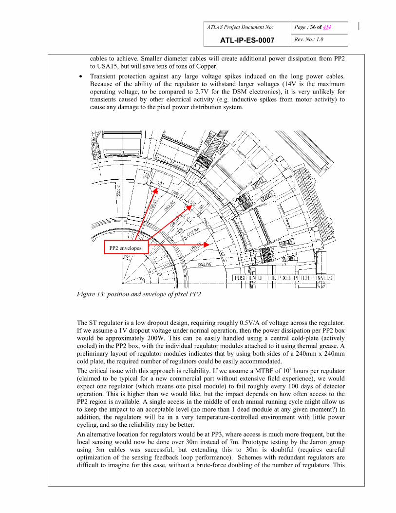
ATLAS Project Document No: Page : 36 of 451
ATL-IP-ES-0007 Rev. No.: 1.0
cables to achieve. Smaller diameter cables will create additional power dissipation from PP2 to USA15, but will save tens of tons of Copper.
• Transient protection against any large voltage spikes induced on the long power cables. Because of the ability of the regulator to withstand larger voltages (14V is the maximum operating voltage, to be compared to 2.7V for the DSM electronics), it is very unlikely for transients caused by other electrical activity (e.g. inductive spikes from motor activity) to cause any damage to the pixel power distribution system.
Figure 13: position and envelope of pixel PP2
The ST regulator is a low dropout design, requiring roughly 0.5V/A of voltage across the regulator. If we assume a 1V dropout voltage under normal operation, then the power dissipation per PP2 box would be approximately 200W. This can be easily handled using a central cold-plate (actively cooled) in the PP2 box, with the individual regulator modules attached to it using thermal grease. A preliminary layout of regulator modules indicates that by using both sides of a 240mm x 240mm cold plate, the required number of regulators could be easily accommodated. The critical issue with this approach is reliability. If we assume a MTBF of 107 hours per regulator (claimed to be typical for a new commercial part without extensive field experience), we would expect one regulator (which means one pixel module) to fail roughly every 100 days of detector operation. This is higher than we would like, but the impact depends on how often access to the PP2 region is available. A single access in the middle of each annual running cycle might allow us to keep the impact to an acceptable level (no more than 1 dead module at any given moment?) In addition, the regulators will be in a very temperature-controlled environment with little power cycling, and so the reliability may be better. An alternative location for regulators would be at PP3, where access is much more frequent, but the local sensing would now be done over 30m instead of 7m. Prototype testing by the Jarron group using 3m cables was successful, but extending this to 30m is doubtful (requires careful optimization of the sensing feedback loop performance). Schemes with redundant regulators are difficult to imagine for this case, without a brute-force doubling of the number of regulators. This
PP2 envelopes

ATLAS Project Document No: Page : 37 of 451
ATL-IP-ES-0007 Rev. No.: 1.0
scheme would use the inhibit capabilities of the regulator to select one of two regulators to drive the output at any given time. Depending on the actual regulator failure modes, such a scheme might not dramatically improve the reliability. At this time, our service design has been made compatible with either using or not using regulators at PP2. This is rendered more challenging by the implementation of the remote sensing in the ST regulator. The base current of the large regulating transistor must flow through the remote sensing ground connection. The vendor claims that this current could be as large as 40mA for our range of load currents. This requires a much lower resistance connection for the sense return wires than would normally be used, making this line intermediate between a signal and a power supply line. From the point of view of its patch-panel functions, PP2 is just a transition from type II cable to type III (more conventional) and plus a possible transition of the cooling pipe size. Detector cooling tubes will not go through PP2 boxes but will be connected in the adjacent area.
8.9 From PP2 to PP3 All the services in this area are permanently installed. There are very strong constraints on the service routing in this area. The tightest constraints occur immediately after PP2 where the services have to follow a complex routing path to pass between the LAr electronics boxes at first and then afterwards to pass between the Tile Calorimeter fingers. There is a strong request to reduce the service occupancy in this area. This is why the voltage drop budget for the pixel cables has been increased to 0.5 V to allow small cable sizing. The cables in this area (type III) are unshielded Copper twisted pairs. They are grouped into homogeneous multi-conductor round cables. The outer size of these cables is chosen as a compromise between flexibility (greater for a smaller OD) and occupancy (lower if more conductors are grouped into a larger OD bundle). Type III inlet and outlet tube bundles are very similar to type II ones, apart from different tube sizes (see figure 14 and 15). Figure 14: type III inlet tube bundle
TRACING TUBE: 8 ODINLET TUBES 5 OD:- 3 OFF (B-layer)- 5 OFF (layer 1&2 and disks)
20
ACTIVEHEATING
INSULATION (s=5 mm MIN)
43 (39 for B-layer)

ATLAS Project Document No: Page : 38 of 451
ATL-IP-ES-0007 Rev. No.: 1.0
Figure 15: type III outlet tube bundle
8.10 PP3 These patch panels are located on service platforms just outside ATLAS volume. No other information is available at the moment.
8.11 From PP3 to service cavern
8.12 Inside the service cavern
9 IDENTIFICATION SCHEME
9.1 Introduction The same numbering rules and conventions apply to the pixel items as well as to the bundles of services internal and external and to the patch panel identification. By convention the numeration starts from the second quadrant (looking from C side) at 180 deg in counterclockwise direction (see figure ..) Side C is chosen as it is the direction of Positive Z in the detector coordinate system.
OUTLET TUBES:- 10 OD 3 OFF (B-layer)- 9 OD 5 OFF (layer 1&2 and disks)
19(20 for B-layer)
INSULATION (s=5 mm MIN)
55 (37 for B-layer)

ATLAS Project Document No: Page : 39 of 451
ATL-IP-ES-0007 Rev. No.: 1.0
0
C SIDE VIEWQUADRANT NO. 1
9.2 Barrel services The numeration scheme adopted for the barrel components is coherent with the different assembly levels, with bottom-up approach: • Layer • Bi-stave • Stave • Module • Type n cable bundles • Type n cables • Inlet tubes, outlet tubes The three barrel layers are identified with the following code:
Ll Where l is the layer number: • B-layer = 0 • Layer 1 = 1 • Layer 2 = 2 Each bi-stave assembly is identified with the following code: Ll bb Where: bb is the bi-stave number of the given layer. Bi-stave no. is sequential clockwise, bi-stave no. 1 is the first bi-stave with the exhaust tube in quadrant 1. bb ranges: • B-layer: 1 – 11 • Layer 1: 1 – 19 • Layer 2: 1 – 26

ATLAS Project Document No: Page : 40 of 451
ATL-IP-ES-0007 Rev. No.: 1.0
The stave is identified with the following code: Ll bb p Where p is the position on the bi-stave (1 or 2, clockwise looking from C side). Coherently with the stave naming convention, the inlet and outlet tubes are identified as follows: Ll bb p s t Where: t = tube type: t = I for capillary t = O for exhaust s = side direction: A or C In the same way the cable bundles are identified as follows: Ll bb p s nn Where nn is bundle type: nn = 06 for six module cable bundle (layer 1&2)
nn = 07 for seven module cable bundle (layer 1&2) nn = 13 for thirteen module cable bundle (B-layer)
By convention the first stave of each bi-stave will have the 7 module bundle of cables going out always from side C. The orientation of the module on the stave and the position of the pigtail connection relative to the detector z axis is shown in figure…. Figure .. shows also the adopted criteria for the identification of the module position along the stave.
Z
A SIDE C SIDE
7 MODULE BUNDLE
7 MODULE BUNDLE 6 MODULE BUNDLE
6 MODULE BUNDLE
2C1C01A6A
ORIENTATION OF TYPE 0 CABLE BUNDLE FOR FIRST STAVE OF EACH BI-STAVE (LAYER 1&2)
ORIENTATION OF TYPE 0 CABLE BUNDLE FOR SECOND STAVE OF EACH BI-STAVE (LAYER 1&2)
ORIENTATION OF 13 TYPE 0 CABLE BUNDLE FOR THE B-LAYER
Finally each single cable is identified by the following code: Ll bb p s nn mm

ATLAS Project Document No: Page : 41 of 451
ATL-IP-ES-0007 Rev. No.: 1.0
Where mm is the module position along the stave: mm = 6A, 5A, 4A, 3A, 2A, 1A, 0, 1C, 2C, 3C, 4C, 5C, 6C For example the code L1 02 1 C 06 2C indicates a cable: - belonging to a 6 module bundle - going along C side - connected to 2C module - of 1st stave - on second bi-stave - of layer 1
9.3 Disk services . A similar system is presented for sector identification. Unlike the staves, where a Bi-Stave assembly is a fundamental unit of the Local supports, in the forward regions, sectors are the fundamental assembly units and are interchangeable. This causes some logical inconsistencies for the cooling circuits, and with module enumeration. These differences are documented here. Each Disk is identified by number and side, with Disk 1 of each side being closest to the IP. Disk enumerations are preceded with the letter “D.” Disk enumeration follows the form Dd s Where d is the position number and s is the side (A or C). The first disk on side C located at Z= +495mm, is called D1C.
• D1C Z= +495mm D1A Z= -495mm • D2C Z= +570mm(chk)D2A Z= -570mm • D3C Z= 650mm D3A Z= -650mm
Each sector can be uniquely identified with a number of the form: Dd s-Sn Disk-Sector Where n is a number (1-8). As per the convention, sector number 1 is numbered clockwise from ATLAS minus X axis. “D1C-S1” is a sector on the first disk, on the negative X side, closest to the X axis, in the positive Y half plane. The sector number is also useful alone, and should be preceded by an S, for identification of sector position on any disk. All disks are identical and interchangeable until services are attached to them. On a given sector, each module can be identified with a number 1-6. With Sector Datum –A- (mount-side) facing away, the modules will be numbered 1-6, left to right. This puts modules [1,3,5] on the non-mount-side facing, and modules [2,4,6] on the mount-side facing. For consistency with interchangability, this numbering is relative to the sector, not the ATLAS coordinate system. Relative to ATLAS, this means that the modules are always numbered clockwise if looking at them from the IP. What this means is that on side C each sector’s modules will be numbered 1-6 counter-clockwise, and clockwise on side A (see fig****). Dd s-Sn-Mm DiskSectorModule With the above scheme, each module in the forward detectors can be identified, and it’s position ascertained. This enumeration will extend to the cables which service each module. Where a given

ATLAS Project Document No: Page : 42 of 451
ATL-IP-ES-0007 Rev. No.: 1.0
cable services several modules, a dash can be introduced to indicate which range of modules are serviced e.g. Cable-Name-D3C-S7-M1-6 might be appropriate for the type 1 flex part of PP0. Notice that M1-6 is all of the modules on a given sector, meaning that it could be dropped, unless we keep module range as part of the cable name descriptor. Sector cooling is also done in pairs, because of sector interchangability, it is inconvenient to specify an inlet and an outlet on a sector, as it may be reversed in another pair. To uniquely identify a sector cooling circuit, it is necessary to specify both the disk, and the sector pair involved. Dd s-Sn-n’ DiskSector inlet-Sector Outlet Where “n” and “n(prime)” are sector numbers, quoted in the order of inlet and outlet. To identify each tube uniquely, it is necessary to append an I or an O as with the stave numbering system. Dd s-Sn-n’/t Therefore, D1C-S8-1/O is the exhaust tube attached to sector 1. The position of the U-tube is between S1 and S8 on disk D1C. D1C-S8-1/I is the inlet attached to sector 8 of the same circuit. D3A-S4-M3 resolves to: The last (clockwise looking away from IP module) on the IP-side of the sector. On the 4th sector on the third disk of the A side of the detector. With this information it is also possible to guess the physical location to a few cubic cm. This module is at Z= - 650, X= +175, Y= +20. D2C-S5-4 is a cooling circuit on the second disk of side C straddling the +X axis. (U-tube is located on the +X axis. D1A-S5-4/I is the inlet to the cooling circuit of the first disk on the opposite side which enters sector S5.
10 OVERALL SERVICE INVENTORY (GROUPING AND OCCUPANCY) According to the identification and grouping criteria previously established, the first important step is to map modules/stave(sector) serviced to octant position of relevant cables and pipes. This mapping propagates throughout the entire system. There is a non-uniform distribution of services in different octants/quadrants (B-layer) due to phi asymmetries of services in barrel and disk areas. The final distribution of services in different octants/quadrants is not yet settled however the best and worst cases are known. Provisions will be made in order to have the best octant/quadrant (lowest occupancy) passing through the worst gaps (smallest cross section area) in between LAr electronics boxes. The following table features the number of pipes and 6/7 module cable bundles for the best and worst octant/quadrant.
OCTANT-
QUADRANTTYPE
No. of cooling pipes No. of 7 module bundles No. of 6 module bundle

ATLAS Project Document No: Page : 43 of 451
ATL-IP-ES-0007 Rev. No.: 1.0
Barrel Disk Barrel barrel disk
Best 2 1 5 5 3 La
yer
1&2
and
disk
s
Worst 3 2 6 6 3
Best 2 5 5 B
-laye
r
Worst 3 6 6
The occupancy for type II and III services of the worst outer layer octant and B-layer quadrant has been estimated. The service breakdown for the worst octant and quadrant includes all relevant local services. The global services (gas purging lines, environmental temperature monitors and thermal barrier power supplies/temperature sensors) are assumed to be routed through the gaps with more space available and lower occupancy. The following tables give the calculated occupancy for the worst octant of outer layers&disks and for worst quadrant of B-layer and for type II and III services.
Layer 1&2 + disks WORST OCTANT OCCUPANCY
TYPE II
service cable type composition OD number spares PF area tot (cm2) VDD h 7x2 11 15 9x2 1.78 25.4VDDA k 7x2 12 15 9x2 1.78 30.2NTC-MOD c 7x2 5 15 9x2 1.78 5.2HV d 7x1 4.5 15 9x1 1.78 4.2SENSE-MOD g 7x1 3.5 30 18x1 1.78 5.1SENSE-MOD-RET m 7x1 6 30 18x1 1.78 15.1VVDC j 2x2 5.5 15 1.78 6.3SENSE-OPTO g 7x1 3.5 5 5x1 1.78 0.9SENSE-OPTO-RET m 7x1 6 5 5x1 1.78 2.5OPTO c 7x2 5 15 45x2 1.78 5.2subtotal cables 100.2INLET COOLING 5+2 8.0OUTLET COOLING 5 14.5Subtotal tubes 22.5OPTICAL FIBERS 8-way ribbon 8x1 2x15 2.0Gran total 124.7
Layer 1&2 + disks WORST OCTANT OCCUPANCY
TYPE III
service cable type composition OD number spares PF area tot (cm2) VDD a 7x2 14 15 9x2 1.78 41.1VDDA b 7x2 15 15 9x2 1.78 47.2NTC-MOD c 7x2 5 15 9x2 1.78 5.2HV d 7x1 4.5 15 9x1 1.78 4.2SENSE-MOD g 7x1 3.5 30 18x1 1.78 5.1

ATLAS Project Document No: Page : 44 of 451
ATL-IP-ES-0007 Rev. No.: 1.0
SENSE-MOD-RET f 7x1 7 30 18x1 1.78 20.5VVDC e 2x2 6 15 1.78 7.5SENSE-OPTO g 7x1 3.5 5 5x1 1.78 0.9SENSE-OPTO-RET f 7x1 7 5 5x1 1.78 3.4OPTO c 7x2 5 15 45x2 1.78 5.2NTC-ACT-HEAT c 7x2 5 1 3x2 1.78 0.3ACT-HEAT e 2x2 6 1 1.78 0.5NTC-RET-TUBE c 7x2 5 2 4x2 1.78 0.7subtotal cables 142.0INLET COOLING 5+2 8.0OUTLET COOLING 5 15.5Subtotal tubes 23.5OPTICAL FIBERS 16x12-way
ribbon trunking
16x12 10 2 2x12 1.78 2.8
Gran total 168.3
B-Layer WORST QUADRANT OCCUPANCY
TYPE II
service cable type composition OD number spares PF area tot (cm2) VDD k 7x2 12 12 6x2 1.78 24.1VDDA a 7x2 14 12 6x2 1.78 32.9NTC-MOD c 7x2 5 12 6x2 1.78 4.2HV d 7x1 4.5 12 6x1 1.78 3.4SENSE-MOD g 7x1 3.5 24 12x1 1.78 4.1SENSE-MOD-RET m 7x1 6 24 12x1 1.78 12.1VVDC p 7x2 8 12 1.78 10.7OPTO c 7x2 5 12 36x2 1.78 4.2subtotal cables 95.7INLET COOLING 5+2 6.4OUTLET COOLING 5 10.0Subtotal tubes 16.4OPTICAL FIBERS 8-way ribbon 8x1 2x18 2.3Gran total 114.4
B-Layer WORST QUADRANT OCCUPANCY
TYPE III
service cable type composition OD number spares PF area tot (cm2) VDD b 7x2 15 12 6x2 1.78 37.7VDDA n 5x2 15 18 6x2 1.78 56.6NTC-MOD c 7x2 5 12 9x2 1.78 4.2HV d 7x1 4.5 12 9x1 1.78 3.4SENSE-MOD g 7x1 3.5 24 18x1 1.78 4.1SENSE-MOD-RET f 7x1 7 24 18x1 1.78 16.4VVDC p 7x2 8 12 1.78 10.7SENSE-OPTO g 7x1 3.5 12 6x1 1.78 2.1

ATLAS Project Document No: Page : 45 of 451
ATL-IP-ES-0007 Rev. No.: 1.0
SENSE-OPTO-RET f 7x1 7 12 6x1 1.78 8.2OPTO c 7x2 5 12 36x2 1.78 4.2NTC-ACT-HEAT c 7x2 5 1 3x2 1.78 0.3ACT-HEAT e 2x2 6 1 1.78 0.5NTC-RET-TUBE c 7x2 5 1 1x2 1.78 0.3subtotal cables 148.8INLET COOLING 5+2 7.6OUTLET COOLING 5 12.4Subtotal tubes 20.0OPTICAL FIBERS 16x12-way
ribbon trunking
16x12 10 3 4x12 1.78 4.2
Gran total 173.0
Two alternative options to the current baseline (voltage regulator at PP3 and no transition in size for type III cables) have been considered in order to evaluate possible ways of reducing the occupancy in the critical gap in between LAr electronics boxes at the lower radius location. This is the actual bottleneck immediately affecting the gap size along the cryostat side. The first option would consist of type III cables split in two parts with different sizes: • First part (type 0.a cables) with same (small) size as type II cables • Second part (type 3.b cables) with bigger cables sized to keep the overall voltage drop across
type III cable within the specifications The transition between type 3.a and type 3.b would be permanent and located immediately after the bend at the exit of Tile fingers. This option would allow to pass through the critical area with smaller cable size and hence to reduce the occupancy. The second option consists of the first option, but with voltage limiters in PP2. The second option allows for a further reduction of the occupancy in the critical gap because the sense wires are no longer going out of PP2, but of course it implies a much more aggressive design. The following table summarises the gap occupancy of type II and type III cables for worst octant/quadrant comparing the baseline with the two alternative options.
TYPE III OCCUPANCY (cm2) TYPE II
baseline Option A Option B Barrel & disk worst octant 125 168 136 105
B-layer worst quadrant 115 173 136 105
The full service inventory with the detailed list of services for each octant will be prepared later on as soon as the design and technological choices in PP2 area will be more settled.