Embed Size (px)
Citation preview

Research ArticleSuppression of Specular Reflections by Metasurface withEngineered Nonuniform Distribution of Reflection Phase
Xin Mi Yang12 Ge Lan Jiang1 Xue Guan Liu1 and Cheng Xiang Weng3
1School of Electronics and Information Engineering Soochow University Suzhou 215006 China2State Key Laboratory of Millimeter Waves Southeast University Nanjing 210096 China3Electronic Countermeasure Laboratory Air Force Early Warning Academy Wuhan 430019 China
Correspondence should be addressed to Xin Mi Yang yangxinmisudaeducn
Received 9 November 2014 Accepted 8 January 2015
Academic Editor Sanming Hu
Copyright copy 2015 Xin Mi Yang et al This is an open access article distributed under the Creative Commons Attribution Licensewhich permits unrestricted use distribution and reproduction in any medium provided the original work is properly cited
Wemake preliminary investigations on a new approach to reducing radar cross section (RCS) of conducting objectsThis approachemploys novel planar metasurfaces characterizing nonuniform distribution of reflection phase The operation principle of thisapproach and the design rule of the associated metasurfaces are explained using a simplified theoretical model We then present adesign example of such metasurfaces in which three-layer stacked square patches with variable sizes are utilized as the reflectingelements The proposed RCS-reduction approach is verified by both numerical simulations and measurements on the exampleunder the assumption of normal plane wave incidence It is observed that in a fairly wide frequency band (from 36 to 55 GHz)the presented example is capable of suppressing the specular reflections of conducting plates significantly (by more than 7 dB) fortwo orthogonal incident polarizations
1 Introduction
Reduction of target radar cross section (RCS) for military orcivilian applications has been a subject of extensive studiesin both scientific and engineering communities for decadesThe existing RCS-reduction strategies can be classified intotwo categories One is decreasing or even canceling thescattered energy and the other is reshaping the scatteringpattern Traditionally the radar absorbing material (RAM)is adopted for the first category while the second categoryis usually achieved through shaping of target [1ndash4] Recentlygreat efforts have been made for the sake of improving thetraditional RAM technology For instance reduced RAMthickness has been achieved by employing artificial magneticconductor (AMC) or reactive impedance ground as thebacking panel of RAM [5ndash7] It is worth mentioning thatthe rapidly growing research field of metamaterials hascontributed a completely new strategy called invisibility cloak[8 9] which can be grouped into the first category Theinvisibility cloak is a kind of inhomogeneous wrappage thatcould steer the incoming electromagnetic waves smoothly
around the hidden object and return them to their originaltrajectory making the object almost invisible (ie have noscattered field) New ideas have emerged regarding the sec-ond category of RCS-reduction techniques these years as well[10ndash14] For example it was proposed by Paquay et al thatby combining AMC and perfect electrical conductor (PEC)cells in a chessboard-like configuration the cancelation ofreflections from these two kinds of cells would effectivelyreduce the specular reflections and hence the RCS of planarconducting plate [10] In addition some researchers have paidattention tometamaterial coatings with randomly distributedrefractive indices or gradients of refractive index [11ndash13]Such coatings are capable of suppressing remarkable lobesof conducting plates by creating diffuse reflections in frontof these plates In 2014 Wang et al proposed a designof broadband and broad-angle low-scattering metasurfacebased on a hybrid optimization algorithm [14]
In this paper we make further investigations on RCS-reduction schemes characterizing redistribution of scat-tered energy by making use of novel metasurfaces withnonuniformly distributed reflection phase The rest of
Hindawi Publishing CorporationInternational Journal of Antennas and PropagationVolume 2015 Article ID 560403 8 pageshttpdxdoiorg1011552015560403
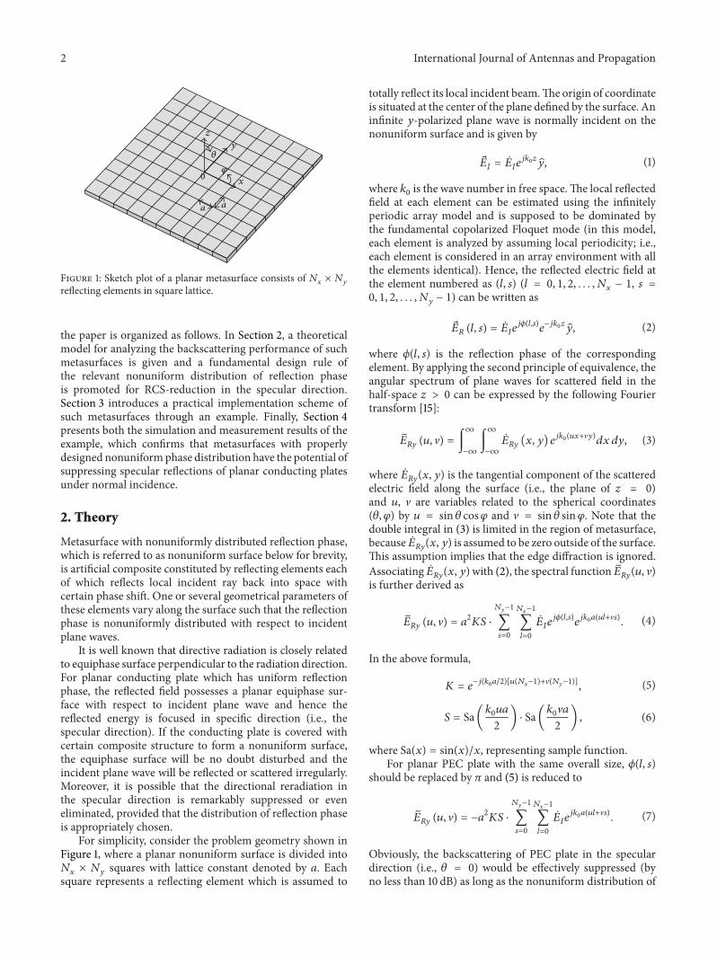
2 International Journal of Antennas and Propagation
120579
a a
x
z
120593
y
0
Figure 1 Sketch plot of a planar metasurface consists of 119873119909times 119873119910
reflecting elements in square lattice
the paper is organized as follows In Section 2 a theoreticalmodel for analyzing the backscattering performance of suchmetasurfaces is given and a fundamental design rule ofthe relevant nonuniform distribution of reflection phaseis promoted for RCS-reduction in the specular directionSection 3 introduces a practical implementation scheme ofsuch metasurfaces through an example Finally Section 4presents both the simulation and measurement results of theexample which confirms that metasurfaces with properlydesigned nonuniformphase distribution have the potential ofsuppressing specular reflections of planar conducting platesunder normal incidence
2 Theory
Metasurface with nonuniformly distributed reflection phasewhich is referred to as nonuniform surface below for brevityis artificial composite constituted by reflecting elements eachof which reflects local incident ray back into space withcertain phase shift One or several geometrical parameters ofthese elements vary along the surface such that the reflectionphase is nonuniformly distributed with respect to incidentplane waves
It is well known that directive radiation is closely relatedto equiphase surface perpendicular to the radiation directionFor planar conducting plate which has uniform reflectionphase the reflected field possesses a planar equiphase sur-face with respect to incident plane wave and hence thereflected energy is focused in specific direction (ie thespecular direction) If the conducting plate is covered withcertain composite structure to form a nonuniform surfacethe equiphase surface will be no doubt disturbed and theincident plane wave will be reflected or scattered irregularlyMoreover it is possible that the directional reradiation inthe specular direction is remarkably suppressed or eveneliminated provided that the distribution of reflection phaseis appropriately chosen
For simplicity consider the problem geometry shown inFigure 1 where a planar nonuniform surface is divided into119873119909times 119873119910squares with lattice constant denoted by 119886 Each
square represents a reflecting element which is assumed to
totally reflect its local incident beamThe origin of coordinateis situated at the center of the plane defined by the surface Aninfinite 119910-polarized plane wave is normally incident on thenonuniform surface and is given by
119868= 1198681198901198951198960119911119910 (1)
where 1198960is the wave number in free spaceThe local reflected
field at each element can be estimated using the infinitelyperiodic array model and is supposed to be dominated bythe fundamental copolarized Floquet mode (in this modeleach element is analyzed by assuming local periodicity ieeach element is considered in an array environment with allthe elements identical) Hence the reflected electric field atthe element numbered as (119897 119904) (119897 = 0 1 2 119873
119909minus 1 119904 =
0 1 2 119873119910minus 1) can be written as
119877(119897 119904) =
119868119890119895120601(119897119904)
119890minus1198951198960119911119910 (2)
where 120601(119897 119904) is the reflection phase of the correspondingelement By applying the second principle of equivalence theangular spectrum of plane waves for scattered field in thehalf-space 119911 gt 0 can be expressed by the following Fouriertransform [15]
119864119877119910(119906 V) = int
infin
minusinfin
int
infin
minusinfin
119877119910(119909 119910) 119890
1198951198960(119906119909+V119910)119889119909 119889119910 (3)
where 119877119910(119909 119910) is the tangential component of the scattered
electric field along the surface (ie the plane of 119911 = 0)and 119906 V are variables related to the spherical coordinates(120579 120593) by 119906 = sin 120579 cos120593 and V = sin 120579 sin120593 Note that thedouble integral in (3) is limited in the region of metasurfacebecause
119877119910(119909 119910) is assumed to be zero outside of the surface
This assumption implies that the edge diffraction is ignoredAssociating
119877119910(119909 119910)with (2) the spectral function119864
119877119910(119906 V)
is further derived as
119864119877119910(119906 V) = 1198862119870119878 sdot
119873119910minus1
sum
119904=0
119873119909minus1
sum
119897=0
119868119890119895120601(119897119904)
1198901198951198960119886(119906119897+V119904) (4)
In the above formula
119870 = 119890minus119895(11989601198862)[119906(119873119909minus1)+V(119873119910minus1)] (5)
119878 = Sa(1198960119906119886
2) sdot Sa(
1198960V1198862
) (6)
where Sa(119909) = sin(119909)119909 representing sample functionFor planar PEC plate with the same overall size 120601(119897 119904)
should be replaced by 120587 and (5) is reduced to
119864119877119910(119906 V) = minus1198862119870119878 sdot
119873119910minus1
sum
119904=0
119873119909minus1
sum
119897=0
1198681198901198951198960119886(119906119897+V119904) (7)
Obviously the backscattering of PEC plate in the speculardirection (ie 120579 = 0) would be effectively suppressed (byno less than 10 dB) as long as the nonuniform distribution of
International Journal of Antennas and Propagation 3
400
400
300
300
200
200
100
10000
0
minus100
minus200
minus300
minus400
minus500
y-a
xis (
mm
)
x-axis (mm)
(deg
)Figure 2 An instance of two-dimensional nonuniform distributionof reflection phase in degree which is expected to significantlyreduce the specular reflection of planar conducting plates
reflection phase 120601(119897 119904) satisfies the relation expressed by thefollowing inequation
10038161003816100381610038161003816100381610038161003816100381610038161003816
119873119910minus1
sum
119904=0
119873119909minus1
sum
119897=0
119890119895120601(119897119904)
10038161003816100381610038161003816100381610038161003816100381610038161003816
le radic01 sdot 119873119909119873119910 (8)
Such a conclusion is in accordance with the antenna arraytheory and similar conclusions could be drawn for the casesof off-normal incidence
As an example consider a planar nonuniform surfacecontaining 10 times 10 reflecting elements It has the two-dimensional phase distribution as shown in Figure 2 Thisdistribution is generated by randomly selecting phases inthe range [minus504 deg 40 deg] With such a distribution theamplitude of the double summation in (8) is calculated to be2315 which is much smaller than 119873
119909119873119910= 100 According
to the theoretical model presented above the intensity ofspecular far-field scattering of the designed metasurface is1277 dB lower than that of naked conducting surface with thesame overall size when both surfaces are illuminated by 119909- or119910-polarized normally incident plane waves We remark thatthe choice of the distribution in Figure 2 is rather arbitraryIn fact the condition indicated by (8) is very weak and thereare numerous possibilities for reflection-phase distributionswhichmeet this conditionTherefore wideband performanceis in prospect even though the phase distribution variesviolently in band This is beneficial when broadband RCS-reduction behavior is required since the phase distribution ofrealistic nonuniform surface is usually frequency-dependentas will be shown in the next section
3 Implementation of Nonuniform Surface
Various radiators can be used as the reflecting elementsof nonuniform surfaces In particular microstrip radiatorssuch as metallic patches dipoles and loops are suitablefor circumstances where conformality and compactness are
required [16ndash19] Figure 3 demonstrates a typical reflectingelement in microstrip form which characterizes three-layerstacked square patches of variable size The stacked-patchelement occupies an 119886 times 119886 square area in the 119909-119910 plane and isbacked with a conducting groundThe side lengths of patcheson the bottom middle and top layers are denoted by 119889 119903
1119889
and 1199032119889 respectively where 119903
1and 1199032are proportional factors
with 1199032lt 1199031lt 1 Each of the three patches is supported by
a piece of thin dielectric substrate which is also 119886 times 119886 in sizeThe patch thickness and substrate thickness for each layer arerepresented by 119905
119898and 119905119904 respectively Moreover Figure 3(b)
indicates that every two neighboring layers (including theground layer and the three patch layers) are separated by airwith the separation distances denoted by ℎ
119894(119894 = 1 2 3)
As is well known the microstrip patch over a groundplane response resonantly to incident plane waves leading tosensitive reflection phase with respect to frequency variationsnear resonance The resonant frequency mainly depends onthe side length of patch and the reflection phase withincertain frequency band can be effectively tuned by varyingthe side length By stacking multiple patches a multiresonantbehavior is obtained and the tuning range of reflectionphase can be expanded greatly [20 21] Moreover stackingmultiple patches is also helpful in enlarging the frequencybandwith linear response of reflection phase which is criticalin increasing the operational bandwidth of the nonuniformsurface The air separation employed under each patch layerfurther broadens the frequency band with sufficiently largetuning range of phase and results in a smoother and morelinear phase variation versus side length 119889
As an example a parametric study has been made on thethree-layer stacked-patch element with certain specificationsEach patch layer of the element under study is fabricatedfrom F4B copper-clad laminate with copper thickness of 119905
119898=
0035mm substrate thickness of 119905119904= 043mm and dielectric
constant of 265 minus 11989500053 The element size the relative sizesof the stacked patches and the air separations are consideredfixed (119886 = 45mm 119903
1= 068 119903
2= 05 and ℎ
1= ℎ2=
ℎ3= 4mm) and only the side length of bottom patch 119889
is the independently tunable variable The parametric studyis performed via numerical simulations using the commer-cial electromagnetic solver CST Microwave Studio (MWS)Figure 3(c) shows the relation curve of simulated reflectionphase at 4GHz against the dimension 119889 for the relevantstacked-patch elements The reflection phase is associatedwith the fundamental copolarized Floquet mode with respectto normally incident plane waves polarized along the 119909-(or 119910-) axis when periodic boundary conditions (PBCs) areassumed around the element in both the 119909 and 119910 directionsThe reference plane just overlaps with the plane of top patchIt is seen from Figure 3(c) that the tuning range of reflectionphase at 4GHz is greater than 500∘
Figure 4 illustrates a realistic nonuniform surface formedby arranging the three-layer stacked-patch elements in 119886 times
119886 square lattice It is consistent with the model shown inFigure 1 The nonuniform distribution of reflection phase isachieved by varying the dimension119889 and keeping all the otherparameters (ie 119905
119904 119905119898 1199031 1199032 and ℎ
119894) constant in the surface
We remark that the structure in Figure 4 is quite similar to
4 International Journal of Antennas and Propagation
y
xz
Ey
Plane wave
Conducting plate
(a)
d
r1d
r2d
a
a
y
x
x
z
ts tm
h3h2
h1
(b)
d
a
a
y
x
r1d
r2d
100
0
minus100
minus200
minus300
minus400
minus500
minus60010 20 30 40
d (mm)
Refle
ctio
n ph
ase (
deg)
(c)
Figure 3 Reflecting element characterizing three-layer stacked square patches of variable size (a) Oblique view (b) Elevation view and sideview In the elevation view the second and third substrate layers are omitted to show all the three patch layers clearly (c) Typical design curverelating reflection phase at 4GHz with the dimension 119889 for the stacked-patch elements with certain specifications
that of microstrip reflectarray [19] However the traditionalreflectarray should be excited by certain feed antenna andis designed to produce directional reradiation while thenonuniform surface proposed here has no feed antenna andis designed to destroy the directional reflection with respectto incoming plane waves
An instance of nonuniform surface based on the stacked-patch elements has been designed and the correspondingfabricated sample is shown in Figure 5(a) This instancecomprises 10 times 10 elements which are characterized by thespecifications mentioned above Hence the total thickness
(from the top patch to the ground plane) of the instanceis about 133mm The instance was designed to possess thetwo-dimensional phase distribution shown in Figure 2 at4GHz Given this phase distribution the dimension 119889 ofall the constituent elements for the nonuniform surface wasdetermined using the design curve shown in Figure 3(c)Thefinal distribution of dimension 119889 is shown in Figure 5(b) Itshould be remarked that the phase distribution here avoidsdrastic change of patch size between neighboring elementsso that the periodic array model for element evaluationmentioned above maintains enough accuracy
International Journal of Antennas and Propagation 5
z
y
x
120579
120593
Conductingplate
Figure 4 Nonuniform surface consisting of three layers of squarepatches with variable size above a conducting ground All thesubstrate layers are set transparent so that the ground layer and thebottom and middle patch layers could be shown
Due to the frequency-dependent phase response of thestacked-patch element the phase distribution of the nonuni-form surface changes with frequency However for ourpresented instance the nonuniform feature of the phase dis-tributionwithin a sufficiently large range remains over a fairlywide frequency band that is from about 3GHz to 6GHzFigure 6 demonstrates the specular far-field reflectance forthe instance in this band (circle) This reflectance curvewhich assumes normal incidence and 119909- or 119910-polarizationis normalized to that of naked conducting surface and iscalculated from the frequency-dependent phase distributionusing the aforementioned theoretical model Remarkablesuppression of specular reflection throughout the band isobserved from Figure 6
4 Simulation and Measurement Results
In order to verify the nondirectional reflection property of thenonuniform surface full-wave simulations are conducted forthe instance presented above with the aid of CSTMWS Boththe 119909- and 119910-polarized plane waves with normal incidenceare considered in the simulations For both polarizations thesimulated specular far-field reflectance curves normalized tothat of naked conducting surface are also shown in Figure 6(solid and dashed lines) As is expected these two curvesare in good consistency with the theoretical curve (circle)Figure 6 also indicates that the two simulated curves areslightly different from each otherThis is because the nonuni-form surface as instance has no rotational symmetry withrespect to its central normal Our theoretical model ignoresthis asymmetry and offers the same calculated reflectanceresults for both polarizations However such an ignorance orapproximation does not prevent themodel from providing uswith acceptable predictions of backscattering performance ofnonuniform surfaces A further inspection on the simulatedbackscattering patterns of both the nonuniform surface andthe naked conducting surface reveals that the suppressionof specular reflections is achieved through unequally reallo-cating most of the scattered energy to various off-specular
x
y z
(a)
45
40
35
30
25
20
(mm
)
400
400
300
300
200
200
100
10000
y-a
xis (
mm
)
x-axis (mm)
(b)
Figure 5 (a) Photograph of a nonuniform surface sample composedof three-layer stacked-patch elements Note that the bottom rowof elements is buried in foams and can not be seen (b) Two-dimensional distribution of dimension 119889 for patches on the bottomlayer (unit millimeters)
directions in the 119911 gt 0 half-space (ie 0 le 120579 lt 90) Asan example Figure 7 compares the simulated backscatteringpatterns between the nonuniform surface and the nakedconducting surface at 4GHz for the 119910-polarized normalincidence
Backscattering measurements have also been conductedconcerning the nonuniform surface sample shown inFigure 5 The measurements consist of two stages whichemploy almost the same experimental setup Figure 8 showsthe experimental setup for the first stage where a linearlypolarized high-gain horn antenna is placed right in front ofthe nonuniform surface sample with a distance of 3 metersand the central normal of the sample surface is aligned withthe symmetry axis of the horn aperture The horn antenna isalso connected to a single port of an Agilent N5230C vectornetwork analyzer (VNA) through a flexible coaxial cableThewhole setup is situated in an anechoic chamber to minimizeenvironmental interferences During measurement theVNA provides source microwave signals for the antenna andthe main beam emitted from the horn antenna impinges on
6 International Journal of Antennas and Propagation
0
minus5
minus10
minus15
minus20
minus25
minus303 4 5 6
(dB)
f (GHz)
Simulation y-polarizedSimulation x-polarizedTheoretical calculation
Figure 6 Theoretical and simulated results of the normalizedspecular far-field reflectance of the nonuniform surface as instanceunder normal incidence
the sample surface The back-scattered or reflected powerfrom the sample is received by the same horn and thendetected by the VNA Note that the power reflected by thehorn itself also enters the VNA in the meantime By applyingthe gated-reflect-line (GRL) calibration technique providedby the time-domain analysis kit installed in the VNA theinfluence of the power reflected by the horn is removedand the resultant reflection coefficient data read from theVNA is only related to the reflection from the sample Twocases of incident beams are considered in the first stage Forthe first case the horn is arranged to allow a 119910-polarizedincident beam with respect to the sample shown in Figure 5By simply rotating the sample 90∘ around its central normalthe other case of incident beam with 119909-polarization canbe achieved afterwards The reflection coefficient data indecibels read from the VNA are recorded for both cases Asto the second stage of measurement the nonuniform surfacesample is replaced by an ordinary square metallic platewhich possesses the same size as the sample The reflectioncoefficient data in decibels given by the VNA at this stage isalso recorded The specular reflectance of the nonuniformsurface sample normalized to that of the square metallicsurface for both incident polarizations can then be obtainedby subtracting the newly recorded data from those two setsof data measured at the first stage respectively
Figure 9 shows the experimental normalized specularreflectance of the nonuniform surface sample for both inci-dent polarizations It is observed that in the presence ofthe sample the directional specular reflection of the metallic
1
08
06
04
02
0
minus02
minus04
minus06
minus08
minus1minus1 minus05 0 05 1
0
minus5
minus10
minus15
minus20
minus25
minus30
minus35
minus40
minus45
minus50
(dB)
u = sin(120579) cos(120593)
=sin(120579)sin(120593)
(a)
1
08
06
04
02
0
minus02
minus04
minus06
minus08
minus1minus1 minus05 0 05 1
0
minus5
minus10
minus15
minus20
minus25
minus30
minus35
minus40
minus45
minus50
(dB)
u = sin(120579) cos(120593)
=sin(120579)sin(120593)
(b)
Figure 7 Simulated backscattering patterns under 119910-polarizednormal incidence at 4GHz for (a) the nonuniform surface asinstance and (b) the naked conducting surfaceThe far-field intensityinvolved in this figure is the synthesized quantity radic|119864
120579|2 + |119864
120593|2
Both patterns are normalized to the specular far-filed intensity ofthe conducting surface and the values below minus50 dB have all beentruncated
surface in the band from 36 to 55 GHz is suppressed bymore than 10 dB and 7 dB for the 119910- and 119909-polarized incidentbeams respectively Hence the potential of the nonuniformsurface to reduce RCS of conducting objects over a fairlywide frequency band is well demonstrated The simulatedreflectance is also shown in Figure 9 for comparison Wenote that the measured reflectance minima appear at higherfrequencies compared with their simulated counterpartsHowever the measured and simulated reflectance curves arein qualitative agreement if we uniformly shift the measuredcurves towards lower frequency The discrepancy between
International Journal of Antennas and Propagation 7
Sample
HornTo VNA
Figure 8 Experimental setup formeasuring the specular reflectanceof the nonuniform surface sample under normal incidence
0
minus5
minus10
minus15
minus20
minus25
minus30
minus35
minus40
minus453 4 5 6
(dB)
f (GHz)
Simulation y-polarizedSimulation x-polarized
Measurement y-polarizedMeasurement x-polarized
Figure 9 Experimental results of the normalized specularreflectance of the nonuniform surface sample with respect to both119909- and 119910-polarized normally incident wavesThe 119909 and 119910 directionsare indicated by Figure 5(a)
the simulated andmeasured results ismainly attributed to theinaccuracy of the substrate permittivity the fabrication andassembly error of the sample and the differences between theexperimental setup and the simulation configuration In ourexperimental setup the sample is in the radiating near-field(Fresnel) region of the horn antenna and the local incidentrays for most of the reflecting elements are just roughlyperpendicular to the element surface In otherwords the finalexperimental reflectance is not in a strict far-field sense andmost of the reflecting elements underwent oblique incidencein the experiment Because the first-order resonant frequencyof metallic patch increases as the incidence angle grows theeffective operating band of the metasurface moved to higherfrequency region in the experiment
5 Conclusions
We have demonstrated that planar metasurface with nonuni-formly distributed reflection phase referred to as nonuni-form surface is capable of suppressing the specular reflec-tions of conducting plates by scattering most incident energyin off-specular directions A general condition under whichthe nonuniform surface could operate effectively has beenderived using a simplified theoretical model Based on thiscondition an instance of nonuniform surface composedof three-layer stacked-patch elements has been designedBoth simulation and measurement results for the designexample confirm that the nonuniform surface is an effectiveapproach of RCS-reduction for conducting objects and hasthe potential of providing broadband performance
Conflict of Interests
The authors declare that there is no conflict of interestsregarding the publication of this paper
Acknowledgments
This work was supported in part by the Natural ScienceFoundation of Jiangsu Province under Grant BK20130326 inpart by the National Natural Science Foundation of Chinaunder Grant 61301076 in part by theOpen Research Programof State Key Laboratory of Millimeter Waves in China underGrant K201417 and in part by theNatural Science Foundationof the Higher Education Institutions of Jiangsu Provinceunder Grant 12KJB510030
References
[1] W W Salisbury ldquoAbs orbent body for electromagnetic wavesrdquoU S Patent 2 599 944 June 1952
[2] E F Knott J F Shaeffer and M T Tuley Radar Cross SectionArtech House London UK 1993
[3] Y Z RuanRadar Cross Section and Stealth Technology NationalDefence Industry Press Beijing China 1998
[4] J AAdam ldquoHow to design an invisible aircraftrdquo IEEE Spectrumvol 25 no 4 pp 26ndash31 1988
[5] N Engheta ldquoThin absorbing screens using metamaterial sur-facesrdquo in Proceedings of the IEEE Antennas and PropagationSociety International Symposium vol 2 pp 392ndash395 2002
[6] F Costa and A Monorchio ldquoMultiband electromagnetic waveabsorber based on reactive impedance ground planesrdquo IETMicrowaves Antennas and Propagation vol 4 no 11 pp 1720ndash1727 2010
[7] F Costa and A Monorchio ldquoA frequency selective radomewith wideband absorbing propertiesrdquo IEEE Transactions onAntennas and Propagation vol 60 no 6 pp 2740ndash2747 2012
[8] J B Pendry D Schurig and D R Smith ldquoControlling electro-magnetic fieldsrdquo American Association for the Advancement ofScience Science vol 312 no 5781 pp 1780ndash1782 2006
[9] D Schurig J J Mock B J Justice et al ldquoMetamaterial electro-magnetic cloak at microwave frequenciesrdquo Science vol 314 no5801 pp 977ndash980 2006
[10] M Paquay J-C Iriarte I Ederra R Gonzalo and P de MaagtldquoThin AMC structure for radar cross-section reductionrdquo IEEE
8 International Journal of Antennas and Propagation
Transactions on Antennas and Propagation vol 55 no 12 pp3630ndash3638 2007
[11] R Liu C Ji J J Mock T J Cui and D R Smith ldquoRandom gra-dient index metamaterialsrdquo in Proceedings of the InternationalWorkshop on Metamaterials pp 248ndash250 2008
[12] X M Yang X Y Zhou Q Cheng H F Ma and T J CuildquoDiffuse reflections by randomly gradient indexmetamaterialsrdquoOptics Letters vol 35 no 6 pp 808ndash810 2010
[13] X M Yang Q Cheng and T J Cui ldquoResearch on the one-dimensional randomly gradient index coatingrdquo in Proceedingsof the International Conference on Microwave and MillimeterWave Technology (ICMMT rsquo10) pp 1208ndash1211 Chengdu ChinaMay 2010
[14] K Wang J Zhao Q Cheng D S Dong and T J CuildquoBroadband and broad-angle low-scattering metasurface basedon hybrid optimization algorithmrdquo Scientific Reports vol 4article 5935 2014
[15] R H Clarke and J Brown Diffraction Theory and AntennasEllis Horwood Chichester UK 1980
[16] C S Malagisi ldquoMicrostrip disc element reflect arrayrdquo inProceedings of the Electronics and Aerospace Systems Convention(EASCON rsquo78) pp 186ndash192 1978
[17] J P Montgomery ldquoA microstrip reflectarray antenna elementrdquoin Proceedings of the Antenna Applications Symposium Univer-sity of Illinois Urbana Ohio USA 1978
[18] DM Pozar andTAMetzler ldquoAnalysis of a reflectarray antennausingmicrostrip patches of variable sizerdquoElectronics Letters vol29 no 8 pp 657ndash658 1993
[19] J Huang and J A Encinar Reflectarray Antennas JohnWiley ampSons Hoboken NJ USA 2007
[20] J A Encinar ldquoDesign of two-layer printed reflectarrays usingpatches of variable sizerdquo IEEE Transactions on Antennas andPropagation vol 49 no 10 pp 1403ndash1410 2001
[21] J A Encinar and J A Zornoza ldquoBroadband design of three-layer printed reflectarraysrdquo IEEE Transactions on Antennas andPropagation vol 51 no 7 pp 1662ndash1664 2003
International Journal of
AerospaceEngineeringHindawi Publishing Corporationhttpwwwhindawicom Volume 2014
RoboticsJournal of
Hindawi Publishing Corporationhttpwwwhindawicom Volume 2014
Hindawi Publishing Corporationhttpwwwhindawicom Volume 2014
Active and Passive Electronic Components
Control Scienceand Engineering
Journal of
Hindawi Publishing Corporationhttpwwwhindawicom Volume 2014
International Journal of
RotatingMachinery
Hindawi Publishing Corporationhttpwwwhindawicom Volume 2014
Hindawi Publishing Corporation httpwwwhindawicom
Journal ofEngineeringVolume 2014
Submit your manuscripts athttpwwwhindawicom
VLSI Design
Hindawi Publishing Corporationhttpwwwhindawicom Volume 2014
Hindawi Publishing Corporationhttpwwwhindawicom Volume 2014
Shock and Vibration
Hindawi Publishing Corporationhttpwwwhindawicom Volume 2014
Civil EngineeringAdvances in
Acoustics and VibrationAdvances in
Hindawi Publishing Corporationhttpwwwhindawicom Volume 2014
Hindawi Publishing Corporationhttpwwwhindawicom Volume 2014
Electrical and Computer Engineering
Journal of
Advances inOptoElectronics
Hindawi Publishing Corporation httpwwwhindawicom
Volume 2014
The Scientific World JournalHindawi Publishing Corporation httpwwwhindawicom Volume 2014
SensorsJournal of
Hindawi Publishing Corporationhttpwwwhindawicom Volume 2014
Modelling amp Simulation in EngineeringHindawi Publishing Corporation httpwwwhindawicom Volume 2014
Hindawi Publishing Corporationhttpwwwhindawicom Volume 2014
Chemical EngineeringInternational Journal of Antennas and
Propagation
International Journal of
Hindawi Publishing Corporationhttpwwwhindawicom Volume 2014
Hindawi Publishing Corporationhttpwwwhindawicom Volume 2014
Navigation and Observation
International Journal of
Hindawi Publishing Corporationhttpwwwhindawicom Volume 2014
DistributedSensor Networks
International Journal of
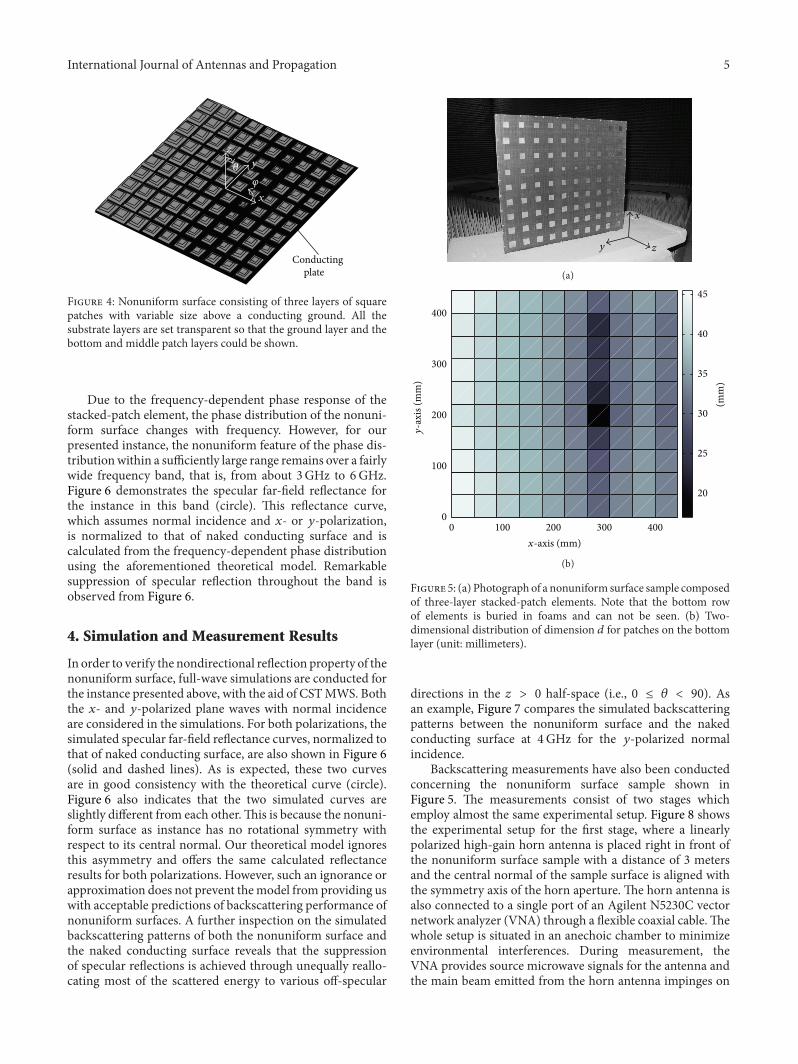

International Journal of
AerospaceEngineeringHindawi Publishing Corporationhttpwwwhindawicom Volume 2014
RoboticsJournal of
Hindawi Publishing Corporationhttpwwwhindawicom Volume 2014
Hindawi Publishing Corporationhttpwwwhindawicom Volume 2014
Active and Passive Electronic Components
Control Scienceand Engineering
Journal of
Hindawi Publishing Corporationhttpwwwhindawicom Volume 2014
International Journal of
RotatingMachinery
Hindawi Publishing Corporationhttpwwwhindawicom Volume 2014
Hindawi Publishing Corporation httpwwwhindawicom
Journal ofEngineeringVolume 2014
Submit your manuscripts athttpwwwhindawicom
VLSI Design
Hindawi Publishing Corporationhttpwwwhindawicom Volume 2014
Hindawi Publishing Corporationhttpwwwhindawicom Volume 2014
Shock and Vibration
Hindawi Publishing Corporationhttpwwwhindawicom Volume 2014
Civil EngineeringAdvances in
Acoustics and VibrationAdvances in
Hindawi Publishing Corporationhttpwwwhindawicom Volume 2014
Hindawi Publishing Corporationhttpwwwhindawicom Volume 2014
Electrical and Computer Engineering
Journal of
Advances inOptoElectronics
Hindawi Publishing Corporation httpwwwhindawicom
Volume 2014
The Scientific World JournalHindawi Publishing Corporation httpwwwhindawicom Volume 2014
SensorsJournal of
Hindawi Publishing Corporationhttpwwwhindawicom Volume 2014
Modelling amp Simulation in EngineeringHindawi Publishing Corporation httpwwwhindawicom Volume 2014
Hindawi Publishing Corporationhttpwwwhindawicom Volume 2014
Chemical EngineeringInternational Journal of Antennas and
Propagation
International Journal of
Hindawi Publishing Corporationhttpwwwhindawicom Volume 2014
Hindawi Publishing Corporationhttpwwwhindawicom Volume 2014
Navigation and Observation
International Journal of
Hindawi Publishing Corporationhttpwwwhindawicom Volume 2014
DistributedSensor Networks
International Journal of