Embed Size (px)
Citation preview

Resist process window characterization for the 45-nm node using an interferometric immersion microstepper
Anatoly Bourov*a,c , Stewart A. Robertsonb, Bruce W. Smithc, Michael A. Slocumc, Emil C. Piscanic a Rochester Institute of Technology, 82 Lomb Memorial Drive, Rochester, NY, USA 14623
b Rohm and Haas Electronic Materials, 455 Forest St, Marlborough, MA, USA 01752 c Amphibian Systems, 125 Tech Park Drive, Rochester, NY, USA 14623
ABSTRACT Projection and interference imaging modalities for application to IC microlithography were compared at the 90 nm imaging node. The basis for comparison included simulated two-dimensional image in resist, simulated resist linesize, as well as experimental resist linesize response through a wide range of dose and focus values. Using resist CD as the main response (both in simulation and experimental comparisons), the two imaging modes were found nearly equivalent, as long as a suitable Focus-Modulation conversion is used. A Focus-Modulation lookup table was generated for the 45 nm imaging node, and experimental resist response was measured using an interferometric tool. A process window was constructed to match a hypothetical projection tool, with an estimated error of prediction of 0.6 nm. A demodulated interferometric imaging technique was determined to be a viable method for experimental measurement of process window data. As long as accurate assumptions can be made about the optical performance of such projection tools, the response of photoresist to the delivered image can be studied experimentally using the demodulated interferometric imaging approach.
Keywords: Interference, immersion, lithography, process window, Bossung, photoresist
1. INTRODUCTION Projection imaging is used extensively in microlithography to create photoresist relief patterns. The pace of progress dictates constant improvement of resolution, both of the imaging tool and the detector, the photoresist. The photoresist development cycle often requires early access to imaging tools well ahead of their widespread availability. This early access can be difficult to obtain, if not sometimes impossible. A simple interferometric imaging technique can yield line/space patterns similar to those of the projection tools, at resolutions not limited by manufacturing constraints but rather by optical properties of the materials.1,2 This approach has been shown to yield results with water as the immersion fluid, and an excimer laser as the radiation source.3 The ability to use this technique for resist characterization has been explored,4 but little comparison has been made directly between the projection imaging and the interferometric imaging. Aerial image-based comparison indicated a possibility of achieving a match between the two approaches,5 but questions remained whether the agreement of two-dimensional images in resist was possible.
The purpose of this work is threefold: to extend the image-based comparison study to two dimensions; secondly, to apply photoresist models to the resulting 2D images; and thirdly, to perform experimental comparison of the resist CD throughout the focus and dose parameter space. When the validity of such approach is established, accurate predictions can be made about photoresist process windows in a projection tool, through photoresist characterization using interferometric imaging experiments.
2. SIMULATION The modeling of images created by projection systems can be readily performed using an available lithography simulator, such as Prolith.6 As interferometric imaging is very similar to a special case of projection imaging, the same modeling tools can be used to simulate image formation in the interferometer as well. Shown in Figure 1 is one of such configurations, along with a depiction of the experimental interferometric exposure system.
* [email protected]; phone 1 585 424-3835; www.amphibianlitho.com

An important aspect of this simulation configuration is the use of an alternating phase shift mask, combined with a coherent on-axis illumination. The source polarization state was chosen to be TE, to match the experimental conditions. A pupil filter was configured to only allow the +1st and -1st diffraction orders to pass through the imaging lens. In this configuration the Fourier spectrum of the illumination impinging onto the image plane is represented by two delta functions, just like that in the interference experiment. This step represents the fully modulated (m=1) step of the interferometric exposure.
In order to understand the effect of the unmodulated (m=0) exposure pass in the interference approach, a 2nd pass was configured in simulation as well. A different pupil filter was used for this pass, only allowing one of the diffraction orders to reach the wafer (see Figure 2). This configuration is a close physical representation of the “flood exposure” step of the demodulated interferometric exposure.
The time ratio between the two exposure steps can be adjusted in simulation, just like it would be in the physical interference exposure process. Any value of the modulation of the final image (between 0 and 1) can be realized using this approach, allowing matching of the contrast in the projection image.
2.1. Two-dimensional image matching and Focus-Modulation lookup table generation The two-dimensional image in resist was calculated using the lithography simulator. The projection case was modeled using a known parameter set that describes the ASML 1150i immersion scanner used in the experimental part. Annular illumination with σi=0.59, and σo=0.89, NA of 0.75, water immersion, and a resist film stack matching the experimental conditions described in Section 3.2 were used. Images in resist were obtained, and average contrast through resist depth was measured for each of the focus values in the test.
The interference case was described using a polarized coherent source combined with a phase shift mask, and the same resist stack. The time ratio between the two exposure passes was adjusted to vary modulation of the image directly. The modulation was set to the average contrast from the projection case, and the images were compared. For all of the focus values considered the average absolute error did not exceed 3.2%. The main source of the error was found to be the standing wave period difference between the projection and the interference images. A summary of the modulation and the average image difference levels is shown in Figure 3(a). The maximum modulation occurred at best focus, and was m=0.56.
Coherent source
Coherent source
pupil
wafer
mask
ArF laser
illuminator
Figure 1: Simulation configuration (left) that allows the use of a projection image simulator to describe image formation in an interferometer system (right). The key features of the simulation are the use of a polarized coherent source, alternating phase shift mask, and a pupil filter to only allow the transmission of the first diffraction order.
pupil
wafer Figure 2: Simulation configuration (left) that describes image formation in the "flood exposure", or zero-modulation step of the interferometric exposure. The actual experimental configuration is shown on the right. The pupil filter is modified in both cases to only allow one of the 1st diffraction orders to reach the wafer.

Analyzing modulation in Projection Image, 90 nm features
defocus (µm)
-0.8 -0.6 -0.4 -0.2 0.0 0.2 0.4 0.6 0.8 1.0
mod
ulat
ion
0.1
0.2
0.3
0.4
0.5
0.6
Image Error
0.00
0.05
0.10
0.15
0.20
modulationImage error
(a)
Analyzing modulation of 45 nm imaging
defocus (µm)
-0.3 -0.2 -0.1 0.0 0.1 0.2 0.3
mod
ulat
ion
0.4
0.5
0.6
0.7
0.8
0.9
Image E
rror
0.00
0.05
0.10
0.15
0.20
modulationImage error
(b)
Figure 3: Focus-Modulation lookup curve for 90 nm (a) and 45 nm (b) features. The average image error remained low throughout the focus range, with the maximum value of 3.2% for both configurations. The modulation at best focus is approximately 0.56 for the 90 nm case.
For the 45 nm simulations, a hypothetical projection tool with the NA of 1.2, TE polarized dipole source with σc=0.90, and σr=0.25 was used. A 6% attenuating phase shift mask with 45 nm lines and a 90 nm pitch was used. The resist stack was configured to match the experimental conditions in Section 3.3, with photoresist thickness of 90 nm. The interferometric simulation configuration used the same resist stack.
The images in resist were once again compared, and the results are presented in Figure 3(b). The main source of image error was found to be the changing image contrast in the projection image. The standing wave period mismatch plays a smaller role, since the resist layer is thinner compared to the 200 nm in the lower NA case. The depth of focus of the higher NA tool is reduced relative to the resist thickness, creating a sharper contrast gradient through the resist thickness. Despite this, the maximum image error was 3.2%.
2.2. Resist profile simulation Full resist process simulations were necessary to understand whether the observed image agreement was going to create a significant linewidth error between the projection and interference cases. Full resist simulations were carried out using JSR AR165J resist model, the default ArF resist model in Prolith v9.2.
2.3. Full process window simulation To compare the resist CD response across a wide range of dose and focus values, a simulation was configured with the layout shown in Figure 4. The Focus-Exposure Matrix data was readily simulated for the projection case, while an additional step was added for the interference imaging. The focus value was converted into the appropriate modulation level using the modulation curves presented in Figure 3. The same resist model was then applied to both cases, and the final CD data was stored for comparison. This approach was applied both to the 90 nm and the 45 nm imaging configurations.

F,E range
Resist Model
Projection Image Formation Interference Image
Projection Bossung
-0.8 -0.6 -0.4 -0.2 0.0 0.2 0.4 0.6 0.820
40
60
80
100
120
140
160
A n a ly zin g m o du la t io n in P ro jec t io n Im a g e
foc u s (µm )
-0 .8 -0 .6 - 0.4 - 0.2 0 .0 0 .2 0 .4 0 .6 0 .8 1 .0
mo
du
latio
n
0 .1
0 .2
0 .3
0 .4
0 .5
0 .6
Ima
ge
Err
or
0 .0 2
0 .0 4
0 .0 6
0 .0 8
0 .1 0
m od u la ti onIm ag e e rro r
F-M conversion
Interference Bossung
-0.8 -0.6 -0.4 -0.2 0.0 0.2 0.4 0.6 0.8
CD (nm)
20
40
60
80
100
120
140
160
Resist CD
Compare
CD CD
Figure 4: Outline of simulation-based comparison. The defocus value was converted to the modulation value using a pre-determined FM lookup table. Both image formation approaches were used to model the image, followed by resist modeling using the same resist model. The resist CD as a function of dose and defocus was then used as a comparison metric.
The stored data was plotted on the same graph, and is presented in Figure 5. After a 0.05 µm focus shift was applied in the 90 nm case, the average error was measured at 0.5 nm across all the data points collected. No focus shift was necessary in the 45 nm case, and the same amount of error was observed.
Projection vs. Interferometry, Simulation Resist CD, 90 nm feature
defocus (µm)
-0.8 -0.6 -0.4 -0.2 0.0 0.2 0.4 0.6 0.8
CD
(nm
)
20
40
60
80
100
120
140
160
(a)
Projection vs. Interferometry, Simulation Resist CD, 45 nm features
defocus (µm)
-0.3 -0.2 -0.1 0.0 0.1 0.2 0.3
CD
(nm
)
20
40
60
80
InterferenceProjection
(b)
Figure 5: Comparison of simulated resist CD response to the projection (dots) and interference (lines) image formation systems. The 90 nm half-pitch imaging (a) is compared on the left, while the 45 nm imaging (b) is shown on the right. The average error was 0.5 nm across the whole defocus-dose space in both cases.
Projection Interference

3. EXPERIMENTAL
3.1. Data analysis models A simple model was developed to analyze the experimental CD data, with respect to variation in image modulation and delivered dose. Using a sinusoidal latent image form assumption,4 and a threshold model for the resist, the linesize was calculated as a direct function of the two parameters, as seen in Equation (1).
1arccos 1 s
R
EpCDm Eπ
⎛ ⎞⎛ ⎞= −⎜ ⎟⎜ ⎟⎝ ⎠⎝ ⎠
(1)
Here mR is the modulation of the latent image in the resist, E is the exposure dose, and Es is the dose-to-size, and p is the pitch of the image. In order to facilitate generalization, the function was expanded into a Taylor series, assuming small deviation of E from Es, see Equation (2).
3 5
3
1 11 1 12 6
s s s
R R
E E Ep p pCD Om E E Emπ π
⎛ ⎞ ⎛ ⎞ ⎛ ⎞= + − + − + −⎜ ⎟ ⎜ ⎟ ⎜ ⎟⎝ ⎠ ⎝ ⎠ ⎝ ⎠
(2)
To prepare for regression analysis of the experimental data, the model terms were expanded, and the latent image modulation was replaced by optical image modulation m. The addition of a random term, ε, is necessary to account for experimental error, as well as any loss of accuracy due to the nature of the Taylor expansion. The higher order terms could be included if lack-of-fit tests should indicate the necessity, but their general form should remain the same, 1/mk and 1/El.
1 1 1CD a b c dm E m E
ε= + + + +⋅
(3)
The analysis process of the experimental data was greatly facilitated by the simplified model of Equation (3). The data collection process was determined to be more resistant to experimental noise when the interferometer data was evenly spaced with respect to modulation instead of focus. With the data collection grid based on modulation instead of equivalent focus, more points were collected at the lower levels of modulation, and the quality of fitted models was better. A better quality of fit could be obtained using fewer model terms, and therefore the interferometric exposure grid was based on modulation. For comparison purposes, the experimental CD(m,E) function was remapped into the CD(F,E) using a calculated Focus-Modulation curve m(F). The outline of the whole comparison process is given in Figure 6.
An additional benefit of this approach is separation of experimental resist performance measurements from the imaging tool prediction modeling. Different Focus-Modulation curves can be applied to the same set of experimental data to analyze process windows with any projection tool settings, as long as the pitch of the image is kept at a constant.
3.2. 90 nm imaging comparison To validate the simulation-based comparisons between the two imaging modes, an experimental study was performed. Using the same resist process two sets of resist CD measurements were collected, one from a projection imaging tool, another from an interference tool, both configured for 90 nm nominal line width (half-pitch). Rohm and Haas XP 4946 photoresist was used with a thickness of 200 nm after the 60 s/90 °C soft-bake. The resist was coated on top of the AR40 BARC material, which was 80 nm thick. The baking conditions for the BARC material were 60 seconds at 215 °C. Following the exposures the wafers were baked for 60 seconds at 95 °C, and then developed for 60 seconds in a 0.26 normality TMAH solution.
The projection imaging was realized using an ASML 1150i immersion scanner with conditions matching those used for the simulation. The NA of 0.75 and an annular configuration with σi=0.59, and σo=0.89 was used. An attenuating phase shift mask with a 6% transmission level, and a dense-line pattern of 180 nm pitch was used as the imaging object. This tool accepted 300 mm substrates, and all sample preparation and processing was done using the track attached to the scanner.

Experimental Process Window, 90 nm
modulation0.2 0.4 0.6 0.8 1.0
CD
(nm
)
40
50
60
70
80
90
100
110
120
rawsmoothed
Experimental CD, steps of equal dose
focus (µm)-0.6 -0.4 -0.2 0.0 0.2 0.4 0.6 0.8
CD
(nm
)
40
60
80
100
120
140Experimental CD, steps of equal dose
focus (µm)-0.6 -0.4 -0.2 0.0 0.2 0.4 0.6 0.8
CD
(nm
)
40
60
80
100
120
140
Analyzing modulation in Projection Image
focus (µm)
-0.8 -0.6 -0.4 -0.2 0.0 0.2 0.4 0.6 0.8 1.0
mod
ulat
ion
0.1
0.2
0.3
0.4
0.5
0.6
modulation
Figure 6: Outline of data flow for the experimental comparison of the projection and interference systems. The projection data was collected directly, while the interference data was analyzed using a modulation-dose fitting model. The Focus-Modulation conversion was then applied to allow representation of the ME data in FE space. The projection and interference datasets were then directly compared.
The interference imaging was realized with an Amphibian XIS-SW7 immersion/dry ministepper, configured with the NA=0.54 imaging prism, designed to create patterns of 180 nm pitch on the wafer. This tool was able to process 200 mm wafers in either Modulation-Exposure array or Focus-Exposure array mode. The Focus-Modulation conversion table (Figure 3(a)) was imported into the exposure control software and used for the FE array. The immersion configuration was used to match the projection system, with a fluid gap of 0.3 mm. No attempt was made to calibrate the dose level based on the imaging performance, and the dose expansion factor of 200 cm2 was used. The photoresist coating and development was performed using an automated track, while the PEB was done using a Brewer Science CEE 1000 hotplate in proximity baking mode. The resist image inspection was carried out using a top-down Hitachi S-9300 SEM, both for 200 mm and 300 mm substrates.
3.3. Measuring resist response in 45 nm imaging mode Only the interferometric mode resist response was collected, using a different Amphibian XIS-SW ministepper. The photoresist used in this study was JSR 1941J, with a thickness of 90 nm. The softbake and the post-exposure bake conditions were 60 seconds at 110 °C. The dose calibration was performed using this photoresist, and the dose expansion factor was set to 28 cm2, so that the dose-to-size value was approximately 20 mJ/cm2. The Brewer Science ARC 29A at 41 nm thickness, processed for 90 seconds at 200 °C served as the reflection suppression layer. The JSR TCX-014 material with a thickness of 30 nm was used as a top barrier. The interference prism with the NA=1.05 and a water gap thickness of 0.3 mm provided the main imaging configuration for the microstepper.
The processed wafer inspection was once again done using a Hitachi S-9300 SEM. It should be noted that 45 nm features are beyond the intended resolution limit of this instrument, which likely introduced larger relative amount of noise into the experimental data when compared to that for the 90 nm study.
Projection Interference

4. EXPERIMENTAL MATCHING OF PROJECTION AND INTERFEROMETRY
4.1. Comparing FEM for 90 nm node from projection and interferometric tools The exposed FEM wafers were inspected; a summary of captured images for the 90 nm case using interferometric imaging is shown in Figure 7. Behavior typical of a process-window exposure set was observed, with reduced range of dose at higher defocus values. The highlighted portions of Figure 7 were then used for Depth-of-Focus and Exposure Latitude analysis. In order to perform a direct comparison of failure points for Depth-of-Focus analysis, the two series produced by the projection tool and the interferometric tool are shown next to each other in Figure 8. The dose levels were chosen to produce a similar CD value, and the defocus value was converted using the F-M lookup table.
Figure 7: Process window SEM images for the 90 nm resist lines formed using the interference tool. The defocus values correspond to the projection tool, and were converted to modulation automatically during the exposure. Highlighted are the SEM images that were used for consequent DOF and EL analysis.

Figure 8: Direct comparison of SEM images of lines formed with projection and interference imaging for the 90 nm node. Defocus was varied directly for the projection system, and via an F-M conversion table for the interference case.
For the exposure latitude comparison the CD data at best focus, and a matched modulation level was used. A simple fit to the data was made using the following function, similar to the Equation (3), but without the varying modulation component
1CD a bE
ε= + + (4)
Here, ε is a random variable, describing experimental error. The R2adj was 0.99 for the projection case, and 0.89 for the
interference case. Using a CD latitude value of ±10 %, and the target CD value of 90 nm, the relative exposure latitude was calculated to be 11.7 ± 0.2 % for the projection case, and 11.7 ± 1.1 % for the interference case. The uncertainty in the values was estimated using statistical analysis of the fit quality.
Calculating exposure latitude for ASML 1150i, best focus
Dose (mJ/cm2)
14 16 18 20 22
CD
(nm
)
50
60
70
80
90
100
110
120
EL=11.7%
(a)
Calculating exposure latitude for Amphibian XIS, m=0.56
Dose (mJ/cm2)
1.0 1.1 1.2 1.3 1.4 1.5
CD
(nm
)
50
60
70
80
90
100
110
120
EL=11.7%
(b)
Figure 9: Exposure latitude data for projection imaging (a) and interference imaging (b). Both systems were configured for 90 nm half-pitch imaging. No attempt was made to calibrate the dose on the interferometric tool. The relative exposure latitude values agree well.
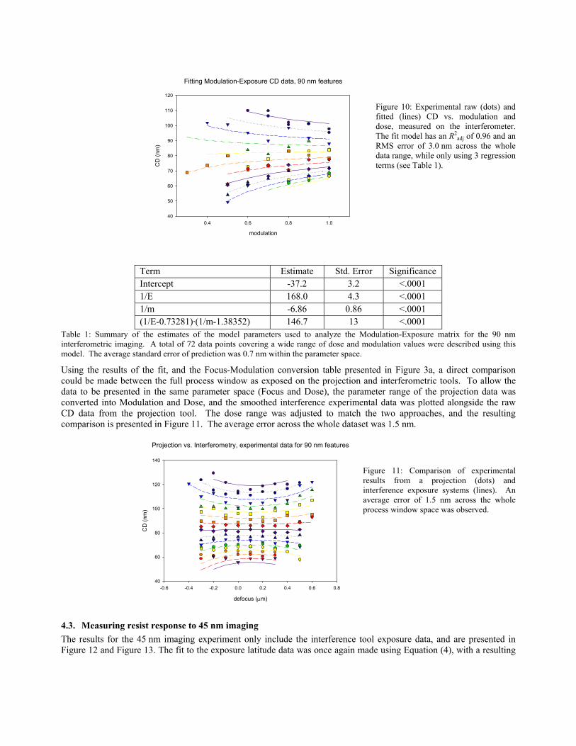
4.2. 90 nm process window comparisons For a quantitative comparison of the full process window, the data from the Modulation Exposure Matrix was used. This set of images was also inspected in the SEM, and the measured linewidth values are plotted in Figure 10. Shown in the same image is the fit to this data, using a simple regression model presented in Equation (3). The fit was performed in a least-squared sense, using an Analysis of Variance approach. The R2
adj was 0.96 and the root mean square error was estimated at 3.0 nm, while the average error of prediction was 0.7 nm. The resulting values of the coefficients along with their respective error values are shown in Table 1.
Fitting Modulation-Exposure CD data, 90 nm features
modulation
0.4 0.6 0.8 1.0
CD
(nm
)
40
50
60
70
80
90
100
110
120
Figure 10: Experimental raw (dots) and fitted (lines) CD vs. modulation and dose, measured on the interferometer. The fit model has an R2
adj of 0.96 and an RMS error of 3.0 nm across the whole data range, while only using 3 regression terms (see Table 1).
Term Estimate Std. Error Significance Intercept -37.2 3.2 <.0001 1/E 168.0 4.3 <.0001 1/m -6.86 0.86 <.0001 (1/E-0.73281)·(1/m-1.38352) 146.7 13 <.0001
Table 1: Summary of the estimates of the model parameters used to analyze the Modulation-Exposure matrix for the 90 nm interferometric imaging. A total of 72 data points covering a wide range of dose and modulation values were described using this model. The average standard error of prediction was 0.7 nm within the parameter space.
Using the results of the fit, and the Focus-Modulation conversion table presented in Figure 3a, a direct comparison could be made between the full process window as exposed on the projection and interferometric tools. To allow the data to be presented in the same parameter space (Focus and Dose), the parameter range of the projection data was converted into Modulation and Dose, and the smoothed interference experimental data was plotted alongside the raw CD data from the projection tool. The dose range was adjusted to match the two approaches, and the resulting comparison is presented in Figure 11. The average error across the whole dataset was 1.5 nm.
Projection vs. Interferometry, experimental data for 90 nm features
defocus (µm)
-0.6 -0.4 -0.2 0.0 0.2 0.4 0.6 0.8
CD
(nm
)
40
60
80
100
120
140
Figure 11: Comparison of experimental results from a projection (dots) and interference exposure systems (lines). An average error of 1.5 nm across the whole process window space was observed.
4.3. Measuring resist response to 45 nm imaging The results for the 45 nm imaging experiment only include the interference tool exposure data, and are presented in Figure 12 and Figure 13. The fit to the exposure latitude data was once again made using Equation (4), with a resulting

R2adj of 0.82. The calculated value of relative exposure latitude, using the CD latitude value of ±10 %, and the target
CD value of 45 nm was EL = 19.0 ± 2.9 %. The value is higher than that reported for the 90 nm case, largely due to the fact that the best focus modulation value was 0.98 for this case, vs. 0.56 for the 90 nm experiment.
CD vs. Dose at best focus, 45 nm features
Dose (mJ/cm2)
18 19 20 21 22 23
CD
(nm
)
34
36
38
40
42
44
46
48
Figure 12: Exposure latitude for 45 nm process, at matched best focus, measured using the interferometric imaging system.
The analysis of the full Modulation-Exposure matrix was once again carried out using the CD model shown in Equation (3). The experimental data and the lines representing the fit model are shown in Figure 13. The values of the model terms and their error estimates are presented in Table 2. The quality of the fit was represented by an R2
adj of 0.82, and a root mean square error of 1.9 nm. The average error of predicted values was 0.6 nm.
CD vs. modulation, fitting the data for 45 nm features
modulation
0.4 0.5 0.6 0.7 0.8 0.9 1.0
CD
(nm
)
34
36
38
40
42
44
46
48
50
52
Exp 17.85 Exp 18.38 Exp 18.91 Exp 19.44 Exp 19.97 Exp 20.5 Exp 21.03 Exp 21.56 Exp 22.09 Exp 22.62
Figure 13: Experimental raw (dots) and fitted (lines) CD vs. modulation and dose. The fit model has R2
adj of 0.82 and an RMS error of 1.9 nm across whole range, while using only 3 regression terms.
Term Estimate Std. Error Significance Intercept -24.6 6.3 0.0005 1/E 1370 154 <.0001 1/m -2.7 2.1 0.21 (1/m-1.24157)·(1/E-0.05064) 2161 747 0.0073
Table 2: Summary of the estimates of the fit parameters used to analyze the Modulation-Exposure matrix for the 45 nm interferometric imaging. A total of 32 data points covering a wide range of dose and modulation values were described using this model.
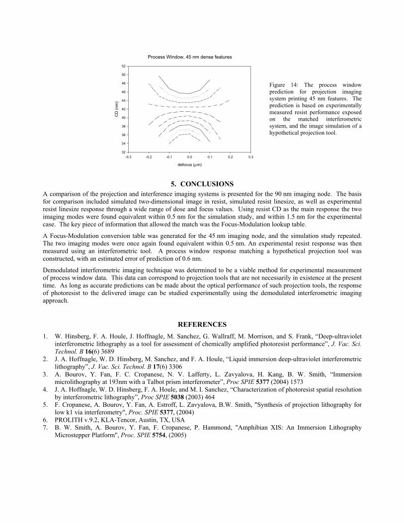
4.4. Process window synthesis based on experimental resist response The fitted resist performance data was combined with the Focus-Modulation curve to map the resist CD in the Focus-Dose parameter space. The resulting process window plot is presented in Figure 14. Assuming no errors in the Focus-Modulation conversion table, the error of prediction is comparable to that of the CD(m,E) function, which was 0.6 nm.
Process Window, 45 nm dense features
defocus (µm)
-0.3 -0.2 -0.1 0.0 0.1 0.2 0.3
CD
(nm
)
32
34
36
38
40
42
44
46
48
50
52
Figure 14: The process window prediction for projection imaging system printing 45 nm features. The prediction is based on experimentally measured resist performance exposed on the matched interferometric system, and the image simulation of a hypothetical projection tool.
5. CONCLUSIONS A comparison of the projection and interference imaging systems is presented for the 90 nm imaging node. The basis for comparison included simulated two-dimensional image in resist, simulated resist linesize, as well as experimental resist linesize response through a wide range of dose and focus values. Using resist CD as the main response the two imaging modes were found equivalent within 0.5 nm for the simulation study, and within 1.5 nm for the experimental case. The key piece of information that allowed the match was the Focus-Modulation lookup table.
A Focus-Modulation conversion table was generated for the 45 nm imaging node, and the simulation study repeated. The two imaging modes were once again found equivalent within 0.5 nm. An experimental resist response was then measured using an interferometric tool. A process window response matching a hypothetical projection tool was constructed, with an estimated error of prediction of 0.6 nm.
Demodulated interferometric imaging technique was determined to be a viable method for experimental measurement of process window data. This data can correspond to projection tools that are not necessarily in existence at the present time. As long as accurate predictions can be made about the optical performance of such projection tools, the response of photoresist to the delivered image can be studied experimentally using the demodulated interferometric imaging approach.
REFERENCES 1. W. Hinsberg, F. A. Houle, J. Hoffnagle, M. Sanchez, G. Wallraff, M. Morrison, and S. Frank, “Deep-ultraviolet
interferometric lithography as a tool for assessment of chemically amplified photoresist performance”, J. Vac. Sci. Technol. B 16(6) 3689
2. J. A. Hoffnagle, W. D. Hinsberg, M. Sanchez, and F. A. Houle, “Liquid immersion deep-ultraviolet interferometric lithography”, J. Vac. Sci. Technol. B 17(6) 3306
3. A. Bourov, Y. Fan, F. C. Cropanese, N. V. Lafferty, L. Zavyalova, H. Kang, B. W. Smith, “Immersion microlithography at 193nm with a Talbot prism interferometer”, Proc SPIE 5377 (2004) 1573
4. J. A. Hoffnagle, W. D. Hinsberg, F. A. Houle, and M. I. Sanchez, “Characterization of photoresist spatial resolution by interferometric lithography”, Proc SPIE 5038 (2003) 464
5. F. Cropanese, A. Bourov, Y. Fan, A. Estroff, L. Zavyalova, B.W. Smith, "Synthesis of projection lithography for low k1 via interferometry", Proc. SPIE 5377, (2004)
6. PROLITH v.9.2, KLA-Tencor, Austin, TX, USA 7. B. W. Smith, A. Bourov, Y. Fan, F. Cropanese, P. Hammond, "Amphibian XIS: An Immersion Lithography
Microstepper Platform", Proc. SPIE 5754, (2005)